measurements 1: receiving techniques
TRANSCRIPT

Measurements 1: Signal Measurements 1: Signal receiving techniquesreceiving techniques
Fritz Caspers
CAS, Aarhus, June 2010

Contents• The radio frequency (RF) diode• Superheterodyne concept• Spectrum analyzer• Oscilloscope• Vector spectrum and FFT analyzer• Decibel• Noise basics• Noise‐figure measurement with the spectrum
analyzer
CAS, Aarhus, June 2010 2

The RF diode (1)• We are not discussing the generation of RF signals here, just the detection
• Basic tool: fast RF* diode
(= Schottky diode)
• In general, Schottky diodes are fast
but still have a voltage dependent
junction capacity (metal – semi‐
conductor junction)
• Equivalent circuit:
3CAS, Aarhus, June 2010
*Please note, that in this lecture we will use RF for both the RF and micro wave (MW) range, since
the borderline between RF and MW is not defined unambiguously
Video
output
A typical RF detector diodeTry to guess from the type of the
connector which side is the RF input
and which is the output

The RF diode (2)
• Characteristics of a diode:• The current as a function of the voltage for a barrier diode can
be
described by the Richardson equation:
4CAS, Aarhus, June 2010
The RF diode is NOT an ideal
commutator for small
signals! We cannot apply big
signals otherwise burnout

• In a highly simplified manner, one can approximate this expression as:
• and show as sketched in the following, that the RF rectification
is linked to
the second derivation (curvature) of the diode characteristics:
CAS, Aarhus, June 2010 5
The RF diode (3)
VJ
…
junction voltage

The RF diode (4)• This diagram depicts the so called square‐law region where the output
voltage (VVideo
) is proportional to the input power
• The transition between the linear region and the square‐law region is
typically between ‐10 and ‐20 dBm RF power (see diagram)6CAS, Aarhus, June 2010
• Since the input power
is proportional to the
square of the input
voltage (VRF2) and the
output signal is
proportional to the
input power, this
region is called square‐
law region.
• In other words:
VVideo
~ VRF2
‐20 dBm = 0.01 mW
Linear Region

• Due to the square‐law characteristic we arrive at the thermal noise region
already for moderate power levels (‐50 to ‐60 dBm) and hence the VVideo
disappears in the thermal noise
• This is described by the term
tangential signal sensitivity (TSS)
where the detected signal
(Observation BW, usually 10 MHz)
is 4 dB over the thermal noise floor
CAS, Aarhus, June 2010 7
The RF diode (5)
Time
Voltage
Output
4dB

The RF mixer (1)• For the detection of very small RF signals we prefer a device that has a linear
response over the full range (from 0 dBm ( = 1mW) down to thermal noise = ‐174 dBm/Hz = 4∙10‐21
W/Hz) • This is the RF mixer which is using 1, 2 or 4 diodes in different configurations
(see next slide)
• Together with a so called LO (local oscillator) signal, the mixer works as a
signal multiplier with a very high dynamic range since the output signal is
always in the “linear range”
provided, that the mixer is not in saturation with
respect to the RF input signal (For the LO signal the mixer should always be in
saturation!)
• The RF mixer is essentially a multiplier implementing the function
f1
(t) ∙
f2
(t) with f1
(t) = RF signal and f2
(t) = LO signal
• Thus we obtain a response at the IF (intermediate frequency) port that is at
the sum and difference frequency of the LO and RF signals
CAS, Aarhus, June 2010 8
)])cos(())[cos((21)2cos()2cos( 2121212211 tfftffaatfatfa

The RF mixer (2)• Examples of different mixer configurations
CAS, Aarhus, June 2010 9
A typical coaxial mixer (SMA connector)
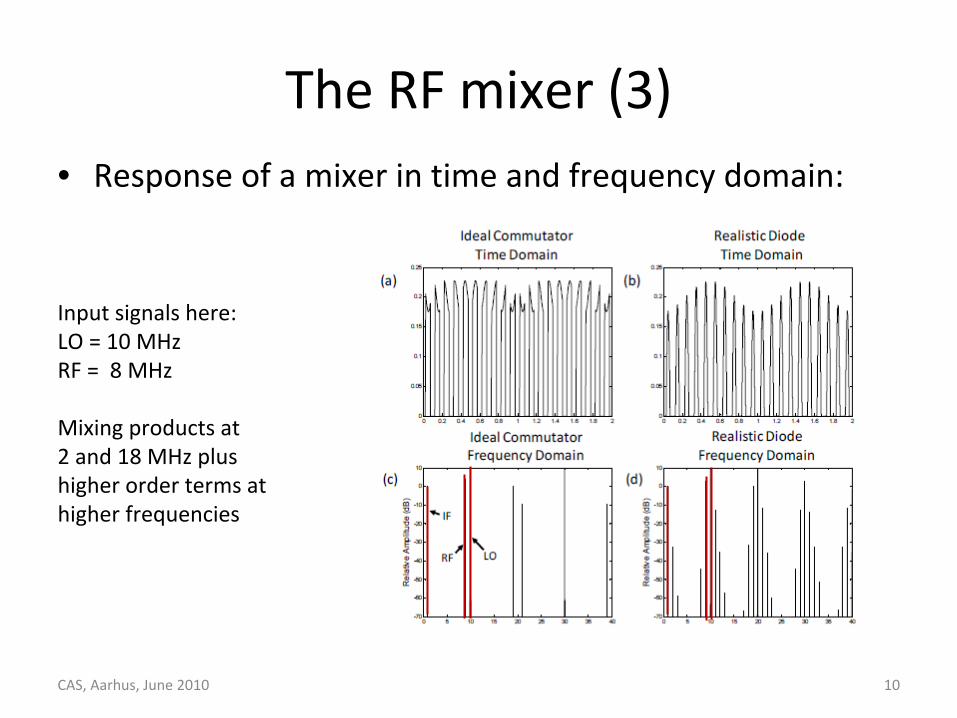
The RF mixer (3)• Response of a mixer in time and frequency domain:
CAS, Aarhus, June 2010 10
Input signals here:LO = 10 MHzRF = 8 MHz
Mixing products at2 and 18 MHz plushigher order terms at
higher frequencies

The RF mixer (4)
• Dynamic range and IP3 of an RF mixer• The abbreviation IP3 stands for
the third order intermodulationpoint where the two lines shown in the right diagram intersect. Two signals (f1
,f2
> f1
) which areclosely spaced by Δf in frequency are simultaneously applied to the DUT.The intermodulation products appear at+
Δf above f2
and at –
Δf below f1
.• This intersection point is usually
not measured directly, but extrapolated from measurementdata at much smaller power levelsin order to avoid overload anddamage of the DUTCAS, Aarhus, June 2010 11

Solid state diodes used for RF applications• There are many other diodes which are used for different applications in
the RF domain
• Varactor diodes: for tuning application
• PIN diodes: for electronically variable RF attenuators
• Step Recovery diodes: for frequency multiplication and pulse sharpening
• Mixer diodes, detector diodes: usually Schottky diodes
• TED (GUNN, IMPATT, TRAPATT etc.): for oscillator
• Parametric amplifier Diodes: usually variable capacitors (vari caps)
• Tunnel diodes: rarely used these days, they have negative impedance and
are usually used for very fast switching and certain low noise amplifiersCAS, Aarhus, June 2010 12

Measurement devices (1)
• There are many ways to observe RF signals. Here we give a brief
overview of the four main tools we have at hand
• Oscilloscope: to observe signals in time domain– periodic signals
– burst signal
– application: direct observation of signal from a pick‐up, shape of common
230 V mains supply voltage, etc.
• Spectrum analyser: to observe signals in frequency domain– sweeps through a given frequency range point by point
– application: observation of spectrum from the beam or of the spectrum
emitted from an antenna, etc.
13CAS, Aarhus, June 2010

Measurement devices (2)
• Dynamic signal analyser (FFT analyser)– Acquires signal in time domain by fast sampling– Further numerical treatment in digital signal processors (DSPs)– Spectrum calculated using Fast Fourier Transform (FFT)– Combines features of a scope and a spectrum analyser: signals can be looked at
directly in time domain or in frequency domain
– Contrary to the SPA, also the spectrum of non‐repetitive signals and transients
can be observed
– Application: Observation of tune sidebands, transient behaviour of a phase
locked loop, etc.
• Network analyser– Excites a network (circuit, antenna, amplifier or such) at a given CW frequency
and measures response in magnitude and phase => determines S‐parameters
– Covers a frequency range by measuring step‐by‐step at subsequent frequency
points
– Application: characterization of passive and active components, time domain
reflectometry by Fourier transforming reflection response, etc.
14CAS, Aarhus, June 2010

Superheterodyne Concept (1)Design and its evolutionThe diagram below shows the basic elements of a single conversion superheterodyne (“superhet”
or just “super”) receiver. The essential elements of a local oscillator and a mixer followed by a
fixed‐tuned filter and IF amplifier are common to all superhet circuits. [super a
mixture of latin and greek … it means: another force becomes superimposed.
The advantage to this method is that most of the radio's signal path has to be sensitive to only a
narrow range of frequencies. Only the front end (the part before
the frequency converter stage)
needs to be sensitive to a wide frequency range. For example, the front end might need to be
sensitive to 1–30
MHz, while the rest of the radio might need to be sensitive only
to 455
kHz, a
typical IF.
en.wikipedia.org
This type of configuration we find in any
conventional (= not digital) AM or FM
radio receiver.
15CAS, Aarhus, June 2010

Superheterodyne Concept (2)
en.wikipedia.org
RF
Amplifier = wideband frontend amplification (RF = radio frequency)The Mixer can be seen as an analog multiplier which multiplies the RF signal with the LO
(local
oscillator) signal. The local oscillator has its name because it’s an oscillator situated in the receiver locally and not
far away as the radio transmitter to be received.IF
stands for intermediate frequency. The demodulator can be an amplitude modulation (AM) demodulator (envelope detector) or a
frequency modulation (FM) demodulator, implemented e.g. as a PLL
(phase locked loop).The tuning of a normal radio receiver is done by changing the frequency of the LO, not of the IF
filter.Note that also multiple (double, triple, quadruple ) superhet stage concept exist and are used
for very high quality receivers.
IF
16CAS, Aarhus, June 2010
Spectrum Analyzer (1)
• Radio‐frequency spectrum‐analysers (SPA or SA) can be found in virtually
every control‐room of a modern particle accelerator.
• They are used for many aspects of beam diagnostics including Schottky
signal acquisition and RF observation. We discuss first the application of
classical super‐heterodyne SPAs and later systems based on the
acquisition of time domain traces and subsequent Fourier transform (FFT
analysers).
• Such a super‐heterodyne SPA is very similar (in principle) to any AM or FM
radio receiver. The incoming RF‐signal is moderately amplified
(sometimes with adjustable gain) and then sent to the RF‐port of a mixer.
17CAS, Aarhus, June 2010

Example for Application of the Superheterodyne Concept in a Spectrum Analyzer
Agilent, ‘Spectrum Analyzer Basics,’
Application Note 150, page 10 f.
The center frequency is fixed, but
the bandwidth of theIF filter can be modified.
The video filter is a simple low‐pass
with variable bandwidth before the
signal arrives to the vertical
deflection plates of the cathode ray
tube.
18CAS, Aarhus, June 2010

Spectrum Analyzer (2)• The most important knobs on a spectrum
analyzer are:1.
Vertical parameters:
1.
Reference Level
2.
Sensitivity
3.
Display format (Lin‐log)
4.
Video bandwidth (low pass for vertical deflection)
5.
Vertical scale (1, 5, 10 dB per division)
2.
Horizontal parameters1.
Sweep time
2.
Frequency span
3.
Resolution bandwidth
4.
Number of points
CAS, Aarhus, June 2010 19
Caution: These Parameters should not be adjusted independent from each otherThe setting time of the resolution BW filter must be kept in mind.

Spectrum Analyzer (3)• Impact of the variable resolution BW (upper half) and video BW (lower
half respectively):
CAS, Aarhus, June 2010 20

Spectrum Analyzer (4)
CAS, Aarhus, June 2010 21

Oscilloscope (1)• The architecture of an oscilloscope has changed considerably over the last
decades
CAS, Aarhus, June 2010

Oscilloscope (2)• One of the many interesting feature
of modern oscilloscopes is that they
can change the sampling rate
through the sweep in a programmed
manner.
• This can be very helpful for detailed
analysis in certain time windows
• Typical sampling rates are between
a factor 2.5 and 4 of the maximum
frequency (Nyquist requires a real
time minimum sampling rate as
twice fmax
)
CAS, Aarhus, June 2010

Oscilloscope (3)
• Sequential sampling requires a
pre trigger (required to open
the sampling gate) and permits
a non real time bandwidth of
more than 50GHz with modern
scopes
• Random sampling (rarely used
these days) was developed
about 40 years ago for the
case that no pre trigger was
availiable and relying on a
strictly periodic signal to
predict a pre trigger from the
measured periodicity
CAS, Aarhus, June 2010
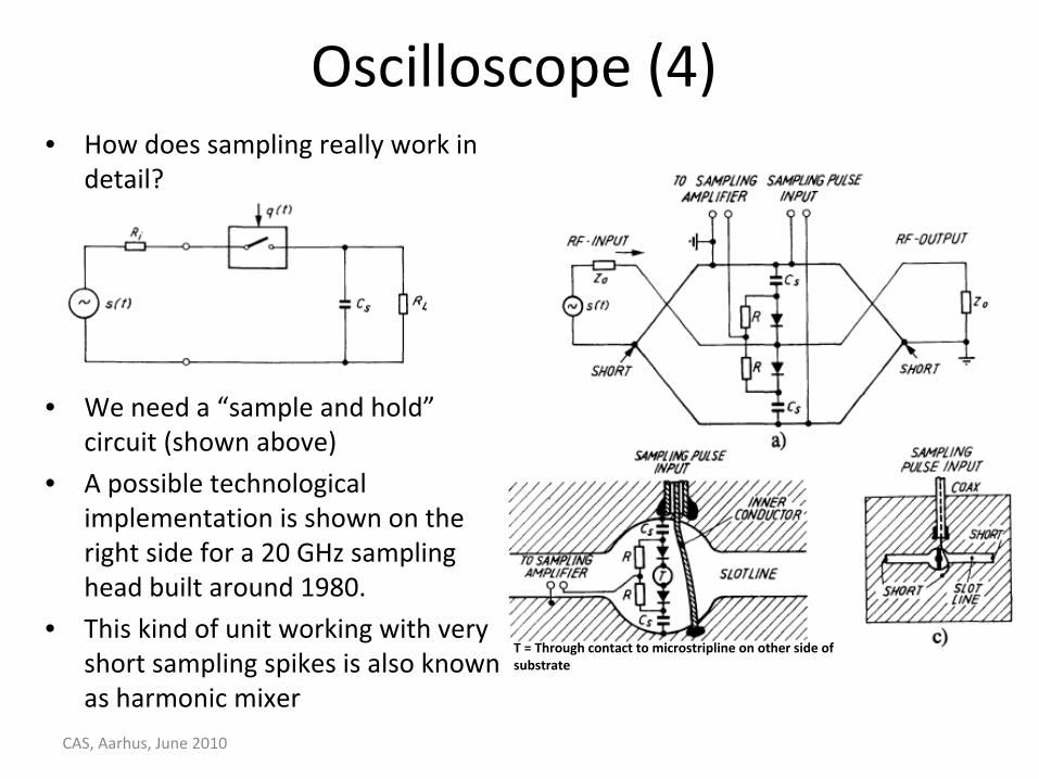
Oscilloscope (4)• How does sampling really work in
detail?
• We need a “sample and hold”
circuit (shown above)
• A possible technological
implementation is shown on the
right side for a 20 GHz sampling
head built around 1980.
• This kind of unit working with very
short sampling spikes is also known
as harmonic mixer
CAS, Aarhus, June 2010
T = Through contact to microstripline on other side of
substrate

Vector spectrum analyzer• The modern vector spectrum analyzer (VSA) is essentially a combination
of a two channel digital oscilloscope and a spectrum analyzer FFT display
• The incoming signal gets down mixed, bandpass (BP) filtered and passes
an ADC (generalized Nyquist for BP signals; fsample
≥
2BW).• The digitized time trace then is split into an I (in phase) and Q
(quadrature, 90 degree offset) component with respect to the phase of
some reference oscillator. Without this reference, the term vector is
meaningless for a spectral component
CAS, Aarhus, June 2010 Note that a VSA can easily separate AM and FM components

Vector spectrum analyzer• Example of vector spectrum analyzer display and performance:
CAS, Aarhus, June 2010
Single shot FFT display similar to a very
slow scan on a swept spectrum
analyzer
Spectrogram display containing about 200
traces as shown on the left side in color
coding. Time runs from top to bottom
Electron cloud measurements in the CERN SPS taken 2008
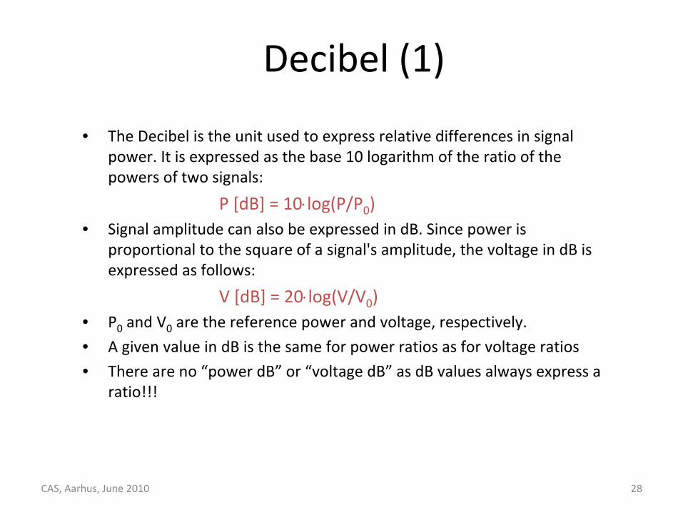
Decibel (1)
• The Decibel is the unit used to express relative differences in signal
power. It is expressed as the base 10 logarithm of the ratio of the
powers of two signals:
P [dB] = 10log(P/P0
)• Signal amplitude can also be expressed in dB. Since power is
proportional to the square of a signal's amplitude, the voltage in dB is
expressed as follows:
V [dB] = 20log(V/V0
)• P0
and V0
are the reference power and voltage, respectively.
• A given value in dB is the same for power ratios as for voltage ratios
• There are no “power dB”
or “voltage dB”
as dB values always express a
ratio!!!
28CAS, Aarhus, June 2010

Decibel (2)• Conversely, the absolute power and voltage can be obtained from dB
values by
• Logarithms are useful as the unit of measurement because (1) signal
power tends to span several orders of magnitude and (2) signal
attenuation losses and gains can be expressed in terms of subtraction and
addition.
20[dB]
010[dB]
0 10 ,10VP
VVPP
29CAS, Aarhus, June 2010

Decibel (3)• The following table helps to indicate the order of magnitude associated
with dB:
• Power ratio = voltage ratio squared!
• S parameters are defined as ratios and sometimes expressed in dB, no
explicit reference needed!
power ratio V, I, E or H ratio, Sij
-20 dB 0.01 0.1-10 dB 0.1 0.32-3 dB 0.50 0.71-1 dB 0.74 0.890 dB 1 1
1 dB 1.26 1.123 dB 2.00 1.4110 dB 10 3.1620 dB 100 10n * 10 dB 10n 10n/2
30CAS, Aarhus, June 2010

Decibel (4)
• Frequently dB values are expressed using a special reference
level and not SI units. Strictly speaking, the reference value
should be included in parenthesis when giving a dB value, e.g.
+3 dB (1W) indicates 3 dB at P0
= 1 Watt, thus 2 W.
• For instance, dBm
defines dB using a reference level of P0
= 1
mW. Often a reference impedance of 50 is assumed. • Thus, 0 dBm correspond to ‐30 dBW, where dBW
indicates a
reference level of P0
=1W.
• Other common units: – dBmV for the small voltages, V0
= 1 mV
– dBV/m for the electric field strength radiated from an antenna, E0
= 1
V/m
31CAS, Aarhus, June 2010

Definition of the Noise Figure
dBNSNSNF
oo
iilg10
BGkTNBGkT
BGkTN
GNN
NSNSF Ro
i
o
oo
ii
0
0
0
• F
is the Noise factor
of the receiver
• Si
is the available signal power at input
• Ni
=kT0
B
is the available noise power at input
• T0
is the absolute temperature of the source resistance
• No
is the available noise power at the output , including
amplified input noise
• G
is the available receiver gain
• B
is the effective noise bandwidth of the receiver
• If the noise factor is specified in a logarithmic unit, we use the
term Noise Figure
(NF).
Very good link: http://www.ieee.li/pdf/viewgraphs_mohr_noise.pdf

Shot noise in a vacuum diode (1)
Consider a vacuum diode where single electrons are passing through in a
statistical manner (left figure) with the travel time
Due to the dD/dt (D = E) we get a current linearly increasing vs time when
the electron approaches the flat anode.
We assume a diode in a saturated regime (space charge neglected) and
obtain after some math for frequencies with a period >>
for the spectral
density S
i
() of the short circuit current the Schottky equation:
with e= 1.6e‐19
As and the mean current I0
=e vmean
eISi 02)(
e-
C
A
d z
i(t)
=U0
+-
e-
C
A
d z
i(t)
=U0
e-
C
A
d z
i(t)
=U0
+-
t
i(t)
33CAS, Aarhus, June 2010

Shot noise in vacuum diodes (2)
obviously the travel time
plays a very important role for the frequency limit
The value for
in typical vacuum diodes operated at a few 100 Volts is around a
fraction of a ns. This translates to max frequencies of 1GHz
0
02Uemd
From:Zinke/Brunswig: Lehrbuch der Hochfrequenztechnik, zweiter Band ,Page 116
Spectral current density of a planar ultra high vacuum diode in saturation (a)and solid state diode (b)
34CAS, Aarhus, June 2010

Thermal noise in resistors (1)
In a similar way (saturated high vacuum diode high vacuum diode in
space charge region biased solid state diode unbiased solid state
diode) one can arrive at the thermal noise properties of a resistor (often
referred to as Johnson noise also W. Schottky made the first theoretical
approach)
We obtain the general relation ( valid also for very high frequencies f
and/or low temperatures T of the open (unloaded) terminal voltage u ) of
some linear resistor R in thermo dynamical equilibrium for a frequency
interval f as
h = Planck's constant=6.62∙
10‐34Js
kB
=Boltzmann's constant=1.38 ∙10‐23 J/Kf
TkhfTkhfTRku
B
BB
1)/exp(/42
35CAS, Aarhus, June 2010

Thermal noise in resistors (2)
From the general relation we can deduce the low frequency approximation which
is still reasonably valid at ambient temperature up to about 500
GHz as
RfTku b 42
For the short circuit current we get accordingly
RfTki b /42
36CAS, Aarhus, June 2010

Thermal noise in resistors (3)
A resistorat 300 Kwith R Ohm
=RNoisyRNoiseless
uN
RcoldRfTku bNoise 4
The open thermal noise voltage is reduced by a factor of two (matched load) if the warm (noisy)
resistor is loaded by another resistor of same ohmic value but at 0 deg K. Then we get a net
power flux density (per unit BW) of kT from the warm to the cold
resistor.This power flux density
is independent of R (matched load case); more on resistor noise in: http://en.wikipedia.org/wiki/Noiseand:http://www.ieee.li/pdf/viewgraphs_mohr_noise.pdf
RNoiseless
uN
Warm resistor
37CAS, Aarhus, June 2010
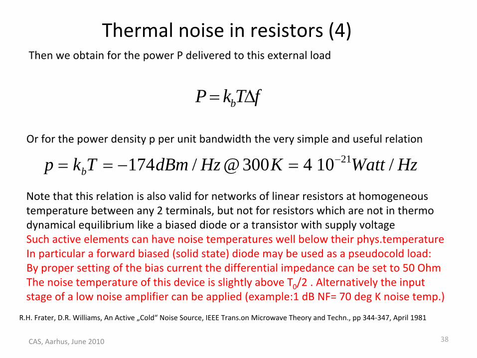
Thermal noise in resistors (4)Then we obtain for the power P delivered to this external load
fTkP b
HzWattKHzdBmTkp b /104300@/174 21
Or for the power density p per unit bandwidth the very simple and useful relation
Note that this relation is also valid for networks of linear resistors at homogeneoustemperature between any 2 terminals, but not for resistors which
are not in thermodynamical equilibrium like a biased diode or a transistor with supply voltageSuch active elements can have noise temperatures well below their phys.temperatureIn particular a forward biased (solid state) diode may be used as a pseudocold load:By proper setting of the bias current the differential impedance
can be set to 50 OhmThe noise temperature of this device is slightly above T0
/2 . Alternatively the input stage of a low noise amplifier can be applied (example:1 dB NF= 70 deg K noise temp.)
R.H. Frater, D.R. Williams, An Active „Cold“
Noise Source, IEEE Trans.on Microwave Theory and Techn., pp 344‐347, April 1981
38CAS, Aarhus, June 2010

Noise figure measurements (1)• The term “noise‐figure”
and “noise‐factor”
are used to describe the noise
properties of amplifiers. F is defined as signal to noise (power) ratio and the input
of the DUT versus signal to noise power ratio at the output. F is always >1 for
linear networks i.e. the signal to noise ratio at the output of some 2‐port or 4‐
pole
is always more or less degraded. In other words, the DUT (which may be also an
amplifier with a gain smaller than unity i.e. an attenuator)is always adding some of
its own noise to the signal.
• F[dB] is called “noise figure”• F[linear units of power ratio] sometimes noise factor• F[dB] = 10 log F[linear units]
with
• ENR stand for excess noise ratio delivered by the noise diode and tells us how
much “warmer”
than room temperature the noise diode appears. For an ENR of
16 dB this amounts roughly a factor of 40 in power or 40 times 300 K which is
12000 K.
• The quantity “Y “ is the ratio of noise power densities measured on the SPA
between the settings: noise source on and noise source off.
CAS, Aarhus, June 2010 39
11][][][
YTT
unitlinearYunitlinearENRunitlinearF
o
ex T T Tex H 0
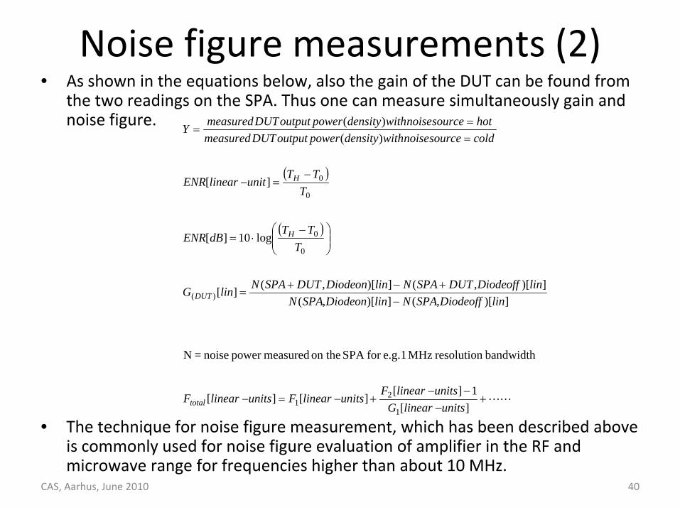
Noise figure measurements (2)• As shown in the equations below, also the gain of the DUT can be
found from
the two readings on the SPA. Thus one can measure simultaneously
gain and
noise figure.
• The technique for noise figure measurement, which has been described above
is commonly used for noise figure evaluation of amplifier in the
RF and
microwave range for frequencies higher than about 10 MHz.
CAS, Aarhus, June 2010 40
][1][][][
bandwidth resolution MHz 1 e.g.for SPA on the measuredpower noise = N
])[,(])[,(])[,(])[,(][
log10][
][
)()(
1
21
)(
0
0
0
0
unitslinearGunitslinearFunitslinearFunitslinearF
linoffDiodeSPANlinonDiodeSPANlinoffDiodeDUTSPANlinonDiodeDUTSPANlinG
TTT
dBENR
TTT
unitlinearENR
coldsourcenoisewithdensitypoweroutputDUTmeasuredhotsourcenoisewithdensitypoweroutputDUTmeasuredY
total
DUT
H
H
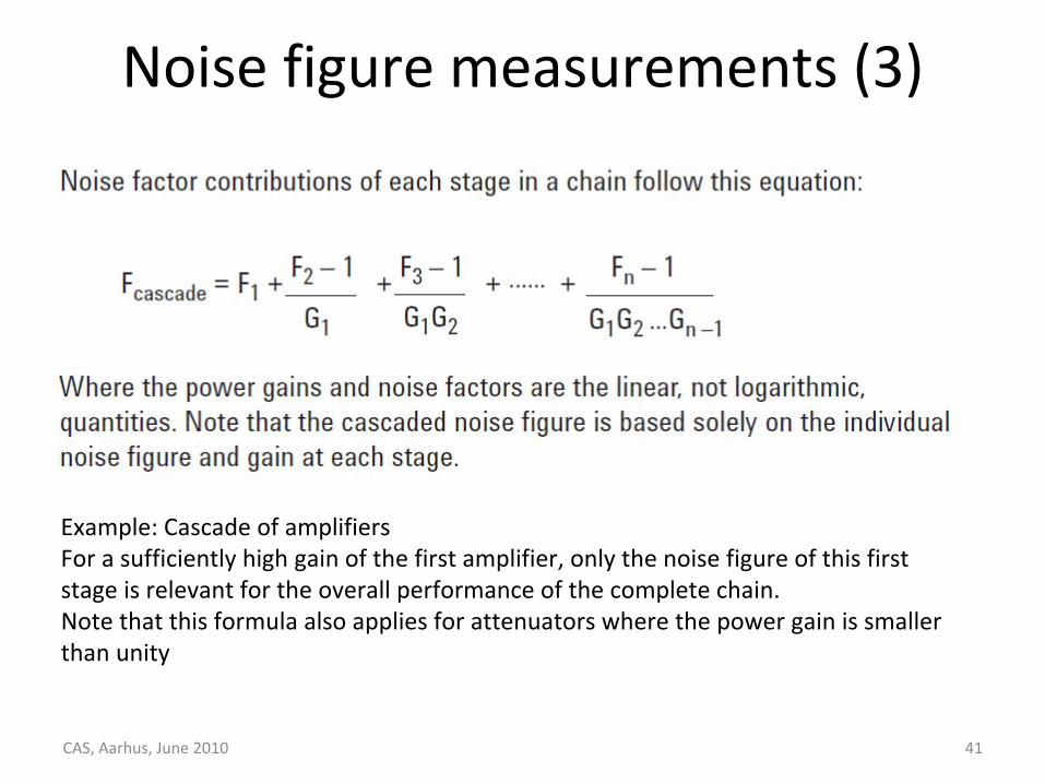
Noise figure measurements (3)
CAS, Aarhus, June 2010 41
Example: Cascade of amplifiersFor a sufficiently high gain of the first amplifier, only the noise figure of this first
stage is relevant for the overall performance of the complete chain. Note that this formula also applies for attenuators where the power gain is smaller
than unity
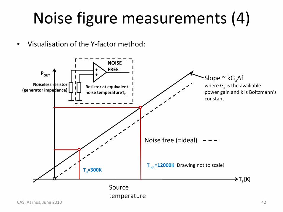
Noise figure measurements (4)• Visualisation
of the Y‐factor method:
CAS, Aarhus, June 2010 42
++
TS
[K]
NOISE
FREE
Noise free (=ideal)
Source
temperature
POUT Slope ~ kGa
Δfwhere Ga
is the availiable
power gain and k is Boltzmann’s
constant
T0
=300KThot
=12000K Drawing not to scale!
Resistor at equivalent
noise temperatureTE
Noiseless resistor
(generator impedance)

Noise figure measurements (5)• Practical application of the Y factor method:
• We obtain the gain of the DUT from the slope of the characteristic shown on
the last slide and the noise temperature from the intersection with the
negative horizontal axis
• Since we determine with the hot – cold method two points on a straight line
which defines unambiguously its position.
• In order to get clean measurements, we select the highest possible
resolution BW (3 or 5 MHz) on the SPA as well as a very low Video BW (10 Hz)
(smoothing of the trace) and a measurement time of about 1 second per
frequency point
• At each measurement point, we have to turn on and off the noise diode,
switching between 300 K and 12000K noise temperature
• Of course we would run this kind of measurements automatically, but for
trouble shooting or if this automatic function is not available,
we have to do
it manually.
CAS, Aarhus, June 2010 43