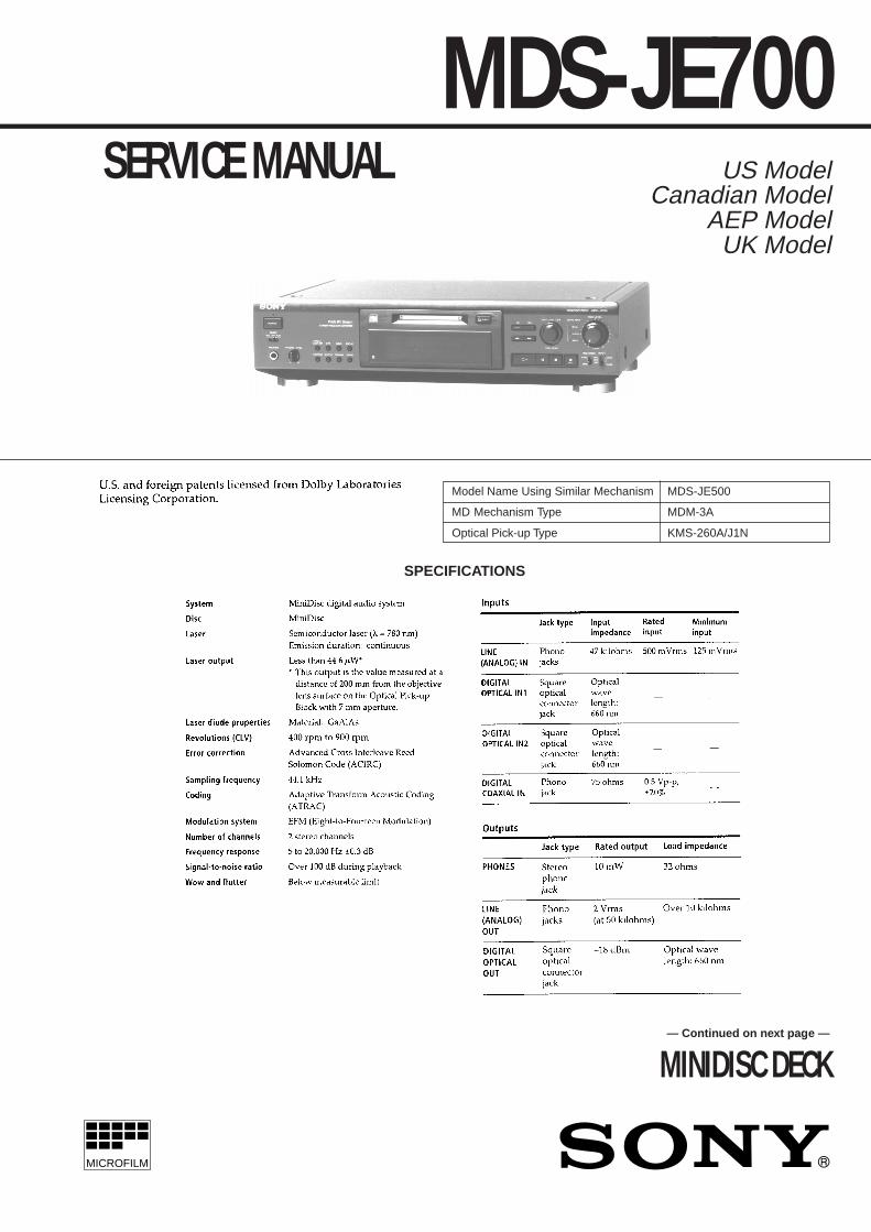
mds-je700 - · pdf filemodel name using similar mechanism mds-je500 md mechanism type mdm-3a...
TRANSCRIPT
— 1 —
Model Name Using Similar Mechanism MDS-JE500
MD Mechanism Type MDM-3A
Optical Pick-up Type KMS-260A/J1N
MDS-JE700SERVICE MANUAL US Model
Canadian ModelAEP Model
UK Model
MINIDISC DECK
MICROFILM
SPECIFICATIONS
— Continued on next page —
— 2 —
CAUTION
Danger of explosion if battery is incorrectly replaced.Replace only with the same or equivalent type recommended bythe equipment manufacturer.Discard used batteries according to manufacture’s instructions.
ADVARSEL!
Lithiumbatteri - Eksplosionsfare ved fejlagtig håndtering.Udskiftning må kun ske med batteri af samme fabrikat og type.
Levér det brugte batteri tilbage til leverandøren.
ADVARSEL
Eksplosjonsfare ved feilakting skifte av batteri.Benytt samme batteritype eller en tilsvarende type anbefalt av
apparatfabrikanten.Brukte batterier katterier kasseres i henhold til fabrikantens
VARNIG
Explosionsfara vid felaktigt batteribyte.Använd samma batterityp eller en likvärdig typ som rekommenderasav apparattillverkaren.Kassera använt batteri enligt gällande föreakrifter.
VAROITUS
Parist voi räjähtää, jos se on virheellisesti asennettu.Vaihda paristo ainoastaan laitevalmistajan suosittelemaan tyyppiin.Hävitä käytetty paristo valmistajan ohjeiden mukaisesti.
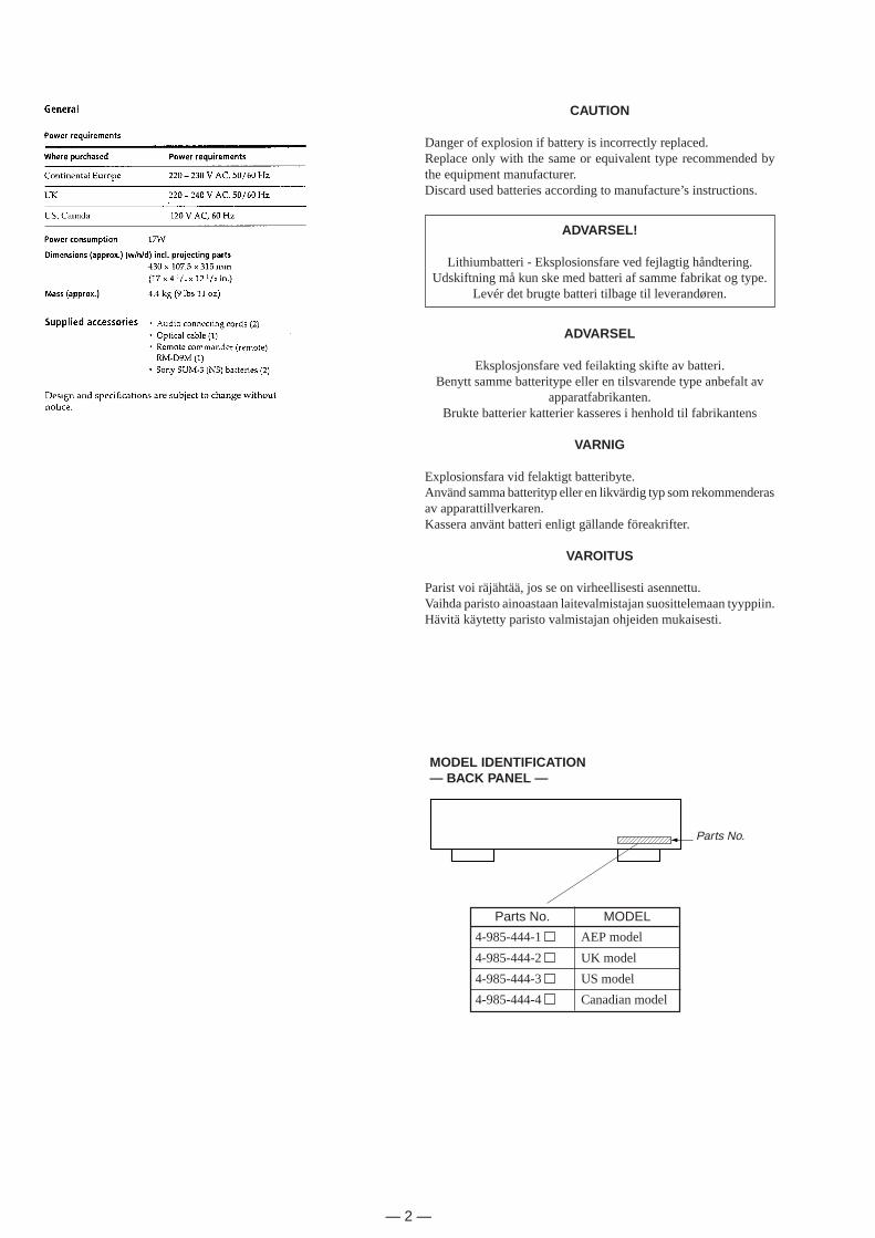
MODEL IDENTIFICATION— BACK PANEL —
Parts No.
4-985-444-1
4-985-444-2
4-985-444-3
4-985-444-4
Parts No. MODEL
AEP model
UK model
US model
Canadian model
— 3 —
Notes on chip component replacement• Never reuse a disconnected chip component.• Notice that the minus side of a tantalum capacitor may be
damaged by heat.
Flexible Circuit Board Repairing• Keep the temperature of soldering iron around 270˚C
during repairing.• Do not touch the soldering iron on the same conductor of the
circuit board (within 3 times).• Be careful not to apply force on the conductor when soldering
or unsoldering.
This appliance is classified as a CLASS 1LASER product. The CLASS 1 LASERPRODUCT MARKING is located on therear exterior.
The following caution label is locatedinside the unit.
CAUTIONUse of controls or adjustments or performance of proceduresother than those specified herein may result in hazardous ra-diation exposure.
The laser component in this product iscapable of emitting radiation exceedingthe limit for Class 1.
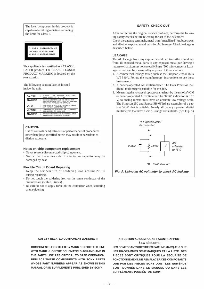
To Exposed MetalParts on Set
0.15µF 1.5kΩACvoltmeter(0.75V)
Earth Ground
SAFETY CHECK-OUT
After correcting the original service problem, perform the follow-ing safety checks before releasing the set to the customer:Check the antenna terminals, metal trim, “metallized” knobs, screws,and all other exposed metal parts for AC leakage. Check leakage asdescribed below.
LEAKAGEThe AC leakage from any exposed metal part to earth Ground andfrom all exposed metal parts to any exposed metal part having areturn to chassis, must not exceed 0.5 mA (500 microampers). Leak-age current can be measured by any one of three methods.1. A commercial leakage tester, such as the Simpson 229 or RCA
WT-540A. Follow the manufacturers’ instructions to use theseinstruments.
2. A battery-operated AC milliammeter. The Data Precision 245digital multimeter is suitable for this job.
3. Measuring the voltage drop across a resistor by means of a VOMor battery-operated AC voltmeter. The “limit” indication is 0.75V, so analog meters must have an accurate low-voltage scale.The Simpson 250 and Sanwa SH-63Trd are examples of a pas-sive VOM that is suitable. Nearly all battery operated digitalmultimeters that have a 2V AC range are suitable. (See Fig. A)
Fig. A. Using an AC voltmeter to check AC leakage.
SAFETY-RELATED COMPONENT WARNING !!
COMPONENTS IDENTIFIED BY MARK ! OR DOTTED LINE
WITH MARK ! ON THE SCHEMATIC DIAGRAMS AND IN
THE PARTS LIST ARE CRITICAL TO SAFE OPERATION.
REPLACE THESE COMPONENTS WITH SONY PARTSWHOSE PART NUMBERS APPEAR AS SHOWN IN THIS
MANUAL OR IN SUPPLEMENTS PUBLISHED BY SONY.
ATTENTION AU COMPOSANT AYANT RAPPORT À LA SÉCURITÉ!!
LES COMPOSANTS IDENTIFIÉS PAR UNE MARQUE ! SUR
LES DIAGRAMMES SCHÉMATIQUES ET LA LISTE DES
PIÈCES SONT CRITIQUES POUR LA SÉCURITÉ DE
FONCTIONNEMENT. NE REMPLACER CES COMPOSANTS
QUE PAR DES PIÈCES SONY DONT LES NUMÉROS
SONT DONNÉS DANS CE MANUEL OU DANS LES
SUPPLÉMENTS PUBLIÉS PAR SONY.
— 4 —
TABLE OF CONTENTS
1. SERVICING NOTE .......................................................... 5
2. GENERAL .......................................................................... 8
3. DISASSEMBLY3-1. Case and Front Panel Assembly .......................................... 243-2. Bracket (T), (L) and (R) ...................................................... 243-3. BD Board ........................................................................... 253-4. SUB Chassis ........................................................................ 253-5. Shutter Assembly ................................................................ 263-6. Over Write Head ................................................................. 263-7. Slider Complete Assembly .................................................. 27
4. TEST MODE ..................................................................... 28
5. ELECTRICAL ADJUSTMENTS ............................... 31
6. DIAGRAMS6-1. Circuit Boards Location ...................................................... 366-2. Brock Diagrams
• BD Section ....................................................................... 37• Main Section .................................................................... 39
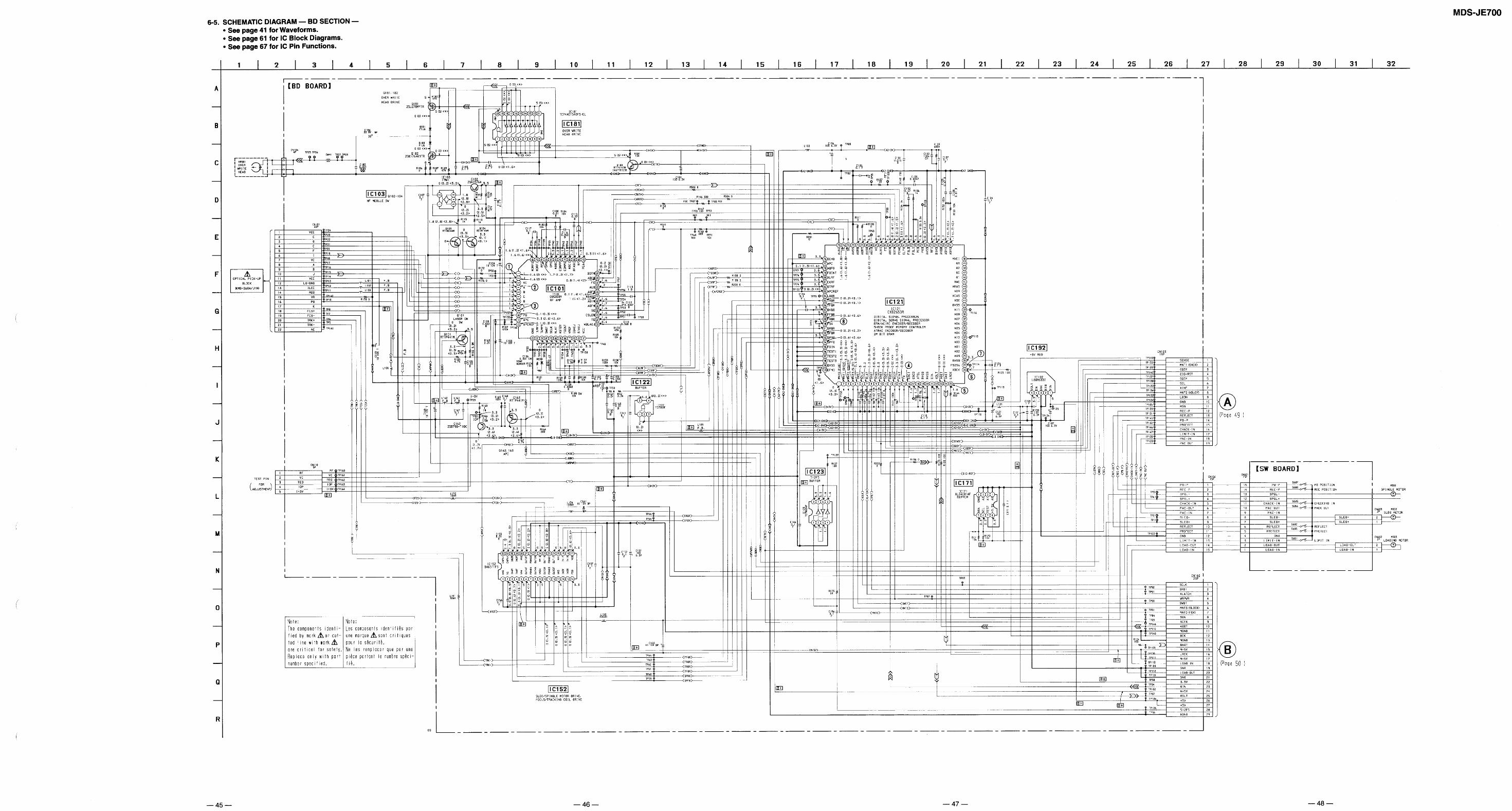
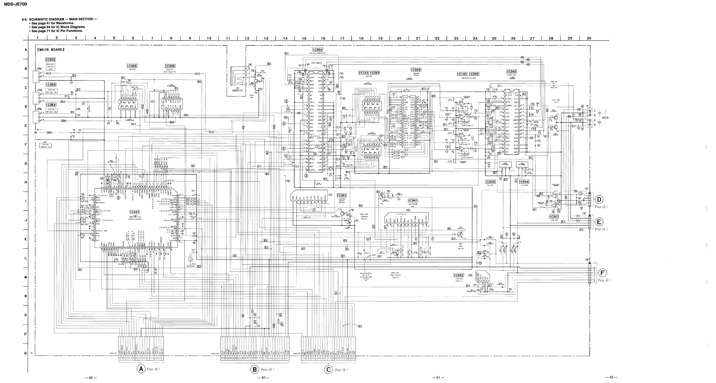
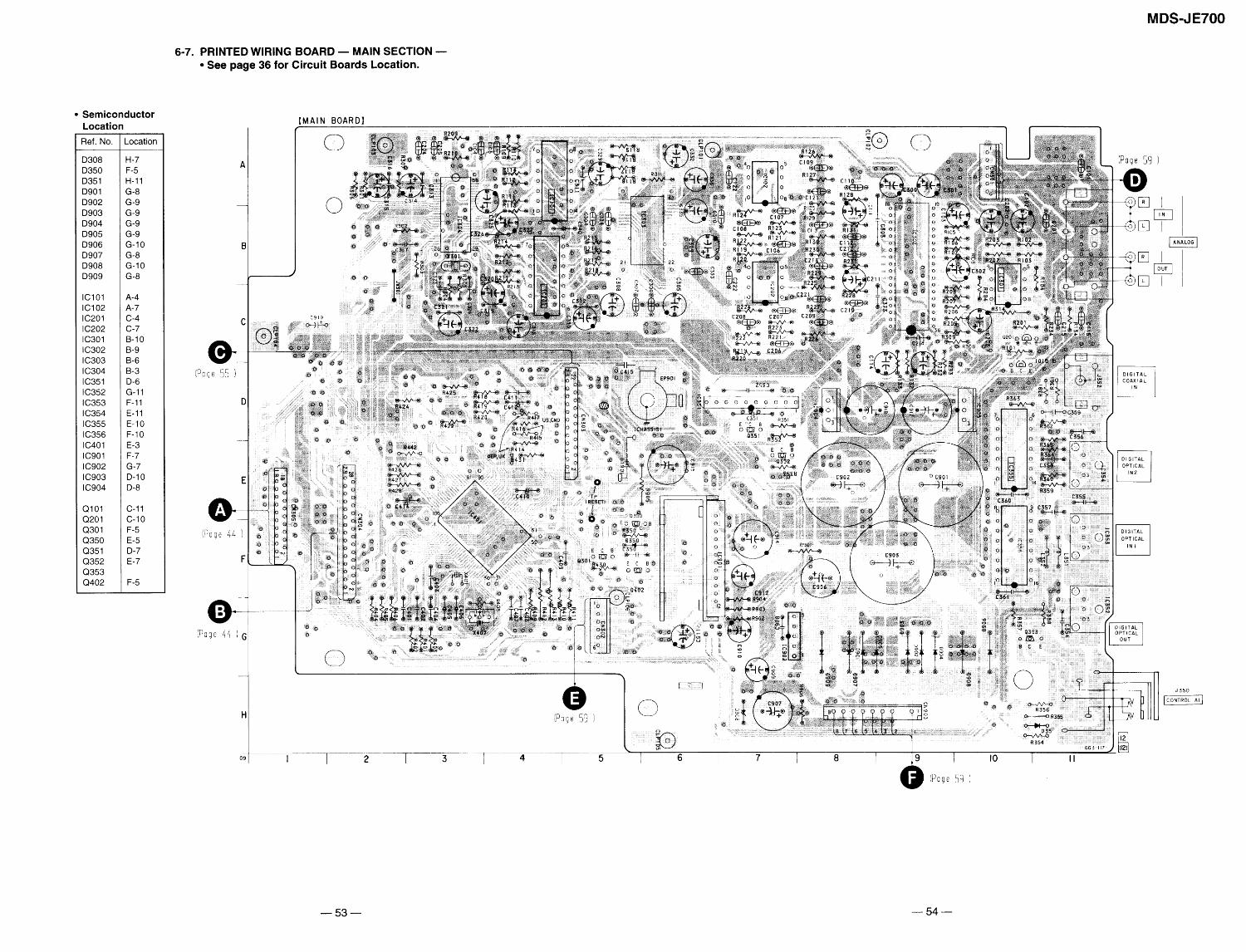
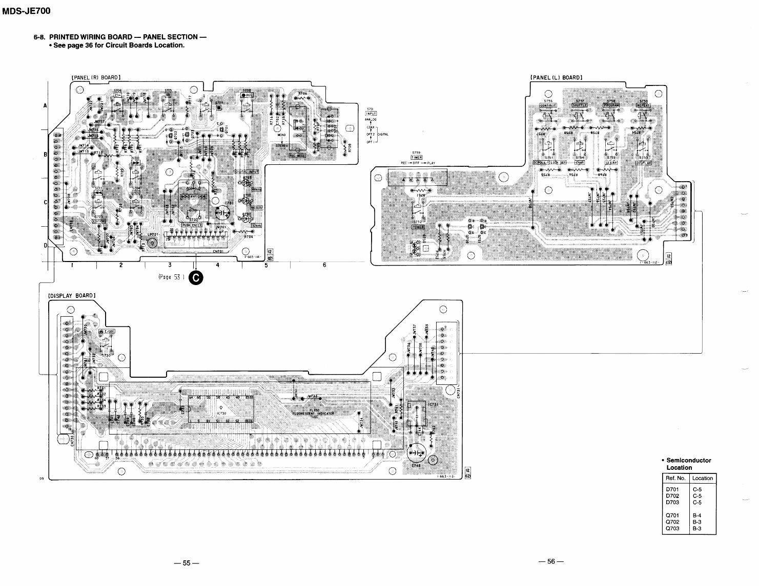
6-3. Waveforms ......................................................................... 416-4. Printed Wiring Board — BD Section —............................. 436-5. Schematic Diagram — BD Section — ............................... 456-6. Schematic Diagram — Main Section — ............................ 496-7. Printed Wiring Board — Main Section —.......................... 536-8. Printed Wiring Board — Panel Section — ......................... 556-9. Schematic Diagram — Panel Section — ............................ 576-10. Printed Wiring Board — HP Section — .......................... 596-11. Schematic Diagram — HP Section — ............................. 606-12. IC Block Diagrams ........................................................... 616-13. IC Pin Functions ............................................................... 67
7. EXPLODED VIEWS7-1. Case and Main Board Section ............................................. 767-2. Front Panel Section ............................................................. 777-3. Mechanism Deck Section (1) (MDM-3A) .......................... 787-4. Mechanism Deck Section (2) (MDM-3A) .......................... 79
8. ELECTRICAL PARTS LIST ........................................ 80
— 5 —
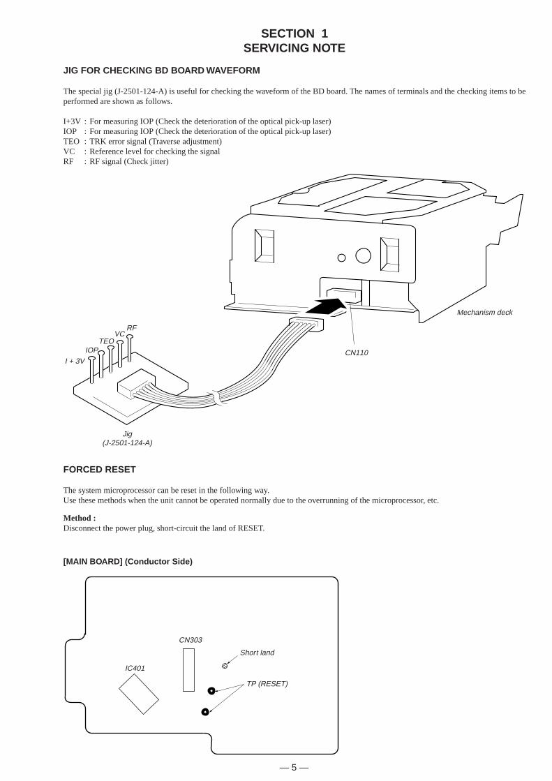
SECTION 1SERVICING NOTE
JIG FOR CHECKING BD BOARD WAVEFORM
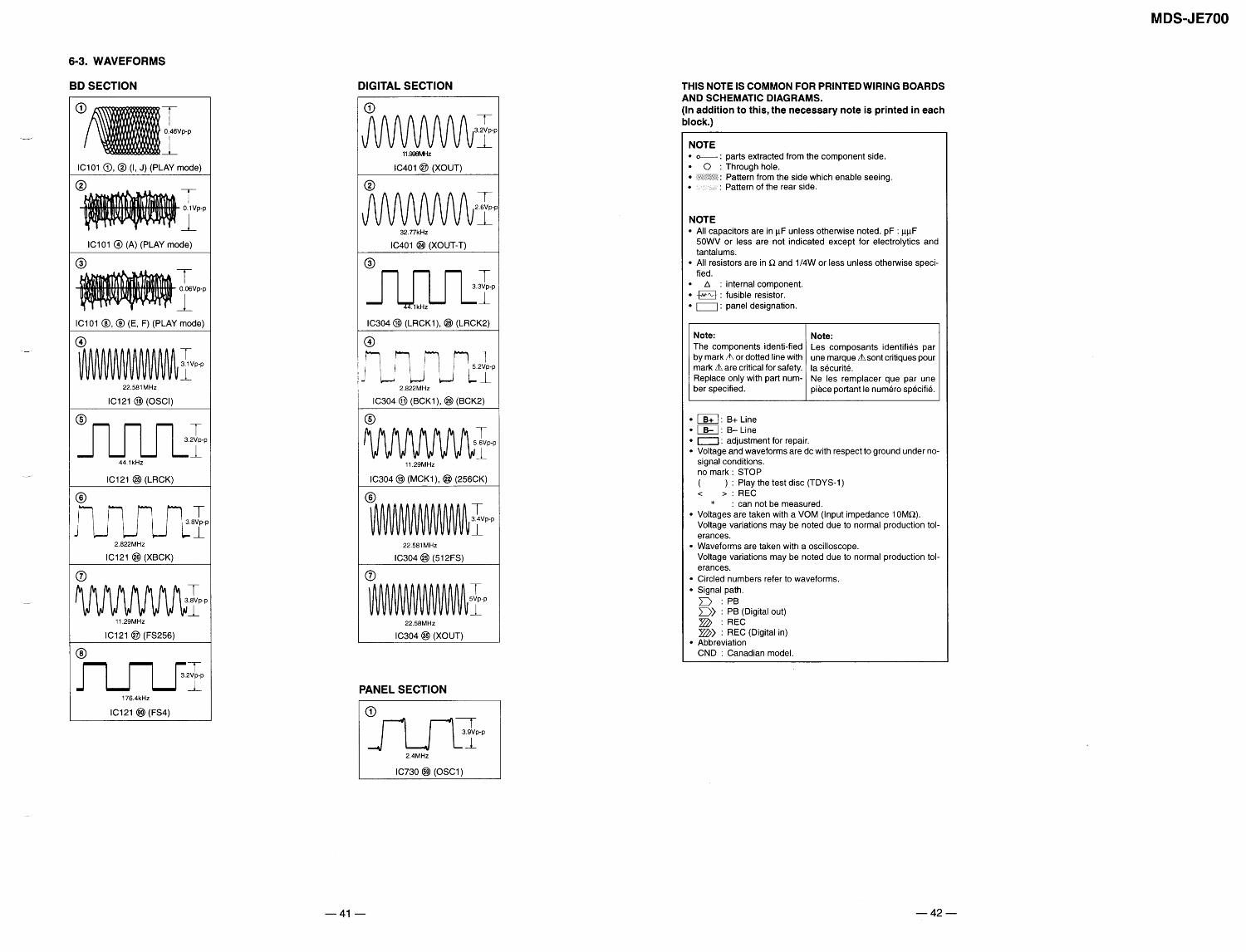
The special jig (J-2501-124-A) is useful for checking the waveform of the BD board. The names of terminals and the checking items to beperformed are shown as follows.
I+3V : For measuring IOP (Check the deterioration of the optical pick-up laser)IOP : For measuring IOP (Check the deterioration of the optical pick-up laser)TEO : TRK error signal (Traverse adjustment)VC : Reference level for checking the signalRF : RF signal (Check jitter)
FORCED RESET
The system microprocessor can be reset in the following way.Use these methods when the unit cannot be operated normally due to the overrunning of the microprocessor, etc.
IOPI + 3V
TEOVC
RF
Mechanism deck
CN110
Jig(J-2501-124-A)
Method :Disconnect the power plug, short-circuit the land of RESET.
[MAIN BOARD] (Conductor Side)
Short land
TP (RESET)
CN303
IC401
— 6 —
RETRY CAUSE DISPLAY MODE
• In this test mode, the causes for retry of the unit during recording can be displayed on the fluorescent display tube.This is useful for locating the faulty part of the unit.
• The data amount stored in D RAM, number of retries, and retry cause are displayed. Each is displayed in hexadecimal number.• The display of the D RAM data amount enables data reading, accumulation, ejection, and writing to be performed smoothly. If writing is
not smooth, data may decrease considerably.
Method:1. Load a recordable disc whose contents can be erased into the unit.2. Press the EDIT/NO button several times to display “All Erase?” on the fluorescent display tube.3. Press the YES button.4. When “All Erase??” is displayed on the fluorescent display tube, the numbers on the music calendar will start blinking.5. Press the YES button to display “Complete”, and press the p button immediately and continue pressing for about 10 seconds.6. When the “TOC” displayed on the fluorescent display tube goes off, release the p button.7. Press the r REC button to start recording.8. Press the DISPLAY button to display the test mode (Fig. 1), and check the display.9. The Rt value increases with each retry. If an error occurs after a retry, “Retry Error” will be displayed, and the number of retries counted
will be set back to 0.10. To exit the test mode, press the POWER button. Turn OFF the power, and after “TOC” disappears, disconnect the power plug from the
outlet.
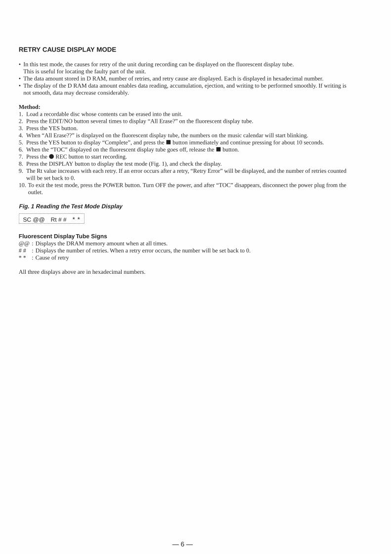
Fig. 1 Reading the Test Mode Display
SC @@ Rt # # ∗ ∗
Fluorescent Display Tube Signs@@ : Displays the DRAM memory amount when at all times.# # : Displays the number of retries. When a retry error occurs, the number will be set back to 0.* * : Cause of retry
All three displays above are in hexadecimal numbers.
— 7 —
Reading the Retry Cause Display
Hexadecimal
Bit
Binary
Higher Bits Lower Bits
8 4 2 1 8 4 2 1
b7 b6 b5 b4 b3 b2 b1 b0
0 0 0 0 0 0 0 0
0 0 0 0 0 0 0 1
0 0 0 0 0 0 1 0
0 0 0 0 0 1 0 0
0 0 0 0 1 0 0 0
0 0 0 1 0 0 0 0
0 0 1 0 0 0 0 0
0 1 0 0 0 0 0 0
1 0 0 0 0 0 0 0
When spindle rotation is detected as slow
When more than 3.5 shocks are detected
When ADER was counted more than
five times continuously
When ADIP address is not continuous
(Not used)
When not in focus
When ABCD signal level exceeds the specified range
When CLV is unlocked
When access operation is not performed normally
Hexa-
decimal
Spindle is slow
shock *1
ader5
Discontinuous address
(Not used)
FCS incorrect
IVR rec error
CLV unlock
Access fault
Cause of Retry Occurring conditions
00
01
02
04
08
10
20
40
80
*1 Some displays are not used depending on the microprocessor version.
Reading the Display:Convert the hexadecimal display into binary display. If more than two causes, they will be added.
ExampleWhen 42 is displayed:Higher bit : 4 = 0100 n b6Lower bit : 2 = 0010 n b1In this case, the retry cause is combined of “CLV unlock” and “ader5”.
When A2 is displayed:Higher bit : A = 1010 n b7+b5Lower bit : 2 = 0010 n b1
The retry cause in this case is combined of “access fault”, “IVR rec error”, and “ader5”.
Hexadecimal n Binary Conversion Table
Hexadecimal Binary Hexadecimal Binary
0
1
2
3
4
5
6
7
8
9
A
B
C
D
E
F
0000
0001
0010
0011
0100
0101
0110
0111
1000
1001
1010
1011
1100
1101
1110
1111
— 8 —
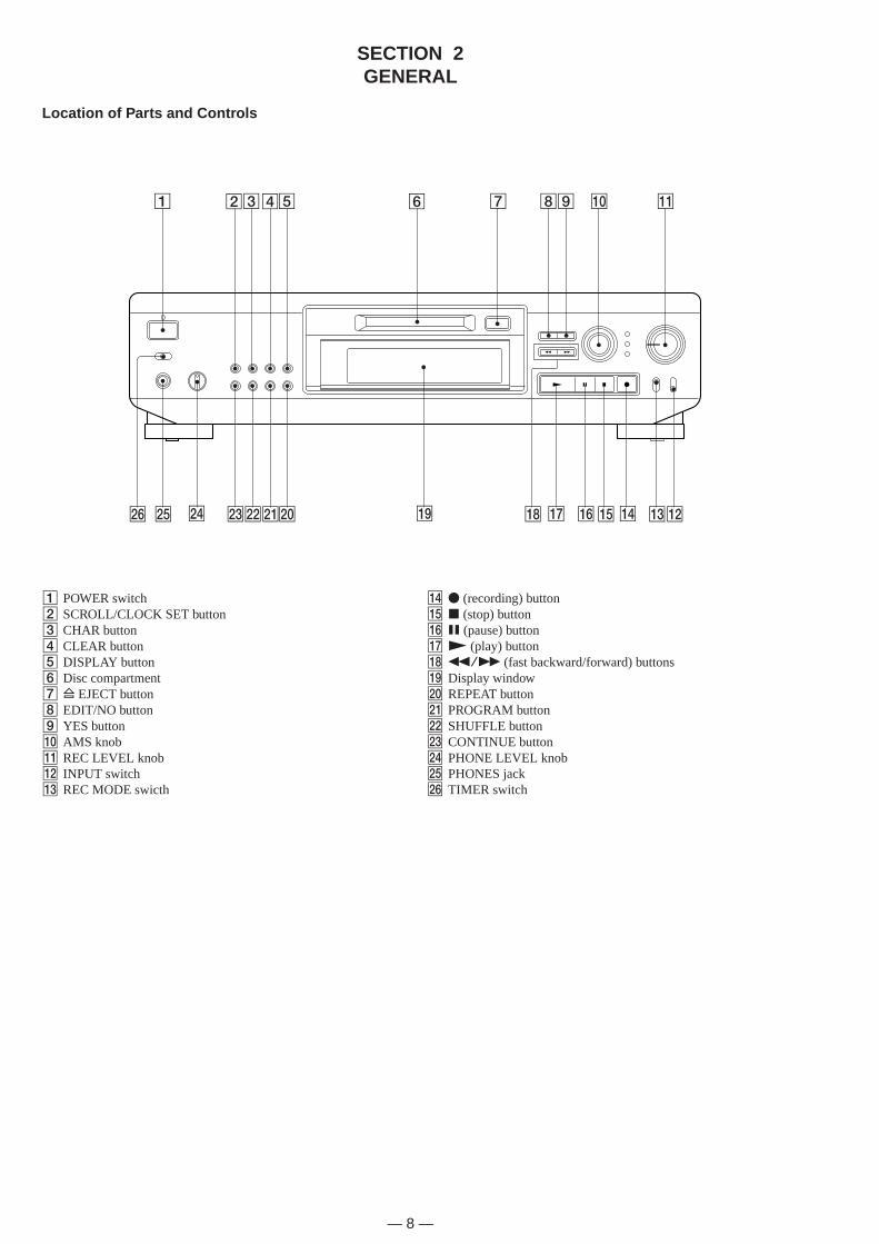
SECTION 2GENERAL
Location of Parts and Controls
1 2345 6 7 89 0 !¡
!™!£!¢!∞!§!¶!•!ª@º@¡@™@£@¢@∞@§
1 POWER switch2 SCROLL/CLOCK SET button3 CHAR button4 CLEAR button5 DISPLAY button6 Disc compartment7 § EJECT button8 EDIT/NO button9 YES button!º AMS knob!¡ REC LEVEL knob!™ INPUT switch!£ REC MODE swicth
!¢ r (recording) button!∞ p (stop) button!§ P (pause) button!¶( (play) button!•0/) (fast backward/forward) buttons!ª Display window@º REPEAT button@¡ PROGRAM button@™ SHUFFLE button@£ CONTINUE button@¢ PHONE LEVEL knob@∞ PHONES jack@§ TIMER switch
— 9 —
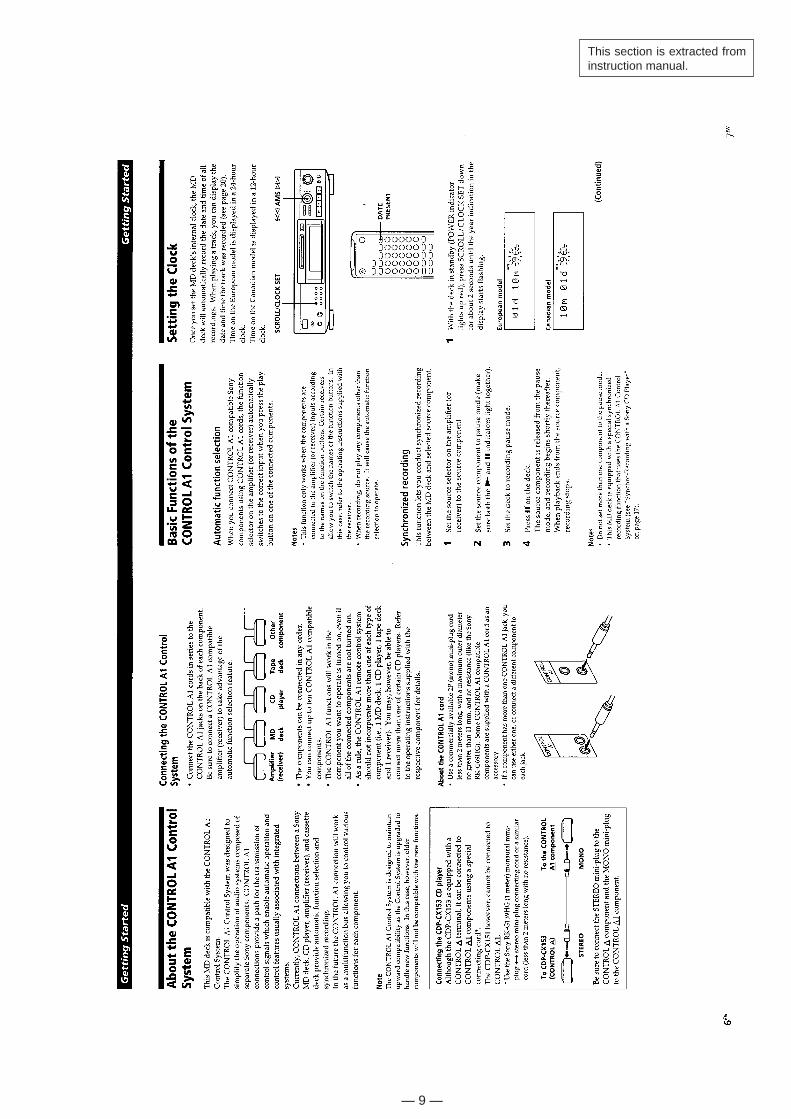
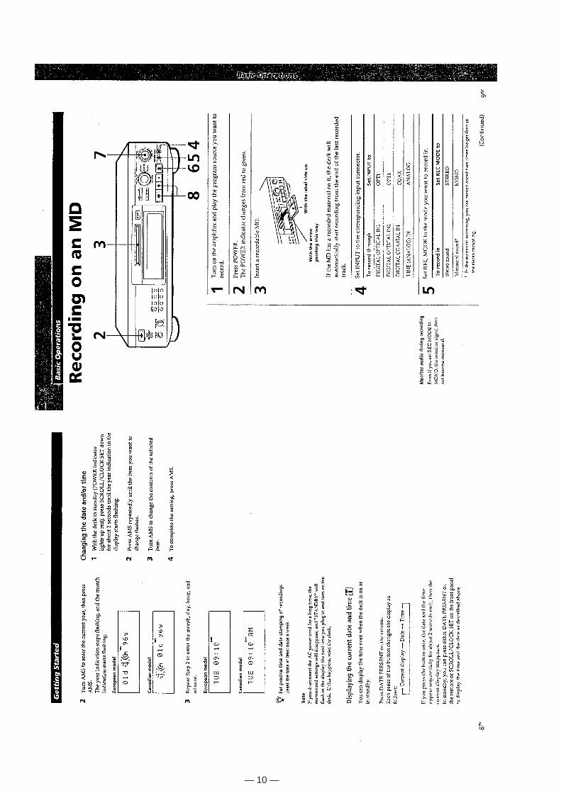
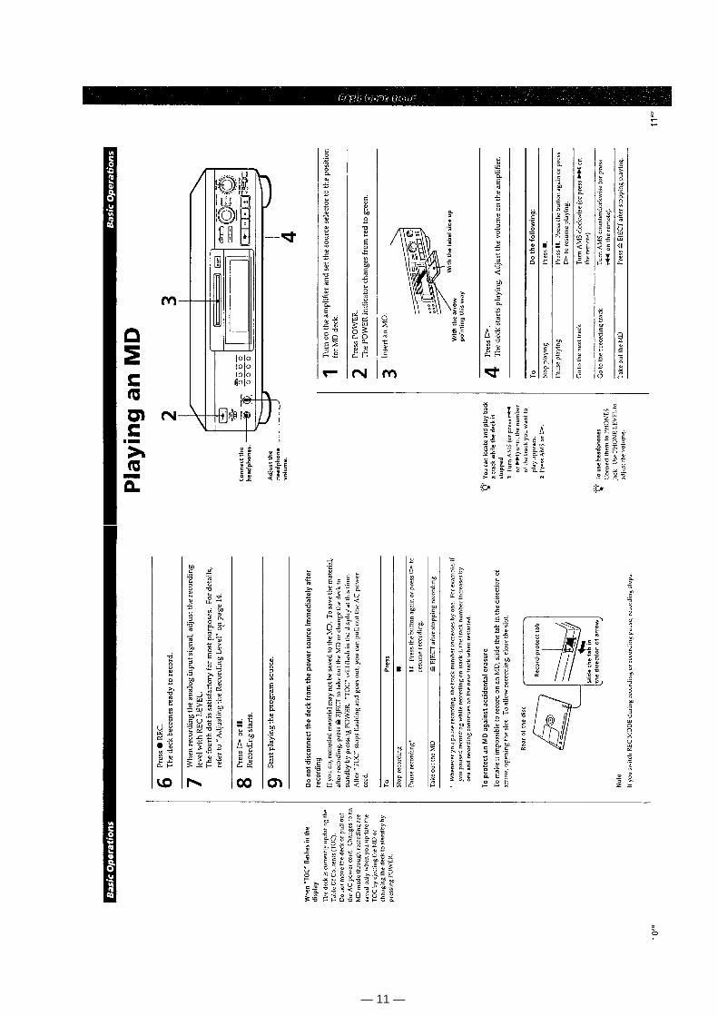
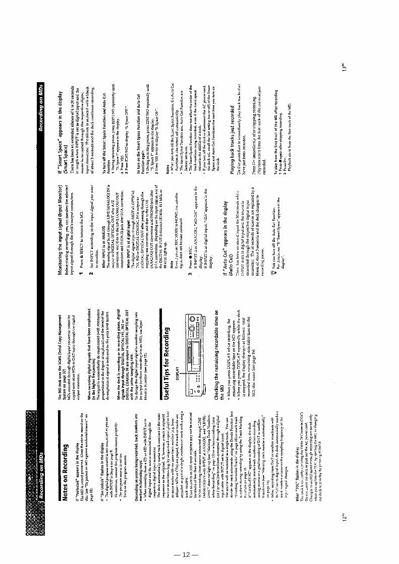
This section is extracted frominstruction manual.
— 10 —
— 11 —
— 12 —
— 13 —
— 14 —
— 15 —
— 16 —
— 17 —
— 18 —
— 19 —
— 20 —
— 21 —
— 22 —
— 23 —
— 24 —
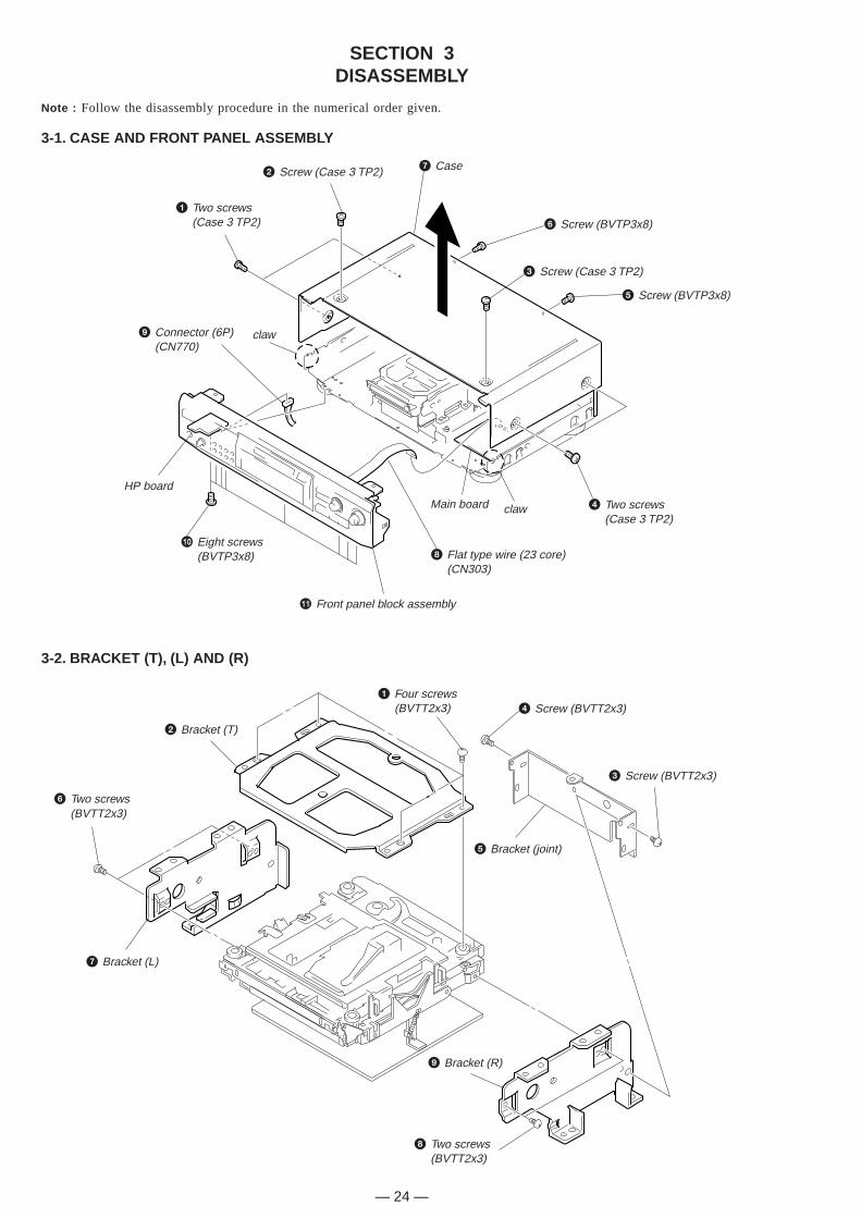
SECTION 3DISASSEMBLY
Note : Follow the disassembly procedure in the numerical order given.
3-1. CASE AND FRONT PANEL ASSEMBLY
1 Two screws(Case 3 TP2)
2 Screw (Case 3 TP2)
6 Screw (BVTP3x8)
7 Case
3-2. BRACKET (T), (L) AND (R)
1 Four screws(BVTT2x3)
2 Bracket (T)
3 Screw (BVTT2x3)
4 Screw (BVTT2x3)
5 Bracket (joint)
6 Two screws(BVTT2x3)
7 Bracket (L)
9 Bracket (R)
8 Two screws(BVTT2x3)
3 Screw (Case 3 TP2)
4 Two screws(Case 3 TP2)
5 Screw (BVTP3x8)
8 Flat type wire (23 core)(CN303)
9 Connector (6P)(CN770)
0 Eight screws(BVTP3x8)
!¡ Front panel block assembly
Main board claw
HP board
claw
— 25 —
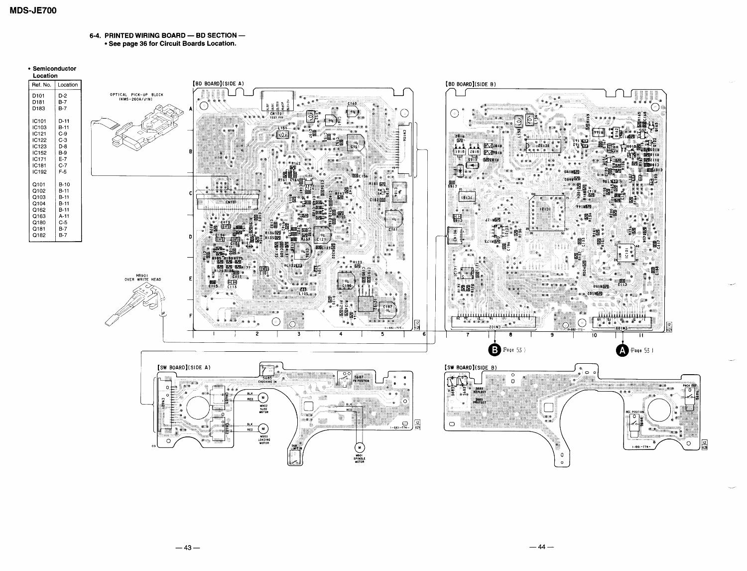
3-3. BD BOARD
3-4. SUB CHASSIS
1 Flexible board(Over write head)
2 Flat type wire (15 core)
3 Screw (BVTT2x4)
4 OP relay flexible board
5 BD board
1 Two step screws
2 Two step screws3 Two insulators
4 Two insulators
5 Sub chassis
Part A
Part A
Part A
NG
OK
Take care so that the part Amay be right position when installing.
— 26 —
3-5. SHUTTER ASSEMBLY
3-6. OVER WRITE HEAD
1 Stopper washer
2 Shaft (shutter)
3 Shutter assembly
Shaft (lid)
Shaft (shutter)Hole B
Hole A
When installing, install the shaft(shutter) into the hole as shownin the figure before installing theshaft (lid) into the hole B.
1 Precision screw (P1.7x6)
2 Over write head
Shutter assembly
— 27 —
3-7. SLIDER COMPLETE ASSEMBLY
1 Screw(M1.7x2) 2 Retainer (gear)
3 Set the shaft of Gear (LB) to be at theposition in the figure.
4 Remove the slider complete assemblyin the direction of arrow with puttingout of two claws.
claw
claw
45°
Slider assembly
OK
NG
Take care not to damagethe detective switch.
Part A
Install the part A of lever (head up)to pass over the slider complete assembly.
• Note for Installation of Slider Complete Assembly
— 28 —
SECTION 4TEST MODE
4-1. PRECAUTIONS FOR USE OF TEST MODE1 As loading related operations will be performed regardless of the test mode operations being performed, be sure to check that the disc is
stopped before setting and removing it.Even if the §EJECT button is pressed while the disc is rotating during continuous playback, continuous recording, etc., the disc will notstop rotating.Therefore, it will be ejected while rotating.Be sure to press the §EJECT button after pressing the NO button and the rotation of disc is stopped.
2 The erasing-protection tab is not detected in the test mode. Therefore, operating in the recording laser emission mode and pressing therREC button, the recorded contents will be erased regardless of the position of the tab. When using a disc that is not to be erased in thetest mode, be careful not to enter the continuous recording mode and traverse adjustment mode.
4-1-1. Recording laser emission mode and operating buttons
1. Continuous recording mode (CREC MODE)2. Traverse adjustment mode (EFBAL ADJUST)3. Laser power adjustment mode (LDPWR ADJUST)4. Laser power check mode (LDPWR CHECK)5. When pressing the rREC button.
4-2. SETTING THE TEST MODEWhile pressing the AMS knob, insert the power plug into the power supply inlet, and release the AMS knob.
4-3. EXITING THE TEST MODEWhen the REPEAT button is pressed, it becomes in the STANDBY mode. Or unplug the power plug from an outlet.
4-4. BASIC OPERATIONS OF THE TEST MODEAll operations are performed using the AMS knob, YES button, and NO button.The functions of these buttons are as follows.
Function name
AMS knob
YES button
NO button
Function
Changes parameters and modes
Proceeds onto the next step. Finalizes input.
Returns to previous step. Stops operations.
4-5. SELECTING THE TEST MODEThirteen test modes are selected by turning the AMS knob.
Display
TEMP ADJUST
LDPWR ADJUST
LDPWR CHECK
EFBAL ADJUST
FBIAS ADJUST
FBIAS CHECK
CPLAY MODE
CREC MODE
DETRK CHECK
S curve CHECK
EEP MODE
MANUAL CMD
SVDATA READ
Contents
Temperature compensation offset adjustment
Laser power adjustment
Laser power check
Traverse adjustment
Focus bias adjustment
Focus bias check
Continuous playback mode
Continuous recording mode
Detrack check
S curve check ∗
Non-volatile memory mode ∗
Manual command transfer mode ∗
Data reading out mode ∗
For detailed description of each adjustment mode, refer to “5. Electrical Adjustments”.If a different adjustment mode has been selected by mistake, press the NO button to exit from this mode.* The EEP MODE, S curve CHECK, MANUAL CMD and SVDATA READ are not used in servicing. If set accidentally, press the NO button
immediately to exit this mode.
— 29 —
4
4
4-5-1. Operating the Continuous Playback Mode
1. Entering the continuous playback mode1Set the disc in the unit. (Whichever recordable discs or discs for playback only are available.)2Rotate the AMS knob and display “CPLAY MODE”.3Press the YES button to change the display to “CPLAY IN”.4When access completes, the display changes to “C1 = AD = ”.Note : The numbers “” displayed show you error rates and ADER.
2. Changing the parts to be played back1Press the YES button during continuous playback to change the display as below.
“CPLAY MID” n “CPLAY OUT”n “CPLAY IN”
When pressed another time, the parts to be played back can be moved.2When access completes, the display changes to “C1 = AD = ”.Note : The numbers “” displayed show you error rates and ADER.
3. Ending the continuous playback mode1Press the NO button. The display will change to “CPLAY MODE”.2Press the §EJECT button to remove the disc.Note : The playback start addresses for IN, MID, and OUT are as follows. In case you want to display the address of the playback position
on the display, press the DISPLAY button and display “CPLAY ( )”.IN 40h clusterMID 300h clusterOUT 700h cluster
4-5-2. Operating the Continuous Recording Mode1. Entering the continuous recording mode1Set a recordable disc in the unit. (Refer to Note 3)2Rotate the AMS knob and display “CREC MODE”.3Press the YES button to change the display to “CREC MID”.4When access completes, the display changes to “CREC ()” and REC lights up.Note : The numbers “” displayed shows you the recording position addresses.
2. Changing the parts to be recorded1When the YES button is pressed during continuous recording, the display changes as below.
“CPLAY MID” n “CPLAY OUT”n “CPLAY IN”
When pressed another time, the parts to be recorded can be changed. REC goes off.2When access completes, the display changes to “CREC ()” and REC lights up.Note : The numbers “” displayed shows you the recording position addresses.
3. Ending the continuous recording mode1Press the NO button. The display changes to “CREC MODE” and REC goes off.2Press the §EJECT button to remove the disc.Note 1 : The recording start addresses for IN, MID, and OUT are as follows.
IN 40h clusterMID 300h clusterOUT 700h cluster
Note 2 :The NO button can be used to stop recording anytime.Note 3 :During the test mode, the erasing-protection tab will not be detected. Therefore be careful not to set the continuous recording
mode when a disc not to be erased is set in the unit.Note 4 :Do not perform continuous recording for long periods of time above 5 minutes.Note 5 :During continuous recording, be careful not to apply vibration.
4-5-3. Non-Volatile Memory ModeThis mode reads and writes the contents of the non-volatile memory.It is not used in servicing. If set accidentally, press the NO button immediately to exit it.
— 30 —
4-6. FUNCTIONS OF OTHER BUTTONS
¢
Contents
Sets continuous playback when pressed in the STOP state. When pressed during continuous playback, the tracking servo turns ON/OFF.
Stops continuous playback and continuous recording.
The sled moves to the outer circumference only when this is pressed.
The sled moves to the inner circumference only when this is pressed.
Turns recording ON/OFF when pressed during continuous playback.
Switches between the pit and groove modes when pressed.
Switches the spindle servo mode (CLVS and A).
Switches the display when pressed.Returns to previous step. Stops operations.
Function
p
)
0
r REC
SCROLL
PLAY MODE
DISPLAY
P
REC
CLOCK
TRACK
DISC
DATE
A. SPACE
A – B
Off Blinking
ContentsDisplay
Light
During continuous playback
Tracking servo OFF
Recording mode ON
CLV LOCK
Pit
High reflection
CLV-S
ABCD adjustment completed
STOP
Tracking servo ON
Recording mode OFF
CLV UNLOCK
Groove
Low reflection
CLV-A
Focus auto gain successful
Tracking auto gain successful
Focus auto gain successful
Tracking auto gain failed
¢
Note : The erasing-protection tab is not detected during the test mode. Recording will start regardless of the position of the erasing-protec-tion tab when the r REC button is pressed.
4-7. TEST MODE DISPLAYSEach time the DISPLAY button is pressed, the display changes in the following order.MODE displaynError rate displaynAddress displaynAuto gain displaynIVR displayThe auto gain display and the IVR display are not used for servicing.1. MODE display
Displays “TEMP ADJUST”, “CPLAY MODE”, etc.2. Error rate display
Error rates are displayed as follows.C1 = AD = C1 = : Indicates C1 errorAD= : Indicates ADER
3. Address displayAddresses are displayed as follows. (MO : Recordable disc, CD : Disc for playback only)h= s = (MO pit and CD)h= a = (MO groove)h= : Header addresss = : SUBQ addressa = : ADIP address* “_” is displayed when the address cannot be read.
4. Auto gain displayAuto gains are displayed as follows.AG F = T = F= Focus auto gain collection value.T= Tracking auto gain collection value.
4-8. MEANINGS OF OTHER DISPLAYS
— 31 —
SECTION 5ELECTRICAL ADJUSTMENTS
5-1. PRECAUTIONS FOR CHECKING LASER DIODEEMISSINON
To check the emission of the laser diode during adjustments, neverview directly from the top as this may lose your eye-sight.
5-2. PRECAUTIONS FOR USE OF OPTICAL PICK-UP (KMS-260A)
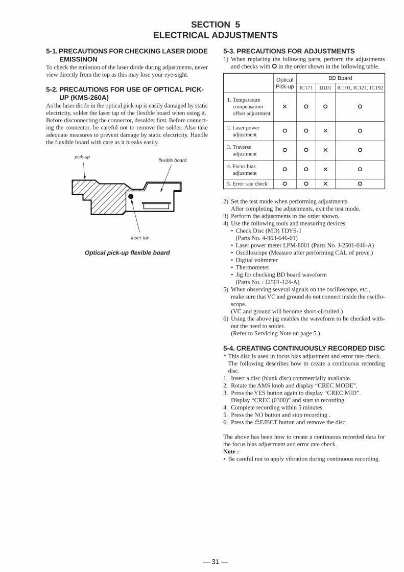
As the laser diode in the optical pick-up is easily damaged by staticelectricity, solder the laser tap of the flexible board when using it.Before disconnecting the connector, desolder first. Before connect-ing the connector, be careful not to remove the solder. Also takeadequate measures to prevent damage by static electricity. Handlethe flexible board with care as it breaks easily.
laser tap
flexible boardpick-up
Optical pick-up flexible board
5-3. PRECAUTIONS FOR ADJUSTMENTS1) When replacing the following parts, perform the adjustments
and checks with ¬ in the order shown in the following table.
1. Temperaturecompensationoffset adjustment
2. Laser poweradjustment
3. Traverseadjustment
4. Focus biasadjustment
OpticalPick-up
BD Board
IC101, IC121, IC192D101IC171
¬
¬
¬
¬
¬
G
¬
¬
¬
¬
¬
G
G
G
G
¬
¬
¬
¬
¬5. Error rate check
2) Set the test mode when performing adjustments.After completing the adjustments, exit the test mode.
3) Perform the adjustments in the order shown.4) Use the following tools and measuring devices.
• Check Disc (MD) TDYS-1(Parts No. 4-963-646-01)
• Laser power meter LPM-8001 (Parts No. J-2501-046-A)• Oscilloscope (Measure after performing CAL of prove.)• Digital voltmeter• Thermometer• Jig for checking BD board waveform
(Parts No. : J2501-124-A)5) When observing several signals on the oscilloscope, etc.,
make sure that VC and ground do not connect inside the oscillo-scope.(VC and ground will become short-circuited.)
6) Using the above jig enables the waveform to be checked with-out the need to solder.(Refer to Servicing Note on page 5.)
5-4. CREATING CONTINUOUSLY RECORDED DISC* This disc is used in focus bias adjustment and error rate check.
The following describes how to create a continuous recordingdisc.
1. Insert a disc (blank disc) commercially available.2. Rotate the AMS knob and display “CREC MODE”.3. Press the YES button again to display “CREC MID”.
Display “CREC (0300)” and start to recording.4. Complete recording within 5 minutes.5. Press the NO button and stop recording .6. Press the §EJECT button and remove the disc.
The above has been how to create a continuous recorded data forthe focus bias adjustment and error rate check.Note :• Be careful not to apply vibration during continuous recording.
— 32 —
5-5. TEMPERATURE COMPENSATION OFFSETADJUTMENT
Save the temperature data at that time in the non-volatile memoryas 25 ˚C reference data.Note :1. Usually, do not perform this adjustment.2. Perform this adjustment in an ambient temperature of 22 ˚C to
28 C. Perform it immediately after the power is turned on whenthe internal temperature of the unit is the same as the ambienttemperature of 22 ˚C to 28 ˚C.
3. When D101 has been replaced, perform this adjustment afterthe temperature of this part has become the ambient tempera-ture.
Adjusting Method :1. Rotate the AMS knob and display “TEMP ADJUST”.2. Press the YES button and select the “TEMP ADJUST” mode.3. “TEMP = ” and the current temperature data will be displayed.4. To save the data, press the YES button.
When not saving the data, press the NO button.5. When the YES button is pressed, “TEMP = SAVE” will be
displayed and turned back to “TEMP ADJUST” display then.When the NO button is pressed, “TEMP ADJUST” will be dis-played immediatelly.
Specified Value :The “TEMP = ” should be within “E0 - EF”, “F0 - FF”, “00 -0F”, “10 - 1F” and “20 - 2F”.
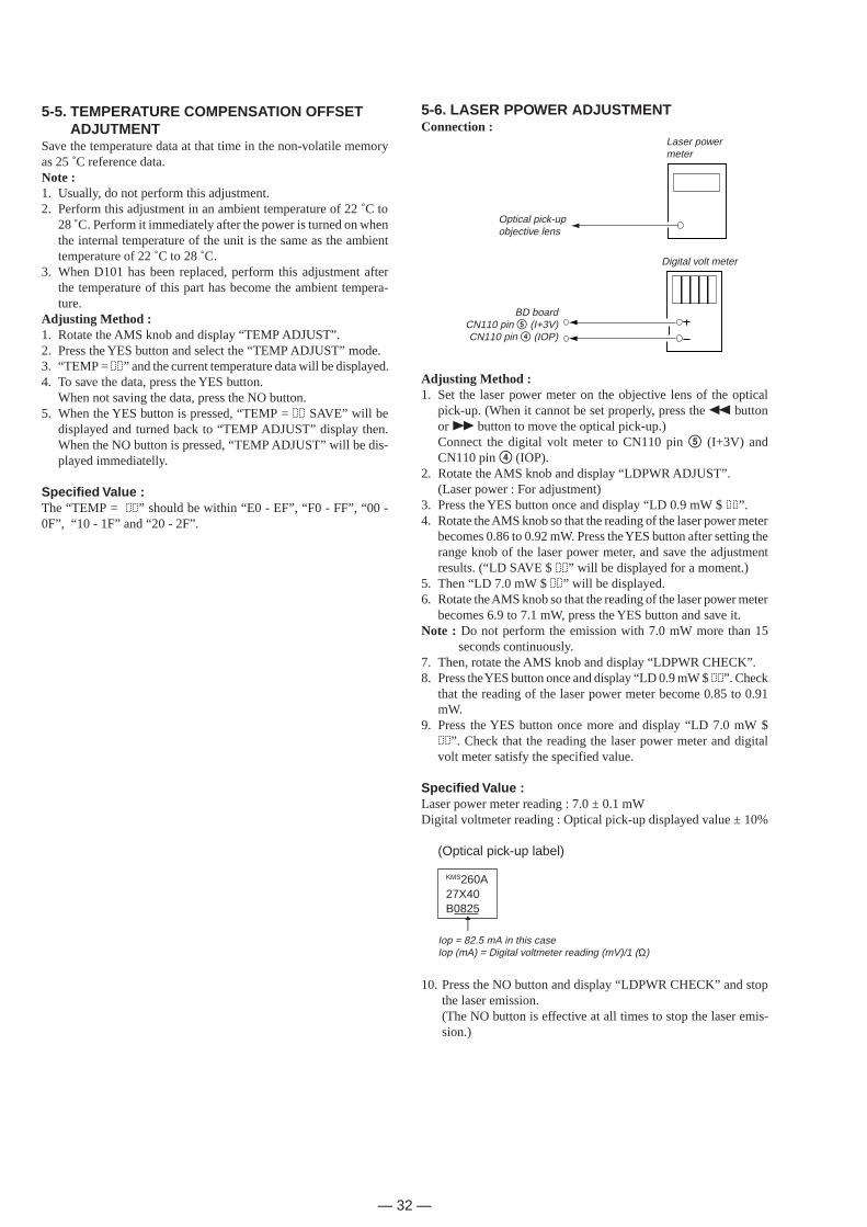
5-6. LASER PPOWER ADJUSTMENTConnection :
Laser powermeter
Optical pick-upobjective lens
Digital volt meter
BD boardCN110 pin 5 (I+3V)CN110 pin 4 (IOP)
Adjusting Method :1. Set the laser power meter on the objective lens of the optical
pick-up. (When it cannot be set properly, press the 0 buttonor ) button to move the optical pick-up.)Connect the digital volt meter to CN110 pin 5 (I+3V) andCN110 pin 4 (IOP).
2. Rotate the AMS knob and display “LDPWR ADJUST”.(Laser power : For adjustment)
3. Press the YES button once and display “LD 0.9 mW $ ”.4. Rotate the AMS knob so that the reading of the laser power meter
becomes 0.86 to 0.92 mW. Press the YES button after setting therange knob of the laser power meter, and save the adjustmentresults. (“LD SAVE $ ” will be displayed for a moment.)
5. Then “LD 7.0 mW $ ” will be displayed.6. Rotate the AMS knob so that the reading of the laser power meter
becomes 6.9 to 7.1 mW, press the YES button and save it.Note : Do not perform the emission with 7.0 mW more than 15
seconds continuously.7. Then, rotate the AMS knob and display “LDPWR CHECK”.8. Press the YES button once and display “LD 0.9 mW $ ”. Check
that the reading of the laser power meter become 0.85 to 0.91mW.
9. Press the YES button once more and display “LD 7.0 mW $”. Check that the reading the laser power meter and digital
volt meter satisfy the specified value.
Specified Value :Laser power meter reading : 7.0 ± 0.1 mWDigital voltmeter reading : Optical pick-up displayed value ± 10%
(Optical pick-up label)
KMS260A27X40B0825N
Iop = 82.5 mA in this caseIop (mA) = Digital voltmeter reading (mV)/1 (Ω)
10. Press the NO button and display “LDPWR CHECK” and stopthe laser emission.(The NO button is effective at all times to stop the laser emis-sion.)
— 33 —
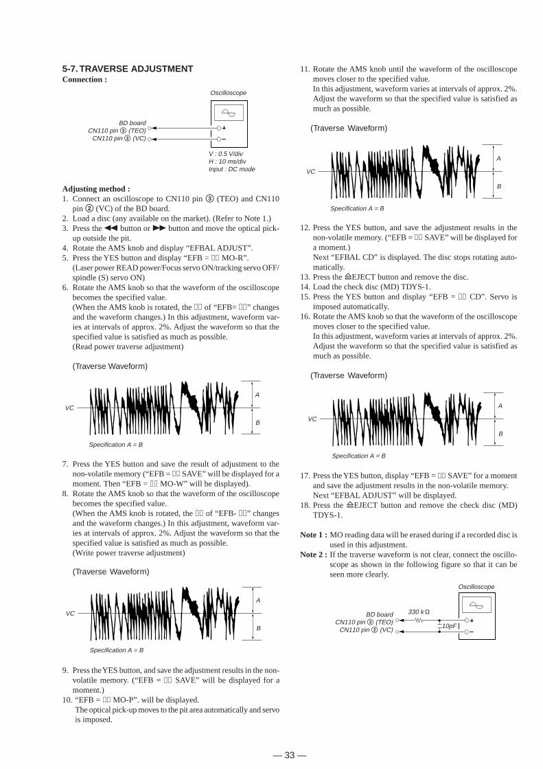
5-7. TRAVERSE ADJUSTMENTConnection :
Oscilloscope
V : 0.5 V/divH : 10 ms/divInput : DC mode
BD boardCN110 pin 3 (TEO)
CN110 pin 2 (VC)
Adjusting method :1. Connect an oscilloscope to CN110 pin 3 (TEO) and CN110
pin 2 (VC) of the BD board.2. Load a disc (any available on the market). (Refer to Note 1.)3. Press the 0 button or ) button and move the optical pick-
up outside the pit.4. Rotate the AMS knob and display “EFBAL ADJUST”.5. Press the YES button and display “EFB = MO-R”.
(Laser power READ power/Focus servo ON/tracking servo OFF/spindle (S) servo ON)
6. Rotate the AMS knob so that the waveform of the oscilloscopebecomes the specified value.(When the AMS knob is rotated, the of “EFB= ” changesand the waveform changes.) In this adjustment, waveform var-ies at intervals of approx. 2%. Adjust the waveform so that thespecified value is satisfied as much as possible.(Read power traverse adjustment)
(Traverse Waveform)
VC
A
B
Specification A = B
7. Press the YES button and save the result of adjustment to thenon-volatile memory (“EFB = SAVE” will be displayed for amoment. Then “EFB = MO-W” will be displayed).
8. Rotate the AMS knob so that the waveform of the oscilloscopebecomes the specified value.(When the AMS knob is rotated, the of “EFB- ” changesand the waveform changes.) In this adjustment, waveform var-ies at intervals of approx. 2%. Adjust the waveform so that thespecified value is satisfied as much as possible.(Write power traverse adjustment)
(Traverse Waveform)
VC
A
Specification A = B
B
9. Press the YES button, and save the adjustment results in the non-volatile memory. (“EFB = SAVE” will be displayed for amoment.)
10. “EFB = MO-P”. will be displayed.The optical pick-up moves to the pit area automatically and servois imposed.
11. Rotate the AMS knob until the waveform of the oscilloscopemoves closer to the specified value.In this adjustment, waveform varies at intervals of approx. 2%.Adjust the waveform so that the specified value is satisfied asmuch as possible.
(Traverse Waveform)
VC
A
B
Specification A = B
12. Press the YES button, and save the adjustment results in thenon-volatile memory. (“EFB = SAVE” will be displayed fora moment.)Next “EFBAL CD” is displayed. The disc stops rotating auto-matically.
13. Press the §EJECT button and remove the disc.14. Load the check disc (MD) TDYS-1.15. Press the YES button and display “EFB = CD”. Servo is
imposed automatically.16. Rotate the AMS knob so that the waveform of the oscilloscope
moves closer to the specified value.In this adjustment, waveform varies at intervals of approx. 2%.Adjust the waveform so that the specified value is satisfied asmuch as possible.
(Traverse Waveform)
VC
A
B
Specification A = B
17. Press the YES button, display “EFB = SAVE” for a momentand save the adjustment results in the non-volatile memory.Next “EFBAL ADJUST” will be displayed.
18. Press the §EJECT button and remove the check disc (MD)TDYS-1.
Note 1 :MO reading data will be erased during if a recorded disc isused in this adjustment.
Note 2 : If the traverse waveform is not clear, connect the oscillo-scope as shown in the following figure so that it can beseen more clearly.
Oscilloscope
330 k Ω
10pF
BD boardCN110 pin 3 (TEO)
CN110 pin 2 (VC)
— 34 —
5-8. FOCUS BIAS ADJUSTMENTAdjusting Method :1. Load a continuously recorded disc (Refer to “5-4. Creating Con-
tinuously Recorded Disc”.).2. Rotate the AMS knob and display “CPLAY MODE”.3. Press the YES button and display “CPLAY MID”.4. Press the NO button when “C1 = AD = ” is displayed.5. Rotate the AMS knob and display “FBIAS ADJUST”.6. Press the YES button and display “ / a = ”.
The first four digits indicate the C1 error rate, the two digitsafter [/] indicate ADER, and the 2 digits after [a =] indicate thefocus bias value.
7. Rotate the AMS knob in the clockwise direction and find thefocus bias value at which the C1 error rate becomes 220 (Referto Note 2).
8. Press the YES button and display “ / b = ”.9. Rotate the AMS knob in the counterclockwise direction and find
the focus bias value at which the C1 error rate becomes 220.10. Press the YES button and display “ / c = ”.11. Check that the C1 error rate is below 50 and ADER is 00. Then
press the YES button.12. If the “( )” in “ - - ( )” is above 20, press the YES
button.If below 20, press the NO button and repeat the adjustment fromstep 2.
13. Press the §EJECT button to remove the continuously recordeddisc.
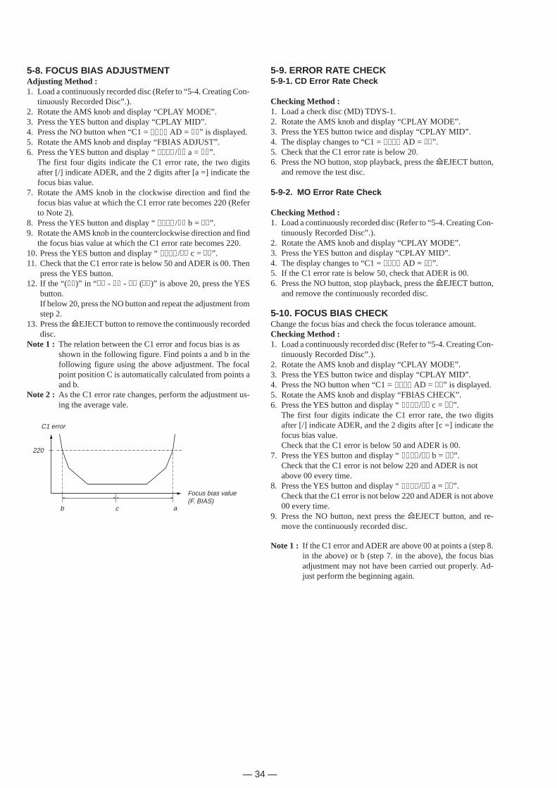
Note 1 : The relation between the C1 error and focus bias is asshown in the following figure. Find points a and b in thefollowing figure using the above adjustment. The focalpoint position C is automatically calculated from points aand b.
Note 2 : As the C1 error rate changes, perform the adjustment us-ing the average vale.
220
C1 error
b c a
Focus bias value(F. BIAS)
5-9. ERROR RATE CHECK5-9-1. CD Error Rate Check
Checking Method :1. Load a check disc (MD) TDYS-1.2. Rotate the AMS knob and display “CPLAY MODE”.3. Press the YES button twice and display “CPLAY MID”.4. The display changes to “C1 = AD = ”.5. Check that the C1 error rate is below 20.6. Press the NO button, stop playback, press the §EJECT button,
and remove the test disc.
5-9-2. MO Error Rate Check
Checking Method :1. Load a continuously recorded disc (Refer to “5-4. Creating Con-
tinuously Recorded Disc”.).2. Rotate the AMS knob and display “CPLAY MODE”.3. Press the YES button and display “CPLAY MID”.4. The display changes to “C1 = AD = ”.5. If the C1 error rate is below 50, check that ADER is 00.6. Press the NO button, stop playback, press the §EJECT button,
and remove the continuously recorded disc.
5-10. FOCUS BIAS CHECKChange the focus bias and check the focus tolerance amount.Checking Method :1. Load a continuously recorded disc (Refer to “5-4. Creating Con-
tinuously Recorded Disc”.).2. Rotate the AMS knob and display “CPLAY MODE”.3. Press the YES button twice and display “CPLAY MID”.4. Press the NO button when “C1 = AD = ” is displayed.5. Rotate the AMS knob and display “FBIAS CHECK”.6. Press the YES button and display “ / c = ”.
The first four digits indicate the C1 error rate, the two digitsafter [/] indicate ADER, and the 2 digits after [c =] indicate thefocus bias value.Check that the C1 error is below 50 and ADER is 00.
7. Press the YES button and display “ / b = ”.Check that the C1 error is not below 220 and ADER is notabove 00 every time.
8. Press the YES button and display “ / a = ”.Check that the C1 error is not below 220 and ADER is not above00 every time.
9. Press the NO button, next press the §EJECT button, and re-move the continuously recorded disc.
Note 1 : If the C1 error and ADER are above 00 at points a (step 8.in the above) or b (step 7. in the above), the focus biasadjustment may not have been carried out properly. Ad-just perform the beginning again.
— 35 —
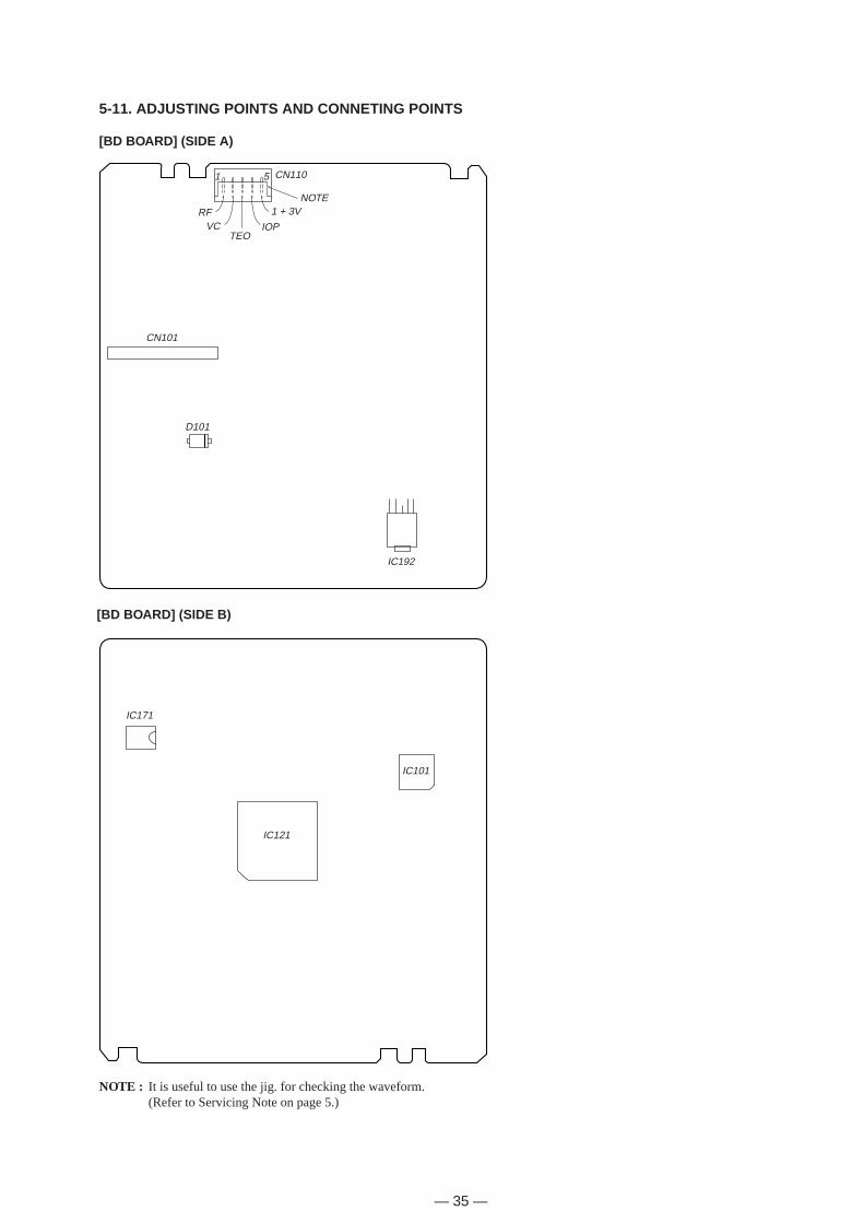
5-11. ADJUSTING POINTS AND CONNETING POINTS
[BD BOARD] (SIDE A)
IC192
NOTE : It is useful to use the jig. for checking the waveform.(Refer to Servicing Note on page 5.)
[BD BOARD] (SIDE B)
1 5 CN110
RFVC
TEOIOP
1 + 3VNOTE
CN101
D101
IC171
IC101
IC121
— 36 —
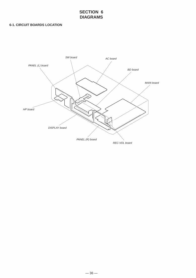
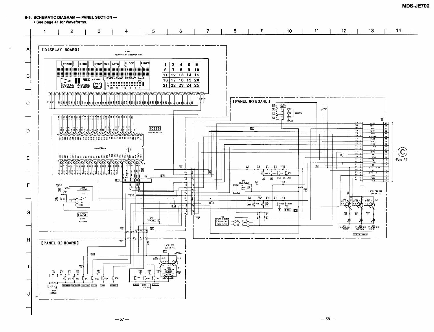
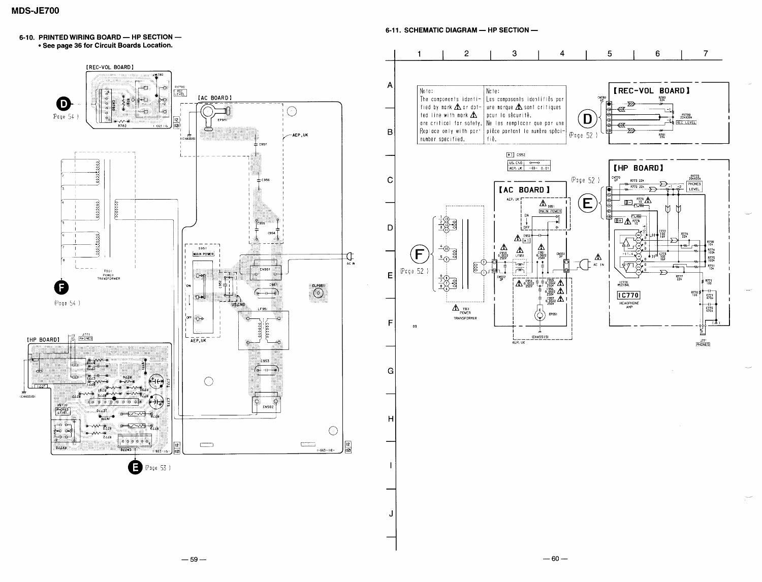
SECTION 6DIAGRAMS
6-1. CIRCUIT BOARDS LOCATION
AC boardSW board
PANEL (L) board
HP board
DISPLAY board
PANEL (R) boardREC-VOL board
MAIN board
BD board
HR901OVER WRITE
HEADHEADDRIVE
Q181,182
11
14
15
17
3
918 2
118 Q180
FILT
ER
PCOFILIFILOCLTV
PLL
EFM,ACIRC,
ENCODER/DECODER
RF AGC & EQ
AGCI
RFO
MOR
FIM
ORFO
RF AMP12
BPF P-P
ATAMP BPF
VCVC
ANALOGMUX
27
161718
SERIAL
PARALLELDECODER
VICONV
20
2522 23
456789
IV AMP
IV AMP
E-FBALANCE
14
15
3
VCCVC
D101
1211
10LASER ON
SWQ101
PD
APCQ162,163
HFMODULE
HF MODULESW
IC103,Q102-104
TRAKINGCOIL
FOCUSCOIL 10
12DRIVER
21DRIVER
23
27DRIVER
25
68
DRIVER
16
TFDR
PSBXRST
SLED/SPINDLE MOTOR DRIVEFOCUS/TRACKING COIL DRIVE
IC152
09
M
M
M902SLED MOTOR
M901SPINDLE MOTOR
DETECTOR
F
I JCD
BA
E
VC
LD
PD
ILCC
15 14
SHOCKRESISTANTMEMORY
CONTROLLER
ATRACENCODER/DECODER
SAMPLINGRATE
CONVERTER
DTRFCKRFXLRF
FOCNT79
828180
93 94
SPRD
SPFD
SPINDLESERVO
ADIPDEMODULATOR/
DECODER78
ADFG
A/DCONVERTER
APCSERVO
DSP
PWMGENERATOR
10
DIGITALAUDIO
I/F
22
24
23
21
SUBCODEPROCESSOR
1112
MONITOR
CONTROL
4321
3
CPUI/F
AUTOSEQUENCER
16
2526
75689
1 5 512FS
MM903LOADING MOTOR
BCKLRCK
BUFFERIC123
SQSYDQSY
MNT3MNT2MNT1MNT0
SENSSRDTSCLKSWDTXLAT
DIN
ADDT
DADT
DOUT
XRST
9192858689888313
RECP
APCR
EFFF
DRFR
DRTF
DRTR
DRSF
DRSR
DR
FOCNT
XLATSCLK
SWDT
CSLED
SE
TE2628
32
30
ADFG
ADIN
ADFM29
31
34 6567
7473
EEVC
TESE
33 66
3637
35
6362
64
AUX
BOTMPEAK
ABCD
FE
AUX1
BOTMPEAK
ABCD
38RF
55RFI
58596061
ABCDAMP
FOCUSERROR
AMP
IJ
ABCD
EF
VC CVB
TEMPAMP
TEMPR
TEMPI
APC
APCR
EF
EQAD
J3T
ADJ
WBL
ADJ
TRACKINGERROR
AMP
OPTICAL PICK-UP BLOCK(KMS-260A/J1N)
48 47 46 40
RF AMPIC101
EFMO
TX XINI
T
CLOCKGENERATOR
8586
8988
9291
9493
SPFDSPRD
SFDRSRDR
TRDR
FRDRFFDR
OVER WRITE HEAD DRIVEIC181
OSCI
XBCKLRCK
VC
VC
PEAK&
BOTTOM
TRK–TRK+
FSC+FSC–
SLED+SLED–
SPDL+SPDL–
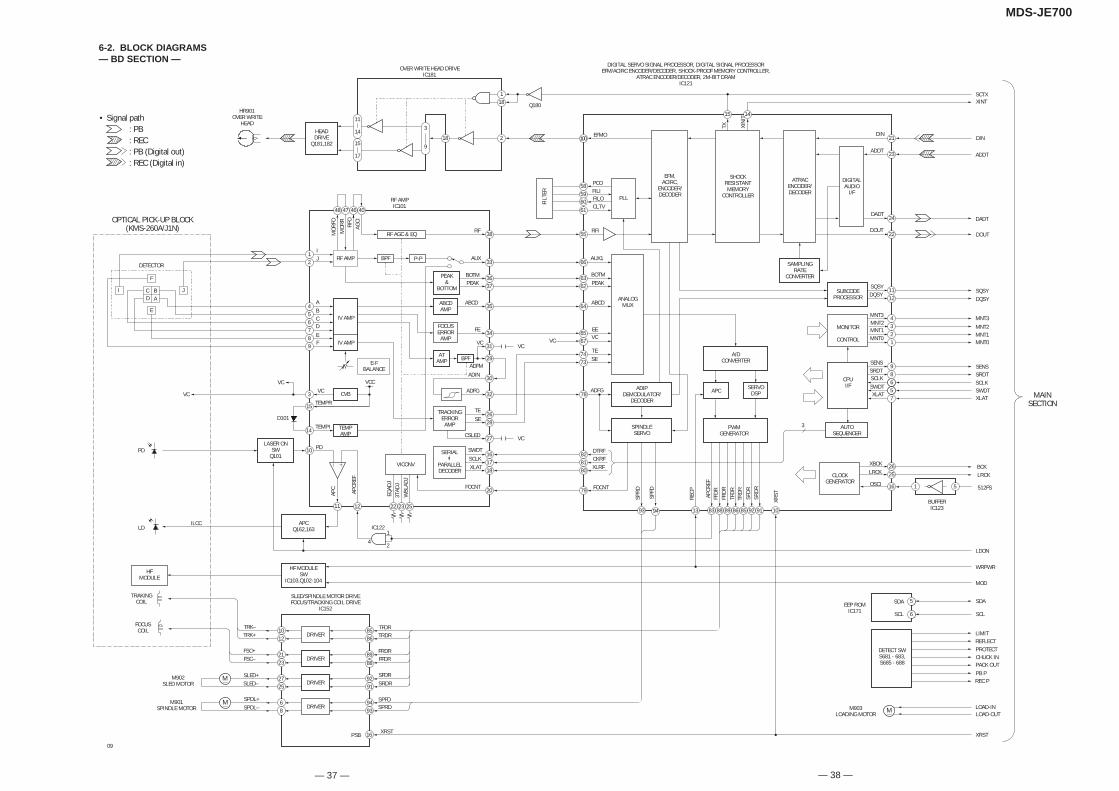
DIGITAL SERVO SIGNAL PROCESSOR, DIGITAL SIGNAL PROCESSOREFM/ACIRC ENCODER/DECODER, SHOCK-PROOF MEMORY CONTROLLER,
ATRAC ENCODER/DECODER, 2M-BIT DRAMIC121
IC122
42
1
SCTXXINT
DIN
ADDT
DADT
DOUT
SQSYDQSY
MNT3MNT2MNT1MNT0
SENSSRDTSCLKSWDTXLAT
LDON
WRPWR
MOD
6
5 SDASDA
SCLSCL
LIMITREFLECTPROTECTCHUCK INPACK OUTPB PREC P
EEP ROMIC171
LOAD-INLOAD-OUT
XRST
MAINSECTION
DETECT SWS681 - 683,S685 - 688
100
• Signal path : PB : REC : PB (Digital out) : REC (Digital in)
— 37 — — 38 —
MDS-JE700
6-2. BLOCK DIAGRAMS— BD SECTION —
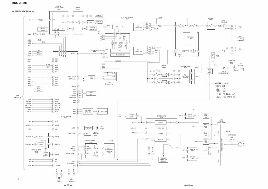
— MAIN SECTION —
— 39 — — 40 —
MDS-JE700
16
15
1
DIGITALOPTICAL OUT
IC352
SQSY
DQSY
12
5
610
2
4
LOAD-IN
LOADING MOTORDRIVEIC351
DRIVE
DRIVE
LOADINGSW
Q351,352
DIG-RST
XOUT
81
27 28
X40212MHz
25 24
X40132.768KHz
SCLKSWDTXLAT
SYSTEM CONTROLIC401
SWDT
27
18
DADT
INIT
I/O
25 28 26
10 11
CPU INTERFACE
19 20 21
22
D/ACONVERTER
R-ch
1716
+ L1– L2+ R1
– R2
41393032
15
A/DCONVERTER
555612
I/O
A/D, D/A CONVERTERIC304
12
15
4
345 MATRIX
SW
14
13
2320
DISPLAY DRIVERIC730
FL730FLUORESCENT
INDICATORTUBE
AC
LPF 1
MUTE
FRONT-ENDIC302
MUTESW
Q301
R-ch
MUTEQ101
HEADPHONEAMPIC770
RV770PHONES LEVEL
R-ch
R-ch
J301LINE
(ANALOG)
IN
OUT
57
6BACK UP
4+5V REG
+3.3V REG
+5V REG
5
1
15 +3V REGIC192
+3V(BD)
PH +5V
SYS +3.3V
ANA +5V
3
SWITCHING REGIC901
7
8212 9
POWERON/OFF SWQ350, 402
S. R
ESET
P. D
OWN
31 +6V REGIC903+6V
+BRECTD903,904
RECTD901,902
RECTD907,908
–B
23 –6V REGIC904–6V
13 –32V REGIC902–32V
AC
AC
FL730
ACIN
T901POWER
TRANSFORMAER
R-ch
PHONES
J771
2324
R-ch
INLMINLPINRPINRM
ADDT
X30122MHz
35 36
XIN
XOUT
256C
K
SCLKXLAT
83DA-RST
93
4617
AMUTE
D351
CNTRL A1 OUTCNTRL A1 IN
KEY0KEY1KEY2
5051
JOG1JOG0
43LED0 LED DRIVEQ750,751 POWER
D750
3 RMSIRCS
RECEIVERIC731
REMOCOM
717273
626361
60
4
39
40
55
FLCLKFLDATA
FLCS
POWER DOWN
SCKSDATACS
RST
S1
S36
D1
D16
36
VBATSYSTEM-RST
STB
XOUT
-T
XIN-
T
XIN
39 LOAD V
94 LOAD OUT
86 MOD
LOAD IN95
75
80
LDON
WRPWR
3269676890
42
4133
77
MNT3
MNT2SHOCK
FOK
89
XINT
SCTX
SQSYDQSY
MNT3MNT2MNT1
MNT0
DOUT
MCK
1
BCKLRCK512FS
SLOCK
XBUSY
52 SDA53 SCL
LOAD-OUT
SDASCL
XRST
MOD
WRPWR
LDON
9698
9768
LIMITINREFLECTPROTECT
CHUCK INPACK OUT
3837
PLAY P
REC P
LIMITREFLECTPROTECT
CHUCK INPACK-OUT
PB-P
REC-P
SENSSRDTSCLK
SWDT
XLAT
SENSSRDTSCLKSWDTXLATCH
BCKLRCK512FS
BCKLRCK512FS
ADDTDADTSCTXXINT
6
4
DIN
2
7
5
14
DIGITALDATA SELECTOR
IC356
IC0
IC1
IC2
1Y
A A B B
84 85
DSEL
ADS
EL B
12
10
9
IC353
IC354
13
11
3
3
DIGITALCOAXIAL IN
J352
910
TIMER SWSOURCE SW
5455
FS32FS44 D701 - 703
16 DPD
1
13
9
11
12 3
2
4
8
610 5
BUFFERIC101
22
23
26
25
36
35
ECLSWITCHING
CIRCUITLPF
26 25
14
REC LEVELRV780
5 7
RECTD905,906
BDSECTION
• R CH is omitted.• Signal path : PB : REC : PB (Digital out) : REC (Digital in)
09
+B
8
BUFFERIC355
CURRENT PULSEIC303 IC102
LINE AMPIC301
56FS48
LED DRIVEQ701 - 703
DIGITALOPTICAL IN1
AMPQ353
J350CONTROL A1
R
R
L
L
S951
MAIN POWER
AEP, UK
DIGITALOPTICAL IN2
— 61 —
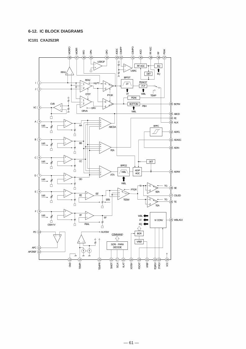
6-12. IC BLOCK DIAGRAMS
IC101 CXA2523R
–1
–2
+–IVR BB
+–IVR AA
+–IVR CC
+–IVR DD
+–IVR
+–
EE EE'
EFB TESW
PTGR
48
MOR
FO
47
MOR
FI
46
RFO
45
OPN
44
OPO
43
ADDC
42
COM
PP
41
COM
PO
40
AGCI
39
RF A
GC
38
RF
37
PEAK
36 BOTM
35 ABCD
34 FE
33 AUX
32 ADFG
31 ADAGC
30 ADIN
29 ADFM
28 SE
27 CSLED
26 TE
25 WBLADJ
24
VCC
23
3TAD
J
22
EQAD
J
21
VREF
20
F0CN
T
19
XSTB
Y
18
XLAT
17
SCLK
16
SWDT
15
TEM
PR
14
TEM
PI
13
GND
12APCREF
11APC
10PD
9F
8E
7D
6C
5B
4A
3VC
VI CONV
BGR
VREFSCRI - PARA
DECODE
+ –
+–
AUXSWCOMMAND
+–IVR
GSW IV
+–
FF
FBAL
FF'
TG
SEA–+–+
–1
–2
TG
TEA
WBL
3T
EQ
––++
++––
++++
DET
ADIPAGCWBL
BPF22
BPFCABCDA
FEA
WBL
ATA
–+CVB
+ –RFA1
––––
1
2
–––
12
GRVA
CFST
RFA2
GRV
HLPT
PTGR
–2
–1
–1
–2
BOTTOM
PEAK
RF AGC EQ
EQDET
P-P
WBL
3T WBLTEMP
PBH
–+
USROP
+– USRC
3T
BPF3T
PEAK3T1I
2J
— 62 —
100 99 98 97 96 95 94 93
EFM
O
DVSS
TEST
3
TEST
2
TEST
1
TEST
0
SPFD
SPRD
92
SFDR
91
SRDR
90
FS4
89
KRDR
88
FFDR
87
DVDD
86
TFDR
85
TRDR
84
LDDR
83
APCR
EF
82
DTRF
81
CKRF
80
XLRF
79
F0CN
T
78
ADFG
77
APC
76
DCHG
75 AUX2
74 TE
73 SE
72 AVSS
71 ADRB
70 ADRT
69 AVDD
68 ADIO
61 CLTV
60 FILO
59 FILI
58 PCO
57 PDO
55 RFI
56 AVSS
54 BIAS
53 AVDD
52 ASYI
51 ASYO
67 VC
66 AUX1
65 FE
64 ABCD
63 BOTM
62 PEAK
50
MVC
I
49
D3
48
D2
47
D0
46
D1
45
XWE
44
XRAS
43
A09
42
XCAS
41
XOE
40
DVSS
39
A11
38
A08
37
A07
36
A06
35
A05
34
A04
33
A10
32
A00
31
A01
30
A02
29
A03
28
DVDD
26
XBCK
27
FS25
6
25LRCK
24DADT
23ADDT
22DOUT
21DIN
20RVSS
19RVDD
18XTSL
17OSCO
16OSCI
15TX
14XINT
13RECP
12DQSY
11SQSY
10XRST
9SENS
8SRDT
7XLAT
6SCLK
5SWDT
4MNT3
3MNT2
2MNT1
1MNT0
PWMGENERATOR
AUTO
SEQU
ENCE
R
SERVODSP
CPU I/F
MONITORCONTROL
SPINDLESERVO
EACHBLOCK
EACHBLOCK
DIGITALAUDIO
I/F
SAMPLINGRATE
CONVERTER
CLOCKGENERATOR
SUBCODEPROCESSOR
EACHBLOCK
A/DCONVERTER
ANALOGMUX
EFM
/ACI
RCEN
CODE
R/DE
CODE
R
APC
PLL
SHOCK RESISTANTMEMORY CONTROLLER
ATRACENCODER/DECODER
DRAM
ADIPDEMODULATOR/
DECODER
COMP
ADDRESS/DATA BUS A00 - A11, D0 - D3
IC121 CXD2650R
— 63 —
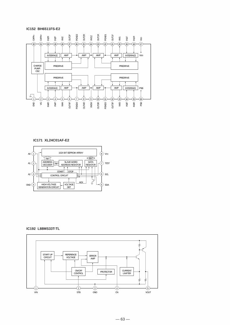
IC152 BH6511FS-E2
32 31 30 29 28 27 26 25 24 23 22 21 20 19 18 17
1 2 3 4 5 6 7 8 9 10 11 12 13 14 15 16
GND VG
IN4R
IN4F
VM4
OUT4
F
PGND
4
OUT4
R
VM34
OUT3
R
PGND
3
OUT3
F
VM3
IN3F
IN3R PS
B
CAPA
–
CAPA
+
IN2R
IN2F
VM2
OUT2
F
PGND
2
OUT2
R
VM12
OUT1
R
PGND
1
OUT1
F
VM1
IN1F
IN1R
V DD
CHARGEPUMP.
OSC
INTERFACE AMP
INTERFACE AMP
AMP INTERFACE
PREDRIVEPREDRIVE
PREDRIVEPREDRIVE
AMP
INTERFACEAMPAMPAMP
VDD
PSB
AMP
ADDRESSDECODER
HIGH VOLTAGEGENERATION CIRCUIT
VOLTAGEDET
7BIT
7BIT
8BIT
DATARESISTOR
SLAVE WORDADDRESS RESISTOR
CONTROL CIRCUIT
START STOP
ACK
1024 BIT EEPROM ARRAYA0
A1
A2
GND
VCC
TEST
SCL
SDA
1
3
2
4
8
6
7
5
IC171 XL24C01AF-E2
IC192 L88MS33T-TL
1 2 3 4 5
START UPCIRCUIT
REFERENCEVOLTAGE
ERRORAMP
VIN STB GND CN VOUT
ON/OFFCONTROL
CURRENTLIMITER
PROTECTOR
— 64 —
–+
1
2
3
4
5
6
7
8
9
31
30
29
28
27
26
25
24
23
13.2k
2.35k
2.35k
13.2k13.2k
VCC
10
11
12
13
22
21
20
19
36
35
34
33
32
16
17
18
14
15
–+
–+
–+
–+
+–
–+
–+
+–
+–
VEE
LINE02
PMUTE
LINE01
MUTE
LINE/MIC
+D/A1
+D/A1
+D/AO1
LP1N1
LPOUT1
GND1
LPOUT2
LPIN2
D/AO2
–D/A2
+D/A2
VCC
VDD
–+
LINE1
VEE
MIC1
SW01
SWI1
–A/D1
INV1
+A/D1
A/DREF
VREF
+A/D2
INV2
–A/D2
SWI2
SWO2
MIC2
GND2
LINE2
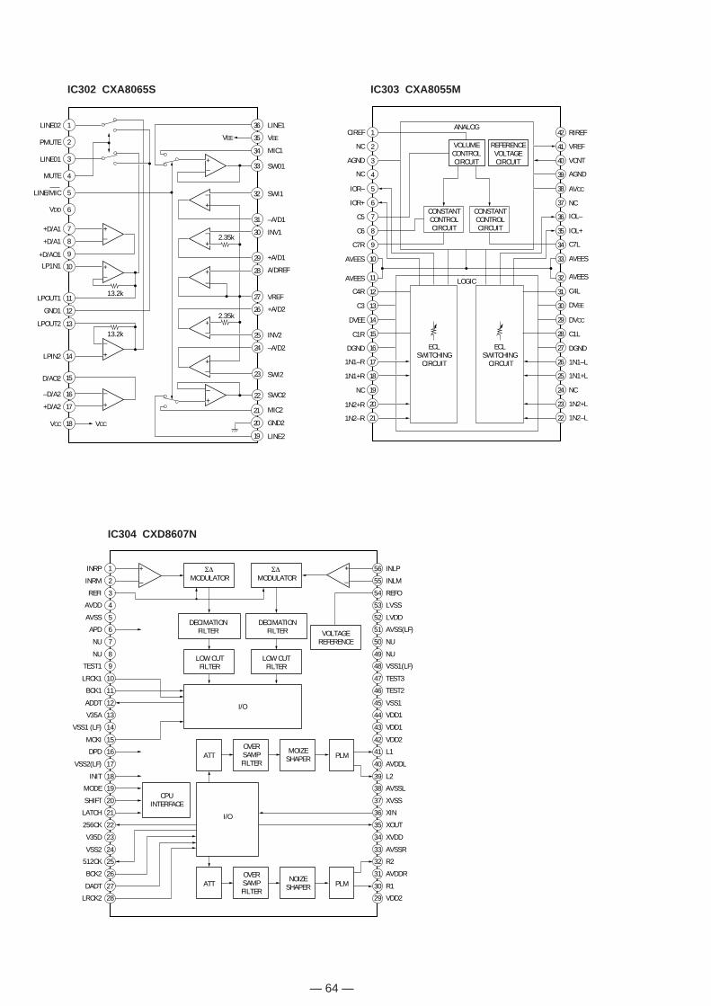
IC302 CXA8065S
42
41
40
39
38
37
36
35
34
33
31
30
29
28
27
26
25
24
23
22
32
1CIREFANALOG
VOLUMECONTROLCIRCUIT
CONSTANTCONTROLCIRCUIT
ECLSWITCHING
CIRCUIT
ECLSWITCHING
CIRCUIT
LOGIC
REFERENCEVOLTAGECIRCUIT
NC
AGND
NC
IOR–
IOR+
C5
C6
C7R
AVEES
AVEES
C4R
C3
DVEE
C1R
DGND
1N1–R
1N1+R
NC
1N2+R
1N2–R
RIREF
VREF
VCNT
AGND
AVCC
NC
IOL–
IOL+
C7L
AVEES
AVEES
C4L
DVEE
DVCC
C1L
DGND
1N1–L
1N1+L
NC
1N2+L
1N2–L
2
3
4
5
6
7
8
9
10
12
13
14
15
16
17
18
19
20
21
11
CONSTANTCONTROLCIRCUIT
IC303 CXA8055M
1
2
3
4
5
6
7
8
9
10
11
12
13
14
15
16
17
18
19
20
21
22
23
24
25
26
27
28
INRP
INRM
REFI
AVDD
AVSS
APD
NU
NU
TEST1
LRCK1
BCK1
ADDT
V35A
VSS1 (LF)
MCKI
DPD
VSS2(LF)
INIT
MODE
SHIFT
LATCH
256CK
V35D
VSS2
512CK
BCK2
DADT
LRCK2
56
55
54
53
52
51
50
49
48
47
46
45
44
43
42
41
40
39
38
37
36
35
34
33
32
31
30
29
INLP
INLM
REFO
LVSS
LVDD
AVSS(LF)
NU
NU
VSS1(LF)
TEST3
TEST2
VSS1
VDD1
VDD1
VDD2
L1
AVDDL
L2
AVSSL
XVSS
XIN
XOUT
XVDD
AVSSR
R2
AVDDR
R1
VDD2
MODULATOR MODULATOR
DECIMATIONFILTER
DECIMATIONFILTER
LOW CUTFILTER
LOW CUTFILTER
VOLTAGEREFERENCE
I/O
I/O
ATT PLMOVERSAMPFILTER
MOIZESHAPER
CPUINTERFACE
+
–
+
–
ATT PLMOVERSAMPFILTER
NOIZESHAPER
IC304 CXD8607N
— 65 —
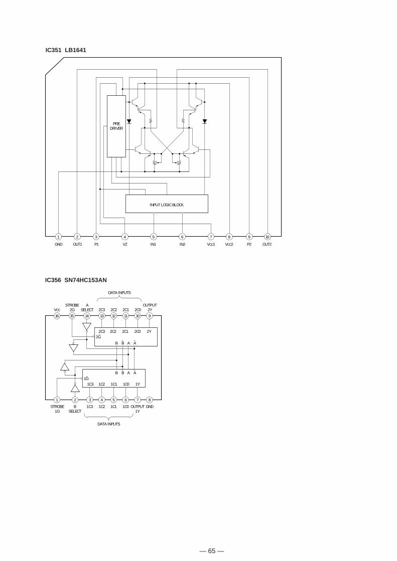
IC351 LB1641
109876543
PREDRIVER
INPUT LOGIC BLOCK
GND OUT1 P1 VZ IN1 IN2 VCC1 VCC2 P2 OUT2
21
IC356 SN74HC153AN
16
1 2 3 4 5 6 7 8
15 14 13 12
2C3 2C2
B AB A
2C1 2C0 2Y
1C3 1C2 1C1 1C0 1Y
VCC 2C3 2C2 2C1 2C0
DATA INPUTS
DATA INPUTS
STROBE2G
STROBE1G
BSELECT
1C3 1C2 1C1 1C0 OUTPUT1Y
GND
ASELECT
OUTPUT2Y
2G
11 10 9
1GB AB A
— 66 —
1–+
12
DELAYCIRCUIT
VREF
DELAYCIRCUIT
3.3V
PH5
STBY
VCC
ANA5
SYS3.3
BACK
AC
CD1
P. DOWN
GND
CD2
S. RESET
–+
–+
–+
–+
–+
2
3
4
5
6
7
8
9
10
11
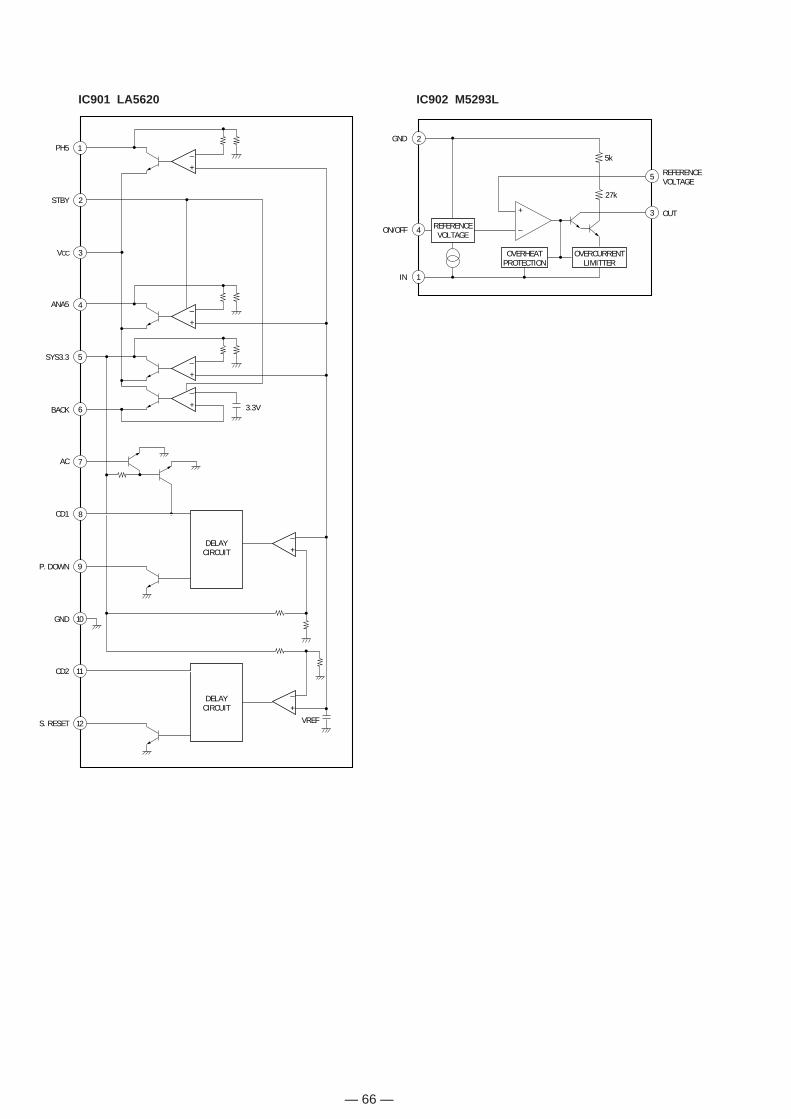
IC901 LA5620
2
5
5k
+
–
27k
OVERCURRENTLIMITTER
OVERHEATPROTECTION
REFERENCEVOLTAGE
GND
ON/OFF
IN
REFERENCEVOLTAGE
OUT3
4
1
IC902 M5293L
— 67 —
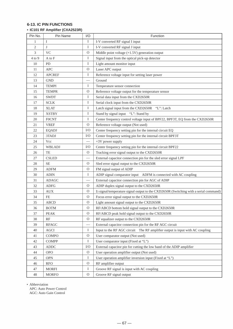
6-13. IC PIN FUNCTIONS• IC101 RF Amplifier (CXA2523R)
Pin No. Pin Name I/O Function
1
2
3
4 to 9
10
11
12
13
14
15
16
17
18
19
20
21
22
23
24
25
26
27
28
29
30
31
32
33
34
35
36
37
38
39
40
41
42
43
44
45
46
47
48
I
J
VC
A to F
PD
APC
APCREF
GND
TEMPI
TEMPR
SWDT
SCLK
XLAT
XSTBY
F0CNT
VREF
EQADJ
3TADJ
Vcc
WBLADJ
TE
CSLED
SE
ADFM
ADIN
ADAGC
ADFG
AUX
FE
ABCD
BOTM
PEAK
RF
RFAGC
AGCI
COMPO
COMPP
ADDC
OPO
OPN
RFO
MORFI
MORFO
I
I
O
I
I
O
I
—
I
O
I
I
I
I
I
O
I/O
I/O
—
I/O
O
—
O
O
I
—
O
O
O
O
O
O
O
—
I
O
I
I/O
O
I
O
I
O
I-V converted RF signal I input
I-V converted RF signal J input
Middle point voltage (+1.5V) generation output
Signal input from the optical pick-up detector
Light amount monitor input
Laser APC output
Reference voltage input for setting laser power
Ground
Temperature sensor connection
Reference voltage output for the temperature sensor
Serial data input from the CXD2650R
Serial clock input from the CXD2650R
Latch signal input from the CXD2650R “L”: Latch
Stand by signal input “L”: Stand by
Center frequency control voltage input of BPF22, BPF3T, EQ from the CXD2650R
Reference voltage output (Not used)
Center frequency setting pin for the internal circuit EQ
Center frequency setting pin for the internal circuit BPF3T
+3V power supply
Center frequency setting pin for the internal circuit BPF22
Tracking error signal output to the CXD2650R
External capacitor connection pin for the sled error signal LPF
Sled error signal output to the CXD2650R
FM signal output of ADIP
ADIP signal comparator input ADFM is connected with AC coupling
External capacitor connection pin for AGC of ADIP
ADIP duplex signal output to the CXD2650R
I3 signal/temperature signal output to the CXD2650R (Switching with a serial command)
Focus error signal output to the CXD2650R
Light amount signal output to the CXD2650R
RF/ABCD bottom hold signal output to the CXD2650R
RF/ABCD peak hold signal output to the CXD2650R
RF equalizer output to the CXD2650R
External capacitor connection pin for the RF AGC circuit
Input to the RF AGC circuit The RF amplifier output is input with AC coupling
User comparator output (Not used)
User comparator input (Fixed at “L”)
External capacitor pin for cutting the low band of the ADIP amplifier
User operation amplifier output (Not used)
User operation amplifier inversion input (Fixed at “L”)
RF amplifier output
Groove RF signal is input with AC coupling
Groove RF signal output
• AbbreviationAPC: Auto Power ControlAGC: Auto Gain Control
— 68 —
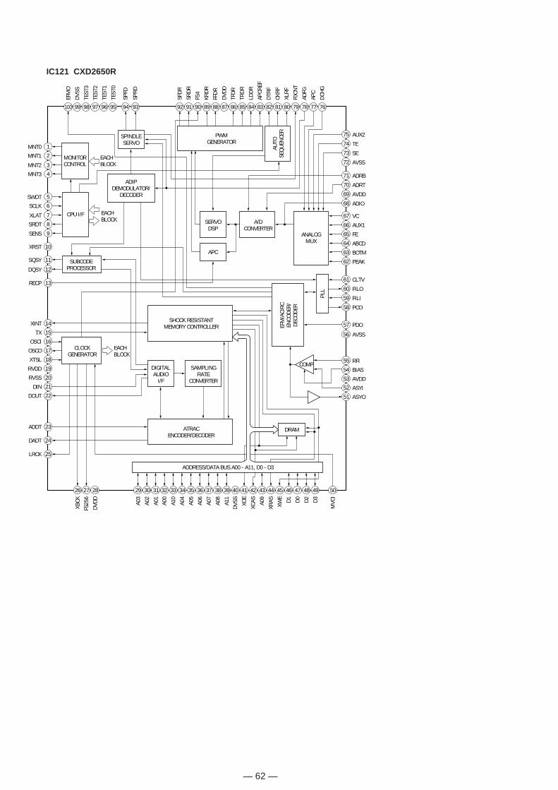
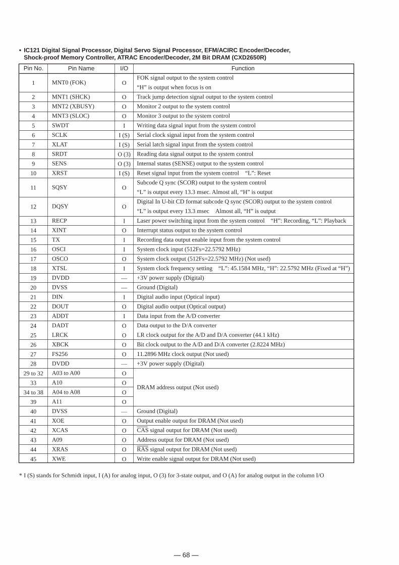
• IC121 Digital Signal Processor, Digital Servo Signal Processor, EFM/ACIRC Encoder/Decoder,Shock-proof Memory Controller, ATRAC Encoder/Decoder, 2M Bit DRAM (CXD2650R)
FunctionPin No. Pin Name I/O
1
2
3
4
5
6
7
8
9
10
11
12
13
14
15
16
17
18
19
20
21
22
23
24
25
26
27
28
29 to 32
33
34 to 38
39
40
41
42
43
44
45
MNT0 (FOK)
MNT1 (SHCK)
MNT2 (XBUSY)
MNT3 (SLOC)
SWDT
SCLK
XLAT
SRDT
SENS
XRST
SQSY
DQSY
RECP
XINT
TX
OSCI
OSCO
XTSL
DVDD
DVSS
DIN
DOUT
ADDT
DADT
LRCK
XBCK
FS256
DVDD
A03 to A00
A10
A04 to A08
A11
DVSS
XOE
XCAS
A09
XRAS
XWE
O
O
O
O
I
I (S)
I (S)
O (3)
O (3)
I (S)
O
O
I
O
I
I
O
I
—
—
I
O
I
O
O
O
O
—
O
O
O
O
—
O
O
O
O
O
FOK signal output to the system control
“H” is output when focus is on
Track jump detection signal output to the system control
Monitor 2 output to the system control
Monitor 3 output to the system control
Writing data signal input from the system control
Serial clock signal input from the system control
Serial latch signal input from the system control
Reading data signal output to the system control
Internal status (SENSE) output to the system control
Reset signal input from the system control “L”: Reset
Subcode Q sync (SCOR) output to the system control
“L” is output every 13.3 msec. Almost all, “H” is output
Digital In U-bit CD format subcode Q sync (SCOR) output to the system control
“L” is output every 13.3 msec Almost all, “H” is output
Laser power switching input from the system control “H”: Recording, “L”: Playback
Interrupt status output to the system control
Recording data output enable input from the system control
System clock input (512Fs=22.5792 MHz)
System clock output (512Fs=22.5792 MHz) (Not used)
System clock frequency setting “L”: 45.1584 MHz, “H”: 22.5792 MHz (Fixed at “H”)
+3V power supply (Digital)
Ground (Digital)
Digital audio input (Optical input)
Digital audio output (Optical output)
Data input from the A/D converter
Data output to the D/A converter
LR clock output for the A/D and D/A converter (44.1 kHz)
Bit clock output to the A/D and D/A converter (2.8224 MHz)
11.2896 MHz clock output (Not used)
+3V power supply (Digital)
DRAM address output (Not used)
Ground (Digital)
Output enable output for DRAM (Not used)
CAS signal output for DRAM (Not used)
Address output for DRAM (Not used)
RAS signal output for DRAM (Not used)
Write enable signal output for DRAM (Not used)
* I (S) stands for Schmidt input, I (A) for analog input, O (3) for 3-state output, and O (A) for analog output in the column I/O
— 69 —
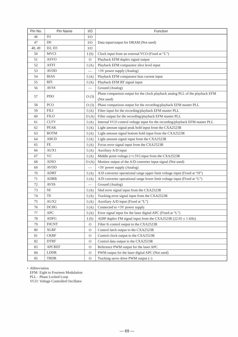
FunctionPin No. Pin Name I/O
46
47
48, 49
50
51
52
53
54
55
56
57
58
59
60
61
62
63
64
65
66
67
68
69
70
71
72
73
74
75
76
77
78
79
80
81
82
83
84
85
D1
D0
D2, D3
MVCI
ASYO
ASYI
AVDD
BIAS
RFI
AVSS
PDO
PCO
FILI
FILO
CLTV
PEAK
BOTM
ABCD
FE
AUX1
VC
ADIO
AVDD
ADRT
ADRB
AVSS
SE
TE
AUX2
DCHG
APC
ADFG
F0CNT
XLRF
CKRF
DTRF
APCREF
LDDR
TRDR
Data input/output for DRAM (Not used)
Clock input from an external VCO (Fixed at “L”)
Playback EFM duplex signal output
Playback EFM comparator slice level input
+3V power supply (Analog)
Playback EFM comparator bias current input
Playback EFM RF signal input
Ground (Analog)
Phase comparison output for the clock playback analog PLL of the playback EFM
(Not used)
Phase comparison output for the recording/playback EFM master PLL
Filter input for the recording/playback EFM master PLL
Filter output for the recording/playback EFM master PLL
Internal VCO control voltage input for the recording/playback EFM master PLL
Light amount signal peak hold input from the CXA2523R
Light amount signal bottom hold input from the CXA2523R
Light amount signal input from the CXA2523R
Focus error signal input from the CXA2523R
Auxiliary A/D input
Middle point voltage (+1.5V) input from the CXA2523R
Monitor output of the A/D converter input signal (Not used)
+3V power supply (Analog)
A/D converter operational range upper limit voltage input (Fixed at “H”)
A/D converter operational range lower limit voltage input (Fixed at “L”)
Ground (Analog)
Sled error signal input from the CXA2523R
Tracking error signal input from the CXA2523R
Auxiliary A/D input (Fixed at “L”)
Connected to +3V power supply
Error signal input for the laser digital APC (Fixed at “L”)
ADIP duplex FM signal input from the CXA2523R (22.05 ± 1 kHz)
Filter f0 control output to the CXA2523R
Control latch output to the CXA2523R
Control clock output to the CXA2523R
Control data output to the CXA2523R
Reference PWM output for the laser APC
PWM output for the laser digital APC (Not used)
Tracking servo drive PWM output (–)
I/O
I/O
I/O
I (S)
O
I (A)
—
I (A)
I (A)
—
O (3)
O (3)
I (A)
O (A)
I (A)
I (A)
I (A)
I (A)
I (A)
I (A)
I (A)
O (A)
—
I (A)
I (A)
—
I (A)
I (A)
I (A)
I (A)
I (A)
I (S)
O
O
O
O
O
O
O
• AbbreviationEFM: Eight to Fourteen ModulationPLL : Phase Locked LoopVCO: Voltage Controlled Oscillator
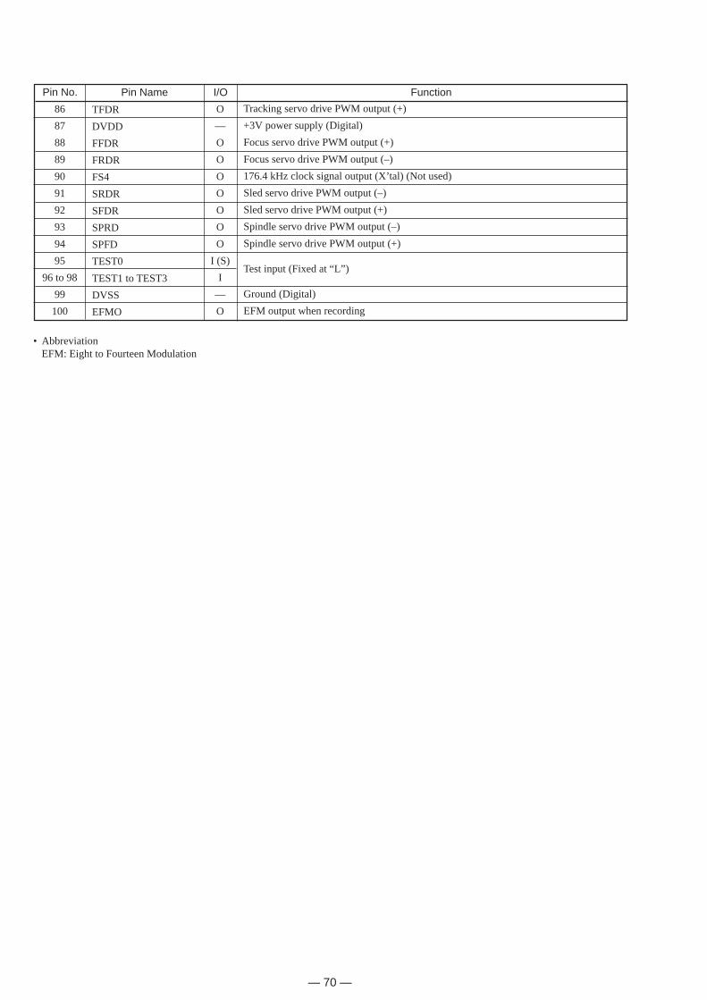
— 70 —
FunctionPin No. Pin Name I/O
86
87
88
89
90
91
92
93
94
95
96 to 98
99
100
TFDR
DVDD
FFDR
FRDR
FS4
SRDR
SFDR
SPRD
SPFD
TEST0
TEST1 to TEST3
DVSS
EFMO
O
—
O
O
O
O
O
O
O
I (S)
I
—
O
Tracking servo drive PWM output (+)
+3V power supply (Digital)
Focus servo drive PWM output (+)
Focus servo drive PWM output (–)
176.4 kHz clock signal output (X’tal) (Not used)
Sled servo drive PWM output (–)
Sled servo drive PWM output (+)
Spindle servo drive PWM output (–)
Spindle servo drive PWM output (+)
Test input (Fixed at “L”)
Ground (Digital)
EFM output when recording
• AbbreviationEFM: Eight to Fourteen Modulation
— 71 —
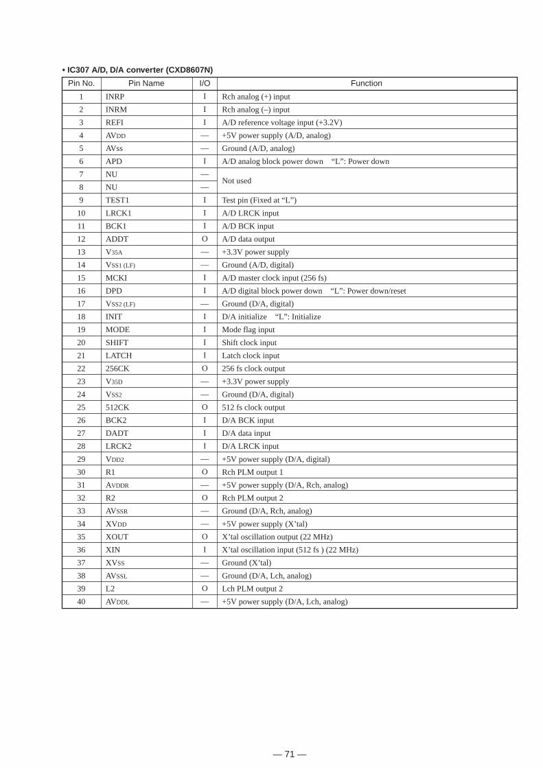
Pin No. Pin Name I/O Function
• IC307 A/D, D/A converter (CXD8607N)
1
2
3
4
5
6
7
8
9
10
11
12
13
14
15
16
17
18
19
20
21
22
23
24
25
26
27
28
29
30
31
32
33
34
35
36
37
38
39
40
INRP
INRM
REFI
AVDD
AVss
APD
NU
NU
TEST1
LRCK1
BCK1
ADDT
V35A
VSS1 (LF)
MCKI
DPD
VSS2 (LF)
INIT
MODE
SHIFT
LATCH
256CK
V35D
VSS2
512CK
BCK2
DADT
LRCK2
VDD2
R1
AVDDR
R2
AVSSR
XVDD
XOUT
XIN
XVSS
AVSSL
L2
AVDDL
I
I
I
—
—
I
—
—
I
I
I
O
—
—
I
I
—
I
I
I
I
O
—
—
O
I
I
I
—
O
—
O
—
—
O
I
—
—
O
—
Rch analog (+) input
Rch analog (–) input
A/D reference voltage input (+3.2V)
+5V power supply (A/D, analog)
Ground (A/D, analog)
A/D analog block power down “L”: Power down
Not used
Test pin (Fixed at “L”)
A/D LRCK input
A/D BCK input
A/D data output
+3.3V power supply
Ground (A/D, digital)
A/D master clock input (256 fs)
A/D digital block power down “L”: Power down/reset
Ground (D/A, digital)
D/A initialize “L”: Initialize
Mode flag input
Shift clock input
Latch clock input
256 fs clock output
+3.3V power supply
Ground (D/A, digital)
512 fs clock output
D/A BCK input
D/A data input
D/A LRCK input
+5V power supply (D/A, digital)
Rch PLM output 1
+5V power supply (D/A, Rch, analog)
Rch PLM output 2
Ground (D/A, Rch, analog)
+5V power supply (X’tal)
X’tal oscillation output (22 MHz)
X’tal oscillation input (512 fs ) (22 MHz)
Ground (X’tal)
Ground (D/A, Lch, analog)
Lch PLM output 2
+5V power supply (D/A, Lch, analog)
— 72 —
FunctionPin No. Pin Name I/O
41
42
43
44
45
46
47
48
49
50
51
52
53
54
55
56
L1
VDD2
VDD1
VDD1
VSS1
TEST2
TEST3
VSS1 (LF)
NU
NU
AVSS (LF)
LVDD
LVSS
REFO
INLM
INLP
O
—
—
—
—
I
I
—
—
—
—
—
—
O
I
I
Lch PLM output 1
+5V power supply (D/A, digital)
+5V power supply (A/D, digital)
Ground (A/D, digital)
Test pin (Fixed at “L”)
Ground (A/D, digital)
Not used
Ground (A/D, analog)
+5V power supply (A/D, buffer)
Ground (A/D, buffer)
A/D reference voltage output (+3.2V)
Lch analog (–) input
Lch analog (+) input
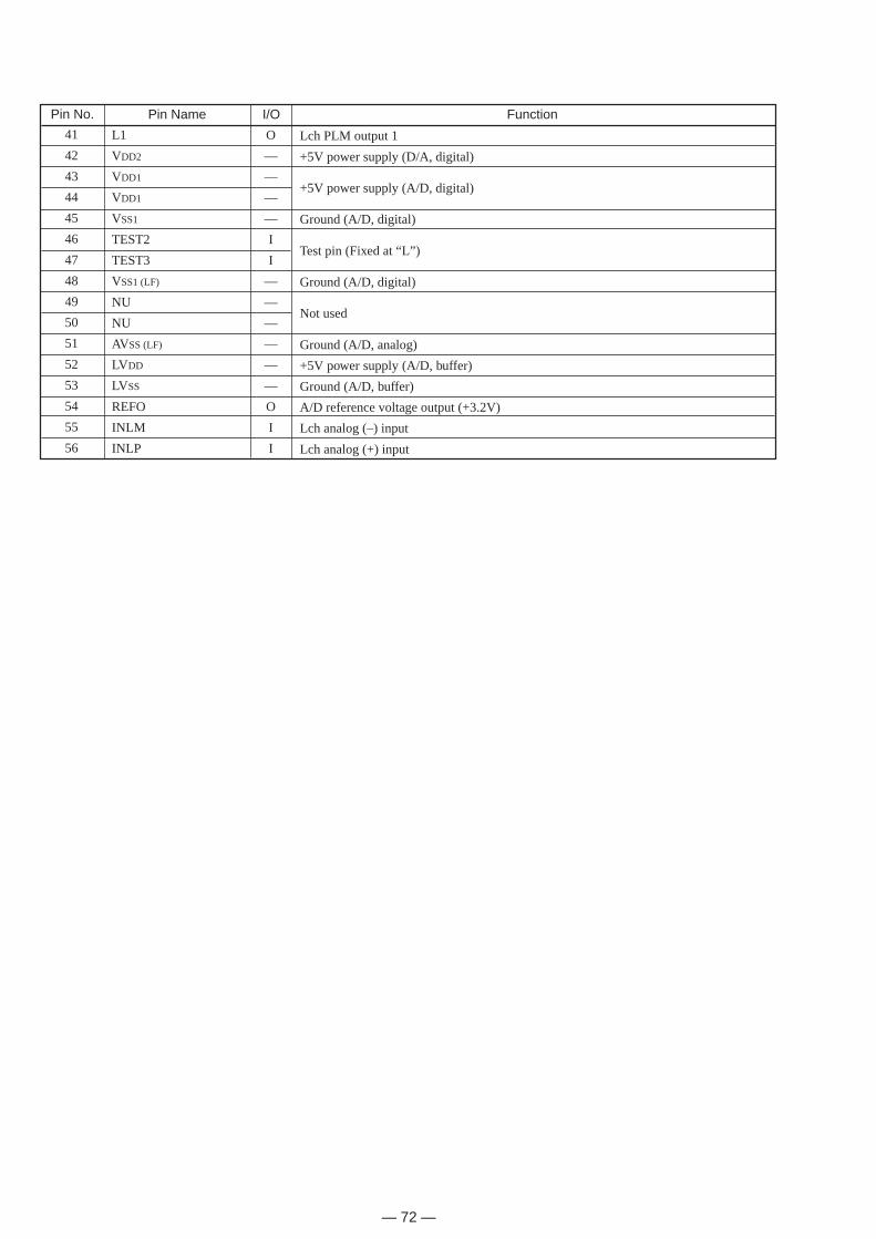
— 73 —
Pin No. Pin Name I/O Function
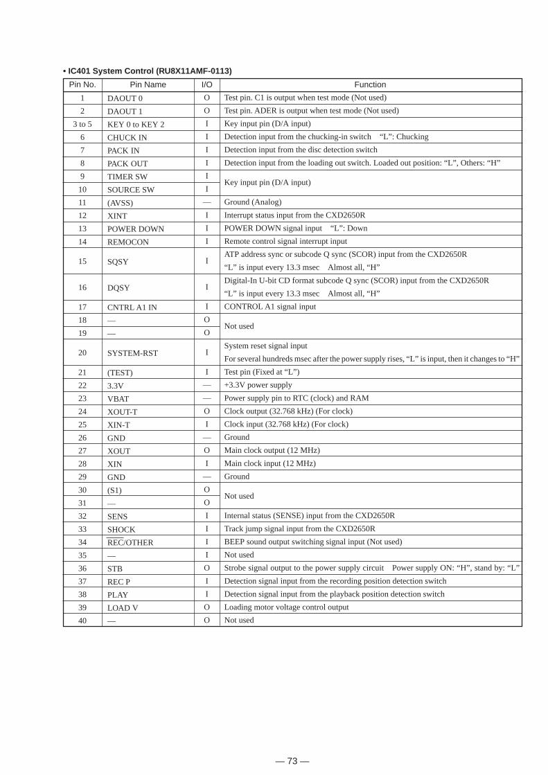
• IC401 System Control (RU8X11AMF-0113)
1
2
3 to 5
6
7
8
9
10
11
12
13
14
15
16
17
18
19
20
21
22
23
24
25
26
27
28
29
30
31
32
33
34
35
36
37
38
39
40
O
O
I
I
I
I
I
I
—
I
I
I
I
I
I
O
O
I
I
—
—
O
I
—
O
I
—
O
O
I
I
I
I
O
I
I
O
O
Test pin. C1 is output when test mode (Not used)
Test pin. ADER is output when test mode (Not used)
Key input pin (D/A input)
Detection input from the chucking-in switch “L”: Chucking
Detection input from the disc detection switch
Detection input from the loading out switch. Loaded out position: “L”, Others: “H”
Key input pin (D/A input)
Ground (Analog)
Interrupt status input from the CXD2650R
POWER DOWN signal input “L”: Down
Remote control signal interrupt input
ATP address sync or subcode Q sync (SCOR) input from the CXD2650R
“L” is input every 13.3 msec Almost all, “H”
Digital-In U-bit CD format subcode Q sync (SCOR) input from the CXD2650R
“L” is input every 13.3 msec Almost all, “H”
CONTROL A1 signal input
Not used
System reset signal input
For several hundreds msec after the power supply rises, “L” is input, then it changes to “H”
Test pin (Fixed at “L”)
+3.3V power supply
Power supply pin to RTC (clock) and RAM
Clock output (32.768 kHz) (For clock)
Clock input (32.768 kHz) (For clock)
Ground
Main clock output (12 MHz)
Main clock input (12 MHz)
Ground
Not used
Internal status (SENSE) input from the CXD2650R
Track jump signal input from the CXD2650R
BEEP sound output switching signal input (Not used)
Not used
Strobe signal output to the power supply circuit Power supply ON: “H”, stand by: “L”
Detection signal input from the recording position detection switch
Detection signal input from the playback position detection switch
Loading motor voltage control output
Not used
DAOUT 0
DAOUT 1
KEY 0 to KEY 2
CHUCK IN
PACK IN
PACK OUT
TIMER SW
SOURCE SW
(AVSS)
XINT
POWER DOWN
REMOCON
SQSY
DQSY
CNTRL A1 IN
—
—
SYSTEM-RST
(TEST)
3.3V
VBAT
XOUT-T
XIN-T
GND
XOUT
XIN
GND
(S1)
—
SENS
SHOCK
REC/OTHER
—
STB
REC P
PLAY
LOAD V
—
— 74 —
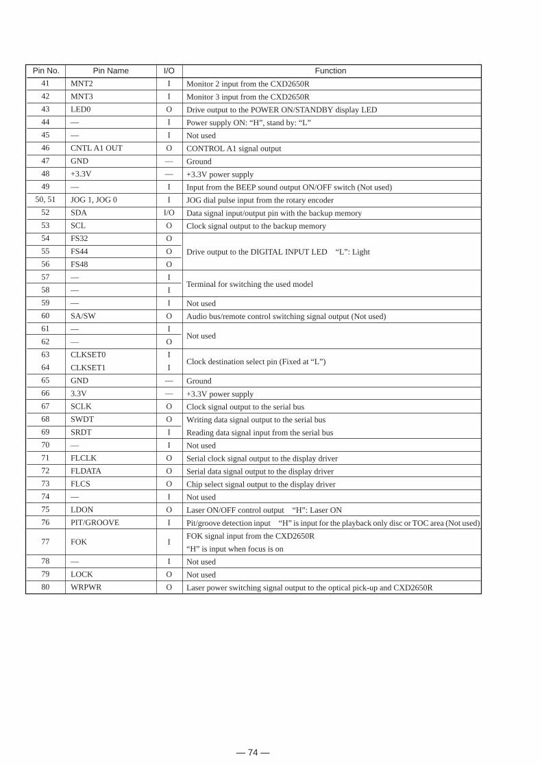
Pin No. Pin Name I/O Function
41
42
43
44
45
46
47
48
49
50, 51
52
53
54
55
56
57
58
59
60
61
62
63
64
65
66
67
68
69
70
71
72
73
74
75
76
77
78
79
80
MNT2
MNT3
LED0
—
—
CNTL A1 OUT
GND
+3.3V
—
JOG 1, JOG 0
SDA
SCL
FS32
FS44
FS48
—
—
—
SA/SW
—
—
CLKSET0
CLKSET1
GND
3.3V
SCLK
SWDT
SRDT
—
FLCLK
FLDATA
FLCS
—
LDON
PIT/GROOVE
FOK
—
LOCK
WRPWR
I
I
O
I
I
O
—
—
I
I
I/O
O
O
O
O
I
I
I
O
I
O
I
I
—
—
O
O
I
I
O
O
O
I
O
I
I
I
O
O
Monitor 2 input from the CXD2650R
Monitor 3 input from the CXD2650R
Drive output to the POWER ON/STANDBY display LED
Power supply ON: “H”, stand by: “L”
Not used
CONTROL A1 signal output
Ground
+3.3V power supply
Input from the BEEP sound output ON/OFF switch (Not used)
JOG dial pulse input from the rotary encoder
Data signal input/output pin with the backup memory
Clock signal output to the backup memory
Drive output to the DIGITAL INPUT LED “L”: Light
Terminal for switching the used model
Not used
Audio bus/remote control switching signal output (Not used)
Not used
Clock destination select pin (Fixed at “L”)
Ground
+3.3V power supply
Clock signal output to the serial bus
Writing data signal output to the serial bus
Reading data signal input from the serial bus
Not used
Serial clock signal output to the display driver
Serial data signal output to the display driver
Chip select signal output to the display driver
Not used
Laser ON/OFF control output “H”: Laser ON
Pit/groove detection input “H” is input for the playback only disc or TOC area (Not used)
FOK signal input from the CXD2650R
“H” is input when focus is on
Not used
Not used
Laser power switching signal output to the optical pick-up and CXD2650R
— 75 —
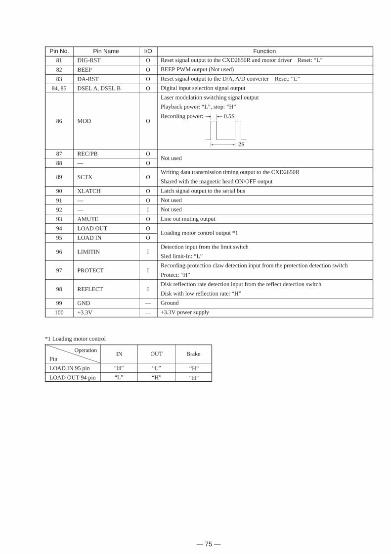
Pin No. Pin Name I/O Function
81
82
83
84, 85
86
87
88
89
90
91
92
93
94
95
96
97
98
99
100
DIG-RST
BEEP
DA-RST
DSEL A, DSEL B
MOD
REC/PB
—
SCTX
XLATCH
—
—
AMUTE
LOAD OUT
LOAD IN
LIMITIN
PROTECT
REFLECT
GND
+3.3V
O
O
O
O
O
O
O
O
O
O
I
O
O
O
I
I
I
—
—
0.5S
2S
Reset signal output to the CXD2650R and motor driver Reset: “L”
BEEP PWM output (Not used)
Reset signal output to the D/A, A/D converter Reset: “L”
Digital input selection signal output
Laser modulation switching signal output
Playback power: “L”, stop: “H”
Recording power:
Not used
Writing data transmission timing output to the CXD2650R
Shared with the magnetic head ON/OFF output
Latch signal output to the serial bus
Not used
Not used
Line out muting output
Loading motor control output *1
Detection input from the limit switch
Sled limit-In: “L”
Recording-protection claw detection input from the protection detection switch
Protect: “H”
Disk reflection rate detection input from the reflect detection switch
Disk with low reflection rate: “H”
Ground
+3.3V power supply
Pin
LOAD IN 95 pin
LOAD OUT 94 pin
OperationIN
“H”
“L”
OUT Brake
“L”
“H”
“H”
“H”
*1 Loading motor control
— 76 —
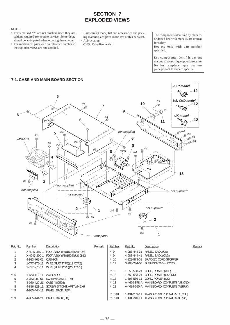
Ref. No. Part No. Description Remark
* 9 4-985-444-31 PANEL, BACK (US)* 9 4-985-444-41 PANEL, BACK (CND)* 10 4-923-873-01 BRACKET, CORD STOPPER* 11 3-703-244-00 BUSHING (2104), CORD
!12 1-558-568-21 CORD, POWER (AEP)!12 1-559-583-21 CORD, POWER (US,CND)!12 1-696-586-11 CORD, POWER (UK)* 13 A-4699-578-A MAIN BOARD, COMPLETE (US,CND)* 13 A-4699-585-A MAIN BOARD, COMPLETE (AEP,UK)
!T901 1-431-239-11 TRANSFORMER, POWER (US,CND)!T901 1-431-240-11 TRANSFORMER, POWER (AEP,UK)
SECTION 7EXPLODED VIEWS
NOTE:• Items marked “*” are not stocked since they are
seldom required for routine service. Some delayshould be anticipated when ordering these items.
• The mechanical parts with no reference number inthe exploded views are not supplied.
• Hardware (# mark) list and accessories and pack-ing materials are given in the last of this parts list.
• AbbreviationCND : Canadian model
The components identified by mark !or dotted line with mark ! are criticalfor safety.Replace only with part numberspecified.
Les composants identifiés par unemarque ! sont critiques pour la sécurité.Ne les remplacer que par unepiéce portant le numéro spécifié.
7-1. CASE AND MAIN BOARD SECTION
Ref. No. Part No. Description Remark
1 X-4947-389-1 FOOT ASSY (F50150S)(AEP,UK)1 X-4947-390-1 FOOT ASSY (F50150S)(US,CND)2 4-983-762-02 CUSHION3 1-777-278-11 WIRE (FLAT TYPE)(19 CORE)4 1-777-275-11 WIRE (FLAT TYPE)(29 CORE)
* 5 1-663-118-11 AC BOARD6 3-363-099-01 SCREW (CASE 3 TP2)7 4-980-420-21 CASE (409526)8 4-886-821-11 SCREW, S TIGHT, +PTTWH 3X6
* 9 4-985-444-11 PANEL, BACK (AEP)
* 9 4-985-444-21 PANEL, BACK (UK)
#4
#4
6
not supplied
AEP model
12
US, CND model12
UK model12
#4
11
10
#4#4
#4#4
#3#5
#5MDM-3A
5 #4
#4
6
6
7
6
#4
not supplied
2
1#4
#4#4
Front panel
#4
2
not supplied
#4#4T901
13
not supplied
not supplied
not supplied
#1 3
4
1
8
8
9
#4
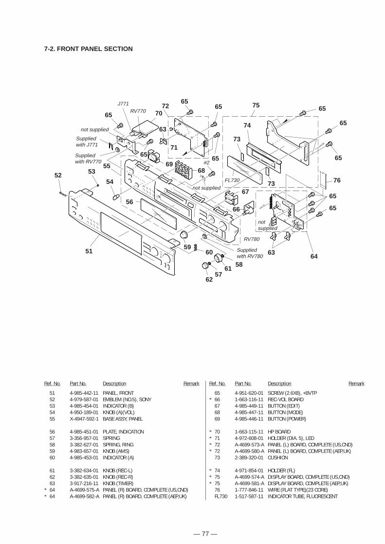
— 77 —
7-2. FRONT PANEL SECTION
65
#2
6572
70
65
6955
Suppliedwith RV770
Suppliedwith J771
not supplied
61
6351
68
not suppliedFL730
52 53
54
56
5960
6257
58
Suppliedwith RV780
RV780
66
67
65
65
7673
65
65
6575
74
73
65
65
71
RV770J771
64
Ref. No. Part No. Description Remark
51 4-985-442-11 PANEL, FRONT52 4-979-587-01 EMBLEM (NO.5), SONY53 4-985-454-01 INDICATOR (B)54 4-950-189-01 KNOB (A)(VOL)55 X-4947-592-1 BASE ASSY, PANEL
56 4-985-451-01 PLATE, INDICATION57 3-356-957-01 SPRING58 3-382-627-01 SPRING, RING59 4-983-657-01 KNOB (AMS)60 4-985-453-01 INDICATOR (A)
61 3-382-634-01 KNOB (REC-L)62 3-382-635-01 KNOB (REC-R)63 3-917-216-11 KNOB (TIMER)
* 64 A-4699-575-A PANEL (R) BOARD, COMPLETE (US,CND)* 64 A-4699-582-A PANEL (R) BOARD, COMPLETE (AEP,UK)
Ref. No. Part No. Description Remark
65 4-951-620-01 SCREW (2.6X8), +BVTP* 66 1-663-116-11 REC-VOL BOARD
67 4-985-449-11 BUTTON (EDIT)68 4-985-447-11 BUTTON (MODE)69 4-985-446-11 BUTTON (POWER)
* 70 1-663-115-11 HP BOARD* 71 4-972-608-01 HOLDER (DIA. 5), LED* 72 A-4699-573-A PANEL (L) BOARD, COMPLETE (US,CND)* 72 A-4699-580-A PANEL (L) BOARD, COMPLETE (AEP,UK)
73 2-389-320-01 CUSHION
* 74 4-971-854-01 HOLDER (FL)* 75 A-4699-574-A DISPLAY BOARD, COMPLETE (US,CND)* 75 A-4699-581-A DISPLAY BOARD, COMPLETE (AEP,UK)
76 1-777-846-11 WIRE (FLAT TYPE)(23 CORE)FL730 1-517-587-11 INDICATOR TUBE, FLUORESCENT
notsupplied
63
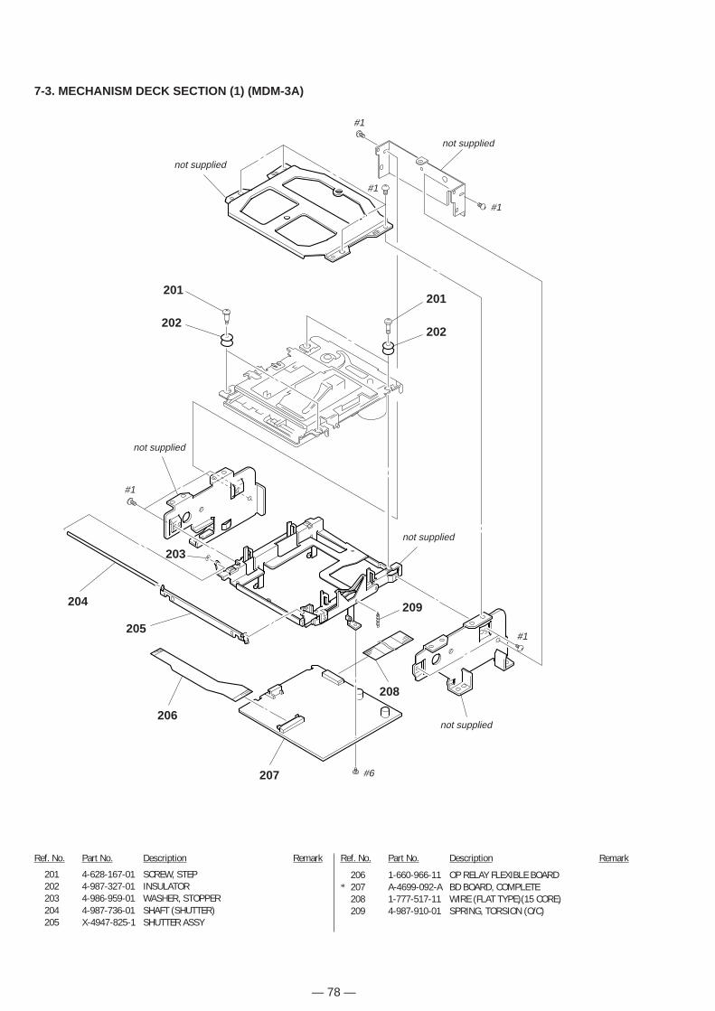
— 78 —
#1
7-3. MECHANISM DECK SECTION (1) (MDM-3A)
not supplied
not supplied
#1
#1
201
202
201
202
not supplied
#1
206
207 #6
208
not supplied
not supplied
209
203
205#1
204
Ref. No. Part No. Description Remark
201 4-628-167-01 SCREW, STEP202 4-987-327-01 INSULATOR203 4-986-959-01 WASHER, STOPPER204 4-987-736-01 SHAFT (SHUTTER)205 X-4947-825-1 SHUTTER ASSY
Ref. No. Part No. Description Remark
206 1-660-966-11 OP RELAY FLEXIBLE BOARD* 207 A-4699-092-A BD BOARD, COMPLETE
208 1-777-517-11 WIRE (FLAT TYPE)(15 CORE)209 4-987-910-01 SPRING, TORSION (O/C)
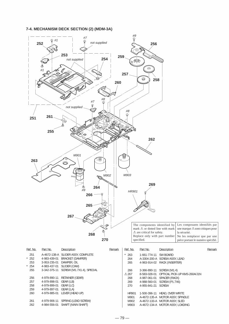
— 79 —
7-4. MECHANISM DECK SECTION (2) (MDM-3A)
Ref. No. Part No. Description Remark Ref. No. Part No. Description Remark
* 263 1-661-774-11 SW BOARD264 A-3304-200-A SCREW ASSY, LEAD265 4-963-914-02 RACK (INSERTER)
266 3-366-890-11 SCREW (M1.4)!267 8-583-028-01 OPTICAL PICK-UP KMS-260A/J1N
268 4-987-061-01 SPACER (RACK)269 4-988-560-01 SCREW (P1.7X6)270 4-955-841-21 SCREW
HR901 1-500-396-11 HEAD, OVER WRITEM901 A-4672-135-A MOTOR ASSY, SPINDLEM902 A-4672-133-A MOTOR ASSY, SLEDM903 A-4672-134-A MOTOR ASSY, LOADING
251 A-4672-138-A SLIDER ASSY, COMPLETE* 252 4-983-439-01 BRACKET (DAMPER)
253 3-953-235-01 DAMPER, OIL* 254 4-983-437-01 SLIDER (CAM)
255 3-342-375-11 SCREW (M1.7X1.4), SPECIAL
256 4-979-890-11 RETAINER (GEAR)257 4-979-898-01 GEAR (LB)258 4-979-899-01 GEAR (LC)259 4-979-897-01 GEAR (LA)260 4-979-885-01 LEVER (HEAD UP)
261 4-979-906-11 SPRING (LEAD SCREW)262 4-984-556-01 SHAFT (MAIN SHAFT)
256#1
252
253
#1
#7
not supplied
#9
259254
257
260
#8
258
#8#7
not supplied
261251
255
263M901
M902 M903
262
264
266
265
267
268270
HR901
269
Les composants identifiés parune marque ! sont critiques pourla sécurité.Ne les remplacer que par unepiéce portant le numéro spécifié.
The components identified bymark ! or dotted line with mark! are critical for safety.Replace only with part numberspecified.
#9
not supplied
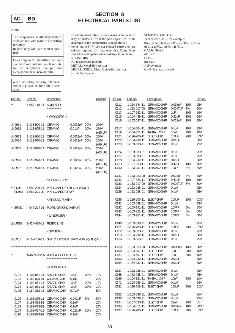
— 80 —
Ref. No. Part No. Description Remark
* 1-663-118-11 AC BOARD*********
< CAPACITOR >
!C951 1-113-920-11 CERAMIC 0.0022uF 20% 250V!C952 1-113-925-11 CERAMIC 0.01uF 20% 250V
(AEP,UK)!C953 1-113-920-11 CERAMIC 0.0022uF 20% 250V!C954 1-113-920-11 CERAMIC 0.0022uF 20% 250V
(AEP,UK)!C955 1-113-920-11 CERAMIC 0.0022uF 20% 250V
(AEP,UK)
!C956 1-113-920-11 CERAMIC 0.0022uF 20% 250V(AEP,UK)
!C957 1-113-920-11 CERAMIC 0.0022uF 20% 250V(AEP,UK)
< CONNECTOR >
* CN951 1-580-230-21 PIN, CONNECTOR (PC BOARD) 2PCN952 1-564-321-00 PIN, CONNECTOR 2P
< GROUND PLATE >
* EP951 4-942-204-01 PLATE, GROUND (AEP,UK)
< LINE FILTER >
!LF951 1-424-485-11 FILTER, LINE
< SWITCH >
!S951 1-762-764-11 SWITCH, POWER (MAIN POWER)(AEP,UK)
**************************************************************
* A-4699-092-A BD BOARD, COMPLETE*******************
< CAPACITOR >
C101 1-104-851-11 TANTAL. CHIP 10uF 20% 10VC102 1-163-038-91 CERAMIC CHIP 0.1uF 25VC103 1-104-851-11 TANTAL. CHIP 10uF 20% 10VC104 1-104-851-11 TANTAL. CHIP 10uF 20% 10VC105 1-164-232-11 CERAMIC CHIP 0.01uF 50V
C106 1-163-275-11 CERAMIC CHIP 0.001uF 5% 50VC107 1-163-038-91 CERAMIC CHIP 0.1uF 25VC108 1-163-038-91 CERAMIC CHIP 0.1uF 25VC109 1-163-037-11 CERAMIC CHIP 0.022uF 10% 25VC110 1-163-038-91 CERAMIC CHIP 0.1uF 25V
Ref. No. Part No. Description Remark
C111 1-164-344-11 CERAMIC CHIP 0.068uF 10% 25VC112 1-163-017-00 CERAMIC CHIP 0.0047uF 5% 50VC113 1-107-682-11 CERAMIC CHIP 1uF 10% 16VC115 1-164-489-11 CERAMIC CHIP 0.22uF 10% 16VC116 1-163-037-11 CERAMIC CHIP 0.022uF 10% 25V
C117 1-164-004-11 CERAMIC CHIP 0.1uF 10% 25VC119 1-104-851-11 TANTAL. CHIP 10uF 20% 10VC121 1-126-206-11 ELECT CHIP 100uF 20% 6.3VC122 1-164-232-11 CERAMIC CHIP 0.01uF 50VC123 1-163-038-91 CERAMIC CHIP 0.1uF 25V
C124 1-163-038-91 CERAMIC CHIP 0.1uF 25VC127 1-163-038-91 CERAMIC CHIP 0.1uF 25VC128 1-164-232-11 CERAMIC CHIP 0.01uF 50VC129 1-107-823-11 CERAMIC CHIP 0.47uF 10% 16VC130 1-163-251-11 CERAMIC CHIP 100PF 5% 50V
C131 1-163-023-00 CERAMIC CHIP 0.015uF 5% 50VC132 1-107-823-11 CERAMIC CHIP 0.47uF 10% 16VC133 1-163-017-00 CERAMIC CHIP 0.0047uF 5% 50VC134 1-163-038-91 CERAMIC CHIP 0.1uF 25VC135 1-163-038-91 CERAMIC CHIP 0.1uF 25V
C136 1-126-206-11 ELECT CHIP 100uF 20% 6.3VC141 1-163-038-91 CERAMIC CHIP 0.1uF 25VC142 1-163-251-11 CERAMIC CHIP 100PF 5% 50VC143 1-163-251-11 CERAMIC CHIP 100PF 5% 50VC144 1-163-251-11 CERAMIC CHIP 100PF 5% 50V
C146 1-163-038-91 CERAMIC CHIP 0.1uF 25VC151 1-126-206-11 ELECT CHIP 100uF 20% 6.3VC152 1-163-038-91 CERAMIC CHIP 0.1uF 25VC153 1-164-232-11 CERAMIC CHIP 0.01uF 50VC156 1-163-038-91 CERAMIC CHIP 0.1uF 25V
C158 1-163-019-00 CERAMIC CHIP 0.0068uF 10% 50VC160 1-104-601-11 ELECT CHIP 10uF 20% 10VC161 1-104-601-11 ELECT CHIP 10uF 20% 10VC163 1-164-232-11 CERAMIC CHIP 0.01uF 50VC164 1-164-232-11 CERAMIC CHIP 0.01uF 50V
C167 1-163-038-91 CERAMIC CHIP 0.1uF 25VC168 1-163-038-91 CERAMIC CHIP 0.1uF 25VC169 1-104-851-11 TANTAL. CHIP 10uF 20% 10VC171 1-163-038-91 CERAMIC CHIP 0.1uF 25VC181 1-126-206-11 ELECT CHIP 100uF 20% 6.3V
C182 1-163-038-91 CERAMIC CHIP 0.1uF 25VC183 1-163-038-91 CERAMIC CHIP 0.1uF 25VC184 1-107-836-11 ELECT CHIP 22uF 20% 8VC185 1-164-611-11 CERAMIC CHIP 0.001uF 10% 500VC187 1-126-206-11 ELECT CHIP 100uF 20% 6.3V
SECTION 8ELECTRICAL PARTS LISTAC BD
The components identified by mark !or dotted line with mark ! are criticalfor safety.Replace only with part number speci-fied.
Les composants identifiés par unemarque ! sont critiques pour la sécurité.Ne les remplacer que par unepiéce portant le numéro spécifié.
When indicating parts by referencenumber, please include the boardname.
• SEMICONDUCTORSIn each case, u: µ , for example:uA...: µ A..., uPA...: µ PA..., uPB...: µ PB...,uPC...: µ PC..., uPD...: µ PD...
• CAPACITORSuF : µ F
• COILSuH : µ H
• AbbreviationCND : Canadian model
• Due to standardization, replacements in the parts listmay be different from the parts specified in thediagrams or the components used on the set.
• Items marked “*” are not stocked since they areseldom required for routine service. Some delayshould be anticipated when ordering these items.
• RESISTORSAll resistors are in ohmsMETAL: Metal-film resistorMETAL OXIDE: Metal Oxide-film resistorF : nonflammable
Note:
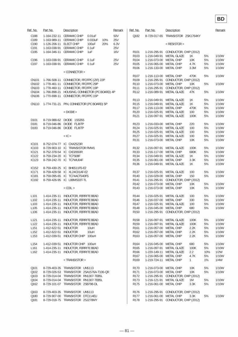
— 81 —
BD
Ref. No. Part No. Description Remark
C188 1-164-232-11 CERAMIC CHIP 0.01uF 50VC189 1-163-989-11 CERAMIC CHIP 0.033uF 10% 25VC190 1-126-206-11 ELECT CHIP 100uF 20% 6.3VC191 1-163-038-91 CERAMIC CHIP 0.1uF 25VC195 1-164-346-11 CERAMIC CHIP 1uF 16V
C196 1-163-038-91 CERAMIC CHIP 0.1uF 25VC197 1-163-038-91 CERAMIC CHIP 0.1uF 25V
< CONNECTOR >
CN101 1-766-508-11 CONNECTOR, FFC/FPC (ZIF) 22PCN102 1-778-461-11 CONNECTOR, FFC/FPC 29PCN103 1-778-460-11 CONNECTOR, FFC/FPC 19PCN104 1-766-898-21 HOUSING, CONNECTOR (PC BOARD) 4PCN106 1-770-698-11 CONNECTOR, FFC/FPC 15P
CN110 1-774-731-21 PIN, CONNECTOR (PC BOARD) 5P
< DIODE >
D101 8-719-988-62 DIODE 1SS355D181 8-719-046-86 DIODE F1J6TPD183 8-719-046-86 DIODE F1J6TP
< IC >
IC101 8-752-074-77 IC CXA2523RIC103 8-729-903-10 IC TRANSISTOR FMW1IC121 8-752-378-54 IC CXD2650RIC122 8-759-234-20 IC TC7S08FIC123 8-759-242-70 IC TC7WU04F
IC152 8-759-430-25 IC BH6511FS-E2IC171 8-759-428-58 IC XL24C01AF-E2IC181 8-759-095-65 IC TC74ACT540FSIC192 8-759-426-95 IC L88MS33T-TL
< COIL >
L101 1-414-235-11 INDUCTOR, FERRITE BEADL102 1-414-235-11 INDUCTOR, FERRITE BEADL103 1-414-235-11 INDUCTOR, FERRITE BEADL105 1-414-235-11 INDUCTOR, FERRITE BEADL106 1-414-235-11 INDUCTOR, FERRITE BEAD
L121 1-414-235-11 INDUCTOR, FERRITE BEADL122 1-414-235-11 INDUCTOR, FERRITE BEADL151 1-412-622-51 INDUCTOR 10uHL152 1-412-622-51 INDUCTOR 10uHL153 1-412-039-51 INDUCTOR CHIP 100uH
L154 1-412-039-51 INDUCTOR CHIP 100uHL161 1-414-235-11 INDUCTOR, FERRITE BEADL162 1-414-235-11 INDUCTOR, FERRITE BEAD
< TRANSISTOR >
Q101 8-729-403-35 TRANSISTOR UN5113Q102 8-729-026-53 TRANSISTOR 2SA1576A-T106-QRQ103 8-729-014-04 TRANSISTOR RN1307-TE85LQ104 8-729-014-04 TRANSISTOR RN1307-TE85LQ162 8-729-101-07 TRANSISTOR 2SB798-DL
Q163 8-729-403-35 TRANSISTOR UN5113Q180 8-729-907-00 TRANSISTOR DTC114EUQ181 8-729-018-75 TRANSISTOR 2SJ278MY
Ref. No. Part No. Description Remark
Q182 8-729-017-65 TRANSISTOR 2SK1764KY
< RESISTOR >
R101 1-216-295-91 CONDUCTOR, CHIP (2012)R103 1-216-049-91 METAL GLAZE 1K 5% 1/10WR104 1-216-073-00 METAL CHIP 10K 5% 1/10WR105 1-216-065-00 METAL CHIP 4.7K 5% 1/10WR106 1-216-133-00 METAL CHIP 3.3M 5% 1/10W
R107 1-216-113-00 METAL CHIP 470K 5% 1/10WR109 1-216-295-91 CONDUCTOR, CHIP (2012)R110 1-216-073-00 METAL CHIP 10K 5% 1/10WR111 1-216-295-91 CONDUCTOR, CHIP (2012)R112 1-216-089-91 METAL GLAZE 47K 5% 1/10W
R113 1-216-049-91 METAL GLAZE 1K 5% 1/10WR115 1-216-049-91 METAL GLAZE 1K 5% 1/10WR117 1-216-113-00 METAL CHIP 470K 5% 1/10WR120 1-216-025-91 METAL GLAZE 100 5% 1/10WR121 1-216-097-91 METAL GLAZE 100K 5% 1/10W
R123 1-216-033-00 METAL CHIP 220 5% 1/10WR124 1-216-025-91 METAL GLAZE 100 5% 1/10WR125 1-216-025-91 METAL GLAZE 100 5% 1/10WR127 1-216-025-91 METAL GLAZE 100 5% 1/10WR131 1-216-073-00 METAL CHIP 10K 5% 1/10W
R132 1-216-097-91 METAL GLAZE 100K 5% 1/10WR133 1-216-117-00 METAL CHIP 680K 5% 1/10WR134 1-216-049-91 METAL GLAZE 1K 5% 1/10WR135 1-216-061-00 METAL CHIP 3.3K 5% 1/10WR136 1-216-049-91 METAL GLAZE 1K 5% 1/10W
R137 1-216-025-91 METAL GLAZE 100 5% 1/10WR140 1-216-029-00 METAL CHIP 150 5% 1/10WR141 1-216-295-91 CONDUCTOR, CHIP (2012)R142 1-216-073-00 METAL CHIP 10K 5% 1/10WR143 1-216-073-00 METAL CHIP 10K 5% 1/10W
R144 1-216-025-91 METAL GLAZE 100 5% 1/10WR146 1-216-037-00 METAL CHIP 330 5% 1/10WR147 1-216-025-91 METAL GLAZE 100 5% 1/10WR148 1-216-045-00 METAL CHIP 680 5% 1/10WR150 1-216-295-91 CONDUCTOR, CHIP (2012)
R158 1-216-097-91 METAL GLAZE 100K 5% 1/10WR159 1-216-097-91 METAL GLAZE 100K 5% 1/10WR161 1-216-057-00 METAL CHIP 2.2K 5% 1/10WR162 1-216-057-00 METAL CHIP 2.2K 5% 1/10WR163 1-216-057-00 METAL CHIP 2.2K 5% 1/10W
R164 1-216-045-00 METAL CHIP 680 5% 1/10WR165 1-216-097-91 METAL GLAZE 100K 5% 1/10WR166 1-220-149-11 METAL GLAZE 2.2 10% 1/2WR167 1-216-065-00 METAL CHIP 4.7K 5% 1/10WR169 1-219-724-11 METAL CHIP 1 1% 1/4W
R170 1-216-073-00 METAL CHIP 10K 5% 1/10WR171 1-216-073-00 METAL CHIP 10K 5% 1/10WR172 1-216-295-91 CONDUCTOR, CHIP (2012)R173 1-216-121-91 METAL GLAZE 1M 5% 1/10WR175 1-216-061-00 METAL CHIP 3.3K 5% 1/10W
R176 1-216-295-91 CONDUCTOR, CHIP (2012)R177 1-216-061-00 METAL CHIP 3.3K 5% 1/10WR178 1-216-295-91 CONDUCTOR, CHIP (2012)
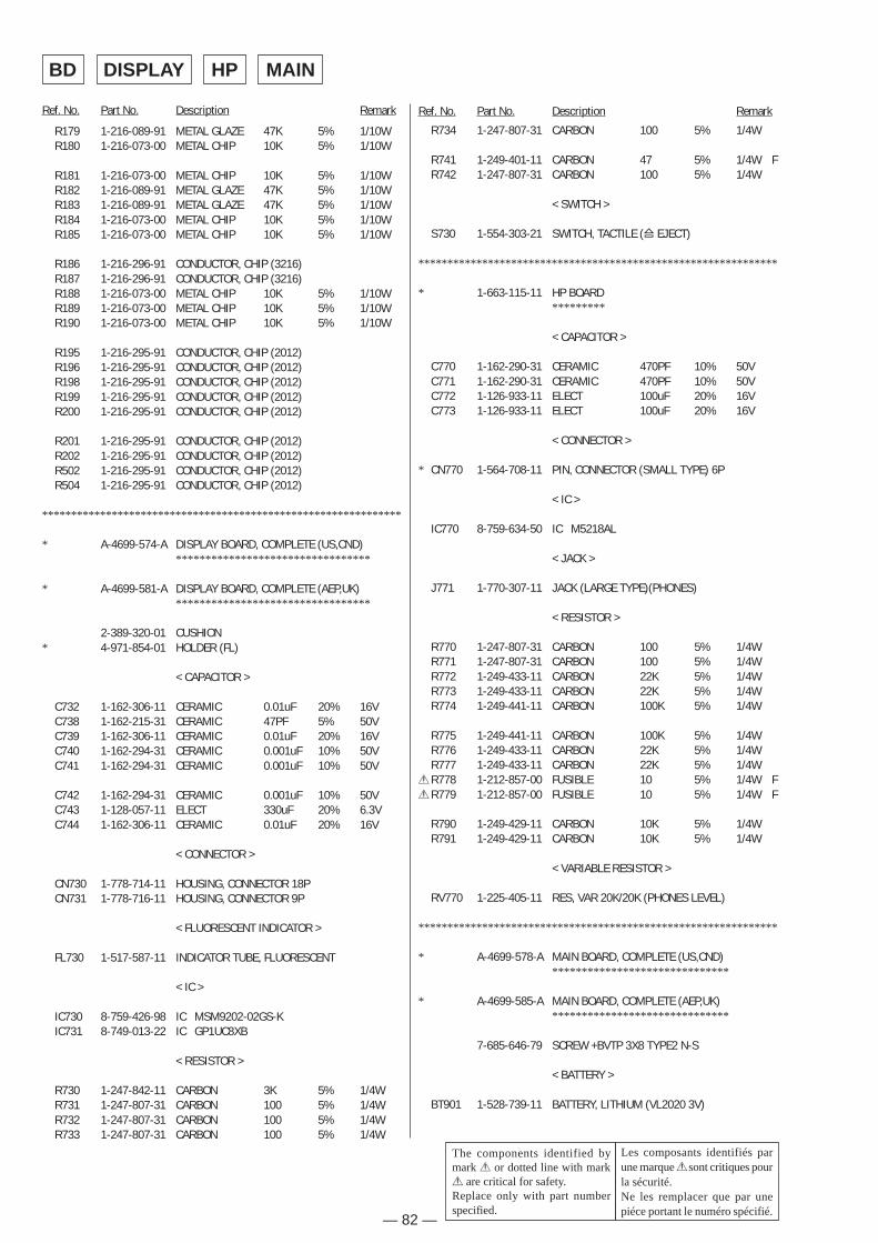
— 82 —
BD DISPLAY HP
Ref. No. Part No. Description Remark
R179 1-216-089-91 METAL GLAZE 47K 5% 1/10WR180 1-216-073-00 METAL CHIP 10K 5% 1/10W
R181 1-216-073-00 METAL CHIP 10K 5% 1/10WR182 1-216-089-91 METAL GLAZE 47K 5% 1/10WR183 1-216-089-91 METAL GLAZE 47K 5% 1/10WR184 1-216-073-00 METAL CHIP 10K 5% 1/10WR185 1-216-073-00 METAL CHIP 10K 5% 1/10W
R186 1-216-296-91 CONDUCTOR, CHIP (3216)R187 1-216-296-91 CONDUCTOR, CHIP (3216)R188 1-216-073-00 METAL CHIP 10K 5% 1/10WR189 1-216-073-00 METAL CHIP 10K 5% 1/10WR190 1-216-073-00 METAL CHIP 10K 5% 1/10W
R195 1-216-295-91 CONDUCTOR, CHIP (2012)R196 1-216-295-91 CONDUCTOR, CHIP (2012)R198 1-216-295-91 CONDUCTOR, CHIP (2012)R199 1-216-295-91 CONDUCTOR, CHIP (2012)R200 1-216-295-91 CONDUCTOR, CHIP (2012)
R201 1-216-295-91 CONDUCTOR, CHIP (2012)R202 1-216-295-91 CONDUCTOR, CHIP (2012)R502 1-216-295-91 CONDUCTOR, CHIP (2012)R504 1-216-295-91 CONDUCTOR, CHIP (2012)
**************************************************************
* A-4699-574-A DISPLAY BOARD, COMPLETE (US,CND)*********************************
* A-4699-581-A DISPLAY BOARD, COMPLETE (AEP,UK)*********************************
2-389-320-01 CUSHION* 4-971-854-01 HOLDER (FL)
< CAPACITOR >
C732 1-162-306-11 CERAMIC 0.01uF 20% 16VC738 1-162-215-31 CERAMIC 47PF 5% 50VC739 1-162-306-11 CERAMIC 0.01uF 20% 16VC740 1-162-294-31 CERAMIC 0.001uF 10% 50VC741 1-162-294-31 CERAMIC 0.001uF 10% 50V
C742 1-162-294-31 CERAMIC 0.001uF 10% 50VC743 1-128-057-11 ELECT 330uF 20% 6.3VC744 1-162-306-11 CERAMIC 0.01uF 20% 16V
< CONNECTOR >
CN730 1-778-714-11 HOUSING, CONNECTOR 18PCN731 1-778-716-11 HOUSING, CONNECTOR 9P
< FLUORESCENT INDICATOR >
FL730 1-517-587-11 INDICATOR TUBE, FLUORESCENT
< IC >
IC730 8-759-426-98 IC MSM9202-02GS-KIC731 8-749-013-22 IC GP1UC8XB
< RESISTOR >
R730 1-247-842-11 CARBON 3K 5% 1/4WR731 1-247-807-31 CARBON 100 5% 1/4WR732 1-247-807-31 CARBON 100 5% 1/4WR733 1-247-807-31 CARBON 100 5% 1/4W
Ref. No. Part No. Description Remark
R734 1-247-807-31 CARBON 100 5% 1/4W
R741 1-249-401-11 CARBON 47 5% 1/4W FR742 1-247-807-31 CARBON 100 5% 1/4W
< SWITCH >
S730 1-554-303-21 SWITCH, TACTILE (§ EJECT)
**************************************************************
* 1-663-115-11 HP BOARD*********
< CAPACITOR >
C770 1-162-290-31 CERAMIC 470PF 10% 50VC771 1-162-290-31 CERAMIC 470PF 10% 50VC772 1-126-933-11 ELECT 100uF 20% 16VC773 1-126-933-11 ELECT 100uF 20% 16V
< CONNECTOR >
* CN770 1-564-708-11 PIN, CONNECTOR (SMALL TYPE) 6P
< IC >
IC770 8-759-634-50 IC M5218AL
< JACK >
J771 1-770-307-11 JACK (LARGE TYPE)(PHONES)
< RESISTOR >
R770 1-247-807-31 CARBON 100 5% 1/4WR771 1-247-807-31 CARBON 100 5% 1/4WR772 1-249-433-11 CARBON 22K 5% 1/4WR773 1-249-433-11 CARBON 22K 5% 1/4WR774 1-249-441-11 CARBON 100K 5% 1/4W
R775 1-249-441-11 CARBON 100K 5% 1/4WR776 1-249-433-11 CARBON 22K 5% 1/4WR777 1-249-433-11 CARBON 22K 5% 1/4W!R778 1-212-857-00 FUSIBLE 10 5% 1/4W F!R779 1-212-857-00 FUSIBLE 10 5% 1/4W F
R790 1-249-429-11 CARBON 10K 5% 1/4WR791 1-249-429-11 CARBON 10K 5% 1/4W
< VARIABLE RESISTOR >
RV770 1-225-405-11 RES, VAR 20K/20K (PHONES LEVEL)
**************************************************************
* A-4699-578-A MAIN BOARD, COMPLETE (US,CND)******************************
* A-4699-585-A MAIN BOARD, COMPLETE (AEP,UK)******************************
7-685-646-79 SCREW +BVTP 3X8 TYPE2 N-S
< BATTERY >
BT901 1-528-739-11 BATTERY, LITHIUM (VL2020 3V)
MAIN
Les composants identifiés parune marque ! sont critiques pourla sécurité.Ne les remplacer que par unepiéce portant le numéro spécifié.
The components identified bymark ! or dotted line with mark! are critical for safety.Replace only with part numberspecified.
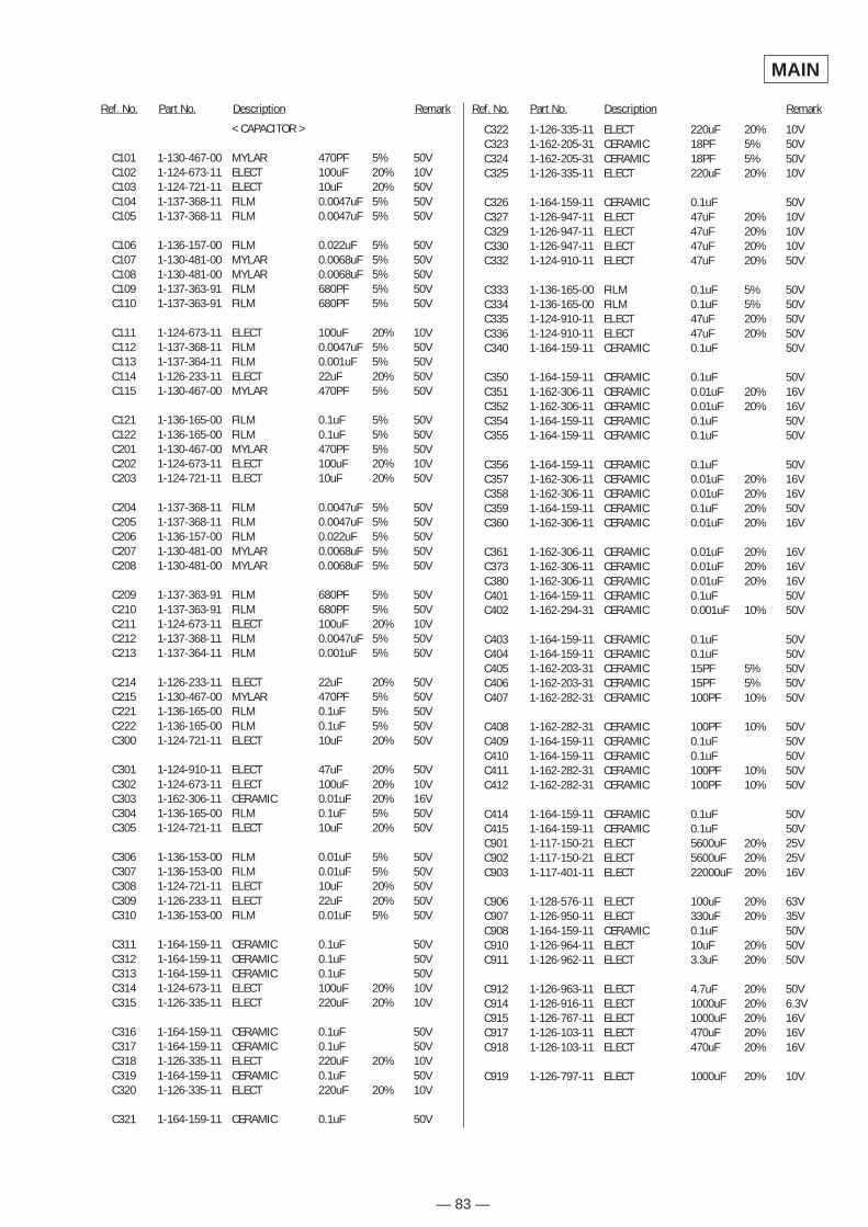
— 83 —
MAIN
Ref. No. Part No. Description Remark
< CAPACITOR >
C101 1-130-467-00 MYLAR 470PF 5% 50VC102 1-124-673-11 ELECT 100uF 20% 10VC103 1-124-721-11 ELECT 10uF 20% 50VC104 1-137-368-11 FILM 0.0047uF 5% 50VC105 1-137-368-11 FILM 0.0047uF 5% 50V
C106 1-136-157-00 FILM 0.022uF 5% 50VC107 1-130-481-00 MYLAR 0.0068uF 5% 50VC108 1-130-481-00 MYLAR 0.0068uF 5% 50VC109 1-137-363-91 FILM 680PF 5% 50VC110 1-137-363-91 FILM 680PF 5% 50V
C111 1-124-673-11 ELECT 100uF 20% 10VC112 1-137-368-11 FILM 0.0047uF 5% 50VC113 1-137-364-11 FILM 0.001uF 5% 50VC114 1-126-233-11 ELECT 22uF 20% 50VC115 1-130-467-00 MYLAR 470PF 5% 50V
C121 1-136-165-00 FILM 0.1uF 5% 50VC122 1-136-165-00 FILM 0.1uF 5% 50VC201 1-130-467-00 MYLAR 470PF 5% 50VC202 1-124-673-11 ELECT 100uF 20% 10VC203 1-124-721-11 ELECT 10uF 20% 50V
C204 1-137-368-11 FILM 0.0047uF 5% 50VC205 1-137-368-11 FILM 0.0047uF 5% 50VC206 1-136-157-00 FILM 0.022uF 5% 50VC207 1-130-481-00 MYLAR 0.0068uF 5% 50VC208 1-130-481-00 MYLAR 0.0068uF 5% 50V
C209 1-137-363-91 FILM 680PF 5% 50VC210 1-137-363-91 FILM 680PF 5% 50VC211 1-124-673-11 ELECT 100uF 20% 10VC212 1-137-368-11 FILM 0.0047uF 5% 50VC213 1-137-364-11 FILM 0.001uF 5% 50V
C214 1-126-233-11 ELECT 22uF 20% 50VC215 1-130-467-00 MYLAR 470PF 5% 50VC221 1-136-165-00 FILM 0.1uF 5% 50VC222 1-136-165-00 FILM 0.1uF 5% 50VC300 1-124-721-11 ELECT 10uF 20% 50V
C301 1-124-910-11 ELECT 47uF 20% 50VC302 1-124-673-11 ELECT 100uF 20% 10VC303 1-162-306-11 CERAMIC 0.01uF 20% 16VC304 1-136-165-00 FILM 0.1uF 5% 50VC305 1-124-721-11 ELECT 10uF 20% 50V
C306 1-136-153-00 FILM 0.01uF 5% 50VC307 1-136-153-00 FILM 0.01uF 5% 50VC308 1-124-721-11 ELECT 10uF 20% 50VC309 1-126-233-11 ELECT 22uF 20% 50VC310 1-136-153-00 FILM 0.01uF 5% 50V
C311 1-164-159-11 CERAMIC 0.1uF 50VC312 1-164-159-11 CERAMIC 0.1uF 50VC313 1-164-159-11 CERAMIC 0.1uF 50VC314 1-124-673-11 ELECT 100uF 20% 10VC315 1-126-335-11 ELECT 220uF 20% 10V
C316 1-164-159-11 CERAMIC 0.1uF 50VC317 1-164-159-11 CERAMIC 0.1uF 50VC318 1-126-335-11 ELECT 220uF 20% 10VC319 1-164-159-11 CERAMIC 0.1uF 50VC320 1-126-335-11 ELECT 220uF 20% 10V
C321 1-164-159-11 CERAMIC 0.1uF 50V
Ref. No. Part No. Description Remark
C322 1-126-335-11 ELECT 220uF 20% 10VC323 1-162-205-31 CERAMIC 18PF 5% 50VC324 1-162-205-31 CERAMIC 18PF 5% 50VC325 1-126-335-11 ELECT 220uF 20% 10V
C326 1-164-159-11 CERAMIC 0.1uF 50VC327 1-126-947-11 ELECT 47uF 20% 10VC329 1-126-947-11 ELECT 47uF 20% 10VC330 1-126-947-11 ELECT 47uF 20% 10VC332 1-124-910-11 ELECT 47uF 20% 50V
C333 1-136-165-00 FILM 0.1uF 5% 50VC334 1-136-165-00 FILM 0.1uF 5% 50VC335 1-124-910-11 ELECT 47uF 20% 50VC336 1-124-910-11 ELECT 47uF 20% 50VC340 1-164-159-11 CERAMIC 0.1uF 50V
C350 1-164-159-11 CERAMIC 0.1uF 50VC351 1-162-306-11 CERAMIC 0.01uF 20% 16VC352 1-162-306-11 CERAMIC 0.01uF 20% 16VC354 1-164-159-11 CERAMIC 0.1uF 50VC355 1-164-159-11 CERAMIC 0.1uF 50V
C356 1-164-159-11 CERAMIC 0.1uF 50VC357 1-162-306-11 CERAMIC 0.01uF 20% 16VC358 1-162-306-11 CERAMIC 0.01uF 20% 16VC359 1-164-159-11 CERAMIC 0.1uF 20% 50VC360 1-162-306-11 CERAMIC 0.01uF 20% 16V
C361 1-162-306-11 CERAMIC 0.01uF 20% 16VC373 1-162-306-11 CERAMIC 0.01uF 20% 16VC380 1-162-306-11 CERAMIC 0.01uF 20% 16VC401 1-164-159-11 CERAMIC 0.1uF 50VC402 1-162-294-31 CERAMIC 0.001uF 10% 50V
C403 1-164-159-11 CERAMIC 0.1uF 50VC404 1-164-159-11 CERAMIC 0.1uF 50VC405 1-162-203-31 CERAMIC 15PF 5% 50VC406 1-162-203-31 CERAMIC 15PF 5% 50VC407 1-162-282-31 CERAMIC 100PF 10% 50V
C408 1-162-282-31 CERAMIC 100PF 10% 50VC409 1-164-159-11 CERAMIC 0.1uF 50VC410 1-164-159-11 CERAMIC 0.1uF 50VC411 1-162-282-31 CERAMIC 100PF 10% 50VC412 1-162-282-31 CERAMIC 100PF 10% 50V
C414 1-164-159-11 CERAMIC 0.1uF 50VC415 1-164-159-11 CERAMIC 0.1uF 50VC901 1-117-150-21 ELECT 5600uF 20% 25VC902 1-117-150-21 ELECT 5600uF 20% 25VC903 1-117-401-11 ELECT 22000uF 20% 16V
C906 1-128-576-11 ELECT 100uF 20% 63VC907 1-126-950-11 ELECT 330uF 20% 35VC908 1-164-159-11 CERAMIC 0.1uF 50VC910 1-126-964-11 ELECT 10uF 20% 50VC911 1-126-962-11 ELECT 3.3uF 20% 50V
C912 1-126-963-11 ELECT 4.7uF 20% 50VC914 1-126-916-11 ELECT 1000uF 20% 6.3VC915 1-126-767-11 ELECT 1000uF 20% 16VC917 1-126-103-11 ELECT 470uF 20% 16VC918 1-126-103-11 ELECT 470uF 20% 16V
C919 1-126-797-11 ELECT 1000uF 20% 10V
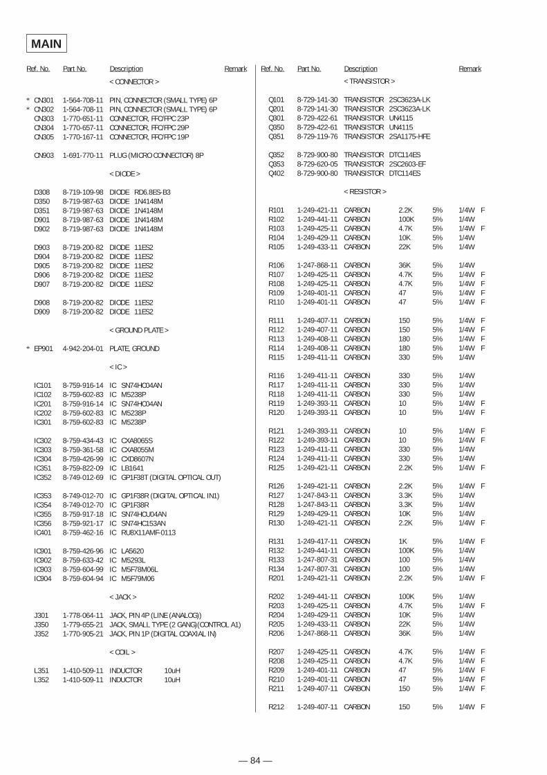
— 84 —
MAIN
Ref. No. Part No. Description Remark
< CONNECTOR >
* CN301 1-564-708-11 PIN, CONNECTOR (SMALL TYPE) 6P* CN302 1-564-708-11 PIN, CONNECTOR (SMALL TYPE) 6P
CN303 1-770-651-11 CONNECTOR, FFC/FPC 23PCN304 1-770-657-11 CONNECTOR, FFC/FPC 29PCN305 1-770-167-11 CONNECTOR, FFC/FPC 19P
CN903 1-691-770-11 PLUG (MICRO CONNECTOR) 8P
< DIODE >
D308 8-719-109-98 DIODE RD6.8ES-B3D350 8-719-987-63 DIODE 1N4148MD351 8-719-987-63 DIODE 1N4148MD901 8-719-987-63 DIODE 1N4148MD902 8-719-987-63 DIODE 1N4148M
D903 8-719-200-82 DIODE 11ES2D904 8-719-200-82 DIODE 11ES2D905 8-719-200-82 DIODE 11ES2D906 8-719-200-82 DIODE 11ES2D907 8-719-200-82 DIODE 11ES2
D908 8-719-200-82 DIODE 11ES2D909 8-719-200-82 DIODE 11ES2
< GROUND PLATE >
* EP901 4-942-204-01 PLATE, GROUND
< IC >
IC101 8-759-916-14 IC SN74HC04ANIC102 8-759-602-83 IC M5238PIC201 8-759-916-14 IC SN74HC04ANIC202 8-759-602-83 IC M5238PIC301 8-759-602-83 IC M5238P
IC302 8-759-434-43 IC CXA8065SIC303 8-759-361-58 IC CXA8055MIC304 8-759-426-99 IC CXD8607NIC351 8-759-822-09 IC LB1641IC352 8-749-012-69 IC GP1F38T (DIGITAL OPTICAL OUT)
IC353 8-749-012-70 IC GP1F38R (DIGITAL OPTICAL IN1)IC354 8-749-012-70 IC GP1F38RIC355 8-759-917-18 IC SN74HCU04ANIC356 8-759-921-17 IC SN74HC153ANIC401 8-759-462-16 IC RU8X11AMF-0113
IC901 8-759-426-96 IC LA5620IC902 8-759-633-42 IC M5293LIC903 8-759-604-99 IC M5F78M06LIC904 8-759-604-94 IC M5F79M06
< JACK >
J301 1-778-064-11 JACK, PIN 4P (LINE (ANALOG))J350 1-779-655-21 JACK, SMALL TYPE (2 GANG)(CONTROL A1)J352 1-770-905-21 JACK, PIN 1P (DIGITAL COAXIAL IN)
< COIL >
L351 1-410-509-11 INDUCTOR 10uHL352 1-410-509-11 INDUCTOR 10uH
Ref. No. Part No. Description Remark
< TRANSISTOR >
Q101 8-729-141-30 TRANSISTOR 2SC3623A-LKQ201 8-729-141-30 TRANSISTOR 2SC3623A-LKQ301 8-729-422-61 TRANSISTOR UN4115Q350 8-729-422-61 TRANSISTOR UN4115Q351 8-729-119-76 TRANSISTOR 2SA1175-HFE
Q352 8-729-900-80 TRANSISTOR DTC114ESQ353 8-729-620-05 TRANSISTOR 2SC2603-EFQ402 8-729-900-80 TRANSISTOR DTC114ES
< RESISTOR >
R101 1-249-421-11 CARBON 2.2K 5% 1/4W FR102 1-249-441-11 CARBON 100K 5% 1/4WR103 1-249-425-11 CARBON 4.7K 5% 1/4W FR104 1-249-429-11 CARBON 10K 5% 1/4WR105 1-249-433-11 CARBON 22K 5% 1/4W
R106 1-247-868-11 CARBON 36K 5% 1/4WR107 1-249-425-11 CARBON 4.7K 5% 1/4W FR108 1-249-425-11 CARBON 4.7K 5% 1/4W FR109 1-249-401-11 CARBON 47 5% 1/4W FR110 1-249-401-11 CARBON 47 5% 1/4W F
R111 1-249-407-11 CARBON 150 5% 1/4W FR112 1-249-407-11 CARBON 150 5% 1/4W FR113 1-249-408-11 CARBON 180 5% 1/4W FR114 1-249-408-11 CARBON 180 5% 1/4W FR115 1-249-411-11 CARBON 330 5% 1/4W
R116 1-249-411-11 CARBON 330 5% 1/4WR117 1-249-411-11 CARBON 330 5% 1/4WR118 1-249-411-11 CARBON 330 5% 1/4WR119 1-249-393-11 CARBON 10 5% 1/4W FR120 1-249-393-11 CARBON 10 5% 1/4W F
R121 1-249-393-11 CARBON 10 5% 1/4W FR122 1-249-393-11 CARBON 10 5% 1/4W FR123 1-249-411-11 CARBON 330 5% 1/4WR124 1-249-411-11 CARBON 330 5% 1/4WR125 1-249-421-11 CARBON 2.2K 5% 1/4W F
R126 1-249-421-11 CARBON 2.2K 5% 1/4W FR127 1-247-843-11 CARBON 3.3K 5% 1/4WR128 1-247-843-11 CARBON 3.3K 5% 1/4WR129 1-249-429-11 CARBON 10K 5% 1/4WR130 1-249-421-11 CARBON 2.2K 5% 1/4W F
R131 1-249-417-11 CARBON 1K 5% 1/4W FR132 1-249-441-11 CARBON 100K 5% 1/4WR133 1-247-807-31 CARBON 100 5% 1/4WR134 1-247-807-31 CARBON 100 5% 1/4WR201 1-249-421-11 CARBON 2.2K 5% 1/4W F
R202 1-249-441-11 CARBON 100K 5% 1/4WR203 1-249-425-11 CARBON 4.7K 5% 1/4W FR204 1-249-429-11 CARBON 10K 5% 1/4WR205 1-249-433-11 CARBON 22K 5% 1/4WR206 1-247-868-11 CARBON 36K 5% 1/4W
R207 1-249-425-11 CARBON 4.7K 5% 1/4W FR208 1-249-425-11 CARBON 4.7K 5% 1/4W FR209 1-249-401-11 CARBON 47 5% 1/4W FR210 1-249-401-11 CARBON 47 5% 1/4W FR211 1-249-407-11 CARBON 150 5% 1/4W F
R212 1-249-407-11 CARBON 150 5% 1/4W F
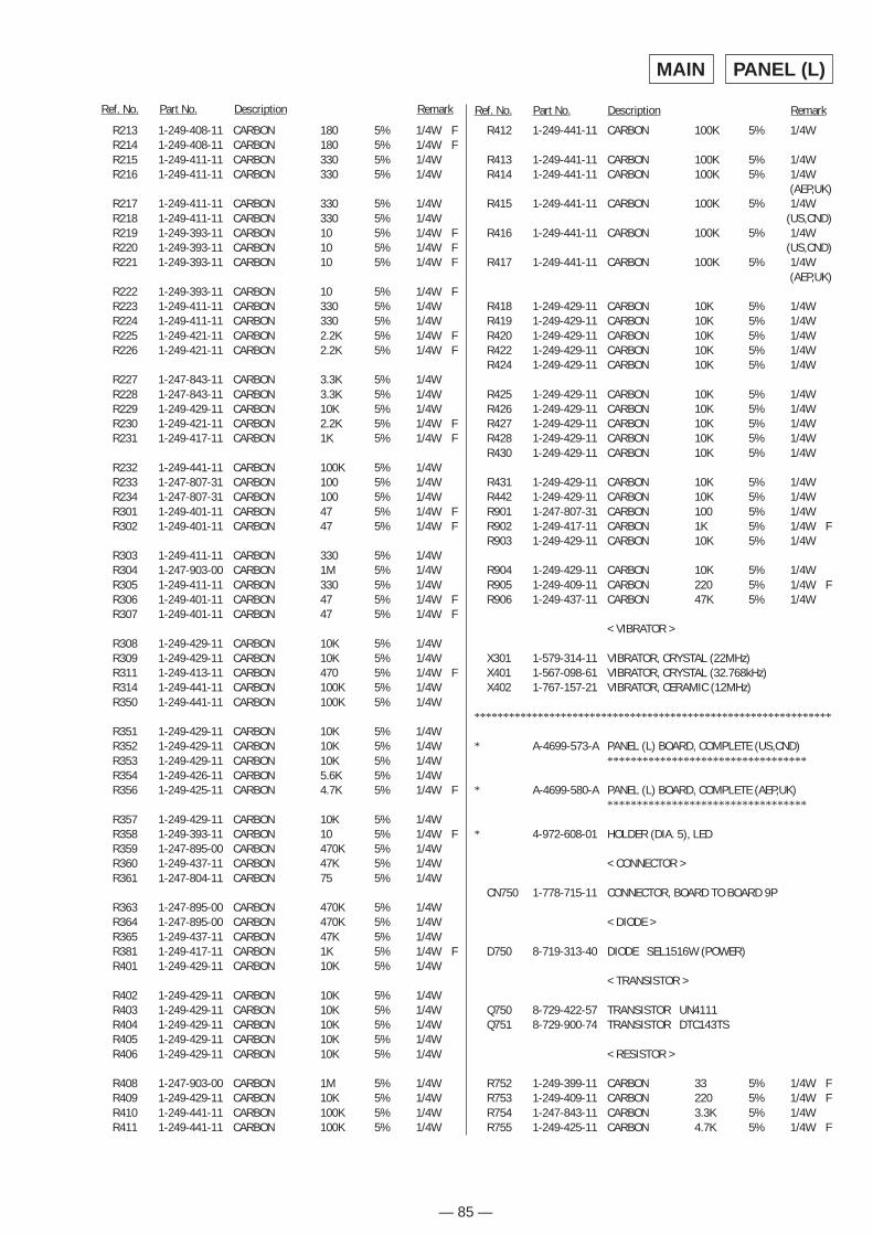
— 85 —
Ref. No. Part No. Description Remark
R213 1-249-408-11 CARBON 180 5% 1/4W FR214 1-249-408-11 CARBON 180 5% 1/4W FR215 1-249-411-11 CARBON 330 5% 1/4WR216 1-249-411-11 CARBON 330 5% 1/4W
R217 1-249-411-11 CARBON 330 5% 1/4WR218 1-249-411-11 CARBON 330 5% 1/4WR219 1-249-393-11 CARBON 10 5% 1/4W FR220 1-249-393-11 CARBON 10 5% 1/4W FR221 1-249-393-11 CARBON 10 5% 1/4W F
R222 1-249-393-11 CARBON 10 5% 1/4W FR223 1-249-411-11 CARBON 330 5% 1/4WR224 1-249-411-11 CARBON 330 5% 1/4WR225 1-249-421-11 CARBON 2.2K 5% 1/4W FR226 1-249-421-11 CARBON 2.2K 5% 1/4W F
R227 1-247-843-11 CARBON 3.3K 5% 1/4WR228 1-247-843-11 CARBON 3.3K 5% 1/4WR229 1-249-429-11 CARBON 10K 5% 1/4WR230 1-249-421-11 CARBON 2.2K 5% 1/4W FR231 1-249-417-11 CARBON 1K 5% 1/4W F
R232 1-249-441-11 CARBON 100K 5% 1/4WR233 1-247-807-31 CARBON 100 5% 1/4WR234 1-247-807-31 CARBON 100 5% 1/4WR301 1-249-401-11 CARBON 47 5% 1/4W FR302 1-249-401-11 CARBON 47 5% 1/4W F
R303 1-249-411-11 CARBON 330 5% 1/4WR304 1-247-903-00 CARBON 1M 5% 1/4WR305 1-249-411-11 CARBON 330 5% 1/4WR306 1-249-401-11 CARBON 47 5% 1/4W FR307 1-249-401-11 CARBON 47 5% 1/4W F
R308 1-249-429-11 CARBON 10K 5% 1/4WR309 1-249-429-11 CARBON 10K 5% 1/4WR311 1-249-413-11 CARBON 470 5% 1/4W FR314 1-249-441-11 CARBON 100K 5% 1/4WR350 1-249-441-11 CARBON 100K 5% 1/4W
R351 1-249-429-11 CARBON 10K 5% 1/4WR352 1-249-429-11 CARBON 10K 5% 1/4WR353 1-249-429-11 CARBON 10K 5% 1/4WR354 1-249-426-11 CARBON 5.6K 5% 1/4WR356 1-249-425-11 CARBON 4.7K 5% 1/4W F
R357 1-249-429-11 CARBON 10K 5% 1/4WR358 1-249-393-11 CARBON 10 5% 1/4W FR359 1-247-895-00 CARBON 470K 5% 1/4WR360 1-249-437-11 CARBON 47K 5% 1/4WR361 1-247-804-11 CARBON 75 5% 1/4W
R363 1-247-895-00 CARBON 470K 5% 1/4WR364 1-247-895-00 CARBON 470K 5% 1/4WR365 1-249-437-11 CARBON 47K 5% 1/4WR381 1-249-417-11 CARBON 1K 5% 1/4W FR401 1-249-429-11 CARBON 10K 5% 1/4W
R402 1-249-429-11 CARBON 10K 5% 1/4WR403 1-249-429-11 CARBON 10K 5% 1/4WR404 1-249-429-11 CARBON 10K 5% 1/4WR405 1-249-429-11 CARBON 10K 5% 1/4WR406 1-249-429-11 CARBON 10K 5% 1/4W
R408 1-247-903-00 CARBON 1M 5% 1/4WR409 1-249-429-11 CARBON 10K 5% 1/4WR410 1-249-441-11 CARBON 100K 5% 1/4WR411 1-249-441-11 CARBON 100K 5% 1/4W
Ref. No. Part No. Description Remark
R412 1-249-441-11 CARBON 100K 5% 1/4W
R413 1-249-441-11 CARBON 100K 5% 1/4WR414 1-249-441-11 CARBON 100K 5% 1/4W
(AEP,UK)R415 1-249-441-11 CARBON 100K 5% 1/4W
(US,CND)R416 1-249-441-11 CARBON 100K 5% 1/4W
(US,CND)R417 1-249-441-11 CARBON 100K 5% 1/4W
(AEP,UK)
R418 1-249-429-11 CARBON 10K 5% 1/4WR419 1-249-429-11 CARBON 10K 5% 1/4WR420 1-249-429-11 CARBON 10K 5% 1/4WR422 1-249-429-11 CARBON 10K 5% 1/4WR424 1-249-429-11 CARBON 10K 5% 1/4W
R425 1-249-429-11 CARBON 10K 5% 1/4WR426 1-249-429-11 CARBON 10K 5% 1/4WR427 1-249-429-11 CARBON 10K 5% 1/4WR428 1-249-429-11 CARBON 10K 5% 1/4WR430 1-249-429-11 CARBON 10K 5% 1/4W
R431 1-249-429-11 CARBON 10K 5% 1/4WR442 1-249-429-11 CARBON 10K 5% 1/4WR901 1-247-807-31 CARBON 100 5% 1/4WR902 1-249-417-11 CARBON 1K 5% 1/4W FR903 1-249-429-11 CARBON 10K 5% 1/4W
R904 1-249-429-11 CARBON 10K 5% 1/4WR905 1-249-409-11 CARBON 220 5% 1/4W FR906 1-249-437-11 CARBON 47K 5% 1/4W
< VIBRATOR >
X301 1-579-314-11 VIBRATOR, CRYSTAL (22MHz)X401 1-567-098-61 VIBRATOR, CRYSTAL (32.768kHz)X402 1-767-157-21 VIBRATOR, CERAMIC (12MHz)
**************************************************************
* A-4699-573-A PANEL (L) BOARD, COMPLETE (US,CND)**********************************
* A-4699-580-A PANEL (L) BOARD, COMPLETE (AEP,UK)**********************************
* 4-972-608-01 HOLDER (DIA. 5), LED
< CONNECTOR >
CN750 1-778-715-11 CONNECTOR, BOARD TO BOARD 9P
< DIODE >
D750 8-719-313-40 DIODE SEL1516W (POWER)
< TRANSISTOR >
Q750 8-729-422-57 TRANSISTOR UN4111Q751 8-729-900-74 TRANSISTOR DTC143TS
< RESISTOR >
R752 1-249-399-11 CARBON 33 5% 1/4W FR753 1-249-409-11 CARBON 220 5% 1/4W FR754 1-247-843-11 CARBON 3.3K 5% 1/4WR755 1-249-425-11 CARBON 4.7K 5% 1/4W F
PANEL (L)MAIN
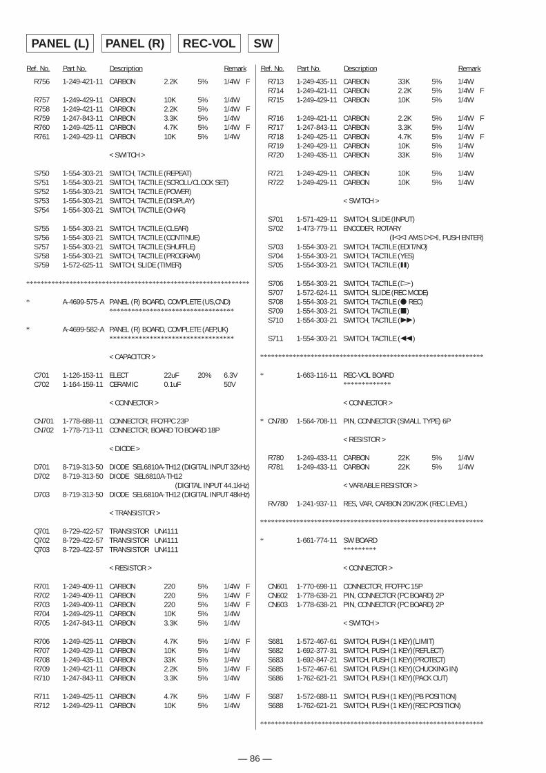
— 86 —
Ref. No. Part No. Description Remark
R756 1-249-421-11 CARBON 2.2K 5% 1/4W F
R757 1-249-429-11 CARBON 10K 5% 1/4WR758 1-249-421-11 CARBON 2.2K 5% 1/4W FR759 1-247-843-11 CARBON 3.3K 5% 1/4WR760 1-249-425-11 CARBON 4.7K 5% 1/4W FR761 1-249-429-11 CARBON 10K 5% 1/4W
< SWITCH >
S750 1-554-303-21 SWITCH, TACTILE (REPEAT)S751 1-554-303-21 SWITCH, TACTILE (SCROLL/CLOCK SET)S752 1-554-303-21 SWITCH, TACTILE (POWER)S753 1-554-303-21 SWITCH, TACTILE (DISPLAY)S754 1-554-303-21 SWITCH, TACTILE (CHAR)
S755 1-554-303-21 SWITCH, TACTILE (CLEAR)S756 1-554-303-21 SWITCH, TACTILE (CONTINUE)S757 1-554-303-21 SWITCH, TACTILE (SHUFFLE)S758 1-554-303-21 SWITCH, TACTILE (PROGRAM)S759 1-572-625-11 SWITCH, SLIDE (TIMER)
**************************************************************
* A-4699-575-A PANEL (R) BOARD, COMPLETE (US,CND)**********************************
* A-4699-582-A PANEL (R) BOARD, COMPLETE (AEP,UK)**********************************
< CAPACITOR >
C701 1-126-153-11 ELECT 22uF 20% 6.3VC702 1-164-159-11 CERAMIC 0.1uF 50V
< CONNECTOR >
CN701 1-778-688-11 CONNECTOR, FFC/FPC 23PCN702 1-778-713-11 CONNECTOR, BOARD TO BOARD 18P
< DIODE >
D701 8-719-313-50 DIODE SEL6810A-TH12 (DIGITAL INPUT 32kHz)D702 8-719-313-50 DIODE SEL6810A-TH12
(DIGITAL INPUT 44.1kHz)D703 8-719-313-50 DIODE SEL6810A-TH12 (DIGITAL INPUT 48kHz)
< TRANSISTOR >
Q701 8-729-422-57 TRANSISTOR UN4111Q702 8-729-422-57 TRANSISTOR UN4111Q703 8-729-422-57 TRANSISTOR UN4111
< RESISTOR >
R701 1-249-409-11 CARBON 220 5% 1/4W FR702 1-249-409-11 CARBON 220 5% 1/4W FR703 1-249-409-11 CARBON 220 5% 1/4W FR704 1-249-429-11 CARBON 10K 5% 1/4WR705 1-247-843-11 CARBON 3.3K 5% 1/4W
R706 1-249-425-11 CARBON 4.7K 5% 1/4W FR707 1-249-429-11 CARBON 10K 5% 1/4WR708 1-249-435-11 CARBON 33K 5% 1/4WR709 1-249-421-11 CARBON 2.2K 5% 1/4W FR710 1-247-843-11 CARBON 3.3K 5% 1/4W
R711 1-249-425-11 CARBON 4.7K 5% 1/4W FR712 1-249-429-11 CARBON 10K 5% 1/4W
Ref. No. Part No. Description Remark
PANEL (L) PANEL (R) REC-VOL SW
R713 1-249-435-11 CARBON 33K 5% 1/4WR714 1-249-421-11 CARBON 2.2K 5% 1/4W FR715 1-249-429-11 CARBON 10K 5% 1/4W
R716 1-249-421-11 CARBON 2.2K 5% 1/4W FR717 1-247-843-11 CARBON 3.3K 5% 1/4WR718 1-249-425-11 CARBON 4.7K 5% 1/4W FR719 1-249-429-11 CARBON 10K 5% 1/4WR720 1-249-435-11 CARBON 33K 5% 1/4W
R721 1-249-429-11 CARBON 10K 5% 1/4WR722 1-249-429-11 CARBON 10K 5% 1/4W
< SWITCH >
S701 1-571-429-11 SWITCH, SLIDE (INPUT)S702 1-473-779-11 ENCODER, ROTARY
(≠ AMS ±, PUSH ENTER)S703 1-554-303-21 SWITCH, TACTILE (EDIT/NO)S704 1-554-303-21 SWITCH, TACTILE (YES)S705 1-554-303-21 SWITCH, TACTILE (P)
S706 1-554-303-21 SWITCH, TACTILE (·)S707 1-572-624-11 SWITCH, SLIDE (REC MODE)S708 1-554-303-21 SWITCH, TACTILE (r REC)S709 1-554-303-21 SWITCH, TACTILE (p)S710 1-554-303-21 SWITCH, TACTILE ())
S711 1-554-303-21 SWITCH, TACTILE (0)
**************************************************************
* 1-663-116-11 REC-VOL BOARD*************
< CONNECTOR >
* CN780 1-564-708-11 PIN, CONNECTOR (SMALL TYPE) 6P
< RESISTOR >
R780 1-249-433-11 CARBON 22K 5% 1/4WR781 1-249-433-11 CARBON 22K 5% 1/4W
< VARIABLE RESISTOR >
RV780 1-241-937-11 RES, VAR, CARBON 20K/20K (REC LEVEL)
**************************************************************
* 1-661-774-11 SW BOARD*********
< CONNECTOR >
CN601 1-770-698-11 CONNECTOR, FFC/FPC 15PCN602 1-778-638-21 PIN, CONNECTOR (PC BOARD) 2PCN603 1-778-638-21 PIN, CONNECTOR (PC BOARD) 2P
< SWITCH >
S681 1-572-467-61 SWITCH, PUSH (1 KEY)(LIMIT)S682 1-692-377-31 SWITCH, PUSH (1 KEY)(REFLECT)S683 1-692-847-21 SWITCH, PUSH (1 KEY)(PROTECT)S685 1-572-467-61 SWITCH, PUSH (1 KEY)(CHUCKING IN)S686 1-762-621-21 SWITCH, PUSH (1 KEY)(PACK OUT)
S687 1-572-688-11 SWITCH, PUSH (1 KEY)(PB POSITION)S688 1-762-621-21 SWITCH, PUSH (1 KEY)(REC POSITION)
**************************************************************
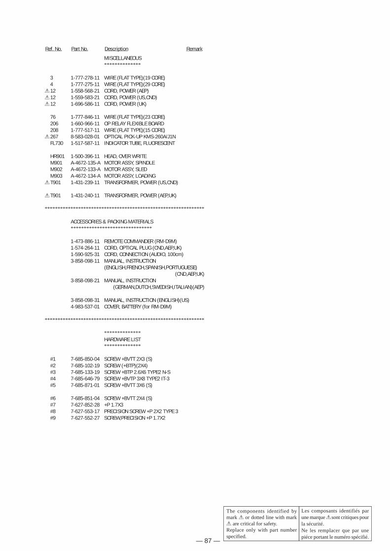
— 87 —
Ref. No. Part No. Description Remark
MISCELLANEOUS**************
3 1-777-278-11 WIRE (FLAT TYPE)(19 CORE)4 1-777-275-11 WIRE (FLAT TYPE)(29 CORE)!12 1-558-568-21 CORD, POWER (AEP)!12 1-559-583-21 CORD, POWER (US,CND)!12 1-696-586-11 CORD, POWER (UK)
76 1-777-846-11 WIRE (FLAT TYPE)(23 CORE)206 1-660-966-11 OP RELAY FLEXIBLE BOARD208 1-777-517-11 WIRE (FLAT TYPE)(15 CORE)!267 8-583-028-01 OPTICAL PICK-UP KMS-260A/J1N
FL730 1-517-587-11 INDICATOR TUBE, FLUORESCENT
HR901 1-500-396-11 HEAD, OVER WRITEM901 A-4672-135-A MOTOR ASSY, SPINDLEM902 A-4672-133-A MOTOR ASSY, SLEDM903 A-4672-134-A MOTOR ASSY, LOADING!T901 1-431-239-11 TRANSFORMER, POWER (US,CND)
!T901 1-431-240-11 TRANSFORMER, POWER (AEP,UK)
**************************************************************
ACCESSORIES & PACKING MATERIALS*******************************
1-473-886-11 REMOTE COMMANDER (RM-D9M)1-574-264-11 CORD, OPTICAL PLUG (CND,AEP,UK)1-590-925-31 CORD, CONNECTION (AUDIO, 100cm)3-858-098-11 MANUAL, INSTRUCTION
(ENGLISH,FRENCH,SPANISH,PORTUGUESE)(CND,AEP,UK)
3-858-098-21 MANUAL, INSTRUCTION(GERMAN,DUTCH,SWEDISH,ITALIAN)(AEP)
3-858-098-31 MANUAL, INSTRUCTION (ENGLISH)(US)4-983-537-01 COVER, BATTERY (for RM-D9M)
**************************************************************
**************HARDWARE LIST**************
#1 7-685-850-04 SCREW +BVTT 2X3 (S)#2 7-685-102-19 SCREW (+BTP)(2X4)#3 7-685-133-19 SCREW +BTP 2.6X6 TYPE2 N-S#4 7-685-646-79 SCREW +BVTP 3X8 TYPE2 IT-3#5 7-685-871-01 SCREW +BVTT 3X6 (S)
#6 7-685-851-04 SCREW +BVTT 2X4 (S)#7 7-627-852-28 +P 1.7X3#8 7-627-553-17 PRECISION SCREW +P 2X2 TYPE 3#9 7-627-552-27 SCREW,PRECISION +P 1.7X2
Les composants identifiés parune marque ! sont critiques pourla sécurité.Ne les remplacer que par unepiéce portant le numéro spécifié.
The components identified bymark ! or dotted line with mark! are critical for safety.Replace only with part numberspecified.

— 88 —
MDS-JE700
9-960-804-11Sony Corporation
Home A&V Products Company97B0977-1
Printed in Japan © 1997. 2Published by Service and Safety
Engineering Dept. (Shibaura)