mcp9800/1/2/3, 2-wire high-accuracy temperature sensor...
TRANSCRIPT

MCP9800/1/2/32-Wire High-Accuracy Temperature Sensor
Features:• Temperature-to-Digital Converter• Accuracy with 12-bit Resolution:
- ±0.5°C (typical) at +25°C- ±1°C (maximum) from -10°C to +85°C- ±2°C (maximum) from -10°C to +125°C- ±3°C (maximum) from -55°C to +125°C
• User-selectable Resolution: 9-12 bit• Operating Voltage Range: 2.7V to 5.5V• 2-wire Interface: I2C™/SMBus Compatible• Operating Current: 200 µA (typical)• Shutdown Current: 1 µA (maximum)• Power-saving One-shot Temperature
Measurement• Available Packages: SOT-23-5, MSOP-8, SOIC-8
Typical Applications:• Personal Computers and Servers• Hard Disk Drives and Other PC Peripherals• Entertainment Systems• Office Equipment• Data Communication Equipment• Mobile Phones• General Purpose Temperature Monitoring
Typical Application
Description:Microchip Technology Inc.’s MCP9800/1/2/3 family ofdigital temperature sensors converts temperaturesbetween -55°C and +125°C to a digital word. Theyprovide an accuracy of ±1°C (maximum) from -10°C to+85°C.
The MCP9800/1/2/3 family comes withuser-programmable registers that provide flexibility fortemperature sensing applications. The register settingsallow user-selectable 9-bit to 12-bit temperaturemeasurement resolution, configuration of thepower-saving Shutdown and One-shot (singleconversion on command while in Shutdown) modesand the specification of both temperature alert outputand hysteresis limits. When the temperature changesbeyond the specified limits, the MCP9800/1/2/3 outputsan alert signal. The user has the option of setting thealert output signal polarity as an active-low oractive-high comparator output for thermostat operation,or as temperature event interrupt output formicroprocessor-based systems.
This sensor has an industry standard 2-wire, I2C™/SMBus compatible serial interface, allowing up to eightdevices to be controlled in a single serial bus. Thesefeatures make the MCP9800/1/2/3 ideal forsophisticated multi-zone temperature-monitoringapplications.
Package Types
PIC®VDD
RMicrocontroller
MCP9800/02
GND
VDD
ALERT
SDA
SCLK4
123
5 I 2C™
Port I/O Port
RPULL-UP
PIC16F737 SDA
GNDALERT
SCLKGND
VDD
ALERT
SDA
SCLK4
MCP9800MCP9802
1
2
3
5
SOT-23-5
MCP9801MCP9803
1
2
3
4
8
7
6
5
SOIC, MSOP
A0
VDD
A1A2
MCP9802/03: Serial Bus time-out 35 ms (typ.)MCP9800/01: No Serial Bus time-out
2010 Microchip Technology Inc. DS21909D-page 1

MCP9800/1/2/3
NOTES:DS21909D-page 2 2010 Microchip Technology Inc.

MCP9800/1/2/3
1.0 ELECTRICAL CHARACTERISTICS
Absolute Maximum Ratings †VDD....................................................................... 6.0V
Voltage at all Input/Output pins .....GND – 0.3V to 5.5V
Storage temperature .......................... -65°C to +150°C
Ambient temp. with power applied ..... -55°C to +125°C
Junction Temperature (TJ) ................................. 150°C
ESD protection on all pins (HBM:MM) .......(4 kV:400V)
Latch-Up Current at each pin ........................ ±200 mA
†Notice: Stresses above those listed under “Maximumratings” may cause permanent damage to the device. This isa stress rating only and functional operation of the device atthose or any other conditions above those indicated in theoperational listings of this specification is not implied.Exposure to maximum rating conditions for extended periodsmay affect device reliability.
DC CHARACTERISTICSElectrical Specifications: Unless otherwise indicated, VDD = 2.7V to 5.5V, GND = Ground, andTA = -55°C to +125°C.
Parameters Sym Min Typ Max Unit Conditions
Power Supply Operating Voltage Range VDD 2.7 — 5.5 VOperating Current IDD — 200 400 µA Continuous OperationShutdown Current ISHDN — 0.1 1 µA Shutdown mode
Power-on-Reset Threshold (POR) VPOR — 1.7 — V VDD falling edge
Line Regulation Δ°C/ΔV — 0.2 — °C/V VDD = 2.7V to 5.5VTemperature Sensor AccuracyAccuracy with 12-bit Resolution:
TA = +25°C TACY — ±0.5 — °C VDD = 3.3V-10°C < TA +85°C TACY -1.0 — +1.0 °C VDD = 3.3V-10°C < TA +125°C TACY -2.0 — +2.0 °C VDD = 3.3V-55°C < TA +125°C TACY -3.0 — +3.0 °C VDD = 3.3V
Internal ADCConversion Time:
9-bit Resolution tCONV — 30 75 ms 33 samples/sec (typical)10-bit Resolution tCONV — 60 150 ms 17 samples/sec (typical)11-bit Resolution tCONV — 120 300 ms 8 samples/sec (typical)12-bit Resolution tCONV — 240 600 ms 4 samples/sec (typical)
Alert Output (Open-drain)High-level Current IOH — — 1 µA VOH = 5V
Low-level Voltage VOL — — 0.4 V IOL= 3 mA
Thermal ResponseResponse Time tRES — 1.4 — s Time to 63% (89°C)
27°C (Air) to 125°C (oil bath)
2010 Microchip Technology Inc. DS21909D-page 3

MCP9800/1/2/3
Graphical Symbol Description
DIGITAL INPUT/OUTPUT PIN CHARACTERISTICSElectrical Specifications: Unless otherwise indicated, VDD = 2.7V to 5.5V, GND = Ground andTA = -55°C to +125°C.
Parameters Sym Min Typ Max Units Conditions
Serial Input/Output (SCLK, SDA, A0, A1, A2)Input
High-level Voltage VIH 0.7 VDD — — VLow-level Voltage VIL — — 0.3 VDD VInput Current IIN -1 — +1 µA
Output (SDA)Low-level Voltage VOL — — 0.4 V IOL= 3 mAHigh-level Current IOH — — 1 µA VOH = 5VLow-level Current IOL 6 — — mA VOL = 0.6V
Capacitance CIN — 10 — pFSDA and SCLK InputsHysteresis VHYST 0.05 VDD — — V
TEMPERATURE CHARACTERISTICSElectrical Specifications: Unless otherwise indicated, VDD = +2.7V to +5.5V, GND = Ground.
Parameters Sym Min Typ Max Units ConditionsTemperature RangesSpecified Temperature Range TA -55 — +125 °C (Note 1)Operating Temperature Range TA -55 — +125 °CStorage Temperature Range TA -65 — +150 °CThermal Package ResistancesThermal Resistance, 5L-SOT23 JA — 256 — °C/WThermal Resistance, 8L-SOIC JA — 163 — °C/WThermal Resistance, 8L-MSOP JA — 206 — °C/WNote 1: Operation in this range must not cause TJ to exceed Maximum Junction Temperature (+150°C).
VDD VIH
VIL
IIN
Voltage
CurrentTime
Time
VDD
IOH
Voltage
CurrentTime
Time
INPUT OUTPUT
VOL
IOL
DS21909D-page 4 2010 Microchip Technology Inc.

MCP9800/1/2/3
Timing Diagram
SERIAL INTERFACE TIMING SPECIFICATIONSElectrical Specifications: Unless otherwise indicated, VDD = 2.7V to 5.5V, GND = Ground, -55°C < TA < +125°C, CL = 80 pF, and all limits measured to 50% point.
Parameters Sym Min Typ Max Units Conditions
2-Wire I2C™/SMBus Compatible Interface Serial Port Frequency fSC 0 — 400 kHz I2C MCP9800/01
fSC 10 — 400 kHz SMBus MCP9802/03Clock Period tSC 2.5 — — µs
Low Clock tLOW 1.3 — — µs
High Clock tHIGH 0.6 — — µs
Rise Time tR 20 — 300 ns 10% to 90% of VDD (SCLK, SDA)
Fall Time tF 20 — 300 ns 90% to 10% of VDD (SCLK, SDA)
Data Setup Before SCLK High tSU-DATA 0.1 — — µs
Data Hold After SCLK Low tH-DATA 0 — 0.9 µs
Start Condition Setup Time tSU-START 0.6 — — µs
Start Condition Hold Time tH-START 0.6 — — µs
Stop Condition Setup Time tSU-STOP 0.6 — — µs
Bus Idle tIDLE 1.3 — — µs
Time Out tOUT 25 35 50 ms MCP9802/03 only
t SU-STA
RT
t H-STA
RT
t SU-DATA
t SU-STOP
t B-FREE
SCL
SDA
t H-DATA
t HIGH
t LOW
t R, t F
Start Condition Data Transmission Stop Condition
2010 Microchip Technology Inc. DS21909D-page 5

MCP9800/1/2/3
NOTES:DS21909D-page 6 2010 Microchip Technology Inc.

MCP9800/1/2/3
2.0 TYPICAL PERFORMANCE CURVES
Note: Unless otherwise noted: VDD = 2.7V to 5.5V.
FIGURE 2-1: Average Temperature Accuracy vs. Ambient Temperature, VDD = 3.3V.
FIGURE 2-2: Average Temperature Accuracy vs. Ambient Temperature.
FIGURE 2-3: Average Temperature Accuracy vs. Ambient Temperature, VDD = 3.3V.
FIGURE 2-4: Temperature Accuracy Histogram, TA = +25°C.
FIGURE 2-5: Supply Current vs. Ambient Temperature.
FIGURE 2-6: Shutdown Current vs. Ambient Temperature.
Note: The graphs and tables provided following this note are a statistical summary based on a limited number ofsamples and are provided for informational purposes only. The performance characteristics listed hereinare not tested or guaranteed. In some graphs or tables, the data presented may be outside the specifiedoperating range (e.g., outside specified power supply range) and therefore, outside the warranted range.
-3.0
-2.0
-1.0
0.0
1.0
2.0
3.0
-55 -35 -15 5 25 45 65 85 105 125TA (°C)
Tem
pera
ture
Acc
urac
y (°
C)
12-Bit Resolution160 Samples
VDD= 3.3V
Spec. Limits
-3.0
-2.0
-1.0
0.0
1.0
2.0
3.0
-55 -35 -15 5 25 45 65 85 105 125TA (°C)
Tem
pera
ture
Acc
urac
y (°
C) 12-Bit Resolution
160 SamplesVDD = 2.7VVDD = 3.3V
VDD = 5.5VVDD = 5.0V
-3.0
-2.0
-1.0
0.0
1.0
2.0
3.0
-55 -35 -15 5 25 45 65 85 105 125TA (°C)
Tem
pera
ture
Acc
urac
y (°
C)
11-Bit12-Bit
9-Bit10-Bit
VDD = 3.3V160 Samples
Resolution
0%10%20%30%40%50%60%70%80%90%
100%
-3.0
-2.5
-2.0
-1.5
-1.0
-0.5 0.0
0.5
1.0
1.5
2.0
2.5
3.0
Temperature Accuracy (°C)
Occ
urre
nces
TA = +25°CVDD = 3.3V
5 lots32 Samples/lot160 Samples
50
100
150
200
250
300
350
400
-55 -35 -15 5 25 45 65 85 105 125TA (°C)
I DD (µ
A)
VDD = 2.7VVDD = 3.3V
VDD = 5.5VVDD = 5.0V
0
0.2
0.4
0.6
0.8
1
-55 -35 -15 5 25 45 65 85 105 125TA (°C )
I SH
DN (µ
A)
2010 Microchip Technology Inc. DS21909D-page 7

MCP9800/1/2/3
Note: Unless otherwise noted: VDD = 2.7V to 5.5V.FIGURE 2-7: ALERT and SDA IOL vs. Ambient Temperature.
FIGURE 2-8: ALERT and SDA Output VOL vs. Ambient Temperature.
FIGURE 2-9: MCP980X Thermal Response vs Time.
6
12
18
24
30
36
42
48
-55 -35 -15 5 25 45 65 85 105 125TA (°C)
ALE
RT
& S
DA
I OL (
mA
)
VDD = 5.5VVDD = 3.3VVDD = 2.7V
VOL = 0.6V
0
0.1
0.2
0.3
0.4
-55 -35 -15 5 25 45 65 85 105 125TA (°C)
ALE
RT
& S
DA
VO
L (V)
VDD = 5.5VVDD = 3.3VVDD = 2.7V
IOL = 3mA
5
25
45
65
85
105
125
145
-2 0 2 4 6 8 10 12 14 16 18 20Time (s)
Tem
pera
ture
Dat
a (°
C)
SOIC
Average of 10 samples per package
27°C (Air) to 125°C (Oil bath)
MSOP
SOT-23
DS21909D-page 8 2010 Microchip Technology Inc.

MCP9800/1/2/3
3.0 PIN DESCRIPTIONThe descriptions of the pins are listed in Table 3-1.
TABLE 3-1: PIN FUNCTION TABLE
3.1 Serial Data Pin (SDA) The SDA is a bidirectional input/output pin, used toserially transmit data to and from the host controller.This pin requires a pull-up resistor to output data.
3.2 Serial Clock Pin (SCLK)The SCLK is a clock input pin. All communication andtiming is relative to the signal on this pin. The clock isgenerated by the host controller on the bus.
3.3 Power Supply Input (VDD)The VDD pin is the power pin. The operating voltage, asspecified in the DC electrical specification table, isapplied on this pin.
3.4 Ground (GND)The GND pin is the system ground pin.
3.5 ALERT OutputThe MCP9800/1/2/3’s ALERT pin is an open-drainoutput pin. The device outputs an alert signal when theambient temperature goes beyond theuser-programmed temperature limit.
3.6 Address Pins (A2, A1, A0)These pins are device or slave address input pins andare available only with the MCP9801/03. The deviceaddresses for the MCP9800/02 are factory-set.
The address pins are the Least Significant bits (LSb) ofthe device address bits. The Most Significant bits(MSb) (A6, A5, A4, A3) are factory-set to <1001>. Thisis illustrated in Table 3-2.
MCP9800MCP9802SOT-23-5
MCP9801MCP9803
MSOP, SOICSymbol Function
5 1 SDA Bidirectional Serial Data4 2 SCLK Serial Clock Input3 3 ALERT Temperature Alert Output2 4 GND Ground— 5 A2 Address Select Pin (bit 2)— 6 A1 Address Select Pin (bit 1)— 7 A0 Address Select Pin (bit 0)1 8 VDD Power Supply Input
TABLE 3-2: SLAVE ADDRESSDevice A6 A5 A4 A3 A2 A1 A0
MCP9800/02A0 1 0 0 1 0 0 0MCP9800/02A1 1 0 0 1 0 0 1MCP9800/02A2 1 0 0 1 0 1 0MCP9800/02A3 1 0 0 1 0 1 1MCP9800/02A4 1 0 0 1 1 0 0MCP9800/02A5 1 0 0 1 1 0 1MCP9800/02A6 1 0 0 1 1 1 0MCP9800/02A7 1 0 0 1 1 1 1MCP9801/03 1 0 0 1 X X X
Note: User-selectable address is shown by X.
2010 Microchip Technology Inc. DS21909D-page 9

MCP9800/1/2/3
NOTES:DS21909D-page 10 2010 Microchip Technology Inc.

MCP9800/1/2/3
4.0 SERIAL COMMUNICATION
4.1 2-Wire SMBus/Standard Mode I2C™ Protocol-Compatible Interface
The MCP9800/1/2/3 serial clock input (SCL) and thebidirectional serial data line (SDA) form a 2-wirebidirectional SMBus/Standard mode I2C compatiblecommunication port (refer to the Digital Input/OutputPin Characteristics Table and Serial InterfaceTiming Specifications Table).
The following bus protocol has been defined:
TABLE 4-1: MCP9800 SERIAL BUS PROTOCOL DESCRIPTIONS
4.1.1 DATA TRANSFERData transfers are initiated by a Start condition (Start),followed by a 7-bit device address and a read/write bit.An Acknowledge (ACK) from the slave confirms thereception of each byte. Each access must beterminated by a Stop condition (Stop).
Repeated communication is initiated after tB-FREE.
This device does not support sequential register read/write. Each register needs to be addressed using theRegister Pointer.
This device supports the Receive Protocol. Theregister can be specified using the pointer for the initialread. Each repeated read or receive begins with a Startcondition and address byte. The MCP9800/1/2/3retains the previously selected register. Therefore, itoutputs data from the previously-specified register(repeated pointer specification is not necessary).
4.1.2 MASTER/SLAVEThe bus is controlled by a master device (typically amicrocontroller) that controls the bus access andgenerates the Start and Stop conditions. TheMCP9800/1/2/3 is a slave device and does not controlother devices in the bus. Both master and slavedevices can operate as either transmitter or receiver.However, the master device determines which mode isactivated.
4.1.3 START/STOP CONDITION A high-to-low transition of the SDA line (while SCL ishigh) is the Start condition. All data transfers must bepreceded by a Start condition from the master. If a Startcondition is generated during data transfer, theMCP9800/1/2/3 resets and accepts the new Startcondition.
A low-to-high transition of the SDA line (while SCL ishigh) signifies a Stop condition. If a Stop condition isintroduced during data transmission, the MCP9800/1/2/3 releases the bus. All data transfers are ended by aStop condition from the master.
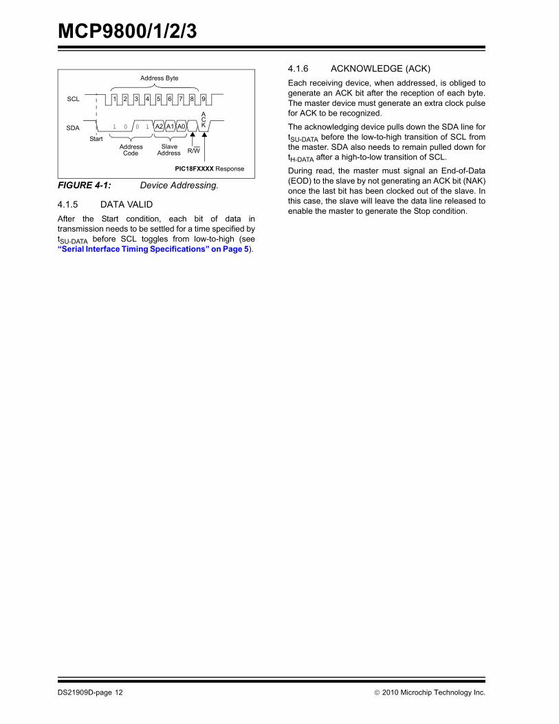
4.1.4 ADDRESS BYTEFollowing the Start condition, the host must transmit an8-bit address byte to the MCP9800/1/2/3. The addressfor the MCP9800 Temperature Sensor is‘1001,A2,A1,A0’ in binary, where the A2, A1 and A0bits are set externally by connecting the correspondingpins to VDD ‘1’ or GND ‘0’. The 7-bit addresstransmitted in the serial bit stream must match theselected address for the MCP9800/1/2/3 to respondwith an ACK. Bit 8 in the address byte is a read/writebit. Setting this bit to ‘1’ commands a read operation,while ‘0’ commands a write operation (see Figure 4-1).
Term Description
Master The device that controls the serial bus, typically a microcontroller.
Slave The device addressed by the master, such as the MCP9800/1/2/3.
Transmitter Device sending data to the bus.Receiver Device receiving data from the bus.Start A unique signal from master to initiate
serial interface with a slave.Stop A unique signal from the master to
terminate serial interface from a slave.Read/Write A read or write to the MCP9800/1/2/3
registers.ACK A receiver Acknowledges (ACK) the
reception of each byte by polling the bus.
NAK A receiver Not-Acknowledges (NAK) or releases the bus to show End-of-Data (EOD).
Busy Communication is not possible because the bus is in use.
Not Busy The bus is in the Idle state, both SDA and SCL remain high.
Data Valid SDA must remain stable before SCL becomes high in order for a data bit to be considered valid. During normal data transfers, SDA only changes state while SCL is low.
2010 Microchip Technology Inc. DS21909D-page 11
MCP9800/1/2/3
FIGURE 4-1: Device Addressing.
4.1.5 DATA VALID After the Start condition, each bit of data intransmission needs to be settled for a time specified bytSU-DATA before SCL toggles from low-to-high (see“Serial Interface Timing Specifications” on Page 5).
4.1.6 ACKNOWLEDGE (ACK)Each receiving device, when addressed, is obliged togenerate an ACK bit after the reception of each byte.The master device must generate an extra clock pulsefor ACK to be recognized.
The acknowledging device pulls down the SDA line fortSU-DATA before the low-to-high transition of SCL fromthe master. SDA also needs to remain pulled down fortH-DATA after a high-to-low transition of SCL.
During read, the master must signal an End-of-Data(EOD) to the slave by not generating an ACK bit (NAK)once the last bit has been clocked out of the slave. Inthis case, the slave will leave the data line released toenable the master to generate the Stop condition.
1 2 3 4 5 6 7 8 9SCL
SDA 1 0 0 1 A2 A1 A0
Start
Address Byte
SlaveAddress R/W
PIC18FXXXX Response
Code Address
ACK
DS21909D-page 12 2010 Microchip Technology Inc.

MCP9800/1/2/3
5.0 FUNCTIONAL DESCRIPTIONThe MCP9800/1/2/3 temperature sensor consists of aband-gap type temperature sensor, a Analog-to-Digital Converter (ADC), user-programmable registersand a 2-wire I2C protocol-compatible serial interface.
FIGURE 5-1: Functional Block Diagram.
5.1 Temperature SensorThe MCP9800/1/2/3 uses the difference in the base-emitter voltage of a transistor while its collector currentis changed from IC1 to IC2. With this method, the VBEdepends only on the ratio of the two currents and theambient temperature, as shown in Equation 5-1.
EQUATION 5-1:
5.2 Analog-to-Digital ConverterA Sigma-Delta ADC is used to convert VBE to a digitalword that corresponds to the transistor temperature.The converter has an adjustable resolution from 0.5°C(at 30 ms conversion time) to 0.0625°C (at 240 msconversion time). Thus, it allows the user to maketrade-offs between resolution and conversion time.Refer to Section 5.3.2 “Sensor ConfigurationRegister (CONFIG)” and Section 5.3.4.7 “ ADCResolution” for details.
Resolution
0.5°C0.25°C0.125°C
0.0625°C
Temperature
THYST
TSET
Register
Register
Register
RegisterPointer
I2C™Interface
ConfigurationRegister
ADC
Band-GapTemperature
Sensor
One-Shot
Shutdown
Fault Queue
Alert Polarity
Alert Comp/Int
VBEkTq------ ln IC1 IC2 =
Where:
T = temperature in kelvinVBE = change in diode base-emitter
voltagek = Boltzmann's constantq = electron charge
IC1 and IC2 = currents with n:1 ratio
2010 Microchip Technology Inc. DS21909D-page 13

MCP9800/1/2/3
5.3 RegistersThe MCP9800/1/2/3 has four registers that areuser-accessible. These registers are specified as theAmbient Temperature (TA) register, the TemperatureLimit-set (TSET) register, the Temperature Hysteresis(THYST) register and device Configuration (CONFIG)register.The Ambient Temperature register is a read-onlyregister and is used to access the ambient temperaturedata. The data from the ADC is loaded in parallel in theregister. The Temperature Limit-set and TemperatureHysteresis registers are read/write registers thatprovide user-programmable temperature limits. If theambient temperature drifts beyond the programmedlimits, the MCP9800/1/2/3 outputs an alert signal usingthe ALERT pin (refer to Section 5.3.4.3 “ALERTOutput Configuration”). The device Configurationregister provides access for the user to configure theMCP9800/1/2/3’s various features. These registers aredescribed in further detail in the following sections.
The registers are accessed by sending Register Point-ers to the MCP9800/1/2/3 using the serial interface.This is an 8-bit pointer. However, the two LeastSignificant bits (LSbs) are used as pointers and allother bits need to be cleared <0>. This device has addi-tional registers that are reserved for test andcalibration. If these registers are accessed, the devicemay not perform according to the specification. Thepointer description is shown below.
FIGURE 5-2: Register Block Diagram.
ALERT OutputControl Logic
ALERTOutput
Resolution
Temperature
THYST
TSET
Register
Register
Register
ConfigurationRegister
One-Shot
Shutdown
Fault Queue
Alert Polarity
Alert Comp/Int
REGISTER 5-1: REGISTER POINTERU-0 U-0 U-0 U-0 U-0 U-0 R/W-0 R/W-00 0 0 0 0 0 P1 P0
bit 7 bit 0
Legend:R = Readable bit W = Writable bit U = Unimplemented bit, read as ‘0’-n = Value at POR ‘1’ = Bit is set ‘0’ = Bit is cleared x = Bit is unknown
bit 7-2 Unimplemented: Read as ‘0’bit 1-0 Px<1:0>: Pointer bits
00 = Temperature register (TA)01 = Configuration register (CONFIG)10 = Temperature Hysteresis register (THYST)11 = Temperature Limit-set register (TSET)
.
DS21909D-page 14 2010 Microchip Technology Inc.

MCP9800/1/2/3
TABLE 5-1: BIT ASSIGNMENT SUMMARY FOR ALL REGISTERSRegisterPointerP1 P0MSB/LSB
Bit Assignment
7 6 5 4 3 2 1 0
Ambient Temperature Register (TA)0 0 MSB Sign 26°C 25°C 24°C 23°C 22°C 21°C 20°C
LSB 2-1°C 2-2°C 2-3°C 2-4°C 0 0 0 0
Sensor Configuration Register (CONFIG)0 1 LSB One-Shot Resolution Fault Queue ALERT
PolarityCOMP/INT Shutdown
Temperature Hysteresis Register (THYST)1 0 MSB Sign 26°C 25°C 24°C 23°C 22°C 21°C 20°C
LSB 2-1°C 0 0 0 0 0 0 0Temperature Limit-Set Register (TSET)
1 1 MSB Sign 26°C 25°C 24°C 23°C 22°C 21°C 20°CLSB 2-1°C 0 0 0 0 0 0 0
2010 Microchip Technology Inc. DS21909D-page 15

MCP9800/1/2/3
5.3.1 AMBIENT TEMPERATUREREGISTER (TA)The MCP9800/1/2/3 has a 16-bit read-only AmbientTemperature register that contains 9-bit to 12-bittemperature data. (0.5°C to 0.0625°C resolutions,respectively). This data is formatted in two’scomplement. The bit assignments, as well as thecorresponding resolution, is shown in the registerassignment below.
The refresh rate of this register depends on theselected ADC resolution. It takes 30 ms (typical) for9-bit data and 240 ms (typical) for 12-bit data. Sincethis register is double-buffered, the user can read theregister while the MCP9800/1/2/3 performsAnalog-to-Digital conversion in the background. Thedecimal code to ambient temperature conversion isshown in Equation 5-2:
EQUATION 5-2:
TA Code 2 4–=
Where:
TA = Ambient Temperature (°C)Code = MCP9800 output in decimal
REGISTER 5-2: AMBIENT TEMPERATURE REGISTER (TA) – ADDRESS <0000 0000>bUpper Half:
R-0 R-0 R-0 R-0 R-0 R-0 R-0 R-0Sign 26 °C 25 °C 24 °C 23 °C 22 °C 21 °C 20 °C
bit 15 bit 8
Lower Half:R-0 R-0 R-0 R-0 R-0 R-0 R-0 R-0
2-1 °C/bit 2-2 °C 2-3 °C 2-4 °C 0 0 0 0bit 7 bit 0
Legend:R = Readable bit W = Writable bit U = Unimplemented bit, read as ‘0’-n = Value at POR ‘1’ = Bit is set ‘0’ = Bit is cleared x = Bit is unknown
Note 1: When the 0.5°C, 0.25°C or 0.125°C resolutions are selected, bit 6, bit 7 or bit 8 will remain clear <0>, respectively.
DS21909D-page 16 2010 Microchip Technology Inc.

MCP9800/1/2/3
FIGURE 5-3: Timing Diagram for Reading +25.25°C Temperature from the TA Register (See Section 5.3.1 “Ambient Temperature Register (TA)”).
SDAACK
1 0 0 1 A
TA Pointer
0 0 0 0ACK
S 2A1
A0
1 2 3 4 5 6 7 8 1 2 3 4 5 6 7 8
SCL
0
Address Byte
ACK
1 0 0 1 A
MSB Data
ACK
NAK
S P2A1
A0
1 2 3 4 5 6 7 8 1 2 3 4 5 6 7 8 1 2 3 4 5 6 7 8
Address Byte LSB Data
R
PIC18FXXX PIC18FXXX
PIC18FXXX Master Master
W
SDA
SCL
0 0 0
0 0 0 1 1 0 0 1 0 1 0 0 0 0 0 0
Note: It is not necessary toselect the RegisterPointer if it was setfrom the previous read/write.(see Section 4.1.1)
2010 Microchip Technology Inc. DS21909D-page 17

MCP9800/1/2/3
5.3.2 SENSOR CONFIGURATIONREGISTER (CONFIG)The MCP9800/1/2/3 has an 8-bit read/writeConfiguration register that allows the user to select thedifferent features. These features include shutdown,ALERT output select as comparator or interrupt output,ALERT output polarity, fault queue cycle, temperaturemeasurement resolution and One-shot mode (singleconversion while in shutdown). These functions aredescribed in detail in the following sections.
REGISTER 5-3: CONFIGURATION REGISTER (CONFIG) – ADDRESS <0000 0001>bR/W-0 R/W-0 R/W-0 R/W-0 R/W-0 R/W-0 R/W-0 R/W-0
One-Shot Resolution Fault Queue ALERT Polarity
COMP/INT Shutdown
bit 7 bit 0
Legend:R = Readable bit W = Writable bit U = Unimplemented bit, read as ‘0’-n = Value at POR ‘1’ = Bit is set ‘0’ = Bit is cleared x = Bit is unknown
bit 7 ONE-SHOT bit1 = Enabled0 = Disabled (Power-up default)
bit 5-6 ADC RESOLUTION bits00 = 9 bit or 0.5°C (Power-up default)01 = 10 bit or 0.25°C10 = 11 bit or 0.125°C11 = 12 bit or 0.0625°C
bit 3-4 FAULT QUEUE bits00 = 1 (Power-up default)01 = 210 = 411 = 6
bit 2 ALERT POLARITY bit1 = Active-high0 = Active-low (Power-up default)
bit 1 COMP/INT bit1 = Interrupt mode0 = Comparator mode (Power-up default)
bit 0 SHUTDOWN bit1 = Enable0 = Disable (Power-up default)
DS21909D-page 18 2010 Microchip Technology Inc.

MCP9800/1/2/3
FIGURE 5-4: Timing Diagram for Writing and Reading from the Configuration Register (See Section 5.3.2 “Sensor Configuration Register (CONFIG)”).
SDAACK
1 0 0 1 A
CONFIG Pointer
0 0 0 0ACK
S 2A1
A0
1 2 3 4 5 6 7 8 1 2 3 4 5 6 7 8
SCL
0
Address Byte
ACK
1 0 0 1 A
Data
NAK
S P2A1
A0
1 2 3 4 5 6 7 8 1 2 3 4 5 6 7 8
Address Byte
R
PIC18FXXX PIC18FXXX
PIC18FXXX
W
SDA
SCL
0 0 1
0 1 1 0 0 0 0 0
• Reading the CONFIG Register.
• Writing to the CONFIG Register to change the resolution to 0.0625°C <0110 0000>b.
SDAACK
1 0 0 1 A 0 0 0 0ACK
S 2A1
A0
1 2 3 4 5 6 7 8 1 2 3 4 5 6 7 8
SCL
0
Address Byte
W
PIC18FXXX PIC18FXXX
MSB Data
ACK
P
1 2 3 4 5 6 7 8 1
CONFIG Pointer
PIC18FXXX
0 0 1
0 1 1 0 0 0 0 0
Note: It is not necessary toselect the RegisterPointer if it was setfrom the previous read/write(see Section 4.1.1).
2010 Microchip Technology Inc. DS21909D-page 19

MCP9800/1/2/3
5.3.3 TEMPERATURE HYSTERESISREGISTER (THYST)The MCP9800/1/2/3 has a 16-bit read/writeTemperature Hysteresis register that contains a 9-bitdata in two’s compliment format. This register is usedto set a hysteresis for the TSET limit. Therefore, the datarepresents a minimum temperature limit. If the ambienttemperature drifts below the specified limit, theMCP9800/1/2/3 asserts an alert output (refer toSection 5.3.4.3 “ALERT Output Configuration”).
This register uses the nine Most Significant bits (MSbs)and all other bits are “don’t cares”.
The power-up default value of THYST register is 75°C,or <0100 1011 0>b in binary.
REGISTER 5-4: TEMPERATURE HYSTERESIS REGISTER (THYST) – ADDRESS <0000 0010>bUpper Half:
R/W-0 R/W-1 R/W-0 R/W-0 R/W-1 R/W-0 R/W-1 R/W-1Sign 26 °C 25 °C 24 °C 23 °C 22 °C 21 °C 20 °C
bit 15 bit 8
Lower Half:R/W-0 R-0 R-0 R-0 R-0 R-0 R-0 R-02-1 °C 0 0 0 0 0 0 0
bit 7 bit 0
Legend:R = Readable bit W = Writable bit U = Unimplemented bit, read as ‘0’-n = Value at POR ‘1’ = Bit is set ‘0’ = Bit is cleared x = Bit is unknown
DS21909D-page 20 2010 Microchip Technology Inc.

MCP9800/1/2/3
FIGURE 5-5: Timing Diagram for Writing and Reading from the Temperature Hysteresis Register (See Section 5.3.3 “Temperature Hysteresis Register (THYST)”).
SDAACK
1 0 0 1 A 0 0 0 0ACK
S 2A1
A0
1 2 3 4 5 6 7 8 1 2 3 4 5 6 7 8
SCL
0
Address Byte
ACK
1 0 0 1 A
MSB Data
ACK
NAK
S P2A1
A0
1 2 3 4 5 6 7 8 1 2 3 4 5 6 7 8 1 2 3 4 5 6 7 8
Address Byte LSB Data
R
PIC18FXXX PIC18FXXX
PIC18FXXX Master Master
W
SDA
SCL
0 1 0
0 1 0 1 1 1 1 1 0 0 0 0 0 0 0 0
• Reading the THYST Register.
• Writing to the THYST Register to set the temperature hysteresis to 95°C <0101 1111 0000 0000>b.
SDAACK
1 0 0 1 A 0 0 0 0ACK
S 2A1
A0
1 2 3 4 5 6 7 8 1 2 3 4 5 6 7 8
SCL
0
Address Byte
W
PIC18FXXX PIC18FXXX
MSB Data
ACK
ACK
P
1 2 3 4 5 6 7 8 1 2 3 4 5 6 7 8
LSB Data
THYST Pointer
PIC18FXXX PIC18FXX
0 1 0
0 1 0 1 1 1 1 1 0 0 0 0 0 0 0 0
Note: It is not necessary toselect the RegisterPointer if it was setfrom the previous read/write(see Section 4.1.1).
THYST Pointer
2010 Microchip Technology Inc. DS21909D-page 21

MCP9800/1/2/3
5.3.4 TEMPERATURE LIMIT-SETREGISTER (TSET)The MCP9800/1/2/3 has a 16-bit read/writeTemperature Limit-Set register (TSET) which contains a9-bit data in two’s compliment format. This datarepresents a maximum temperature limit. If the ambienttemperature exceeds this specified limit, theMCP9800/1/2/3 asserts an alert output. (Refer toSection 5.3.4.3 “ALERT Output Configuration”).
This register uses the nine Most Significant bits (MSbs)and all other bits are “don’t cares”.
The power-up default value of the TSET register is80°C, or <0101 0000 0>b in binary.
REGISTER 5-5: TEMPERATURE LIMIT-SET REGISTER (TSET) – ADDRESS <0000 0011>bUpper Half:
R/W-0 R/W-1 R/W-0 R/W-1 R/W-0 R/W-0 R/W-0 R/W-0Sign 26 °C 25 °C 24 °C 23 °C 22 °C 21 °C 20 °C
bit 15 bit 8
Lower Half:R/W-0 R-0 R-0 R-0 R-0 R-0 R-0 R-02-1 °C 0 0 0 0 0 0 0
bit 7 bit 0
Legend:R = Readable bit W = Writable bit U = Unimplemented bit, read as ‘0’-n = Value at POR ‘1’ = Bit is set ‘0’ = Bit is cleared x = Bit is unknown
DS21909D-page 22 2010 Microchip Technology Inc.

MCP9800/1/2/3
FIGURE 5-6: Timing Diagram for Writing and Reading from the Temperature Limit-set Register (See Section 5.3.4 “Temperature Limit-Set Register (TSET)”).
SDAACK
1 0 0 1 A
TSET Pointer
0 0 0 0ACK
S 2A1
A0
1 2 3 4 5 6 7 8 1 2 3 4 5 6 7 8
SCL
0
Address Byte
ACK
1 0 0 1 A
MSB Data
ACK
NAK
S P2A1
A0
1 2 3 4 5 6 7 8 1 2 3 4 5 6 7 8 1 2 3 4 5 6 7 8
Address Byte LSB Data
R
PIC18FXXX PIC18FXXX
PIC18FXXX Master Master
W
SDA
SCL
0 1 1
0 1 0 1 1 0 1 0 0 0 0 0 0 0 0 0
• Reading the TSET Register.
• Writing to the TSET Register to set the temperature limit to 90°C, <0101 1010 0000 0000>b
SDAACK
1 0 0 1 A 0 0 0 0ACK
S 2A1
A0
1 2 3 4 5 6 7 8 1 2 3 4 5 6 7 8
SCL
0
Address Byte
W
PIC18FXXX PIC18FXXX
MSB Data
ACK
ACK
P
1 2 3 4 5 6 7 8 1 2 3 4 5 6 7 8
LSB Data
TSET Pointer
PIC18FXXX PIC18FXX
0 1 1
0 1 0 1 1 0 1 0 0 0 0 0 0 0 0 0
Note: It is not necessary toselect the RegisterPointer if it was setfrom the previous read/write.(see Section 4.1.1)
2010 Microchip Technology Inc. DS21909D-page 23

MCP9800/1/2/3
5.3.4.1 Shutdown ModeThe Shutdown mode disables all power-consumingactivities (including temperature sampling operations)while leaving the serial interface active. The deviceconsumes 2 µA (maximum) in this mode. It remains inthis mode until the Configuration register is updated toenable continuous conversion or until power isrecycled.In Shutdown mode, the CONFIG, TA, TSET and THYSTregisters can be read or written to; however, the serialbus activity will increase the shutdown current.
5.3.4.2 One-Shot ModeThe MCP9800/1/2/3 can also be used in a One-shotmode that can be selected using bit 7 of the CONFIGregister. The One-shot mode performs a singletemperature measurement and returns to Shutdownmode. This mode is especially useful for low-powerapplications where temperature is measured uponcommand from a controller. For example, a 9-bit TA inOne-shot mode consumes 200 µA (typical) for 30 msand 0.1 µA (typical) during shutdown.
To access this feature, the device needs to initially bein Shutdown mode. This is done by sending a byte tothe CONFIG register with bit 0 set <1> and bit 7 cleared<0>. Once the device is in Shutdown mode, theCONFIG register needs to be written to again, with bit0 and bit 7 set <1>. This begins the single conversioncycle of tCONV, 30ms for 9-bit data. Once theconversion is completed, TA is updated and bit 7 ofCONFIG becomes cleared <0> by the MCP9800/1/2/3.
TABLE 5-2: SHUTDOWN AND ONE-SHOT MODE DESCRIPTION
5.3.4.3 ALERT Output ConfigurationThe ALERT output can be configured as either acomparator output or as Interrupt Output mode usingbit 1 of CONFIG. The polarity can also be specified asan active-high or active-low using bit 2 of CONFIG. Thefollowing sections describe each output mode, whileFigure 5-7 gives a graphical description.
5.3.4.4 Comparator ModeIn Comparator mode, the ALERT output is assertedwhen TA is greater than TSET. The pin remains activeuntil TA is lower than THYST. The Comparator mode isuseful for thermostat-type applications, such as turningon a cooling fan or triggering a system shutdown whenthe temperature exceeds a safe operating range.
In Comparator mode, if the device enters the Shutdownmode with asserted ALERT output, the output remainsactive during shutdown. The device must be operatingin continuous conversion, with TA below THYST, for theALERT output to be deasserted.
5.3.4.5 Interrupt ModeIn Interrupt mode, the ALERT output is asserted whenTA is greater than TSET. However, the output isdeasserted when the user performs a read from anyregister. This mode is designed for interrupt-driven,microcontroller-based systems. The microcontrollerreceiving the interrupt will have to acknowledge theinterrupt by reading any register from the MCP9800/1/2/3. This will clear the interrupt and the ALERT pin willbecome deasserted. When TA drifts below THYST, theMCP9800/1/2/3 outputs another interrupt and thecontroller needs to read a register to deassert theALERT output. Shutting down the device will also reset,or deassert, the ALERT output.
FIGURE 5-7: Alert Output.
Operational Mode One-Shot(Bit 7)
Shutdown(Bit 0)
Continuous Conversion 0 0Shutdown 0 1Continuous Conversion (One-shot is ignored)
1 0
One-shot (Note 1) 1 1Note 1: The shutdown command <01> needs to
be programmed before sending a one-shot command <11>.
TSET
THYST
ALERT
ALERT
Comparator mode
Interrupt mode
Active-low
Active-low
TA
RegisterRead
* See Section 5.3.4.5 “Interrupt Mode”
*
DS21909D-page 24 2010 Microchip Technology Inc.

MCP9800/1/2/3
5.3.4.6 Fault QueueThe fault queue feature can be used as a filter to lessenthe probability of spurious activation of the ALERT pin.TA must remain above TSET for the consecutivenumber of conversion cycles selected using the FaultQueue bits. Bit 3 and bit 4 of CONFIG can be used toselect up to six fault queue cycles. For example, if sixfault queues are selected, TA must be greater thanTSET for six consecutive conversions before ALERT isasserted as a comparator or an interrupt output.This queue setting also applies for THYST. If six faultqueues are selected, TA must remain below THYST forsix consecutive conversions before ALERT isdeasserted (Comparator mode) or before anotherinterrupt is asserted (Interrupt mode).
5.3.4.7 ADC ResolutionThe MCP9800/1/2/3 provides access to select the ADCresolution from 9-bit to 12-bit (0.5°C to 0.0625°Cresolution) using bit 6 and bit 5 of the CONFIG register.The user can gain better insight into the trends andcharacteristics of the ambient temperature by using afiner resolution. Increasing the resolution also reducesthe quantization error. Figure 2-3 shows accuracyversus resolution.
Table 5-3 shows the TA register conversion time for thecorresponding resolution.
TABLE 5-3: RESOLUTION AND CONVERSION TIME
5.4 Summary of Power-up ConditionThe MCP9800/1/2/3 has an internal Power-on Reset(POR) circuit. If the power supply voltage VDD glitchesdown to the 1.7V (typical) threshold, the device resetsthe registers to the power-up default settings.
Table 5-4 shows the power-up default summary.
TABLE 5-4: POWER-UP DEFAULTS
At power-up, the MCP9800/1/2/3 has an inherent 2 ms(typical) power-up delay before updating the registerswith default values and start a conversion cycle. Thisdelay reduces register corruption due to unsettledpower. After power-up, it takes tCONV for the TCN75Ato update the TA register with valid temperature data.
Bits Resolution tCONV (typical)9 0.5 30 ms
10 0.25 60 ms11 0.125 120 ms12 0.0625 240 ms
Register Data (Hex) Power-up Defaults
TA 0000 0°CTSET A000 80°C
THYST 9600 75°CPointer 00 Temperature register
CONFIG 00
Continuous ConversionComparator modeActive-low OutputFault Queue 1 9-bit Resolution
2010 Microchip Technology Inc. DS21909D-page 25

MCP9800/1/2/3
NOTES:DS21909D-page 26 2010 Microchip Technology Inc.

MCP9800/1/2/3
6.0 APPLICATIONS INFORMATION
6.1 Connecting to the Serial BusThe SDA and SCL serial interface are open-drain pinsthat require pull-up resistors. This configuration isshown in Figure 6-1.
FIGURE 6-1: Pull-up Resistors on Serial Interface.The MCP9800/1/2/3 is designed to meet 0.4V(maximum) voltage drop at 3 mA of current. This allowsthe MCP9800/1/2/3 to drive lower values of pull-upresistors and higher bus capacitance. In thisapplication, all devices on the bus must meet the samepull-down current requirements.
6.2 Typical ApplicationMicrochip provides several microcontroller productlines with Master Synchronous Serial Port modules(MSSP) that include the I2C interface mode. Thismodule implements all master and slave functions andsimplifies the firmware development overhead.Figure 6-2 shows a typical application using thePIC16F737 as a master to control other Microchipslave products, such as EEPROM, fan speedcontrollers and the MCP9800 temperature sensorconnected to the bus.
FIGURE 6-2: Multiple Devices on I2C™ Bus.
The ALERT output can be wired with a number of otheropen-drain devices. In such applications, the outputneeds to be programmed as an active-low output. Mostsystems will require pull-up resistors for thisconfiguration.
6.3 Layout ConsiderationsThe MCP9800/1/2/3 does not require any additionalcomponents besides the master controller in order tomeasure temperature. However, it is recommendedthat a decoupling capacitor of 0.1 µF to 1 µF be usedbetween the VDD and GND pins. A high-frequencyceramic capacitor is recommended. It is necessary forthe capacitor to be located as close as possible to thepower pins in order to provide effective noiseprotection.For applications where a switching regulator is used topower the sensor, it is recommended to add a 200Ωresistor in series to VDD to filter out the switcher noisefrom the sensor. It is also recommended to add theseries resistor in applications where a linear regulatoris used to step-down a switching regulator voltage topower the sensor. For example, if a linearly regulated3.3V from a 5V switching regulator is used to power thesensor, add a 200Ω series resistor (refer to Figure 6-3).
FIGURE 6-3: Power-supply Filter Using a Single Resistor.
6.4 Thermal ConsiderationsThe MCP9800/1/2/3 measures temperature bymonitoring the voltage of a diode located in the die. Alow-impedance thermal path between the die and thePrinted Circuit Board (PCB) is provided by the pins.Therefore, the MCP9800/1/2/3 effectively monitors thetemperature of the PCB. However, the thermal path forthe ambient air is not as efficient because the plasticdevice package functions as a thermal insulator. A potential for self-heating errors can exist if theMCP9800/1/2/3 SDA and SCL communication linesare heavily loaded with pull-ups. Typically, theself-heating error is negligible because of the relativelysmall current consumption of the MCP9800/1/2/3.However, in order to maximize the temperatureaccuracy, the SDA and SCL pins need to be lightlyloaded.
PIC® SDASCL
VDD
RR
MCU
MCP9800/1/2/3
SDA SCL
PIC16F737Microcontroller
TemperatureSensor
24LC01EEPROM
TC654Fan SpeedController
TCN75A
VDD200
MCP9800/1/2/3
Switching Regulator 0.1 µF
bypass
VDD200
MCP9800/1/2/3
Switching Regulator 0.1 µF
bypassRegulator
Linear
2010 Microchip Technology Inc. DS21909D-page 27

MCP9800/1/2/3
NOTES:DS21909D-page 28 2010 Microchip Technology Inc.

MCP9800/1/2/3
7.0 PACKAGING INFORMATION
7.1 Package Marking Information
5-Lead SOT-23
XXNN
8-Lead SOIC (150 mil) Example:
XXXXXXXXXXXXYYWW
NNN
MCP9803SN1044
256
8-Lead MSOP Example:
XXXXXYWWNNN
9803M044256
Example:
Part Number MCP9800 Part Number MCP9802
MCP9800A0T-M/OT LDNN MCP9802A0T-M/OT JKNNMCP9800A1T-M/OT LENN MCP9802A1T-M/OT JLNNMCP9800A2T-M/OT LFNN MCP9802A2T-M/OT JMNNMCP9800A3T-M/OT LGNN MCP9802A3T-M/OT JPNNMCP9800A4T-M/OT LHNN MCP9802A4T-M/OT JQNNMCP9800A5T-M/OT LJNN MCP9802A5T-M/OT JRNNMCP9800A6T-M/OT LKNN MCP9802A6T-M/OT JSNNMCP9800A7T-M/OT LLNN MCP9802A7T-M/OT JTNN
Legend: XX...X Customer-specific informationY Year code (last digit of calendar year)YY Year code (last 2 digits of calendar year)WW Week code (week of January 1 is week ‘01’)NNN Alphanumeric traceability code Pb-free JEDEC designator for Matte Tin (Sn)* This package is Pb-free. The Pb-free JEDEC designator ( )
can be found on the outer packaging for this package.
Note: In the event the full Microchip part number cannot be marked on one line, it willbe carried over to the next line, thus limiting the number of availablecharacters for customer-specific information.
3e
3e
2010 Microchip Technology Inc. DS21909D-page 29

MCP9800/1/2/3
!"!#$! !% #$ !% #$ # & ! ! !# "'(
)*+ ) # &#,$ --#$##
.# #$ #/ !- 0 # 1/ %## !###+22---2/
3# 44"" 4# 5 56 7
5$8 %1 5 (4 !1# ()*6$# ! 4 !1# )*6, 9 # : (! !1/ / ; : #!%% : (6, <!# " : ! !1/ <!# " : ;6, 4 # : .#4 # 4 : =.## 4 ( : ;.# > : >4 !/ ; : =4 !<!# 8 : (
φ
Nb
E
E1
D
1 2 3
e
e1
A
A1
A2 c
L
L1
- *)
DS21909D-page 30 2010 Microchip Technology Inc.

MCP9800/1/2/3
Note: For the most current package drawings, please see the Microchip Packaging Specification located at http://www.microchip.com/packaging
2010 Microchip Technology Inc. DS21909D-page 31

MCP9800/1/2/3
!"
1, $! &% #$ ,08$#$ #8 # !-## # ! !"!#$! !% #$ !% #$ # & !( ! !# "'(
)*+ ) # &#,$ --#$## ".+ % 0$ $-#$## 0%%#$
.# #$ #/ !- 0 # 1/ %## !###+22---2/
3# 44"" 4# 5 56 7
5$8 %1 5 ;1# =()*6, 9 # : : ! !1/ / ( ;( (#!%% : (6, <!# " )*! !1/ <!# " )*6, 4 # )*.#4 # 4 = ;.## 4 ("..# > : ;>4 !/ ; : 4 !<!# 8 :
D
N
E
E1
NOTE 1
1 2e
b
A
A1
A2c
L1 L
φ
- *)
DS21909D-page 32 2010 Microchip Technology Inc.

MCP9800/1/2/3
Note: For the most current package drawings, please see the Microchip Packaging Specification located at http://www.microchip.com/packaging
2010 Microchip Technology Inc. DS21909D-page 33

MCP9800/1/2/3
Note: For the most current package drawings, please see the Microchip Packaging Specification located at http://www.microchip.com/packaging
DS21909D-page 34 2010 Microchip Technology Inc.

MCP9800/1/2/3
Note: For the most current package drawings, please see the Microchip Packaging Specification located at http://www.microchip.com/packaging
2010 Microchip Technology Inc. DS21909D-page 35

MCP9800/1/2/3
#$%&'()*+,
.# #$ #/ !- 0 # 1/ %## !###+22---2/
DS21909D-page 36 2010 Microchip Technology Inc.

MCP9800/1/2/3
APPENDIX A: REVISION HISTORY
Revision D (November 2010)The following is the list of modifications:
1. Updated Table 3-2 to include all available I2Caddress options for the MCP9800/02.
2. Added more package markings examples to thetable in Section 7.1 “Package MarkingInformation”.
3. Updated the Product Identification Systemsection.
Revision C (September 2010)The following is the list of modifications:
1. Updated Section 6.3 “Layout Considerations”.2. Updated package markings drawings.3. Removed lead free designation letter G from
Section 7.0 “Packaging Information” andfrom the Product Identification System page. Alldevices are lead free.
4. Added Appendix A: Revision History
Revision B (May 2008)The following is the list of modifications:
1. Added lead free designation letter G inSection 7.0 “Packaging Information” and inthe Product Identification System page.
Revision A (October 2004)• Original Release of this Document.
2010 Microchip Technology Inc. DS21906D-page 37

MCP9800/1/2/3
NOTES:DS21906D-page 38 2010 Microchip Technology Inc.

MCP9800/1/2/3
PRODUCT IDENTIFICATION SYSTEMTo order or obtain information, e.g., on pricing or delivery, refer to the factory or the listed sales office.
PART NO. –X /XX
PackageTemperatureRange
Device
Device: MCP9800: Temperature Sensor
MCP9801: Temperature SensorMCP9802: Temperature SensorMCP9803: Temperature Sensor
A0 = Slave address set to ‘000’A1 = Slave address set to ‘001’A2 = Slave address set to ‘010’A3 = Slave address set to ‘011’A4 = Slave address set to ‘100’A5 = Slave address set to ‘101’A6 = Slave address set to ‘110’A7 = Slave address set to ‘111’
Tape and Reel: = BlankT = Tape and Reel
Temperature Range: M = -55C to +125C
Package: OT = Plastic Small Outline Transistor (SOT-23), 5-leadMS = Plastic Micro Small Outline (MSOP), 8-leadSN = Plastic SOIC, (150 mil Body), 8-lead
Examples:a) MCP9800A0T-M/OT Slave address ‘000’,
Tape and Reel,-55C to +125C, SOT-23 package.
b) MCP9800A5T-M/OT Slave address ‘101’,Tape and Reel,-55C to +125C, SOT-23 package.
a) MCP9801-M/MS -55C to +125C,8LD MSOP package.
b) MCP9801T-M/MS Tape and Reel, -55Cto +125C, 8LD MSOP package.
c) MCP9801-M/SN -55C to +125C,8LD SOIC package.
d) MCP9801T-M/SN Tape and Reel, -55Cto +125C, 8LD SOIC package.
a) MCP9802A0T-M/OT Slave address ‘000’,Tape and Reel, -55Cto +125C, SOT-23package.
b) MCP9802A5T-M/OT Slave address ‘101’,Tape and Reel, -55Cto +125C, SOT-23package.
a) MCP9803-M/MS -55C to +125C,8LD MSOP package.
b) MCP9803T-M/MS Tape and Reel, -55Cto +125C, 8LD MSOP package.
c) MCP9803-M/SN -55C to +125C,8LD SOIC package.
d) MCP9803T-M/SN Tape and Reel, -55Cto +125C,8LD SOIC package.
XX
SlaveAddress
X
Tape & Reel
2010 Microchip Technology Inc. DS21909D-page 39

MCP9800/1/2/3
NOTES:DS21909D-page 40 2010 Microchip Technology Inc.

Note the following details of the code protection feature on Microchip devices:• Microchip products meet the specification contained in their particular Microchip Data Sheet.
• Microchip believes that its family of products is one of the most secure families of its kind on the market today, when used in the intended manner and under normal conditions.
• There are dishonest and possibly illegal methods used to breach the code protection feature. All of these methods, to our knowledge, require using the Microchip products in a manner outside the operating specifications contained in Microchip’s Data Sheets. Most likely, the person doing so is engaged in theft of intellectual property.
• Microchip is willing to work with the customer who is concerned about the integrity of their code.
• Neither Microchip nor any other semiconductor manufacturer can guarantee the security of their code. Code protection does not mean that we are guaranteeing the product as “unbreakable.”
Code protection is constantly evolving. We at Microchip are committed to continuously improving the code protection features of ourproducts. Attempts to break Microchip’s code protection feature may be a violation of the Digital Millennium Copyright Act. If such actsallow unauthorized access to your software or other copyrighted work, you may have a right to sue for relief under that Act.
Information contained in this publication regarding deviceapplications and the like is provided only for your convenienceand may be superseded by updates. It is your responsibility toensure that your application meets with your specifications.MICROCHIP MAKES NO REPRESENTATIONS ORWARRANTIES OF ANY KIND WHETHER EXPRESS ORIMPLIED, WRITTEN OR ORAL, STATUTORY OROTHERWISE, RELATED TO THE INFORMATION,INCLUDING BUT NOT LIMITED TO ITS CONDITION,QUALITY, PERFORMANCE, MERCHANTABILITY ORFITNESS FOR PURPOSE. Microchip disclaims all liabilityarising from this information and its use. Use of Microchipdevices in life support and/or safety applications is entirely atthe buyer’s risk, and the buyer agrees to defend, indemnify andhold harmless Microchip from any and all damages, claims,suits, or expenses resulting from such use. No licenses areconveyed, implicitly or otherwise, under any Microchipintellectual property rights.
2010 Microchip Technology Inc.
Trademarks
The Microchip name and logo, the Microchip logo, dsPIC, KEELOQ, KEELOQ logo, MPLAB, PIC, PICmicro, PICSTART, PIC32 logo, rfPIC and UNI/O are registered trademarks of Microchip Technology Incorporated in the U.S.A. and other countries.
FilterLab, Hampshire, HI-TECH C, Linear Active Thermistor, MXDEV, MXLAB, SEEVAL and The Embedded Control Solutions Company are registered trademarks of Microchip Technology Incorporated in the U.S.A.
Analog-for-the-Digital Age, Application Maestro, CodeGuard, dsPICDEM, dsPICDEM.net, dsPICworks, dsSPEAK, ECAN, ECONOMONITOR, FanSense, HI-TIDE, In-Circuit Serial Programming, ICSP, Mindi, MiWi, MPASM, MPLAB Certified logo, MPLIB, MPLINK, mTouch, Omniscient Code Generation, PICC, PICC-18, PICDEM, PICDEM.net, PICkit, PICtail, REAL ICE, rfLAB, Select Mode, Total Endurance, TSHARC, UniWinDriver, WiperLock and ZENA are trademarks of Microchip Technology Incorporated in the U.S.A. and other countries.
SQTP is a service mark of Microchip Technology Incorporated in the U.S.A.
All other trademarks mentioned herein are property of their respective companies.
© 2010, Microchip Technology Incorporated, Printed in the U.S.A., All Rights Reserved.
Printed on recycled paper.
ISBN: 978-1-60932-662-3
DS21909D-page 41
Microchip received ISO/TS-16949:2002 certification for its worldwide headquarters, design and wafer fabrication facilities in Chandler and Tempe, Arizona; Gresham, Oregon and design centers in California and India. The Company’s quality system processes and procedures are for its PIC® MCUs and dsPIC® DSCs, KEELOQ® code hopping devices, Serial EEPROMs, microperipherals, nonvolatile memory and analog products. In addition, Microchip’s quality system for the design and manufacture of development systems is ISO 9001:2000 certified.

DS21909D-page 42 2010 Microchip Technology Inc.
AMERICASCorporate Office2355 West Chandler Blvd.Chandler, AZ 85224-6199Tel: 480-792-7200 Fax: 480-792-7277Technical Support: http://support.microchip.comWeb Address: www.microchip.comAtlantaDuluth, GA Tel: 678-957-9614 Fax: 678-957-1455BostonWestborough, MA Tel: 774-760-0087 Fax: 774-760-0088ChicagoItasca, IL Tel: 630-285-0071 Fax: 630-285-0075ClevelandIndependence, OH Tel: 216-447-0464 Fax: 216-447-0643DallasAddison, TX Tel: 972-818-7423 Fax: 972-818-2924DetroitFarmington Hills, MI Tel: 248-538-2250Fax: 248-538-2260KokomoKokomo, IN Tel: 765-864-8360Fax: 765-864-8387Los AngelesMission Viejo, CA Tel: 949-462-9523 Fax: 949-462-9608Santa ClaraSanta Clara, CA Tel: 408-961-6444Fax: 408-961-6445TorontoMississauga, Ontario, CanadaTel: 905-673-0699 Fax: 905-673-6509
ASIA/PACIFICAsia Pacific OfficeSuites 3707-14, 37th FloorTower 6, The GatewayHarbour City, KowloonHong KongTel: 852-2401-1200Fax: 852-2401-3431Australia - SydneyTel: 61-2-9868-6733Fax: 61-2-9868-6755China - BeijingTel: 86-10-8528-2100 Fax: 86-10-8528-2104China - ChengduTel: 86-28-8665-5511Fax: 86-28-8665-7889China - ChongqingTel: 86-23-8980-9588Fax: 86-23-8980-9500China - Hong Kong SARTel: 852-2401-1200 Fax: 852-2401-3431China - NanjingTel: 86-25-8473-2460Fax: 86-25-8473-2470China - QingdaoTel: 86-532-8502-7355Fax: 86-532-8502-7205China - ShanghaiTel: 86-21-5407-5533 Fax: 86-21-5407-5066China - ShenyangTel: 86-24-2334-2829Fax: 86-24-2334-2393China - ShenzhenTel: 86-755-8203-2660 Fax: 86-755-8203-1760China - WuhanTel: 86-27-5980-5300Fax: 86-27-5980-5118China - XianTel: 86-29-8833-7252Fax: 86-29-8833-7256China - XiamenTel: 86-592-2388138 Fax: 86-592-2388130China - ZhuhaiTel: 86-756-3210040 Fax: 86-756-3210049
ASIA/PACIFICIndia - BangaloreTel: 91-80-3090-4444 Fax: 91-80-3090-4123India - New DelhiTel: 91-11-4160-8631Fax: 91-11-4160-8632India - PuneTel: 91-20-2566-1512Fax: 91-20-2566-1513Japan - YokohamaTel: 81-45-471- 6166 Fax: 81-45-471-6122Korea - DaeguTel: 82-53-744-4301Fax: 82-53-744-4302Korea - SeoulTel: 82-2-554-7200Fax: 82-2-558-5932 or 82-2-558-5934Malaysia - Kuala LumpurTel: 60-3-6201-9857Fax: 60-3-6201-9859Malaysia - PenangTel: 60-4-227-8870Fax: 60-4-227-4068Philippines - ManilaTel: 63-2-634-9065Fax: 63-2-634-9069SingaporeTel: 65-6334-8870Fax: 65-6334-8850Taiwan - Hsin ChuTel: 886-3-6578-300Fax: 886-3-6578-370Taiwan - KaohsiungTel: 886-7-213-7830Fax: 886-7-330-9305Taiwan - TaipeiTel: 886-2-2500-6610 Fax: 886-2-2508-0102Thailand - BangkokTel: 66-2-694-1351Fax: 66-2-694-1350
EUROPEAustria - WelsTel: 43-7242-2244-39Fax: 43-7242-2244-393Denmark - CopenhagenTel: 45-4450-2828 Fax: 45-4485-2829France - ParisTel: 33-1-69-53-63-20 Fax: 33-1-69-30-90-79Germany - MunichTel: 49-89-627-144-0 Fax: 49-89-627-144-44Italy - Milan Tel: 39-0331-742611 Fax: 39-0331-466781Netherlands - DrunenTel: 31-416-690399 Fax: 31-416-690340Spain - MadridTel: 34-91-708-08-90Fax: 34-91-708-08-91UK - WokinghamTel: 44-118-921-5869Fax: 44-118-921-5820
Worldwide Sales and Service
08/04/10