mc34670, ieee 802.3af pd with current mode switching … · document number: mc34670 rev. 3.0,...
TRANSCRIPT

Document Number: MC34670Rev. 3.0, 12/2006
Freescale Semiconductor Advance Information
IEEE 802.3af PD With Current Mode Switching Regulator
The 34670 combines a Power Interface Port for IEEE 802.3af Powered Devices (PD) and a high performance current mode switching regulator. It allows a designer to build PDs with a minimum of external components by means of integrating the required IEEE 802.3af functions and all functions necessary to build a high efficiency DC/DC converter.
On the PD side the 34670 fully supports the IEEE802.3af standard and provides complete signature and power classification functions. It controls inrush current limiting and incorporates adjustable undervoltage lockout. The switching regulator provides excellent line and load regulation. It drives an external Power MOSFET with sense resistor.
Features• Integrated IEEE 802.3af Compliant Interface• Signature Detection and Classification Functionality• Integrated Isolation Switch• Programmable Inrush Current Limiting Control• Adjustable Undervoltage Lockout• Input Voltage Range up to 80 V• Current Mode Control• Adjustable Oscillator• Leading Edge Blanking• Internal Slope Compensation Circuitry• Input Overvoltage Protection• 50% Duty Cycle Limitation• Pb-Free Packaging Designated by Suffix Code EG
Figure 1. 34670 Simplified Application Diagram
POWER OVER ETHERNET
EG SUFFIX (PB-FREE)98ASB42343B20-PIN SOICW
34670
ORDERING INFORMATION
Device Temperature Range (TA) Package
MCZ34670EG/R2 -40°C to 85°C 20 SOICW
PHY PHY
PSE HUB OR SWITCH
TX
RX
HOST PSE POWERCONTROLLER
48 V POWERSUPPLY
-48V
GND
CAT 5SWITCH
RJ-45
PROCESSOR
ETHERNET APPLIANCE (PD)
RX
TX
HOST
PD POWERCONTROLLER
DC/DC-48V
CONTROLLER
CABLE
ISOLATION SWITCH
34670
* This document contains certain information on a new product. Specifications and information herein are subject to change without notice.
© Freescale Semiconductor, Inc., 2006. All rights reserved.

INTERNAL BLOCK DIAGRAM
INTERNAL BLOCK DIAGRAM
Figure 2. 34670 Simplified Internal Block Diagram
+
+
+
2.5V
0.8R
R
INTERNALSUPPLY
HIGH VOLTAGEREGULATOR
POR OSCEN
UV or UVLO
CONTROL LOGIC
UNDERVOLTAGELOCKOUT
OVERVOLTAGEDETECTION
250mV
CURRENTLIMITATION GATE
DRIVE
TEMPSENSOR
UV or UVLO
RS
RQ
8V
5.7V
3.5V
5µA
S
RQ
0.3V
PWMCOMPARATOR
4.5V5kΩ
1.4V
3
REGDETECT
BLANK0.4V
0.6V
1.2V
SLOPECOMP
0.6 - 2.6V
RESET
GATE
VDD
SS
CS
COMPFB
VOUT
FREQ
VPWR
RCLA
ILIM
UVLO
VIN
RSENSE
Analog Integrated Circuit Device Data 2 Freescale Semiconductor
34670

PIN CONNECTIONS
PIN CONNECTIONS
Figure 3. 34670 Pin Connections Table 1. 34670 Pin Definitions
Pin Number Pin Name Formal Name Definition
1, 2 VPWR Positive SupplyVoltage Input
This is the most positive power supply input. The load connects between this pin and the VOUT pin.
3 RCLA Classification Resistor Connect a resistor between RCLA and VIN to select the class of the PD.
4 UVLO Undervoltage Lookout Used to adjust the undervoltage lookout threshold voltage, connected to VIN to use the default threshold voltage.
5 TEST1 Test pins Connect to VIN in application mode.
6 TEST2
7 FREQ Frequency Adjustment Adjusts the internal oscillator frequency by connecting a resistor between FREQ and VIN.
8 ILIM Inrush Current Limit Used to adjust the inrush current limit of the isolation switch, add a resistor between ILIM and VIN.
9 VIN Negative Supply Voltage This is the most negative power supply input.
10 VIN
11, 12 VOUT Output Voltage This pin is the drain of the internal Power MOSFET (high current path).
13 VOUT Output Voltage This pin is the drain of the internal Power MOSFET (low current path).
14 RESET RESET Output(active low)
This is an active-low RESET output signal. This pin is referenced to VOUT.
15 SS Soft Start Input Connect an external capacitor to SS. The internal current source charges the capacitor and generates a soft-start ramp.
16 COMP Compensation Pin COMP is the output of the error amplifier and is available for feedback compensation. COMP is pulled-up by an internal 5.0 kΩ resistor to 5.0 V.
17 FB Feedback Input This is the inverting input of the error amplifier. In non-isolated applications it’s connected to the secondary output through a resistor divider.
18 CS Current Sense The current sense pin CS senses a voltage that is proportional to the current through the sense resistor.
19 GATE Gate Driver Output GATE drives the gate of the external power MOSFET. GATE sources and sinks up to 1.0 A.
20 VDD VDD Output VDD mainly supplies the gate of the external power MOSFET. Connect a capacitor from VDD to VOUT.
1
2
3
5
4
6
7
8
9
10
20
11
12
13
14
15
16
17
18
19
VPWR
VPWR
RCLA
UVLO
TEST1
TEST2
FREQ
ILIM
VIN
VIN
VDD
GATE
CS
FB
COMP
SS
RESET
VOUT
VOUT
VOUT
Analog Integrated Circuit Device Data Freescale Semiconductor 3
34670
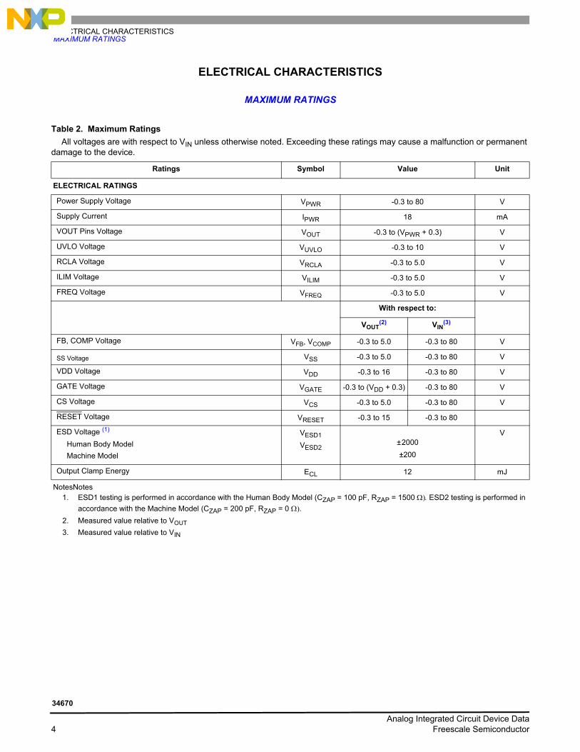
ELECTRICAL CHARACTERISTICSMAXIMUM RATINGS
ELECTRICAL CHARACTERISTICS
MAXIMUM RATINGS
Table 2. Maximum Ratings All voltages are with respect to VIN unless otherwise noted. Exceeding these ratings may cause a malfunction or permanent
damage to the device.
Ratings Symbol Value Unit
ELECTRICAL RATINGS
Power Supply Voltage VPWR -0.3 to 80 V
Supply Current IPWR 18 mA
VOUT Pins Voltage VOUT -0.3 to (VPWR + 0.3) V
UVLO Voltage VUVLO -0.3 to 10 V
RCLA Voltage VRCLA -0.3 to 5.0 V
ILIM Voltage VILIM -0.3 to 5.0 V
FREQ Voltage VFREQ -0.3 to 5.0 V
With respect to:
VOUT(2) VIN
(3)
FB, COMP Voltage VFB, VCOMP -0.3 to 5.0 -0.3 to 80 V
SS Voltage VSS -0.3 to 5.0 -0.3 to 80 V
VDD Voltage VDD -0.3 to 16 -0.3 to 80 V
GATE Voltage VGATE -0.3 to (VDD + 0.3) -0.3 to 80 V
CS Voltage VCS -0.3 to 5.0 -0.3 to 80 V
RESET Voltage VRESET -0.3 to 15 -0.3 to 80
ESD Voltage (1)
Human Body ModelMachine Model
VESD1VESD2
± 2000±200
V
Output Clamp Energy ECL 12 mJ
NotesNotes1. ESD1 testing is performed in accordance with the Human Body Model (CZAP = 100 pF, RZAP = 1500 Ω). ESD2 testing is performed in
accordance with the Machine Model (CZAP = 200 pF, RZAP = 0 Ω).2. Measured value relative to VOUT3. Measured value relative to VIN
Analog Integrated Circuit Device Data 4 Freescale Semiconductor
34670

ELECTRICAL CHARACTERISTICSMAXIMUM RATINGS
THERMAL RATINGS
Operating Temperature
Ambient (4)
Junction (8), (9)
TATJ
-40 to 85120
°C
Storage Temperature TSTG -65 to 150 °C
Power Dissipation (TA = 25 °C) (7) PD 800 mW
Thermal ResistanceJunction to Ambient 20LD SOIC W/B Package (9)
RθJARθJB
10347
°C/W
Peak Package Reflow Temperature During Reflow (5), (6) TPPRT Note 6 °C
Thermal Shutdown Temperature TSHUT 180 °C
Thermal Shutdown Recovery Temperature THYST 150 °C
NotesNotes4. The limiting factor is junction temperature; taking into account the power dissipation, thermal resistance, and heat sinking.5. Pin soldering temperature limit is for 10 seconds maximum duration. Not designed for immersion soldering. Exceeding these limits may
cause malfunction or permanent damage to the device.6. Freescale’s Package Reflow capability meets Pb-free requirements for JEDEC standard J-STD-020C. For Peak Package Reflow
Temperature and Moisture Sensitivity Levels (MSL),Go to www.freescale.com, search by part number [e.g. remove prefixes/suffixes and enter the core ID to view all orderable parts. (i.e. MC33xxxD enter 33xxx), and review parametrics.
7. Maximum power dissipation at indicated ambient temperature in free air with no heatsink used.8. For TA = 85°C and PD = 700 mW and RθJB = 47°C/W.9. Measured with 4 layers 2s2p JEDEC std. PCB.
Table 2. Maximum Ratings (continued)All voltages are with respect to VIN unless otherwise noted. Exceeding these ratings may cause a malfunction or permanent
damage to the device.
Ratings Symbol Value Unit
Analog Integrated Circuit Device Data Freescale Semiconductor 5
34670
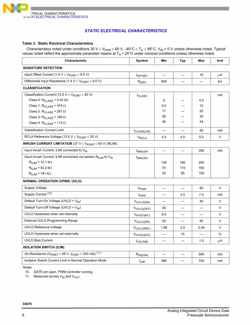
ELECTRICAL CHARACTERISTICSSTATIC ELECTRICAL CHARACTERISTICS
STATIC ELECTRICAL CHARACTERISTICS
Table 3. Static Electrical Characteristics Characteristics noted under conditions 30 V ≤ VPWR ≤ 60 V, - 40°C ≤ TA ≤ 85°C, VIN = 0 V unless otherwise noted. Typical
values noted reflect the approximate parameter means at TA = 25°C under nominal conditions unless otherwise noted.
Characteristic Symbol Min Typ Max Unit
SIGNATURE DETECTION
Input Offset Current (1.4 V ≤ VPORT ≤ 9.5 V) IOFFSET — — 10 µA
Differential Input Resistance (1.4 V ≤ VPORT ≤ 9.5 V) RDIFF 600 — — kΩ
CLASSIFICATION
Classification Current (13.5 V ≤ VPORT ≤ 20 V)Class 0: RCLASS = 4.42 kΩ
Class 1: RCLASS = 475 Ω
Class 2: RCLASS = 261 Ω
Class 3: RCLASS = 169 Ω
Class 4: RCLASS = 113 Ω
ICLASS0
9.0172636
—————
4.012203044
mA
Classification Current Limit ICLASS(LIM) — — 50 mA
RCLA Reference Voltage (13.5 V ≤ VPORT ≤ 20 V) VRCLA 4.0 4.5 5.0 V
INRUSH CURRENT LIMITATION (37 V ≤ VPORT ≤ 60 V) (RLIM)
Input Inrush Current, ILIM connected to VIN IINRUSH — — 350 mA
Input Inrush Current, ILIM connected via resistor RILIM to VIN
RILIM = 12.1 kΩ
RILIM = 42.2 kΩ
RILIM = 191 kΩ
IINRUSH1307030
18011065
250165100
NORMAL OPERATION (VPWR, UVLO)
Supply Voltage VPWR — — 60 V
Supply Current (10) IPWR — 4.5 7.3 mA
Default Turn-On Voltage (UVLO = VIN) VUVLO(ON) — — 40 V
Default Turn-Off Voltage (UVLO = VIN) VUVLO(OFF) 30 — — V
UVLO Hysteresis when set internally VHYST(INT) 6.0 — — V
External UVLO Programming Range VUVLO(PR) 25 — 50 V
UVLO Reference Voltage VUVLO(REF) 1.96 2.0 2.04 V
UVLO Hysteresis when set externally VHYST(EXT) — 15 — %
UVLO Bias Current IUVLO(B) — — 1.0 µA
ISOLATION SWITCH (ILIM)
On-Resistance (VPORT = 48 V, IPORT = 350 mA) (11) RDS(ON) — — 500 mΩ
Isolation Switch Current Limit in Normal Operation Mode ILIM 380 — 700 mA
Notes10. GATE pin open, PWM controller running.11. Measured across VIN and VOUT.
Analog Integrated Circuit Device Data 6 Freescale Semiconductor
34670
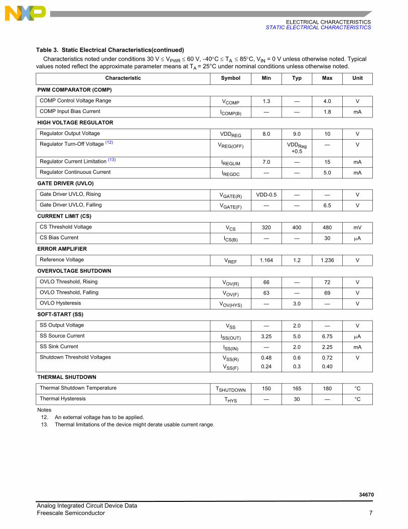
ELECTRICAL CHARACTERISTICSSTATIC ELECTRICAL CHARACTERISTICS
PWM COMPARATOR (COMP)
COMP Control Voltage Range VCOMP 1.3 — 4.0 V
COMP Input Bias Current ICOMP(B) — — 1.8 mA
HIGH VOLTAGE REGULATOR
Regulator Output Voltage VDDREG 8.0 9.0 10 V
Regulator Turn-Off Voltage (12) VREG(OFF) VDDReg+0.5
— V
Regulator Current Limitation (13) IREGLIM 7.0 — 15 mA
Regulator Continuous Current IREGDC — — 5.0 mA
GATE DRIVER (UVLO)
Gate Driver UVLO, Rising VGATE(R) VDD-0.5 — — V
Gate Driver UVLO, Falling VGATE(F) — — 6.5 V
CURRENT LIMIT (CS)
CS Threshold Voltage VCS 320 400 480 mV
CS Bias Current ICS(B) — — 30 µA
ERROR AMPLIFIER
Reference Voltage VREF 1.164 1.2 1.236 V
OVERVOLTAGE SHUTDOWN
OVLO Threshold, Rising VOV(R) 66 — 72 V
OVLO Threshold, Falling VOV(F) 63 — 69 V
OVLO Hysteresis VOV(HYS) — 3.0 — V
SOFT-START (SS)
SS Output Voltage VSS — 2.0 — V
SS Source Current ISS(OUT) 3.25 5.0 6.75 µA
SS Sink Current ISS(IN) — 2.0 2.25 mA
Shutdown Threshold Voltages VSS(R)VSS(F)
0.480.24
0.60.3
0.720.40
V
THERMAL SHUTDOWN
Thermal Shutdown Temperature TSHUTDOWN 150 165 180 °C
Thermal Hysteresis THYS — 30 — °C
Notes12. An external voltage has to be applied.13. Thermal limitations of the device might derate usable current range.
Table 3. Static Electrical Characteristics(continued)Characteristics noted under conditions 30 V ≤ VPWR ≤ 60 V, - 40°C ≤ TA ≤ 85°C, VIN = 0 V unless otherwise noted. Typical
values noted reflect the approximate parameter means at TA = 25°C under nominal conditions unless otherwise noted.
Characteristic Symbol Min Typ Max Unit
Analog Integrated Circuit Device Data Freescale Semiconductor 7
34670
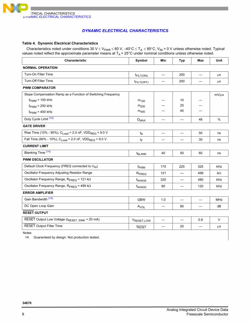
ELECTRICAL CHARACTERISTICSDYNAMIC ELECTRICAL CHARACTERISTICS
DYNAMIC ELECTRICAL CHARACTERISTICS
Table 4. Dynamic Electrical Characteristics Characteristics noted under conditions 30 V ≤ VPWR ≤ 60 V, - 40°C ≤ TA ≤ 85°C, VIN = 0 V unless otherwise noted. Typical
values noted reflect the approximate parameter means at TA = 25°C under nominal conditions unless otherwise noted.
Characteristic Symbol Min Typ Max Unit
NORMAL OPERATION
Turn-On Filter Time tFILT(ON) — 200 — µs
Turn-Off Filter Time tFILT(OFF) — 200 — µs
PWM COMPARATOR
Slope Compensation Ramp as a Function of Switching Frequency
fPWM = 100 kHz
fPWM = 250 kHz
fPWM = 400 kHz
m100m250m400
———
102540
———
mV/µs
Duty Cycle Limit (14) DMAX — — 48 %
GATE DRIVER
Rise Time (10% - 90%), CLoad = 2.0 nF, VDDREG = 9.0 V tR — — 50 ns
Fall Time (90% - 10%), CLoad = 2.0 nF, VDDREG = 9.0 V tF — — 30 ns
CURRENT LIMIT
Blanking Time (14) tBLANK 40 50 60 ns
PWM OSCILLATOR
Default Clock Frequency (FREQ connected to VIN) fPWM 175 225 325 kHz
Oscillator Frequency Adjusting Resistor Range RFREQ 121 — 499 kΩ
Oscillator Frequency Range, RFREQ = 121 kΩ fRANGE 320 — 480 kHz
Oscillator Frequency Range, RFREQ = 499 kΩ fRANGE 80 — 120 kHz
ERROR AMPLIFIER
Gain Bandwidth (14) GBW 1.0 — — MHz
DC Open Loop Gain AVOL — 80 — dB
RESET OUTPUT
RESET Output Low Voltage (IRESET, SINK = 20 mA) VRESET,LOW — — 0.8 V
RESET Output Filter Time tRESET — 20 — µs
Notes14. Guaranteed by design. Not production tested.
Analog Integrated Circuit Device Data 8 Freescale Semiconductor
34670
ELECTRICAL CHARACTERISTICSTYPICAL SWITCHING WAVEFORMS
TYPICAL SWITCHING WAVEFORMS
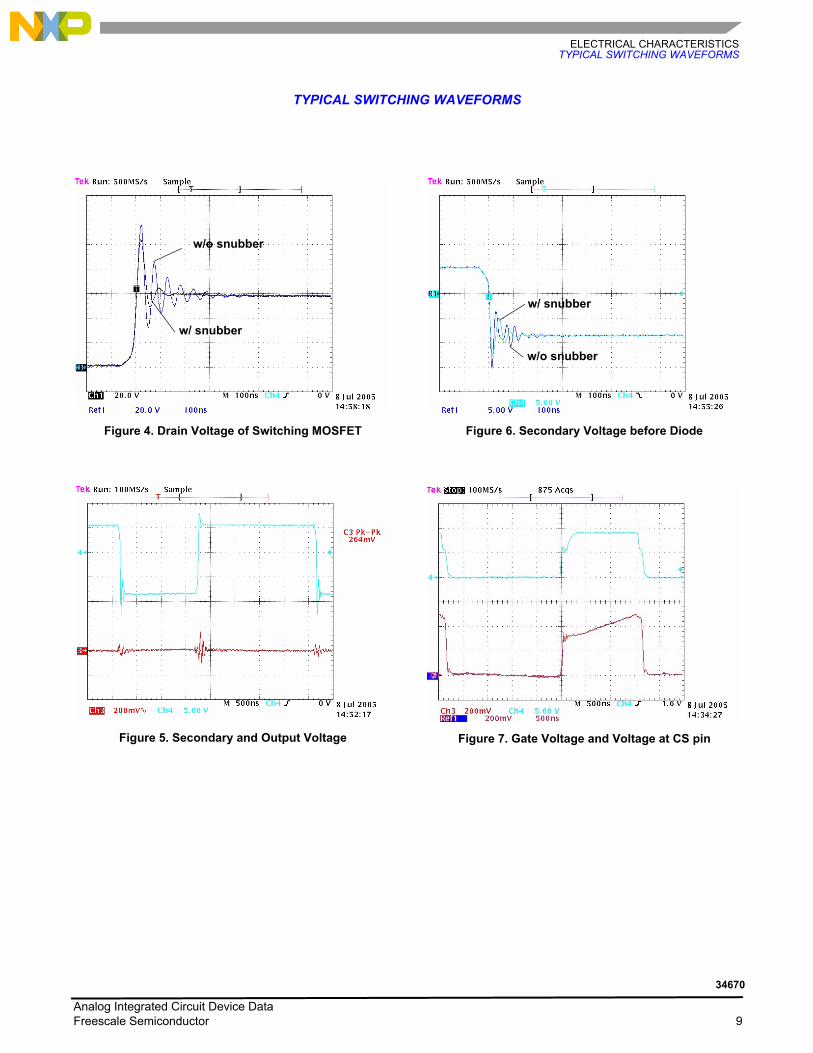
Figure 4. Drain Voltage of Switching MOSFET
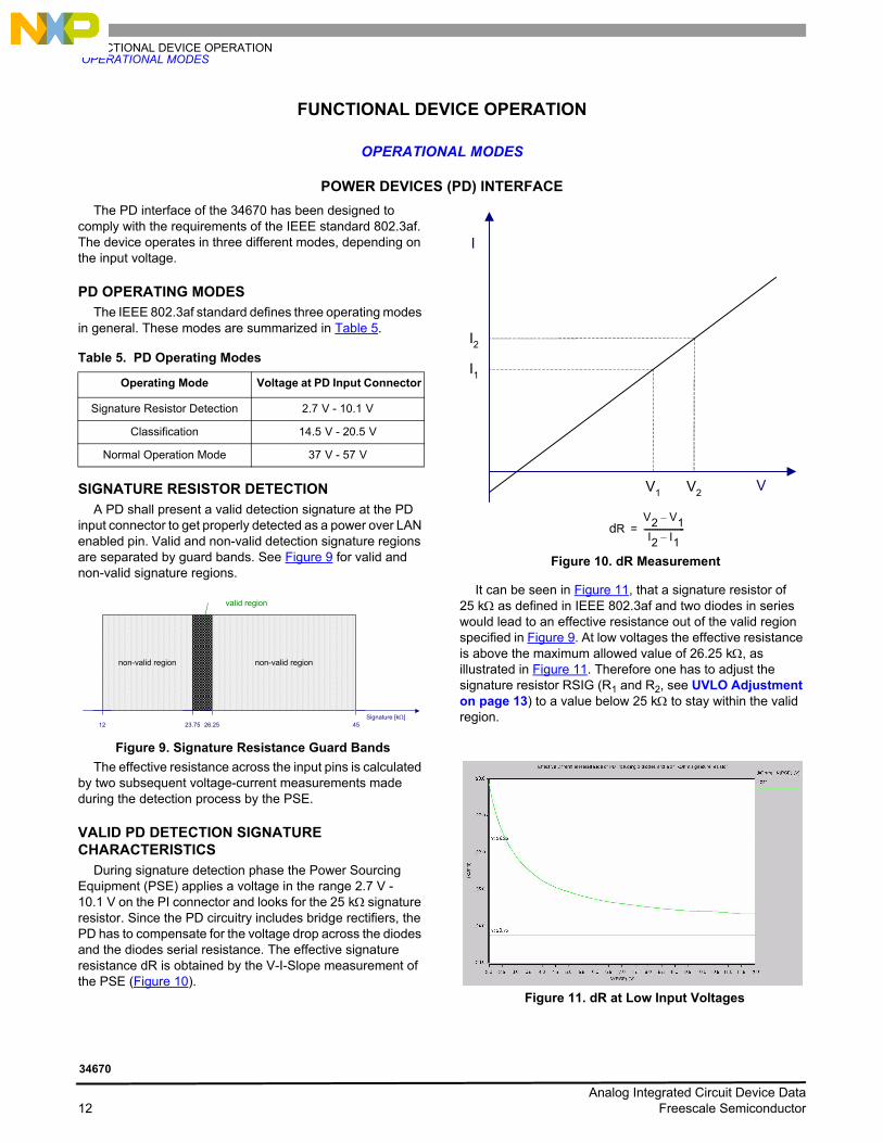
Figure 5. Secondary and Output Voltage
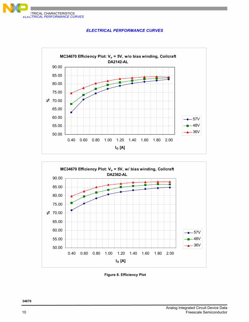
Figure 6. Secondary Voltage before Diode
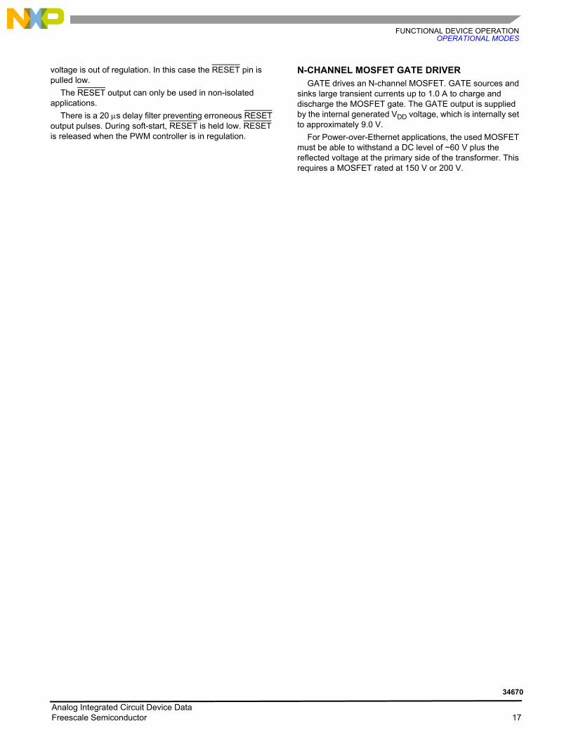
Figure 7. Gate Voltage and Voltage at CS pin
w/o snubber
w/ snubber
w/ snubber
w/o snubber
Analog Integrated Circuit Device Data Freescale Semiconductor 9
34670
ELECTRICAL CHARACTERISTICSELECTRICAL PERFORMANCE CURVES
ELECTRICAL PERFORMANCE CURVES
Figure 8. Efficiency Plot
MC34670 Efficiency Plot: Vo = 5V, w/ bias winding, Coilcraft DA2362-AL
50.00
55.00
60.00
65.00
70.00
75.00
80.00
85.00
90.00
0.40 0.60 0.80 1.00 1.20 1.40 1.60 1.80 2.00
IO [A]
%
57V48V36V
MC34670 Efficiency Plot: Vo = 5V, w/o bias winding, Coilcraft DA2142-AL
50.00
55.00
60.00
65.00
70.00
75.00
80.00
85.00
90.00
0.40 0.60 0.80 1.00 1.20 1.40 1.60 1.80 2.00
IO [A]
%
57V48V36V
Analog Integrated Circuit Device Data 10 Freescale Semiconductor
34670

FUNCTIONAL DESCRIPTIONINTRODUCTION
FUNCTIONAL DESCRIPTION
INTRODUCTION
The 34670 combines a Power Interface Port for IEEE 802.3af Powered Devices (PD) and a high performance current mode switching regulator. It allows a designer to build PDs with a minimum of external components by means of integrating the required IEEE 802.3af functions and all functions necessary to build a high efficiency DC/DC converter. Thus 34670 gives the system designer a device that drastically reduces cost and board space.
On the PD side the 34670 fully supports the IEEE802.3af standard and provides complete signature detection and power classification functions. It controls inrush current limiting and incorporates an adjustable undervoltage lockout. The 34670 includes thermal protection circuitry to protect the device in case of high power dissipation.
The 34670 also offers an input overvoltage detection to protect the external switching MOSFET by disabling the gate driver in case of input line overvoltage.
The switching regulator provides excellent line and load regulation. It drives an external power MOSFET with sense resistor. The switching frequency is adjustable between 100 kHz and 400 kHz. The output voltage feedback information can be accomplished by an optocoupler, if isolation is required.
An internal logic control block manages the sequencing of signature detection, classification and proper turn on and turn off of the DC/DC converter.
FUNCTIONAL PIN DESCRIPTION
POSITIVE SUPPLY VOLTAGE INPUT (VPWR)This is the most positive power supply input. The load
connects between this pin and the VOUT pin.
CLASSIFICATION RESISTOR (RCLA)Connect a resistor between RCLA and VIN to select the
class of the PD.
UNDERVOLTAGE LOOKOUT (UVLO)Used to adjust the undervoltage lookout threshold voltage,
connected to VIN to use the default threshold voltage.
TEST PINS (TEST1, TEST2)Connect to VIN in application mode.
FREQUENCY ADJUSTMENT (FREQ)Adjusts the internal oscillator frequency by connecting a
resistor between FREQ and VIN.
INRUSH CURRENT LIMIT (ILIM)Used to adjust the inrush current limit of the isolation
switch, add a resistor between ILIM and VIN.
NEGATIVE SUPPLY VOLTAGE (VIN)This is the most negative power supply input.
OUTPUT VOLTAGE (VOUT)This pin is the drain of the internal Power MOSFET (high
current path and low current path).
RESET OUTPUT (RESET)This is an active-low RESET output signal. This pin is
referenced to VOUT.
SOFT START INPUT (SS)Connect an external capacitor to SS. The internal current
source charges the capacitor and generates a soft-start ramp.
COMPENSATION PIN (COMP)COMP is the output of the error amplifier and is available
for feedback compensation. COMP is pulled-up by an internal 5.0 kΩ resistor to 5.0 V.
FEEDBACK INPUT (FB)This is the inverting input of the error amplifier. In non-
isolated applications it’s connected to the secondary output through a resistor divider.
CURRENT SENSE (CS)The current sense pin CS senses a voltage that is
proportional to the current through the sense resistor.
GATE DRIVER OUTPUT (GATE)GATE drives the gate of the external power MOSFET.
GATE sources and sinks up to 1.0 A.
VDD OUTPUT (VDD)VDD mainly supplies the gate of the external power
MOSFET. Connect a capacitor from VDD to VOUT.
Analog Integrated Circuit Device Data Freescale Semiconductor 11
34670
FUNCTIONAL DEVICE OPERATIONOPERATIONAL MODES
FUNCTIONAL DEVICE OPERATION
OPERATIONAL MODES
POWER DEVICES (PD) INTERFACEThe PD interface of the 34670 has been designed to
comply with the requirements of the IEEE standard 802.3af. The device operates in three different modes, depending on the input voltage.
PD OPERATING MODESThe IEEE 802.3af standard defines three operating modes
in general. These modes are summarized in Table 5.
SIGNATURE RESISTOR DETECTIONA PD shall present a valid detection signature at the PD
input connector to get properly detected as a power over LAN enabled pin. Valid and non-valid detection signature regions are separated by guard bands. See Figure 9 for valid and non-valid signature regions.
Figure 9. Signature Resistance Guard BandsThe effective resistance across the input pins is calculated
by two subsequent voltage-current measurements made during the detection process by the PSE.
VALID PD DETECTION SIGNATURE CHARACTERISTICS
During signature detection phase the Power Sourcing Equipment (PSE) applies a voltage in the range 2.7 V - 10.1 V on the PI connector and looks for the 25 kΩ signature resistor. Since the PD circuitry includes bridge rectifiers, the PD has to compensate for the voltage drop across the diodes and the diodes serial resistance. The effective signature resistance dR is obtained by the V-I-Slope measurement of the PSE (Figure 10).
It can be seen in Figure 11, that a signature resistor of 25 kΩ as defined in IEEE 802.3af and two diodes in series would lead to an effective resistance out of the valid region specified in Figure 9. At low voltages the effective resistance is above the maximum allowed value of 26.25 kΩ, as illustrated in Figure 11. Therefore one has to adjust the signature resistor RSIG (R1 and R2, see UVLO Adjustment on page 13) to a value below 25 kΩ to stay within the valid region.
Figure 11. dR at Low Input Voltages
Table 5. PD Operating Modes
Operating Mode Voltage at PD Input Connector
Signature Resistor Detection 2.7 V - 10.1 V
Classification 14.5 V - 20.5 V
Normal Operation Mode 37 V - 57 V
Signature [kΩ]
non-valid region
12 23.75 26.25 45
non-valid region
valid region
I
V
I1
I2
V1 V2
RdV2 V1–
I2 I1–---------------------=
Figure 10. dR Measurement
Analog Integrated Circuit Device Data 12 Freescale Semiconductor
34670

FUNCTIONAL DEVICE OPERATIONOPERATIONAL MODES
CLASSIFICATIONA PD may optionally be classified by the PSE. The intent
of classification is to provide a method for more efficient power allocation through the PSE. The PD classification allows the PSE to identify four different (power) classes depending on the required power that the PD will draw during normal operation. The classes and the corresponding maximum power drawn by the PD is shown in Table 6.
Table 6. PD Classes
PD CLASSESDuring classification probing by the PSE, the PD applies
the appropriate load current onto the line. The PSE measures the load current and can determine the classification as described in Table 7.
.
CLASSIFICATION SIGNATURE LOAD CURRENTThe implementation for the classification circuitry is shown
in Figure 12.
Figure 12. Classification CircuitryA constant voltage is applied at pin RCLA and depending
on the resistor RCLASS, a current from +VPORT to -VPORT is flowing with the following relation:
ICLASS is the classification current that is measured by the PSE. The values for the RCLASS resistor corresponding to the appropriate class are listed in Table 8.
UVLO ADJUSTMENTThe 34670 has default UVLO settings that corresponds to
the IEEE 802.3af standard. Nevertheless the user can adjust the UVLO by an external resistor divider as sketched in Figure 13. Since the UVLO resistor divider replaces the
Class Usage Maximum Power [W]
0 Default 0.44 - 12.95
1 Optional 0.44 - 3.84
2 Optional 3.84 - 6.49
3 Optional 6.49 - 12.95
4 Reserved —
Table 7. PD Class vs. Classification Current
ClassClassification Current [mA]
ConditionMin Max
0 0 4 14.5 - 20.5 Volts measured at PD input connector1 9 12
2 17 20
3 26 30
4 36 44
Table 8. PD Class vs. Classification Resistor RCLASS
Class Classification Current [mA] RCLASS [Ω]
0 2.0 4.42k
1 10.5 475
2 18.5 261
3 28 169
4 40 113
+VPORT
-VPORT
RCLASS
RCLA
VPWR
VIN
34670
Vref
-
+
ICLASS
EN
ICLASSVRCLA
RCLASS---------------------=
Analog Integrated Circuit Device Data Freescale Semiconductor 13
34670

FUNCTIONAL DEVICE OPERATIONOPERATIONAL MODES
signature resistor, the total resistance of R1+R2 must equal 25 kΩ.
Figure 13. UVLO Adjustment by ExternalResistor Divider
To use the default settings for UVLO, the pin UVLO must be connected to VIN. In this case, a valid signature resistor has to be placed between -VPORT and +VPORT. This configuration can be seen in Figure 14.
Figure 14. Default UVLO Settings
To calculate the values for R1 and R2 the following equations should be used:
where VUVLO(ON) is the desired turn-on voltage threshold and VUVLO(ref) the UVLO reference voltage.
The typical turn-off voltage VUVLO(OFF) is 85% of the turn on voltage VUVLO(ON).
INRUSH CURRENT LIMITATION
The 34670 has been designed to interface also with legacy PoE-PSEs which do not meet the inrush current requirement of the IEEE 802.3af specification. By setting the initial inrush current limit to a low level, a PD using the 34670 minimizes the current drawn from the PSE during start-up. The maximum inrush current level can be set by connecting a resistor from ILIM to VIN as illustrated in Figure 15.
Figure 15. Inrush Current Limitation by External Resistor RILIM
The following table shows the selectable current limits and the corresponding resistor value that has to be connected between pins ILIM and VIN:
After powering up, the 34670 switches to the high level current limit, thereby allowing the PD to consume up to 12.95 W if a 802.3af PSE is present.
PULSE WITH MODULATOR CONTROLLER
CURRENT-MODE CONTROL OPERATIONThe 34670 offers current-mode control operation with
leading-edge blanking. The current-limit comparator monitors the CS pin at all times and provides cycle-by-cycle current limit.
The CS signal contains a leading-edge spike that is the result of the MOSFET gate charge current, capacitive and
diode reverse recovery current of the power circuit. The leading-edge blanking of the CS signal prevents the PWM comparator from premature termination of the on cycle.
The 34670 limits the duty cycle to 50%. This is advantageous for applications which are not allowed to exceed an on-time of 50 % of the switching period TS. Beside the duty-cycle limit, slope compensation is provided to stabilize the inner current loop and avoid oscillations for
R2
R1
-VPORT
+VPORT
RCLA
VPWR
UVLO
ILIM
VIN
RSIG25kΩ
-VPORT
+VPORT
RCLA
VPWR
UVLO
ILIM
VIN
R1 R2+ RSIG=
R2VUVLO REF( )VUVLO ON( )---------------------------------- RSIG⋅=
Table 9. Inrush Current Limit vs. RILIM
Inrush Current Limit [mA] RILIM Value [kΩ]
180 12.1
110 42.2
65 191
R1 RSIG R2–=
VUVLO OFF( ) VUVLO ON( ) 0.85⋅=
RSIG25kΩ
-VPORT
+VPORT
RCLA
VPWR
UVLO
ILIM
VIN
RILIM
RCLASS
Analog Integrated Circuit Device Data 14 Freescale Semiconductor
34670

FUNCTIONAL DEVICE OPERATIONOPERATIONAL MODES
converters running in continuos conduction mode (CCM). The value of the slope compensation depends on the switching frequency. See Table 10.
ISOLATED OPTOCOUPLER FEEDBACK
Isolated voltage feedback can be accomplished by using an optocoupler and a shunt regulator (see Figure 19). The output voltage accuracy is a function of the accuracy of the shunt regulator and feedback resistor divider tolerance, therefore the feedback resistors should have an appropriate accuracy.
Since the error amplifier function is implemented on the secondary side by the optocoupler and a 3-pin adjustable shunt regulator, the internal error amplifier of the 34670 is not used. The FB pin is connected to VOUT, thus disabling the internal open-drain error amplifier.
The bias voltage for the optocoupler is accomplished through the internal 5.0 kΩ pull-up resistor between COMP and an internal 5.0 V reference.
When a TL431 or TLV431 shunt regulator is used for output voltage regulation, the output voltage is set by the ratio of resistors R1 and R2, see Figure 16 for details. The output voltage is given by the following equation:
where VREF = 1.24 V for the TLV431 (VREF = 2.5 V for the TL431).
Figure 16. Isolated Optocoupler Feedback
ISOLATED PRIMARY CONTROL FEEDBACKAnother option to accomplish isolated feedback is the use
of a tertiary winding (see Figure 21). The advantage of this solution without optocoupler and shunt regulator is clearly the cost effectiveness. Nevertheless the line and load regulation is worse than with optocoupler feedback.
When isolated primary feedback is used, the loop compensation components are connected between pins COMP and FB.
INTERNAL REGULATORSThe internal high voltage regulator of the 34670 regulates
from the input voltage across VPWR and VIN down to the VDD voltage. During start-up the high voltage regulator provides the necessary voltage for the internal gate driver to commence switching. If the external MOSFET gate drive pulls less than 3.0 mA under all circumstances, an auxiliary transformer winding that usually provides the bias voltage for the chip and the gate driver is not required.
In cases where the external MOSFET gate drive pulls more than 5.0 mA, an auxiliary winding is needed to reduce the power dissipation in the internal high voltage LDO. See Figure 18 for an application drawing. It is recommended to add a 0.1 µF ceramic capacitor in parallel with the existing load capacitor. This reduces noise at the VDD pin caused by the auxiliary winding.
The high voltage regulator is disabled when the VDD pin is forced by an external voltage above the VDD regulation point.
Table 10. Slope Compensation Values
Switching Frequency [kHz] Slope Compensation [mV/µs]
100 10
250 25
400 50
VO VREF 1R1R2-------+
⎝ ⎠⎜ ⎟⎛ ⎞
⋅=
T1
NP NS
RV
R1
TLV431R2
Analog Integrated Circuit Device Data Freescale Semiconductor 15
34670

FUNCTIONAL DEVICE OPERATIONOPERATIONAL MODES
This reduces power dissipation in the device and improves overall efficiency.
Figure 17. VDD and MOSFET Driver Output Behavior
A load capacitor connected to VDD ensures a proper filtering of the VDD voltage. The minimum capacitance value for this load capacitor should be at least 10 µF. An electrolytic type capacitor is sufficient.
Please refer to application note A/N3279 for further information about the size of the capacitor.
If VDD falls below the UVLO threshold, the voltage regulator is disabled and the MOSFET driver output (GATE) is held low.
PWM CONTROLLER UVLO, SOFT-START, AND SHUTDOWN FUNCTION
The soft-start function provided by the 34670 allows the output voltage to ramp up in a controlled way, thus eliminating output voltage overshoot.
While the PWM controller is in undervoltage lockout, the capacitor CSS connected to the SS pin is fully discharged. After coming out of undervoltage lockout, an internal current source starts charging the capacitor CSS to initiate soft-start. When VSS has reached 0.6 V, the gate driver is enabled and PWM operation begins. The duty cycle during soft-start is primarily controlled by the internal sawtooth voltage and the voltage at the SS pin. If the voltage at the SS pin is above 2.6 V, the regular PWM control through pins CS, COMP, and FB takes over and soft-start is finished.
The following equation calculates the total soft-start time:
OVERVOLTAGE SHUTDOWN
The 34670 includes an overvoltage protection (OVP) feature that turns off the external MOSFET when the input voltage exceeds the overvoltage threshold.
When the overvoltage protection is triggered (VPWR > VOV(R)), the gate driver is immediately disabled. At the same time, the slow discharge of CSS is initiated. While the soft-start capacitor is discharging, the gate driver remains disabled. Once VSS = 0.3 V and the overvoltage (VPWR < VOV(F)) condition disappears, operation resumes through a regular soft-start.
CURRENT-SENSE COMPARATORThe current-sense (CS) comparators and its associated
circuitry limits the peak current through the MOSFET. Current is sensed at CS pin as a voltage across the sense resistor RCS between the source of the MOSFET and VOUT.
The CS input has two voltage trip levels, a 600mV high limit and a 400 mV low limit. When the voltage on CS produced by a current through the current sense resistor exceeds the high limit threshold, the current ON-cycle is immediately terminated and the GATE output is pulled low.
If the low limit threshold is exceeded for longer than 50 ns (typical blanking time), the current ON-cycle is also terminated. The blanking time ensures a false termination of the switching cycle caused by the leading-edge spike on the sense waveform.
The current-sense resistor RCS is selected according to the following equation:
where ILIM(primary) is the maximum peak primary-side current.
In case of an overcurrent in the external MOSFET the current switching cycle is terminated and GATE is pulled low. The soft-start capacitor CSS is discharged and after removal of the faulty condition the PWM is re-started through a regular soft start.
PWM OSCILLATOR
A default 250 kHz oscillator sets the switching frequency of the PWM controller. The frequency of the oscillator can be adjusted between 100 kHz and 400 kHz by an optional external resistor RFREQ connected from the FREQ pin of the integrated circuit to VIN.
The appropriate switching frequency fPWM can be calculated as shown below:
where fPWM is the PWM switching frequency and RFREQ is the frequency adjusting resistor.
To use the default frequency of 250 kHz the FREQ pin can be connected to VIN or can be left open.
RESET OUTPUT
The RESET pin is an open drain output. The reset control circuit supervises the FB voltage and recognizes if the output
HVReg enable
GATE enable
10
2
4
6
8
VGATE(R)
VREG(OFF)
12
VGATE(F)
V DD
t
tSS ms[ ] 0.4 CSS nF[ ]⋅=
RCS400mV
ILIM primary( )----------------------------------------=
fPWM kHz[ ] 47920RFREQ kΩ[ ]------------------------------------ 4+=
Analog Integrated Circuit Device Data 16 Freescale Semiconductor
34670
FUNCTIONAL DEVICE OPERATIONOPERATIONAL MODES
voltage is out of regulation. In this case the RESET pin is pulled low.
The RESET output can only be used in non-isolated applications.
There is a 20 µs delay filter preventing erroneous RESET output pulses. During soft-start, RESET is held low. RESET is released when the PWM controller is in regulation.
N-CHANNEL MOSFET GATE DRIVERGATE drives an N-channel MOSFET. GATE sources and
sinks large transient currents up to 1.0 A to charge and discharge the MOSFET gate. The GATE output is supplied by the internal generated VDD voltage, which is internally set to approximately 9.0 V.
For Power-over-Ethernet applications, the used MOSFET must be able to withstand a DC level of ~60 V plus the reflected voltage at the primary side of the transformer. This requires a MOSFET rated at 150 V or 200 V.
Analog Integrated Circuit Device Data Freescale Semiconductor 17
34670
TYPICAL APPLICATIONS
TYPICAL APPLICATIONS
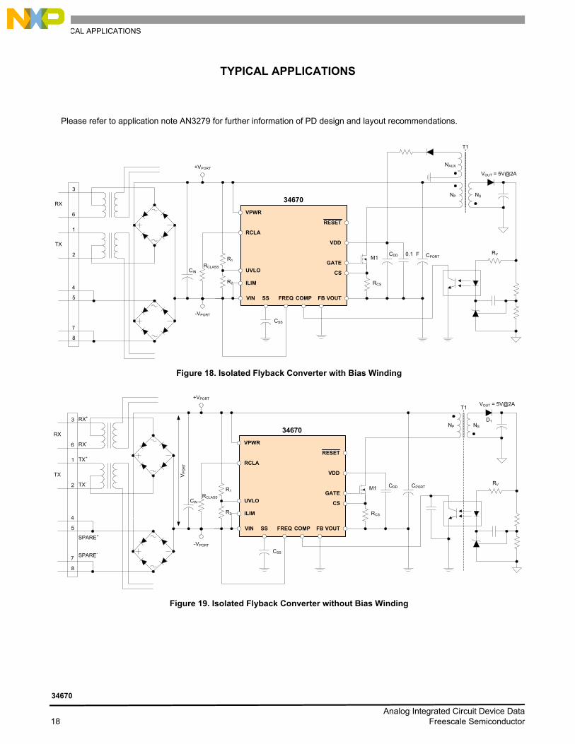
Please refer to application note AN3279 for further information of PD design and layout recommendations.
Figure 18. Isolated Flyback Converter with Bias Winding
Figure 19. Isolated Flyback Converter without Bias Winding
3
6
1
2
4
5
8
7
RX
TX
CPORT
RCLASS
M1
RCS
T1
VOUT = 5V@2A
R2
R1
NP NS
NAUX
-VPORT
+VPORT
CSS
CIN
RVCDD 0.1 F
SS
VPWR
RCLA
UVLO
ILIM
VIN VOUTFB
CS
GATE
VDD
FREQ
RESET
COMP
34670
3
6
1
2
4
5
8
7
RX
TX
CPORT
RCLASS
M1
RCS
T1 VOUT = 5V@2A
R2
R1CDD
D1NP NS
RV
-VPORT
+VPORT
CSS
CIN
RX+
RX-
TX+
TX-
SPARE+
SPARE-
VP
OR
T
SS
VPWR
RCLA
UVLO
ILIM
VIN VOUTFB
CS
GATE
VDD
FREQ
RESET
COMP
34670
Analog Integrated Circuit Device Data 18 Freescale Semiconductor
34670
TYPICAL APPLICATIONS
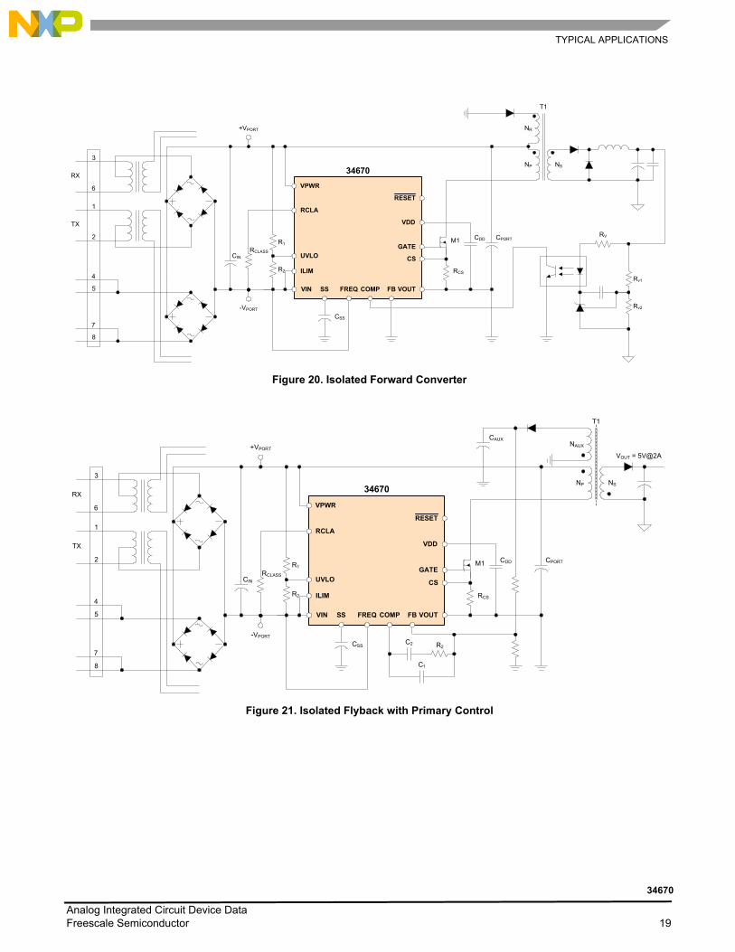
Figure 20. Isolated Forward Converter
Figure 21. Isolated Flyback with Primary Control
3
6
1
2
4
5
8
7
RX
TX
CPORT
RCLASS
M1
RCS
T1
R2
R1CDD
NP NS
RV
Rv1
-VPORT
+VPORT
Rv2
CSS
CIN
NR
SS
VPWR
RCLA
UVLO
ILIM
VIN VOUTFB
CS
GATE
VDD
FREQ
RESET
COMP
34670
3
6
1
2
4
5
8
7
RX
TX
CPORT
RCLASS
M1
RCS
T1
VOUT = 5V@2A
R2
R1CDD
NP NS
NAUX
-VPORT
+VPORT
CSS
CIN
C2
C1
R2
CAUX
SS
VPWR
RCLA
UVLO
ILIM
VIN VOUTFB
CS
GATE
VDD
FREQ
RESET
COMP
34670
Analog Integrated Circuit Device Data Freescale Semiconductor 19
34670

TYPICAL APPLICATIONS
Figure 22. Non-Isolated Flyback Converter
3
6
1
2
4
5
8
7
RX
TX
CPORT
RCLASS
M1
RCS
T1
CO
VOUT = 5V@2A
R4
R3CDD
D1NP NS
R1
-VPORT
+VPORT
RbCSS
CIN
C2
C1
R2
SS
VPWR
RCLA
UVLO
ILIM
VIN VOUTFB
CS
GATE
VDD
FREQ
RESET
COMP
34670
Analog Integrated Circuit Device Data 20 Freescale Semiconductor
34670
REFERENCE DOCUMENTS
REFERENCE DOCUMENTS
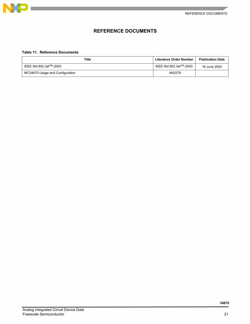
Table 11. Reference Documents
Title LIterature Order Number Publication Date
IEEE Std 802.3af™-2003 IEEE Std 802.3af™-2003 18 June 2003
MC34670 Usage and Configuration AN3279
Analog Integrated Circuit Device Data Freescale Semiconductor 21
34670
PACKAGINGPACKAGE DIMENSIONS
PACKAGING
PACKAGE DIMENSIONS
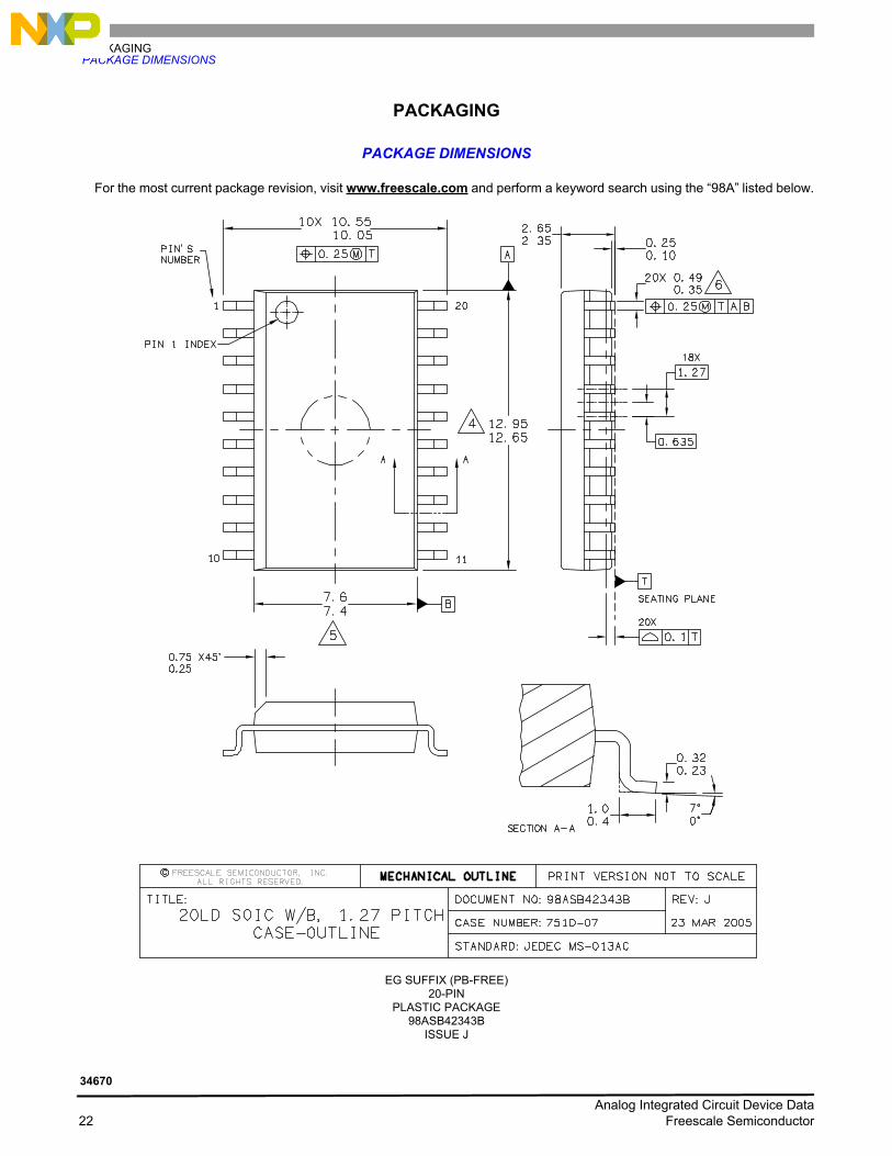
For the most current package revision, visit www.freescale.com and perform a keyword search using the “98A” listed below.
EG SUFFIX (PB-FREE)20-PIN
PLASTIC PACKAGE98ASB42343B
ISSUE J
Analog Integrated Circuit Device Data 22 Freescale Semiconductor
34670

REVISION HISTORY
REVISION HISTORY
Revision Date Description of Changes
1.0 8/2006 • Initial release
2.0 9/2006 • Change to UVLO Hysteresis when set internally on page 6, Regulator Current Limitation (13) on page 7, OVLO Threshold, Rising on page 7, OVLO Threshold, Falling on page 7, Shutdown Threshold Voltages on page 7, and Default Clock Frequency (FREQ connected to VIN) on page 8
• Changed Data Sheet category to “Advanced Information*”
3.0 12/2006 • Typ and Max change to RCLA Reference Voltage (13.5 V ≤ VPORT ≤ 20 V) on page 6• Deleted Oscillator Frequency Adjusting Resistor Range in Static Electrical
Characteristics• Split Oscillator Frequent Range into two parameters, Oscillator Frequency Range,
RFREQ = 121 kΩ on page 8 and Oscillator Frequency Range, RFREQ = 499 kΩ on page 8• Added note to Duty Cycle Limit (14) on page 8, Blanking Time (14) on page 8, and Gain
Bandwidth (14) on page 8• Changed nomenclature for Peak Package Reflow Temperature During Reflow (5), (6) on
page 5• Changed name and value for Thermal Shutdown Recovery Temperature on page 5
Analog Integrated Circuit Device Data Freescale Semiconductor 23
34670

MC34670Rev. 3.012/2006
Information in this document is provided solely to enable system and software implementers to use Freescale Semiconductor products. There are no express or implied copyright licenses granted hereunder to design or fabricate any integrated circuits or integrated circuits based on the information in this document.
Freescale Semiconductor reserves the right to make changes without further notice to any products herein. Freescale Semiconductor makes no warranty, representation or guarantee regarding the suitability of its products for any particular purpose, nor does Freescale Semiconductor assume any liability arising out of the application or use of any product or circuit, and specifically disclaims any and all liability, including without limitation consequential or incidental damages. “Typical” parameters that may be provided in Freescale Semiconductor data sheets and/or specifications can and do vary in different applications and actual performance may vary over time. All operating parameters, including “Typicals”, must be validated for each customer application by customer’s technical experts. Freescale Semiconductor does not convey any license under its patent rights nor the rights of others. Freescale Semiconductor products are not designed, intended, or authorized for use as components in systems intended for surgical implant into the body, or other applications intended to support or sustain life, or for any other application in which the failure of the Freescale Semiconductor product could create a situation where personal injury or death may occur. Should Buyer purchase or use Freescale Semiconductor products for any such unintended or unauthorized application, Buyer shall indemnify and hold Freescale Semiconductor and its officers, employees, subsidiaries, affiliates, and distributors harmless against all claims, costs, damages, and expenses, and reasonable attorney fees arising out of, directly or indirectly, any claim of personal injury or death associated with such unintended or unauthorized use, even if such claim alleges that Freescale Semiconductor was negligent regarding the design or manufacture of the part.
Freescale™ and the Freescale logo are trademarks of Freescale Semiconductor, Inc. All other product or service names are the property of their respective owners.© Freescale Semiconductor, Inc., 2006. All rights reserved.
How to Reach Us:
Home Page:www.freescale.com
Web Support:http://www.freescale.com/support
USA/Europe or Locations Not Listed:Freescale Semiconductor, Inc.Technical Information Center, EL5162100 East Elliot Road Tempe, Arizona 85284 +1-800-521-6274 or +1-480-768-2130www.freescale.com/support
Europe, Middle East, and Africa:Freescale Halbleiter Deutschland GmbHTechnical Information CenterSchatzbogen 781829 Muenchen, Germany+44 1296 380 456 (English)+46 8 52200080 (English)+49 89 92103 559 (German)+33 1 69 35 48 48 (French)www.freescale.com/support
Japan:Freescale Semiconductor Japan Ltd. Headquarters ARCO Tower 15F 1-8-1, Shimo-Meguro, Meguro-ku, Tokyo 153-0064Japan0120 191014 or +81 3 5437 [email protected]
Asia/Pacific:Freescale Semiconductor Hong Kong Ltd.Technical Information Center 2 Dai King Street Tai Po Industrial Estate Tai Po, N.T., Hong Kong +800 2666 [email protected]
For Literature Requests Only:Freescale Semiconductor Literature Distribution CenterP.O. Box 5405Denver, Colorado 802171-800-441-2447 or 303-675-2140Fax: [email protected]