mc33882, six output low-side switch with spi and parallel ... · six output low-side switch with...
TRANSCRIPT

Document Number: MC33882Rev. 11.0, 11/2014
Freescale SemiconductorTechnical Data
Six Output Low-side Switch with SPI and Parallel Input Control
The 33882 is a smart 6 output low-side switch able to control system loads up to 1.0 A. The six outputs can be controlled via both serial peripheral interface (SPI) and parallel input control, making the device attractive for fault tolerant system applications. There are two additional 30 mA low-side switches with SPI diagnostic reporting (parallel input control only).
The 33882 is designed to interface directly with industry standard microcontrollers via SPI to control both inductive and incandescent loads. Outputs are configured as open drain power MOSFETs incorporating internal dynamic clamping and current limiting. The device has multiple monitoring and protection features, including low standby current, fault status reporting, internal 52 V clamp on each output, output specific diagnostics, and protective shutdown. Additionally, it has a mode select pin affording a dual means of input control.
Features
• Outputs clamped for switching inductive loads• Very low operational bias currents (< 2.0 mA)• CMOS input logic compatible with 5.0 V logic levels• Robust load dump (60 V transient at VPWR on OUT0 – OUT5)• Daisy chain operation of multiple devices possible• Switch outputs can be paralleled for higher currents• RDS(ON) of 0.4 per output (25 °C) at 13 V VPWR
• SPI operation guaranteed to 2.0 MHz
Figure 1. 33882 Simplified Application Diagram
SIX OUTPUT LOW-SIDE SWITCH
VW SUFFIX (PB-FREE)
98ASH70693A30-PIN HSOP
33882
ORDERING INFORMATION
Device (For Tape and
Reel, add an R2 Suffix)
Temperature Range (TA)
Package
MC33882PVW
-40 °C to 125 °C
30 HSOP
MC33882PEP 32 QFN
MC33882PEK 32 SOICW-EP
EP SUFFIX (PB-FREE)
98ASA00706D32-PIN QFN
EK SUFFIX(PB-FREE)
98ARL10543D32-PIN SOICW
VPWR
VDD
CS
SCLK
SI
SO
IN0
MODE
IN1
IN2
IN3
IN4
IN5
IN6
IN7
OUT0
IN0 & IN1
IN2 & IN3
IN4 & IN5
GND
33882
VDD VPWR
Optional ParallelControl of
Outputs 0 through 7
High PowerOutputs
Low PowerLED
Outputs
Optional Controlof Paired Outputs
MCU
OUT1OUT2
OUT3
OUT4
OUT5
OUT6
OUT7
© Freescale Semiconductor, Inc., 2006 - 2014. All rights reserved.
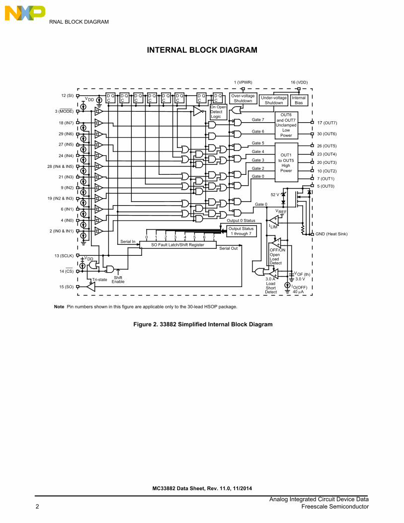
INTERNAL BLOCK DIAGRAM
INTERNAL BLOCK DIAGRAM
Figure 2. 33882 Simplified Internal Block Diagram
-+
-+
+ -
17 (OUT7)
30 (OUT6)
26 (OUT5)
23 (OUT4)
20 (OUT3)
10 (OUT2)
7 (OUT1)
5 (OUT0)
16 (VDD)1 (VPWR)
12 (SI)
3 (MODE)
18 (IN7)
29 (IN6)
24 (IN4)
28 (IN4 & IN5)
21 (IN3)
27 (IN5)
9 (IN2)
19 (IN2 & IN3)
6 (IN1)
4 (IN0)
2 (IN0 & IN1)
13 (SCLK)
14 (CS)
15 (SO)
Serial Out
Serial In
D D D D D D D DC C C C C C C C
Q Q Q Q Q Q Q QDDV
DDV
Tri-state ShiftEnable
SO Fault Latch/Shift Register
Output 0 Status
Output Status1 through 7
Gate 0
Gate 0
Gate 2
Gate 3
Gate 4
Gate 5
Gate 6
Gate 7
Over-voltageShutdown
Under-voltageShutdown
InternalBias
DetectLogic
On Open
OpenLoad
OFF/ON
Detect
LoadShort
3.0 A
Detect
REFV
LIMI
OF (th)V
O(OFF)I40 A
3.0 V
52 V
OUT6and OUT7Unclamped
LowPower
OUT1to OUT5
Power
0 1 2 3 4 5 6 7GND (Heat Sink)
Note Pin numbers shown in this figure are applicable only to the 30-lead HSOP package.
High
MC33882 Data Sheet, Rev. 11.0, 11/2014
Analog Integrated Circuit Device Data2 Freescale Semiconductor

PIN CONNECTIONS
PIN CONNECTIONS
Figure 3. HSOP, QFN, and SOIC Pin Connections
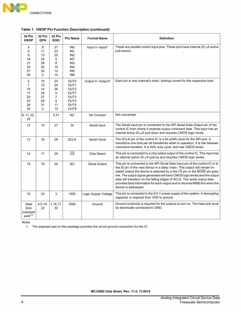
Table 1. HSOP Pin Function Description
30 Pin HSOP
32 Pin QFN
32 Pin SOIC
Pin Name Formal Name Definition
1 6 18 VPWR Load Supply Voltage This pin is connected to battery voltage. A decoupling cap is required from VPWR to ground.
21928
7261
196
13
IN0 & IN1IN2 & IN3IN4 & IN5
Input 0 & Input 1Input 2 & Input 3Input 4 & Input 5
These input pins control two output channels each when the MODE pin is pulled high. These pins may be connected to pulse width modulated (PWM) outputs of the control IC while the MODE pin is high. The states of these pins are ignored during normal operation (MODE pin low), and override the normal inputs (serial or parallel) when the MODE pin is high. These pins have internal active 25 A pull-downs.
3 8 20 MODE Mode Select The MODE pin is connected to the MODE pin of the control IC. This pin has an internal active 25 A pull-up.
123456789101112131415
302928272625242322212019181716
VPWRIN0&IN1
MODEIN0
OUT0IN1
OUT1NCIN2
OUT2NCSI
SCLKCSSO
OUT6IN6IN4&IN5IN5OUT5NCIN4OUT4NCIN3OUT3IN2&IN3IN7OUT7VDD
HEATSINK
GND
TRANSPARENT TOP VIEW
30 PIN HSOP
1
2
3
4
5
6
7
8
9 10
11 12
13
14
15
16
24
23
22
21
20
19
18
17
32 31 30 29 28 27 26 25
IN4&IN5
IN6
OUT6
GND
GND
VPWR
IN0&IN1
MODE
IN0
OU
T0
IN1
OU
T1
IN2
OU
T2 SI
SC
LK
OUT7
VDD
GND
GND
GND
GND
SO
CS
IN5
OU
T5
IN4
OU
T4
IN3
OU
T3
IN2&
IN3
IN7
TRANSPARENT TOP VIEW
32 PIN QFN
HEATSINK
GNDNC
VDDOUT7
IN7IN2&IN3
OUT3IN3
OUT4IN4
OUT5IN5
IN4&IN5IN6
OUT6GND
GNDNCSOCSSCLKSIOUT2IN2OUT1IN1OUT0IN0MODEIN0&IN1VPWRGND
12345678910111213141516 17
181920212223242526272829303132
TRANSPARENT TOP VIEW
32 PIN SOIC
HEATSINK
MC33882 Data Sheet, Rev. 11.0, 11/2014
Analog Integrated Circuit Device Data3 Freescale Semiconductor
PIN CONNECTIONS
469
1821242729
91113252830322
21232558
101214
IN0IN1IN2IN7IN3IN4IN5 IN6
Input 0 – Input7 These are parallel control input pins. These pins have internal 25 A active pull-downs.
57
1017 20232630
101214242729313
222426479
1115
OUT0 OUT1 OUT2 OUT7 OUT3 OUT4 OUT5 OUT6
Output 0 – Output7 Each pin is one channel's drain, sinking current for the respective load.
8, 11, 22, 25
2,31 NC No Connect Not connected.
12 15 27 SI Serial Input The Serial Input pin is connected to the SPI Serial Data Output pin of the control IC from where it receives output command data. This input has an internal active 25 A pull-down and requires CMOS logic levels.
13 16 28 SCLK Serial Clock The SCLK pin of the control IC is a bit (shift) clock for the SPI port. It transitions one time per bit transferred when in operation. It is idle between command transfers. It is 50% duty cycle, and has CMOS levels.
14 17 29 CS Chip Select This pin is connected to a chip select output of the control IC. This input has an internal active 25 A pull-up and requires CMOS logic levels.
15 18 30 SO Serial Output This pin is connected to the SPI Serial Data Input pin of the control IC or to the SI pin of the next device in a daisy chain. This output will remain tri-stated unless the device is selected by a low CS pin or the MODE pin goes low. The output signal generated will have CMOS logic levels and the output data will transition on the falling edges of SCLK. The serial output data provides fault information for each output and is returned MSB first when the device is addressed.
16 23 3 VDD Logic Supply Voltage This pin is connected to the 5.0 V power supply of the system. A decoupling capacitor is required from VDD to ground.
Heat Sink
(exposed pad)(1)
4,5,19-22
1,16,17,32
GND Ground Ground continuity is required for the outputs to turn on. The heat sink must be electrically connected to GND.
Notes1. The exposed pad on this package provides the circuit ground connection for the IC.
Table 1. HSOP Pin Function Description (continued)
30 Pin HSOP
32 Pin QFN
32 Pin SOIC
Pin Name Formal Name Definition
MC33882 Data Sheet, Rev. 11.0, 11/2014
Analog Integrated Circuit Device Data4 Freescale Semiconductor
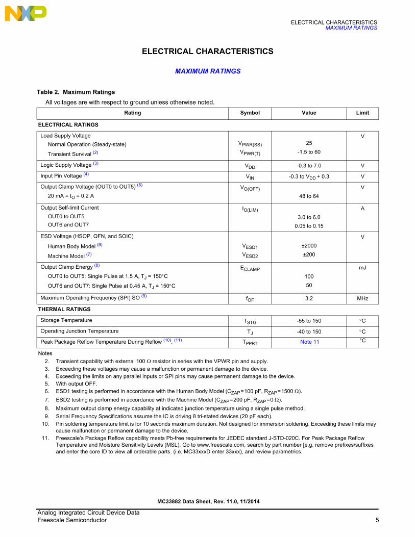
ELECTRICAL CHARACTERISTICSMAXIMUM RATINGS
ELECTRICAL CHARACTERISTICS
MAXIMUM RATINGS
Table 2. Maximum Ratings
All voltages are with respect to ground unless otherwise noted.
Rating Symbol Value Limit
ELECTRICAL RATINGS
Load Supply Voltage
Normal Operation (Steady-state)
Transient Survival (2)
VPWR(SS)
VPWR(T)
25
-1.5 to 60
V
Logic Supply Voltage (3) VDD -0.3 to 7.0 V
Input Pin Voltage (4) VIN -0.3 to VDD + 0.3 V
Output Clamp Voltage (OUT0 to OUT5) (5)
20 mA = IO = 0.2 A
VO(OFF)
48 to 64
V
Output Self-limit Current
OUT0 to OUT5
OUT6 and OUT7
IO(LIM)
3.0 to 6.0
0.05 to 0.15
A
ESD Voltage (HSOP, QFN, and SOIC)
Human Body Model (6)
Machine Model (7)
VESD1
VESD2
±2000
±200
V
Output Clamp Energy (8)
OUT0 to OUT5: Single Pulse at 1.5 A, TJ = 150C
OUT6 and OUT7: Single Pulse at 0.45 A, TJ = 150C
ECLAMP
100
50
mJ
Maximum Operating Frequency (SPI) SO (9) fOF 3.2 MHz
THERMAL RATINGS
Storage Temperature TSTG -55 to 150 C
Operating Junction Temperature TJ -40 to 150 C
Peak Package Reflow Temperature During Reflow (10), (11) TPPRT Note 11 °C
Notes
2. Transient capability with external 100 resistor in series with the VPWR pin and supply.
3. Exceeding these voltages may cause a malfunction or permanent damage to the device.4. Exceeding the limits on any parallel inputs or SPI pins may cause permanent damage to the device.5. With output OFF.6. ESD1 testing is performed in accordance with the Human Body Model (CZAP = 100 pF, RZAP = 1500 ).
7. ESD2 testing is performed in accordance with the Machine Model (CZAP = 200 pF, RZAP = 0 ).
8. Maximum output clamp energy capability at indicated junction temperature using a single pulse method.
9. Serial Frequency Specifications assume the IC is driving 8 tri-stated devices (20 pF each).
10. Pin soldering temperature limit is for 10 seconds maximum duration. Not designed for immersion soldering. Exceeding these limits may cause malfunction or permanent damage to the device.
11. Freescale’s Package Reflow capability meets Pb-free requirements for JEDEC standard J-STD-020C. For Peak Package Reflow Temperature and Moisture Sensitivity Levels (MSL), Go to www.freescale.com, search by part number [e.g. remove prefixes/suffixes and enter the core ID to view all orderable parts. (i.e. MC33xxxD enter 33xxx), and review parametrics.
MC33882 Data Sheet, Rev. 11.0, 11/2014
Analog Integrated Circuit Device DataFreescale Semiconductor 5
ELECTRICAL CHARACTERISTICSMAXIMUM RATINGS
THERMAL RESISTANCE (12), (13)
Junction-to-Ambient, Natural Convection, Single-Layer Board (1s) (14)
HSOPQFNSOIC
RJA418572
C/W
Junction-to-Ambient, Natural Convection, Four-Layer Board (2s2p) (15)
HSOPQFNSOIC(17)
RJMA1827
TBD
C/W
Junction-to-Board (Bottom)
HSOPQFNSOIC(17)
RJB
3.010
TBD
C/W
Junction-to-Case (Top) (16)
HSOPQFNSOIC
RJC
0.21.21.0
C/W
Notes12. Junction temperature is a function of on-chip power dissipation, package thermal resistance, mounting site (board) temperature, ambient
temperature, air flow, power dissipation of other components on the board, and board thermal resistance. 13. Thermal resistance between the die and the printed circuit board per JEDEC JESD51-8. Board temperature is measured on the top
surface of the board near the package.14. Per SEMI G38-87 and JEDEC JESD51-2 with the single-layer board horizontal.15. Per JEDEC JESD51-6 with the board horizontal.16. Indicates the average thermal resistance between the die and the case top surface as measured by the cold plate method (MIL SPEC
883, Method 1012.1) with the cold plate temperature used for the case temperature.17. This value will be included when available.
Table 2. Maximum Ratings (continued)
All voltages are with respect to ground unless otherwise noted.
Rating Symbol Value Limit
MC33882 Data Sheet, Rev. 11.0, 11/2014
Analog Integrated Circuit Device Data6 Freescale Semiconductor

ELECTRICAL CHARACTERISTICSSTATIC ELECTRICAL CHARACTERISTICS
STATIC ELECTRICAL CHARACTERISTICS
Table 3. Static Electrical Characteristics
Characteristics noted under conditions 4.75 V VDD 5.25 V, 9.0 V VPWR 17 V, -40 C TA 125 C, unless otherwise noted.
Characteristic Symbol Min Typ Max Unit
POWER INPUT
Supply Voltage Ranges
Functional Threshold (18)
Full Operation
Logic Supply Voltage
V PWR
V PWR
VDD
4.5
8.0
4.5
5.5
–
5.0
8.0
25
5.5
V
VPWR Supply Current (All Outputs ON) (19)
IO = 1.0 A Each
I PWR (ON)
– – 7.5
mA
Over-voltage Shutdown (20) V PWR (OV) 30 – 40 V
Over-voltage Shutdown Hysteresis (21) V PWR (OV) HYS 0.4 – 1.5 V
Power-ON Reset Threshold, VDD (22) V POR 2.5 – 3.5 V
Logic Supply Current (All Outputs ON)
VDD = 5.5 VI DD
– – 5.0
mA
POWER OUTPUT
Output Drain-to-Source ON Resistance
OUT0 to OUT5: TJ = 150°C, VPWR = 13.0 V, IO = 1.0 ARDS(ON)
– 0.6 0.8
Output Drain-to-Source ON Resistance
OUT0 to OUT5: TJ = 25°C, VPWR = 13.0 V, IO = 1.0 ARDS(ON)
– 0.4 0.6
Output Self-limiting Current
VPWR = 13.0 V, VDD = 4.5 V, VIN = 5.0 VI O (LIM)
3.0 – 6.0
A
Open Load OFF Detection (Outputs Programmed OFF) V OFF (TH) 2.5 – 3.5 V
Output OFF (Open Load Detect) Drain Current (Output Pins Programmed OFF) (23)
OUT0 to OUT5
OUT6 and OUT7
I O (OFF)
20
20
–
–
120
80
A
Output ON (Open Load Detect) Drain Current (Output Pins Programmed ON) (24)
–20 – 200
mA
Output Clamp Voltage
OUT0 to OUT5: IO = 20 mA, tCLAMP = 100 s
V OK
48 52 64
V
Output Leakage Current
VDD = VPWR = 0.5 V, VOUT = 24 VI OLK
– 1.0 10
A
Drain-to-Source Diode Forward Voltage
ISD = 1.0 mA @ 25 °C
ISD = 1.0 mA @ 125 °C
V SD
–
–
–
–
1.4
0.9
V
MC33882 Data Sheet, Rev. 11.0, 11/2014
Analog Integrated Circuit Device DataFreescale Semiconductor 7
ELECTRICAL CHARACTERISTICSSTATIC ELECTRICAL CHARACTERISTICS
DIGITAL INTERFACE
SI Logic High SIV IH 4.0 – – V
SI Logic Low SIV IL – – 2.0 V
CS and SCLK Logic High CSV IH 3.0 – – V
CS and SCLK Logic Low CSV IL – – 3.0 V
Input Logic High V IH 3.15 – – V
Input Logic Low V IL – – 1.35 V
Input Pull-down Current (25)
VIN = 1.5 V
I IN (PD)
5.0 – 25
A
Input Pull-up Current (26)
VIN = 3.5 V
I IN (PU)
-25 – -5.0
A
SO and High-state Output Voltage
IOH = -1.0 mA
V SOH
3.5 – –
V
SO and Low-state Output Voltage
IOL = 1.0 mA
V SOL
0 – 0.4
V
SO and Tri-state Leakage Current
CS = 0.7 VDD, VSO = 0.3 VDD
CS = 0.7 VDD, VSO = 0.7 VDD
I SOT
-10
–
–
–
–
10
A
Input Capacitance (27)
0 = VIN = 5.5 VC IN
– – 12
pF
SO and Tri-state Capacitance (28)
0 = VIN = 5.5 VC SOT
– – 20
pF
Notes18. Outputs of device functionally turn-on (RDS(ON) = 0.95 @125 °C). SPI / parallel inputs and power outputs are operational. Fault
detection and reporting may not be fully operational within this range.19. Value reflects all outputs ON and equally conducting 1.0 A each. VPWR = 5.5 V, CS = 5.0 V.
20. An over-voltage condition will cause any enabled outputs to latch OFF (disabled).21. This parameter is guaranteed by design; however, it is not production tested.22. For VDD less than the Power-ON Reset voltage, all outputs are disabled and the serial fault register is reset to all 0s.
23. Drain current per output with VPWR = 24 V and VLOAD = 9.0 V.
24. Drain current per output with VPWR = 13 V, VLOAD = 9.0 V.
25. Inputs SI, IN0 & IN1, IN2 & IN3, IN4 & IN5, and IN0 to IN7 incorporate active internal pull-down current sinks for noise immunity enhancement.
26. The MODE and CS inputs incorporate active internal pull-up current sources for noise immunity enhancement.27. This parameter applies to inputs SI, CS, SCLK, MODE, IN0 & IN1, IN2 & IN3, IN4 & IN5, and IN0 to IN7. It is guaranteed by design;
however, it is not production tested.28. This parameter applies to the OFF state (tri-stated) condition of SO and is guaranteed by design; however, it is not production tested.
Table 3. Static Electrical Characteristics (continued)
Characteristics noted under conditions 4.75 V VDD 5.25 V, 9.0 V VPWR 17 V, -40 C TA 125 C, unless otherwise noted.
Characteristic Symbol Min Typ Max Unit
MC33882 Data Sheet, Rev. 11.0, 11/2014
Analog Integrated Circuit Device Data8 Freescale Semiconductor

ELECTRICAL CHARACTERISTICSDYNAMIC ELECTRICAL CHARACTERISTICS
DYNAMIC ELECTRICAL CHARACTERISTICS
Table 4. Dynamic Electrical Characteristics
Characteristics noted under conditions 4.75 V VDD 5.25 V, 9.0 V VPWR 17 V, -40 C TA 125C, unless otherwise noted.
Characteristic Symbol Min Typ Max Unit
POWER OUTPUT TIMING
Output Rise Time (29) t R 1.0 – 10 s
Output Fall Time (29) tF 1.0 – 10 s
Output Turn-ON Delay Time (30) t DLY (ON) 1.0 – 10 s
Output Turn-OFF Delay Time (31) t DLY (OFF) 1.0 – 10 s
Output Short Fault Sense Time (32)
RLOAD = < 1.0 V
t SS
25 – 100
s
Output Short Fault Refresh Time (33)
RLOAD = < 1.0 V
t REF
3.0 4.5 6.0
ms
Output OFF Open Load Sense Time (34) t OS(OFF) 25 60 100 s
Output ON Open Load Sense Time (35) t OS(ON) 3.0 – 12 ms
Output Short Fault ON Duty Cycle (36) SC DC 0.42 – 3.22 %
DIGITAL INTERFACE TIMING
SCLK Clock High Time (SCLK = 3.2 MHz) (37) t SCLKH – – 141 ns
SCLK Clock Low Time (SCLK = 3.2 MHz) (37) t SCLKL – – 141 ns
Falling Edge (0.8 V) of CS to Rising Edge (2.0 V) of SCLK
Required Setup Time (37)
t LEAD
– – 140
ns
Falling Edge (0.8 V) of SCLK to Rising Edge (2.0 V) of CS
Required Setup Time (37)
t LAG
– – 50
ns
SI, CS, SCLK Incoming Signal Rise Time (37) t RSI – – 50 ns
SI, CS, SCLK Incoming Signal Fall Time (37) t FSI – – 50 ns
Notes29. Output Rise and Fall time measured at 10% to 90% and 90% to 10% voltage points respectively across 15 resistive load to a VBAT
of 15 V, VPWR = 15 V.
30. Output Turn-ON Delay Time measured from rising edge (3.0 V) VIN (CS for serial) to 90% VO using a 15 load to a VBAT of 15 V,
VPWR = 15 V.
31. Output Turn-OFF Delay Time measured from falling edge (1.0 V) VIN (3.0 V rising edge of CS for serial) to 10% VO using a 15 load
to a VBAT of 15 V, VPWR = 15 V.
32. The shorted output is turned ON during tSS to retry and check if the short has cleared. The shorted output is in current limit during tSS.
The tSS is measured from the start of current limit to the end of current limit.
33. The Short Fault Refresh Time is the waiting period between tSS retry signals. The shorted output is disabled during this refresh time.
The tREF is measured from the end of current limit to the start of current limit.
34. The tOS(OFF) is measured from the time the faulted output is turned OFF until the fault bit is available to be loaded into the internal fault
register. To guarantee a fault is reported on SO, the falling edge of CS must occur at least 100 s after the faulted output is off.35. The tOS(ON) is measured from the time the faulted output is turned ON until the fault bit is available to be loaded into the internal fault
register. To guarantee a fault is reported on SO, the falling edge of CS must occur at least 12 ms after the faulted output is ON.36. Percent Output Short Fault ON Duty Cycle is defined as (tSS) (tREF) x 100. This specification item is provided FYI and is not tested.
37. Parameter is not tested and values suggested are for system design consideration only in preventing the occurrence of double pulsing.
MC33882 Data Sheet, Rev. 11.0, 11/2014
Analog Integrated Circuit Device DataFreescale Semiconductor 9
ELECTRICAL CHARACTERISTICSDYNAMIC ELECTRICAL CHARACTERISTICS
SI Setup to Rising Edge (2.0 V) of SCLK (at 3.2 MHz)
Required Setup Time (38)
t SISU
– – 45
ns
SO Setup to SCLK Rising (2.0 V) / Falling (0.8 V) Edge
Required Setup Time (38)
t SOSU
90 – –
ns
SI Hold After Rising Edge (2.0 V) of SCLK (at 3.2 MHz)
Required Hold Time (38)
t SIHOLD
– – 45
ns
SO Hold After SCLK Rising (2.0 V) / Falling (0.8 V) Edge
Required Hold Time (38)
t SOHOLD
90 – –
ns
SO Rise Time
CL = 200 pF
t RSO
– – 50
ns
SO Fall Time
CL = 200 pF
t FSO –
– 50
ns
Falling Edge of CS (0.8 V) to SO Low-impedance (39) t SOEN – – 110 ns
Rising Edge of CS (2.0 V) to SO High-impedance (40) t SODIS – – 110 ns
Falling Edge of SCLK (0.8 V) to SO Data Valid
CL = 200 pF at 3.2 MHz (41)
t SOVALID
– 65 80
ns
CS Rising Edge to Next Falling Edge (38) Xfer DELAY – – 1.0 s
Notes38. Parameter is not tested and values suggested are for system design consideration only in preventing the occurrence of double pulsing.
39. Enable time required for SO. Pull-up resistor = 10 k.
40. Disable time required for SO. Pull-up resistor = 10 k.
41. Time required to obtain valid data out of SO following the falling edge of SCLK.
Table 4. Dynamic Electrical Characteristics (continued)
Characteristics noted under conditions 4.75 V VDD 5.25 V, 9.0 V VPWR 17 V, -40 C TA 125C, unless otherwise noted.
Characteristic Symbol Min Typ Max Unit
MC33882 Data Sheet, Rev. 11.0, 11/2014
Analog Integrated Circuit Device Data10 Freescale Semiconductor
ELECTRICAL CHARACTERISTICSTIMING DIAGRAMS
TIMING DIAGRAMS
Figure 4. Short Occurring While On, Ending During Refresh (ILOAD = 1.0 A)
GATE X = COMMAND SIGNAL AT THE GATE OF DRIVER X
FAULT BIT X = INTERNAL FAULT REGISTER BIT STATE
TREF x = FIRST REFRESH TIME MAY BE LESS THAN TREF
ILOAD = 1A
NORMAL OPERATION
INPUT X
GATE X
OUT X
FAULT BIT X FAULT FAULT
ILOAD0A
TREFTREFTREFTREF
IDLIMTSSA
ONOFF
SHORTED LOAD / SHORT - TO - VBAT
5V0V
SHORT OCCURS WHILE ON, ENDS DURING REFRESH
NPUT X
GATE X
OUT X
FAULT BIT X
IDLIMILOAD0A
ONOFF
5V0V
CSB
TSSD TSSD
Input X
Gate X
IOUT X
5.0 V0 V
ONOFF
ILOAD0 A
IO(LIM)
Fault Bit X
Shorted Load/Short-to-VPWR
tREF tREF
tSSD tSSA tSSD
tREF tREF
FaultFault
Input X
Gate X
IOUT X
5.0 V0 V
ON
ILOAD0 A
IO(LIM)
Fault Bit X
OFF
OFF
CB
Gate X = Command Signal at the Gate of Driver XFault Bit X = Internal Fault Register Bit StatetREF X = First Refresh Time may be less than tREFILOAD = 1.0 A
NormalOperation
ShortedOperation
MC33882 Data Sheet, Rev. 11.0, 11/2014
Analog Integrated Circuit Device DataFreescale Semiconductor 11
ELECTRICAL CHARACTERISTICSTIMING DIAGRAMS
Figure 5. Short Occurring While On, Ending During Retry (ILOAD = 1.0 A)
Figure 6. Short Occurring While On, Ending During Refresh (ILOAD = 20 mA)
GATE X = COMMAND SIGNAL AT THE GATE OF DRIVER X
FAULT BIT X = INTERNAL FAULT REGISTER BIT STATE
TREF x = FIRST REFRESH TIME MAY BE LESS THAN TREF
ILOAD = 1A
NORMAL OPERATION
INPUT X
GATE X
IOUT X
FAULT BIT X FAULT FAULT
ILOAD0A
TREFTREFTREFTREF
IDLIMTSSA
ONOFF
SHORTED LOAD / SHORT - TO - VBAT
5V0V
SHORT OCCURS WHILE ON, ENDS DURING RETRY
INPUT X
GATE X
IOUT X
FAULT BIT X
IDLIMILOAD0A
ONOFF
5V0V
CSB
TSSD TSSD
Gate X = Command Signal at the Gate of Driver XFault Bit X = Internal Fault Register Bit StatetREF X = First Refresh Time may be less than tREFILOAD = 1.0 A
Input X
Gate X
IOUT X
5.0 V0 V
ON
ILOAD0 A
IO(LIM)
Fault Bit X
Input X
Gate X
IOUT X
5.0 V0 V
ON
ILOAD0 A
IO(LIM)
Fault Bit X
OFF
CB
Shorted Load/Short-to-VPWR
tSSD
tREFtREF
tSSDtSSA
tREFtREF
FaultFault
ShortedOperation
NormalOperation
OFF
GATE X = COMMAND SIGNAL AT THE GATE OF DRIVER X
FAULT BIT X = INTERNAL FAULT REGISTER BIT STATE
TREF x = FIRST REFRESH TIME MAY BE LESS THAN TREF
ILOAD = 20mA
NORMAL OPERATION
INPUT X
GATE X
IOUT X
FAULT BIT X FAULT FAULT
ILOAD0A
TREFTREFTREFTREF
IDLIMTSSD
ONOFF
SHORTED LOAD / SHORT - TO - VBAT
5V0V
SHORT OCCURS WHILE ON, ENDS DURING REFRESH
INPUT X
GATE X
IOUT X
FAULT BIT X
IDLIMILOAD0A
ONOFF
5V0V
CSB
TSSA
Input X
Gate X
IOUT X
5.0 V0 V
ON
ILOAD0 A
IO(LIM)
Fault Bit X
OFF
Input X
Gate X
IOUT X
5.0 V0 V
ON
ILOAD0 A
IO(LIM)
Fault Bit X
OFF
CB
Shorted Load/Short-to-VPWR
Gate X = Command Signal at the Gate of Driver XFault Bit X = Internal Fault Register Bit StatetREF X = First Refresh Time may be less than tREFILOAD = 20 mA
Fault Fault
tREFtREF tREF tREF
tSSA tSSD
NormalOperation
ShortedOperation
MC33882 Data Sheet, Rev. 11.0, 11/2014
Analog Integrated Circuit Device Data12 Freescale Semiconductor

ELECTRICAL CHARACTERISTICSTIMING DIAGRAMS
Figure 7. Short Occurring While On, Ending During Retry (ILOAD = 20 mA)
GATE X = COMMAND SIGNAL AT THE GATE OF DRIVER X
FAULT BIT X = INTERNAL FAULT REGISTER BIT STATE
TREF x = FIRST REFRESH TIME MAY BE LESS THAN TREF
ILOAD = 20mA
NORMAL OPERATION
INPUT X
GATE X
IOUT X
FAULT BIT X FAULT FAULT
ILOAD0A
TREFTREFTREFTREF
IDLIMTSSD
ONOFF
SHORTED LOAD / SHORT - TO - VBAT
5V0V
SHORT OCCURS WHILE ON, ENDS DURING RETRY
INPUT X
GATE X
IOUT X
FAULT BIT X
IDLIMILOAD0A
ONOFF
5V0V
CSB
TSSDTSSA
Gate X = Command Signal at the Gate of Driver XFault Bit X = Internal Fault Register Bit StatetREF X = First Refresh Time may be less than tREFILOAD = 20 mA
Input X
Gate X
IOUT X
5.0 V0 V
ON
ILOAD0 A
IO(LIM)
Fault Bit X
OFF
CB
Input X
Gate X
IOUT X
5.0 V0 V
ON
ILOAD0 A
IO(LIM)
Fault Bit X
OFF
Fault Fault
tREFtREFtREFtREF
tSSA tSSD tSSD
Shorted Load/Short-to-VPWR
ShortedOperation
NormalOperation
MC33882 Data Sheet, Rev. 11.0, 11/2014
Analog Integrated Circuit Device DataFreescale Semiconductor 13
ELECTRICAL CHARACTERISTICSELECTRICAL PERFORMANCE CURVES
ELECTRICAL PERFORMANCE CURVES
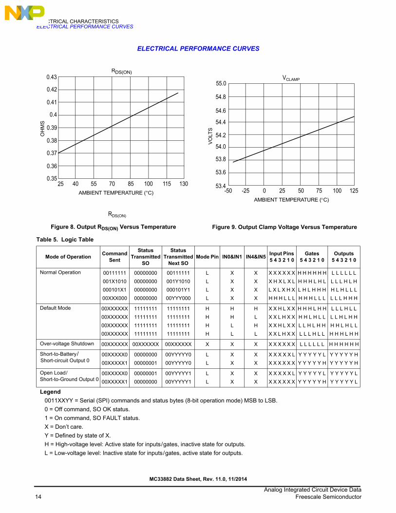
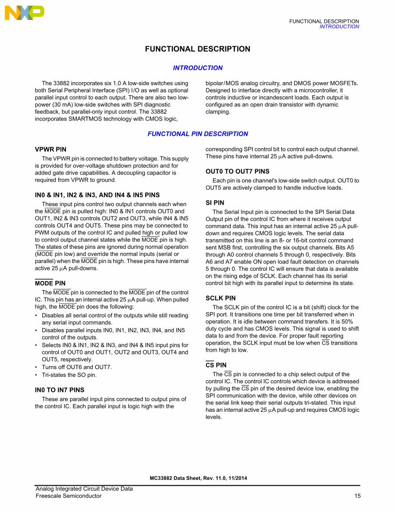
Figure 8. Output RDS(ON) Versus Temperature Figure 9. Output Clamp Voltage Versus Temperature
0.37
0.38
AMBIENT TEMPERATURE (°C)
OH
MS
55 70 11540 85 100 130
0.39
0.4
0.41
0.42
0.36
0.35
0.43
RDS(ON)
RDS(ON)
25
AMBIENT TEMPERATURE (C)
VO
LTS
-50 0 25 100-25 50 75 125
53.8
54.0
54.2
54.4
54.6
54.8
53.6
53.4
55.0VCLAMP
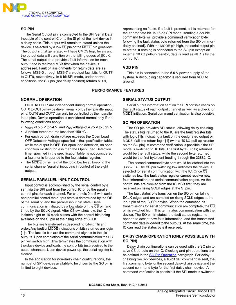
Table 5. Logic Table
Mode of OperationCommand
Sent
Status Transmitted
SO
Status Transmitted
Next SOMode Pin IN0&IN1 IN4&IN5
Input Pins 5 4 3 2 1 0
Gates5 4 3 2 1 0
Outputs5 4 3 2 1 0
Normal Operation 00111111
001X1010
000101X1
00XXX000
00000000
00000000
00000000
00000000
00111111
001Y1010
000101Y1
00YYY000
L
L
L
L
X
X
X
X
X
X
X
X
X X X X X X
X H X L X L
L X L X H X
H H H L L L
H H H H H H
H H H L H L
L H L H H H
H H H L L L
L L L L L L
L L L H L H
H L H L L L
L L L H H H
Default Mode 00XXXXXX
00XXXXXX
00XXXXXX
00XXXXXX
11111111
11111111
11111111
11111111
11111111
11111111
11111111
11111111
H
H
H
H
H
H
L
L
H
L
H
L
X X H L X X
X X L H X X
X X H L X X
X X L H X X
H H H L H H
H H L H L L
L L H L H H
L L L H L L
L L L H L L
L L H L H H
H H L H L L
H H H L H H
Over-voltage Shutdown 00XXXXXX 00XXXXXX 00XXXXXX X X X X X X X X X L L L L L L H H H H H H
Short-to-Battery / Short-circuit Output 0
00XXXXX0
00XXXXX1
00000000
00000001
00YYYYY0
00YYYYY0
L
L
X
X
X
X
X X X X X L
X X X X X X
Y Y Y Y Y L
Y Y Y Y Y H
Y Y Y Y Y H
Y Y Y Y Y H
Open Load / Short-to-Ground Output 0
00XXXXX0
00XXXXX1
00000001
00000000
00YYYYY1
00YYYYY1
L
L
X
X
X
X
X X X X X L
X X X X X X
Y Y Y Y Y L
Y Y Y Y Y H
Y Y Y Y Y L
Y Y Y Y Y L
Legend
0011XXYY = Serial (SPI) commands and status bytes (8-bit operation mode) MSB to LSB.
0 = Off command, SO OK status.
1 = On command, SO FAULT status.
X = Don’t care.
Y = Defined by state of X.
H = High-voltage level: Active state for inputs / gates, inactive state for outputs.
L = Low-voltage level: Inactive state for inputs / gates, active state for outputs.
MC33882 Data Sheet, Rev. 11.0, 11/2014
Analog Integrated Circuit Device Data14 Freescale Semiconductor
FUNCTIONAL DESCRIPTIONINTRODUCTION
FUNCTIONAL DESCRIPTION
INTRODUCTION
The 33882 incorporates six 1.0 A low-side switches using both Serial Peripheral Interface (SPI) I /O as well as optional parallel input control to each output. There are also two low-power (30 mA) low-side switches with SPI diagnostic feedback, but parallel-only input control. The 33882 incorporates SMARTMOS technology with CMOS logic,
bipolar / MOS analog circuitry, and DMOS power MOSFETs. Designed to interface directly with a microcontroller, it controls inductive or incandescent loads. Each output is configured as an open drain transistor with dynamic clamping.
FUNCTIONAL PIN DESCRIPTION
VPWR PINThe VPWR pin is connected to battery voltage. This supply
is provided for over-voltage shutdown protection and for added gate drive capabilities. A decoupling capacitor is required from VPWR to ground.
IN0 & IN1, IN2 & IN3, AND IN4 & IN5 PINSThese input pins control two output channels each when
the MODE pin is pulled high: IN0 & IN1 controls OUT0 and OUT1, IN2 & IN3 controls OUT2 and OUT3, while IN4 & IN5 controls OUT4 and OUT5. These pins may be connected to PWM outputs of the control IC and pulled high or pulled low to control output channel states while the MODE pin is high. The states of these pins are ignored during normal operation (MODE pin low) and override the normal inputs (serial or parallel) when the MODE pin is high. These pins have internal active 25 A pull-downs.
MODE PINThe MODE pin is connected to the MODE pin of the control
IC. This pin has an internal active 25 A pull-up. When pulled high, the MODE pin does the following:
• Disables all serial control of the outputs while still reading any serial input commands.
• Disables parallel inputs IN0, IN1, IN2, IN3, IN4, and IN5 control of the outputs.
• Selects IN0 & IN1, IN2 & IN3, and IN4 & IN5 input pins for control of OUT0 and OUT1, OUT2 and OUT3, OUT4 and OUT5, respectively.
• Turns off OUT6 and OUT7.• Tri-states the SO pin.
IN0 TO IN7 PINSThese are parallel input pins connected to output pins of
the control IC. Each parallel input is logic high with the
corresponding SPI control bit to control each output channel. These pins have internal 25 A active pull-downs.
OUT0 TO OUT7 PINSEach pin is one channel's low-side switch output. OUT0 to
OUT5 are actively clamped to handle inductive loads.
SI PINThe Serial Input pin is connected to the SPI Serial Data
Output pin of the control IC from where it receives output command data. This input has an internal active 25 A pull-down and requires CMOS logic levels. The serial data transmitted on this line is an 8- or 16-bit control command sent MSB first, controlling the six output channels. Bits A5 through A0 control channels 5 through 0, respectively. Bits A6 and A7 enable ON open load fault detection on channels 5 through 0. The control IC will ensure that data is available on the rising edge of SCLK. Each channel has its serial control bit high with its parallel input to determine its state.
SCLK PINThe SCLK pin of the control IC is a bit (shift) clock for the
SPI port. It transitions one time per bit transferred when in operation. It is idle between command transfers. It is 50% duty cycle and has CMOS levels. This signal is used to shift data to and from the device. For proper fault reporting operation, the SCLK input must be low when CS transitions from high to low.
CS PINThe CS pin is connected to a chip select output of the
control IC. The control IC controls which device is addressed by pulling the CS pin of the desired device low, enabling the SPI communication with the device, while other devices on the serial link keep their serial outputs tri-stated. This input has an internal active 25 A pull-up and requires CMOS logic levels.
MC33882 Data Sheet, Rev. 11.0, 11/2014
Analog Integrated Circuit Device DataFreescale Semiconductor 15
FUNCTIONAL DESCRIPTIONFUNCTIONAL PIN DESCRIPTION
SO PINThe Serial Output pin is connected to the SPI Serial Data
Input pin of the control IC or to the SI pin of the next device in a daisy chain. This output will remain tri-stated unless the device is selected by a low CS pin or the MODE pin goes low. The output signal generated will have CMOS logic levels and the output data will transition on the falling edges of SCLK. The serial output data provides fault information for each output and is returned MSB first when the device is addressed. Fault bit assignments for return data are as follows: MSB-0 through MSB-7 are output fault bits for OUT7 to OUT0, respectively. In 8-bit SPI mode, under normal conditions, the SO pin (not daisy chained) returns all 0s,
representing no faults. If a fault is present, a 1 is returned for the appropriate bit. In 16-bit SPI mode, sending a double command byte will provide a command verification byte following the fault status byte returned from the SO pin (non-daisy chained). With the MODE pin high, the serial output pin tri-states. If nothing is connected to the SO pin except an external 10 k pull-up resistor, data is read as all [1]s by the control IC.
VDD PINThis pin is connected to the 5.0 V power supply of the
system. A decoupling capacitor is required from VDD to ground.
PERFORMANCE FEATURES
NORMAL OPERATIONOUT0 to OUT7 are independent during normal operation.
OUT0 to OUT5 may be driven serially or by their parallel input pins. OUT6 and OUT7 can only be controlled by their parallel input pins. Device operation is considered normal only if the following conditions apply:
• VPWR of 5.5 V to 24 V, and VDD voltage of 4.75 V to 5.25 V.• Junction temperatures less than 150 C.• For each output, drain voltage exceeds the Open Load
OFF Detection Voltage, specified in the specification table, while the output is OFF. For open load detection, an open condition existing for less than the Open Load Detection time, specified in the specification table, is not considered a fault nor is it reported to the fault status register.
• The MODE pin is held at the logic low level, keeping the serial channel / parallel input pins in control of the eight outputs.
SERIAL / PARALLEL INPUT CONTROLInput control is accomplished by the serial control byte
sent via the SPI port from the control IC or by the parallel control pins for each channel. For channels 0 to 5 with serial and parallel control the output state is determined by the OR of the serial bit and the parallel input pin state. Serial communication is initiated by a low state on the CS pin and timed by the SCLK signal. After CS switches low, the IC initiates eight or 16 clock pulses with the control bits being available on the SI pin at the rising edge of SCLK.
The bits are transferred in descending bit-significant order. Any fault or MODE indications on bits returned are logic [1]s. The last six bits are the command signals to the six outputs. Upon completion of the serial communication the CS pin will switch high. This terminates the communication with the slave device and loads the control bits just received to the output channels. Upon device power-up, the serial register is cleared.
In the application for non-daisy chain configurations, the number of SPI devices available to be driven by the SO pin is limited to eight devices.
SERIAL STATUS OUTPUTSerial output information sent on the SPI port is a check on
the fault status of each output channel as well as a check for MODE initiation. Serial command verification is also possible.
SO PIN OPERATIONThe SO pin provides SPI status, allowing daisy chaining.
The status bits returned to the IC are the fault register bits with logic [1]s indicating a fault on the designated output or MODE if all bits return logic [1] (with a 10 k pull-up resistor on the SO pin). A command verification is possible if the SPI mode is switched to 16 bits. The first byte (8 bits) returned would be the fault status, while the second byte returned would be the first byte sent feeding through the 33882 IC.
The second command byte sent would be latched into the 33882 IC. The CS pin switching low indicates the device is selected for serial communication with the IC. Once CS switches low, the fault status register cannot receive new fault information and serial communication begins. As the control bits are clocked from the IC MSB first, they are received on rising SCLK edges at the SI pin.
The fault status bits transition on the SO pin on falling SCLK edges and are sampled on rising SCLK edges at the input pin of the IC SPI device. When the command bit transmissions for serial communication are complete, the CS pin is switched high. This terminates communication with the device. The SO pin tri-states, the fault status register is opened to accept new fault information, and the transmitted command data is loaded to the outputs. At the same time, the IC can read the status byte it received.
DAISY CHAIN OPERATION (ONLY POSSIBLE WITH SO PIN)
Daisy chain configurations can be used with the SO pin to save CS outputs on the IC. Clocking and pin operations are as defined in the SO Pin Operation paragraph. For daisy chaining two 8-bit devices, a 16-bit SPI command is sent, the first command byte for the second daisy chain device and the second command byte for the first daisy chain device. A command verification is possible if the SPI mode is switched
MC33882 Data Sheet, Rev. 11.0, 11/2014
Analog Integrated Circuit Device Data16 Freescale Semiconductor
FUNCTIONAL DESCRIPTIONFUNCTIONAL PIN DESCRIPTION
to 32 bits. The first word sent is command verification data fed through the two 33882 ICs. Data returned in the 32 bits is the two fault status bytes, followed by the first word sent. Bits sent out are sampled on rising SCLK edges at the input pin of the next IC in the daisy chain.
Note Because SO pins of the 33882 ICs are tri-stated, any device receiving its SPI data from a previous 33882 IC SO pin in a daisy chain will not receive data if the MODE pin is low. This prohibits setting SPI-controlled channels ON with a SPI command while the MODE pin is low. Therefore, all channels remain OFF when the MODE pin changes from low to high at vehicle power-up.
MODE OPERATIONDuring normal operation output channels are controlled by
either the Serial Input control bits or the parallel input pins. If the MODE pin is pulled high:
• Serial input control is disabled.• Parallel input pins IN0 to IN5 are ignored.• The SO pin is tri-stated.
OUT0 and OUT1, OUT2 and OUT3, and OUT4 and OUT5 are controlled by the IN0 & IN1, IN2 & IN3, and IN4 & IN5 pins, respectively. When a 10 kpull-up resistor is used, a logic high on the MODE pin or an open serial output pin is flagged by the SPI when all bits are returned as logic [1]s.
Although a logic high on the MODE pin disables serial control of outputs, data can still be clocked into the serial input register. This allows programming of a desired state for the outputs taking effect only when the MODE pin returns to a logic low. For applications using the SO pin, daisy chaining is permitted, but if the MODE pin is high, writing to other than the first IC in a daisy chain is not possible because the serial outputs are tri-stated.
OUTPUT DRIVERSThe high power OUT0 to OUT5 outputs are active
clamped, low-side switches driving 1.0 A typical or less loads. The low-power OUT6 and OUT7 outputs are unclamped low-side switches driving 30 mA typical or less loads. All outputs are individually protected from short circuit or short-to-battery conditions and transient voltages. The outputs are also protected by short-circuit device shutdown. Each output individually detects and reports open load /short-to-ground and short-circuit /short-to-battery faults.
FAULT SENSE / PROTECTION CIRCUITRYEach output channel individually detects shorted loads /
short-to-battery while the output is ON and open load /short-to-ground while the output is OFF. OUT0 to OUT5 may also be programmed via SPI bits 6 and 7 to detect open loads and shorts-to-ground while the output is ON. Whenever a short or open fault condition is present on a particular output channel, its fault bit in the internal fault register indicates the fault with a logic [1].
When a fault ends, its fault bit remains set until the SPI register is read, then it returns to a logic [0], indicating a
normal condition. When the CS pin is pulled low for serial communication, the fault bits in the internal fault register latch, preventing erroneous status transmissions and the forthcoming communication reports this latched fault status. The SO pin serial output data for 8-bit SPI mode are the fault status register bits.
For 16-bit SPI mode and SO pin (non-daisy chained) use, a transmitted double command provides the fault byte followed by the first byte of the double command, becoming a command verification. The status is sent back to the IC for fault monitoring. Diagnostic interpretation of the following fault types can be accomplished using the procedure described in the paragraph entitled Extensive Fault Diagnostics:
• Communication error• Open load /short-to-ground• Short-to-battery or short-circuit
When serial communication is ended, the CS pin returns high, opening the fault status register to new fault information and tri-stating the SO pin.
Two fault conditions initiate protective action by the device:
• A short-circuit or short-to-battery on a particular output will cause that output to go into a low duty cycle operation until the fault condition is removed or the input to that channel turns OFF.
• A short-circuit condition causes all channels to shut down, ignoring serial and parallel inputs to the device.
To be detected and reported as a fault, a fault condition must last a specified time (fault sense time or fault mask time). This prevents any normal switching transients from causing inadvertent fault status indications.
Fault status information should be ignored for VBAT levels outside the 9.0 V to 17 V range. The fault reporting may appear to function properly but may not be 100 percent reliable.
SHORT-CIRCUIT /SHORT-TO-BATTERY SENSING AND PROTECTION
When an output is turned ON, if the drain current limit is reached, the current remains at the limit until the short-circuit sense time, tSS, has elapsed. At this time, the affected output will shut down and its fault status bit switches to a logic [1]. The output goes into a low duty cycle operation as long as the short-circuit condition exists and the input to that channel is ON.
This duty cycle is defined by the sense and refresh times. If a short occurs after the output is ON, the fault sense time indicates the fault and enters the low duty cycle mode at much less than t SS. The duty cycle is low enough to keep the driver from exceeding its thermal capabilities. When the short is removed, the driver resumes normal operation at the next retry, but the fault status bit does not return to a normal logic [0] state until it is read from the SPI. When the CS pin of this device is pulled low, the fault status bits are latched, after which any new fault information is not a part of this serial communication event.
MC33882 Data Sheet, Rev. 11.0, 11/2014
Analog Integrated Circuit Device DataFreescale Semiconductor 17
FUNCTIONAL DESCRIPTIONFUNCTIONAL PIN DESCRIPTION
The low duty cycle operation for a short-circuit condition is required to protect the output. It is possible to override this duty cycle if the input signal (parallel or SPI) turns the channel ON and OFF faster than 10 kHz. For this reason control signals should not exceed this frequency.
OPEN LOAD / SHORT-TO-GROUND WHILE OFF SENSING
If the drain voltage falls below the Open Load OFF Detection Voltage at turn OFF for a period of time exceeding the Open Load Sense Time, the fault status bit for this output switches to a logic [1].
If a drain voltage falls below the Open Load OFF Detection Voltage threshold when the output has been OFF, a fault is indicated with a delay much less than the Open Load Sense Time. When the fault is removed, normal operation resumes and the fault status bit will return to a normal logic [0] state. When the CS pin of this device is pulled low, the fault status bits are latched, after which any new fault information is not part of this serial communication event.
OVER-VOLTAGE SENSING AND PROTECTIONWhen VPWR exceeds the Over-voltage Shutdown
Threshold, all channels are shut down. Serial input data and parallel inputs are ignored. The device resumes normal operation when the VPWR voltage drops below the Over-voltage Shutdown Hysteresis voltage. During over-voltage shutdown, some faults may appear to report accurately; however, fault sensing operation is only guaranteed for battery voltage levels from 9.0 V to 17 V.
FAULT STATUS MONITORING REQUIREMENTS FOR SERIALLY CONTROLLED OUTPUTS, SO PIN
Fault monitoring over the serial channel by the IC requires a minimal amount of overhead for normal operation. Each status byte received consists of all logic [0]s when faults are not present. If any logic [1]s are returned, a communication error occurred, an output fault occurred, or the MODE pin has been set low. Upon receiving any logic [1] bits, the IC must resend the last command, verifying the returned logic [1]s, or correct any communication error.
A 16-bit SPI transmission with a double command byte to this 8-bit device allows verification of the command (second byte returned) in addition to the fault byte (first byte returned). The command (second) byte returned should mirror the bits sent unless a communication error occurred, in which case the command resent should accomplish the correction.
If the returned logic [1] validates, it may indicate a MODE pin high or a confirmed output fault. If it was a confirmed output fault, extensive diagnostics could be performed, determining the fault type, especially if vehicle service is being performed. If all bits return high and verify such, the IC must verify sending a logic low to the MODE pin. It should then resend the command, verifying the MODE pin is at a logic low level, allowing resumption of a normal operation. If
all logic [1]s are again returned, there is an open SO line, an open MODE line, or the SPI is not functioning.
If the fault does not verify on the command resend, normal operation is resumed. The error could be a communication mistake, a momentary output fault, or a fault condition no longer sensed due to switching the state of the output. For the first two cases, normal operation is resumed and the software continues its normal functions. However in the third case, additional commands are required for extensive diagnosis of the fault type, if this information is mandatory.
EXTENSIVE FAULT DIAGNOSTICSMore extensive diagnosis may be required under the
following conditions:
• When the fault type of a confirmed fault is desired, the following scenarios are possible:
– If MSB-2 to MSB-7 indicates a fault, it is an open load / short-to-ground fault if the output is OFF when the fault is reported because only open load / short-to-ground sensing remains operable while an output is OFF.
– If the output is ON when the fault is reported, the fault is a short-circuit /short-to-battery if ON open load detection is not enabled via SPI. If ON open load detection is enabled, it must be disabled and the fault status reread. If the fault remains, it is a short-circuit / short-to-battery or it is an open load /short-to-ground.
– If MSB-0 to MSB-2 indicates a fault, it is an open load / short-to-ground fault if the output is OFF when the fault is reported because only open load /short-to-ground sensing remains operable while an output is OFF.
– If the output is ON when the fault is reported, the fault is a short-circuit /short-to-battery.
• When a fault did not confirm on resend, the fault could either be an short-circuit /short-to-battery fault, not sensed when turned OFF; an open load /short-to-ground fault, not sensed when turned ON; or a corrected communication error. To determine if it is an output fault condition, the faulted output must be turned back to its previous state with a new command. This command should be sent twice to read the status after the output is latched in this state, thus confirming the fault and reporting it again.
Parallel control of outputs is a mode of control, potentially requiring extensive diagnostics if a fault is reported. This is because parallel control signals are completely asynchronous to the serial commands. Status reports for parallel controlled outputs could require additional information exchange in software to:
• Avoid status reads when outputs are transitioned, thereby avoiding fault masking times.
• Obtain the state of a faulted output for determining fault type (if required).
MC33882 Data Sheet, Rev. 11.0, 11/2014
Analog Integrated Circuit Device Data18 Freescale Semiconductor
FUNCTIONAL DESCRIPTIONFUNCTIONAL PIN DESCRIPTION
SYSTEM ACTUATOR ELECTRICAL CHARACTERISTICS (AT ROOM TEMPERATURE)
All drains should have a 0.01 F filter capacitor connected to ground. Any unused output pin should not be energized. A 20 resistor to the battery is required to prevent false open load reporting. There must also be a maximum of 100 of resistance from VPWR to ground, keeping battery-powered loads OFF when the IC is powered down. However, all loads should be powered by VPWR to protect the device from full transient voltages on the battery voltage.
POWER-UPThe device is insensitive to power sequencing for VPWR
and VDD, as well as intolerant to latch-up on all I /O pins. Upon power-up, an internal power-ON reset clears the serial registers, allowing all outputs to power up in the off-state when parallel control pins are also low. Although the serial register is cleared by this power-ON reset, software must still initialize the outputs with an SPI command prior to changing the MODE pin from a high to a low state. This assures known output states when MODE is low.
MC33882 Data Sheet, Rev. 11.0, 11/2014
Analog Integrated Circuit Device DataFreescale Semiconductor 19
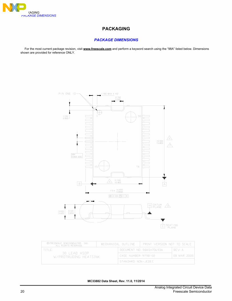
PACKAGINGPACKAGE DIMENSIONS
PACKAGING
PACKAGE DIMENSIONS
For the most current package revision, visit www.freescale.com and perform a keyword search using the “98A” listed below. Dimensions shown are provided for reference ONLY.
MC33882 Data Sheet, Rev. 11.0, 11/2014
Analog Integrated Circuit Device Data20 Freescale Semiconductor

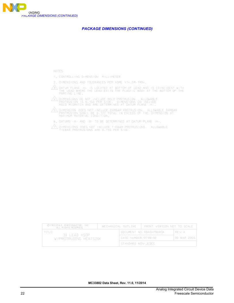
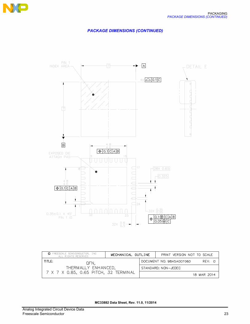
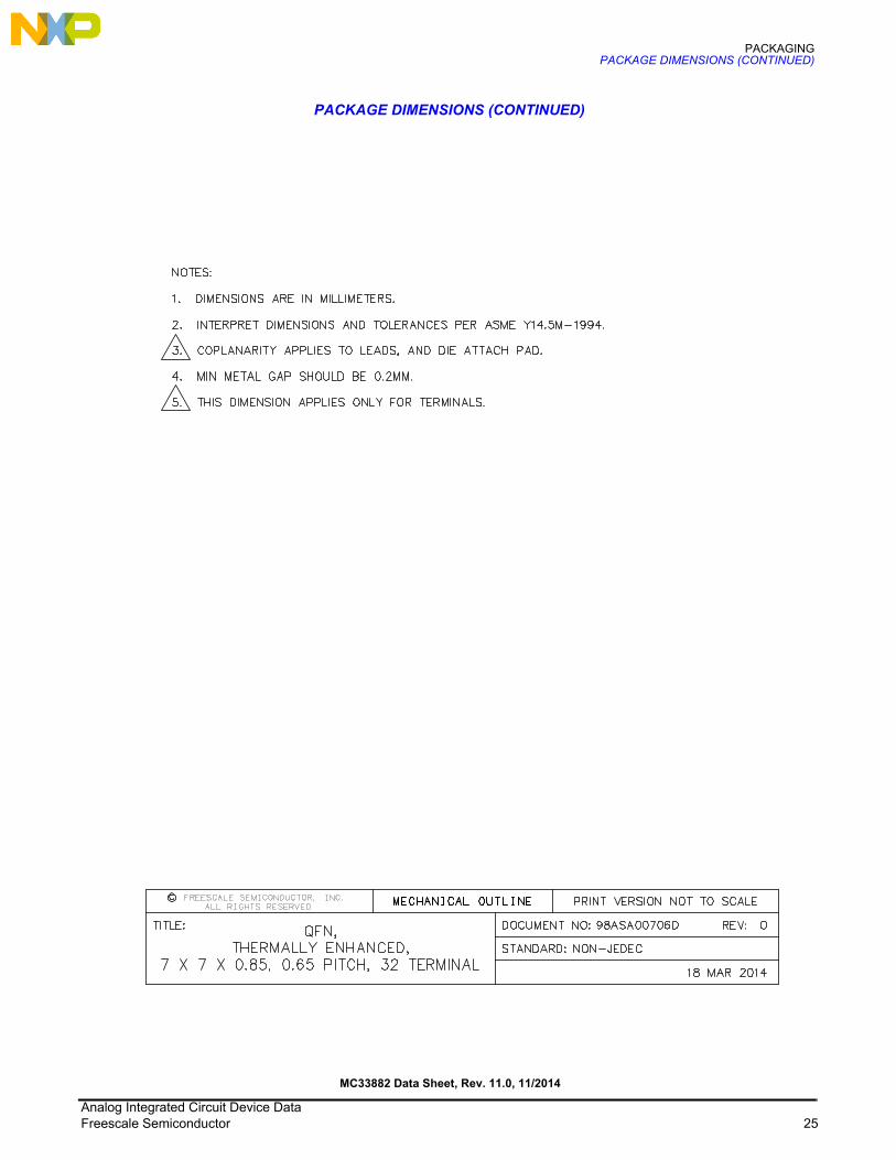
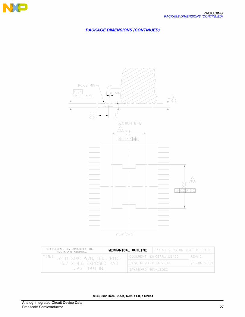
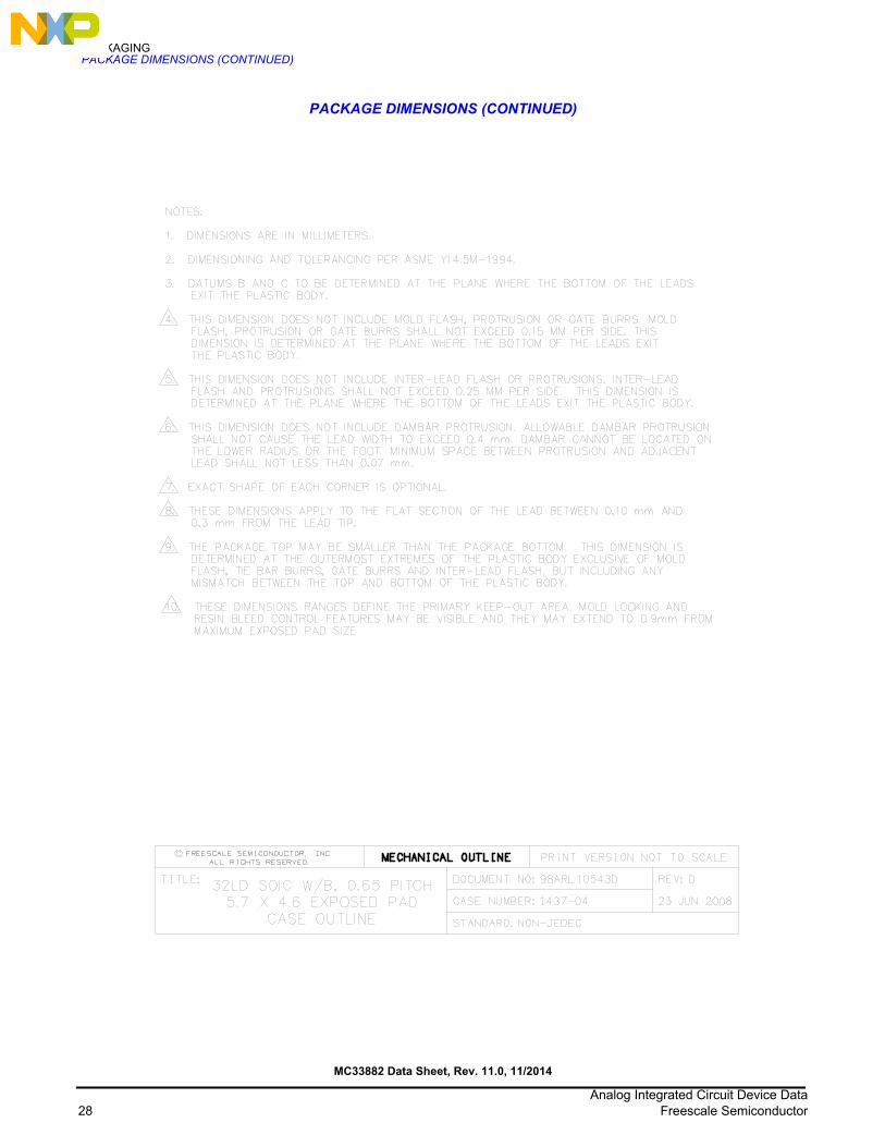
PACKAGINGPACKAGE DIMENSIONS (CONTINUED)
PACKAGE DIMENSIONS (CONTINUED)
MC33882 Data Sheet, Rev. 11.0, 11/2014
Analog Integrated Circuit Device DataFreescale Semiconductor 21
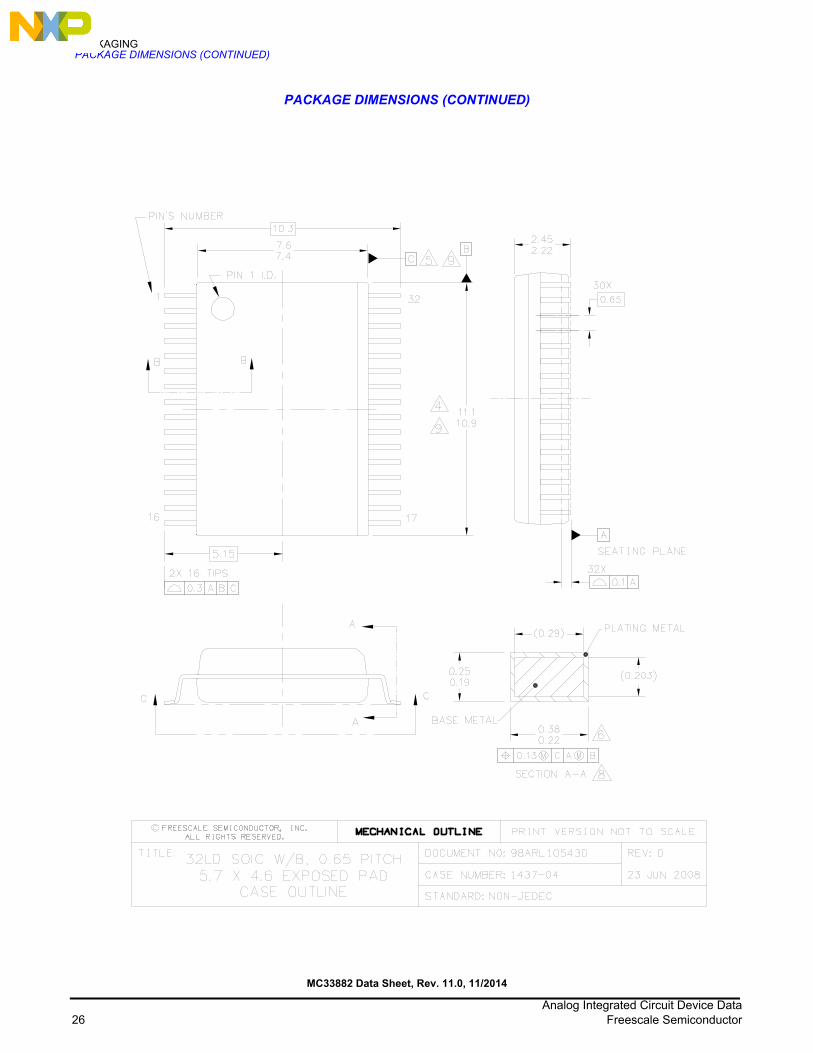
PACKAGINGPACKAGE DIMENSIONS (CONTINUED)
PACKAGE DIMENSIONS (CONTINUED)
MC33882 Data Sheet, Rev. 11.0, 11/2014
Analog Integrated Circuit Device Data22 Freescale Semiconductor
PACKAGINGPACKAGE DIMENSIONS (CONTINUED)
PACKAGE DIMENSIONS (CONTINUED)
MC33882 Data Sheet, Rev. 11.0, 11/2014
Analog Integrated Circuit Device DataFreescale Semiconductor 23
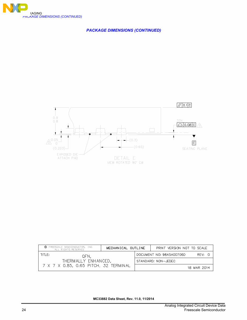
PACKAGINGPACKAGE DIMENSIONS (CONTINUED)
PACKAGE DIMENSIONS (CONTINUED)
MC33882 Data Sheet, Rev. 11.0, 11/2014
Analog Integrated Circuit Device Data24 Freescale Semiconductor
PACKAGINGPACKAGE DIMENSIONS (CONTINUED)
PACKAGE DIMENSIONS (CONTINUED)
MC33882 Data Sheet, Rev. 11.0, 11/2014
Analog Integrated Circuit Device DataFreescale Semiconductor 25
PACKAGINGPACKAGE DIMENSIONS (CONTINUED)
PACKAGE DIMENSIONS (CONTINUED)
MC33882 Data Sheet, Rev. 11.0, 11/2014
Analog Integrated Circuit Device Data26 Freescale Semiconductor
PACKAGINGPACKAGE DIMENSIONS (CONTINUED)
PACKAGE DIMENSIONS (CONTINUED)
MC33882 Data Sheet, Rev. 11.0, 11/2014
Analog Integrated Circuit Device DataFreescale Semiconductor 27
PACKAGINGPACKAGE DIMENSIONS (CONTINUED)
PACKAGE DIMENSIONS (CONTINUED)
MC33882 Data Sheet, Rev. 11.0, 11/2014
Analog Integrated Circuit Device Data28 Freescale Semiconductor
REVISION HISTORYPACKAGE DIMENSIONS (CONTINUED)
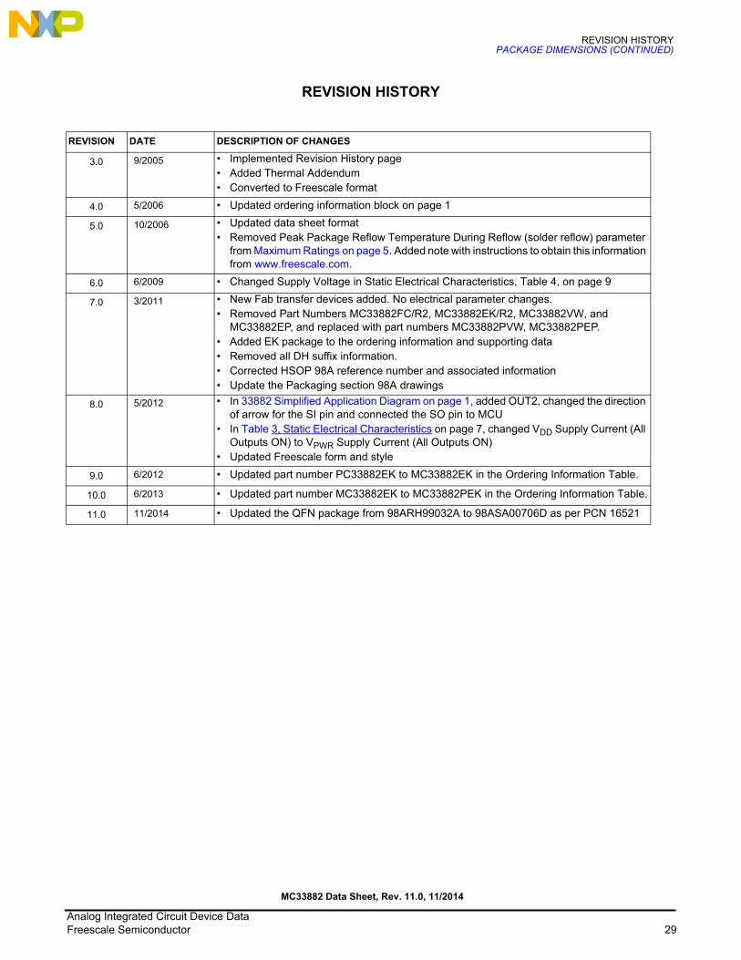
REVISION HISTORY
REVISION DATE DESCRIPTION OF CHANGES
3.0 9/2005 • Implemented Revision History page• Added Thermal Addendum• Converted to Freescale format
4.0 5/2006 • Updated ordering information block on page 1
5.0 10/2006 • Updated data sheet format• Removed Peak Package Reflow Temperature During Reflow (solder reflow) parameter
from Maximum Ratings on page 5. Added note with instructions to obtain this information from www.freescale.com.
6.0 6/2009 • Changed Supply Voltage in Static Electrical Characteristics, Table 4, on page 9
7.0 3/2011 • New Fab transfer devices added. No electrical parameter changes.• Removed Part Numbers MC33882FC/R2, MC33882EK/R2, MC33882VW, and
MC33882EP, and replaced with part numbers MC33882PVW, MC33882PEP.• Added EK package to the ordering information and supporting data• Removed all DH suffix information.• Corrected HSOP 98A reference number and associated information• Update the Packaging section 98A drawings
8.0 5/2012 • In 33882 Simplified Application Diagram on page 1, added OUT2, changed the direction of arrow for the SI pin and connected the SO pin to MCU
• In Table 3, Static Electrical Characteristics on page 7, changed VDD Supply Current (All Outputs ON) to VPWR Supply Current (All Outputs ON)
• Updated Freescale form and style
9.0 6/2012 • Updated part number PC33882EK to MC33882EK in the Ordering Information Table.
10.0 6/2013 • Updated part number MC33882EK to MC33882PEK in the Ordering Information Table.
11.0 11/2014 • Updated the QFN package from 98ARH99032A to 98ASA00706D as per PCN 16521
MC33882 Data Sheet, Rev. 11.0, 11/2014
Analog Integrated Circuit Device DataFreescale Semiconductor 29
Document Number: MC33882Rev. 11.0
11/2014
Information in this document is provided solely to enable system and software implementers to use Freescale products.
There are no express or implied copyright licenses granted hereunder to design or fabricate any integrated circuits based
on the information in this document.
Freescale reserves the right to make changes without further notice to any products herein. Freescale makes no
warranty, representation, or guarantee regarding the suitability of its products for any particular purpose, nor does
Freescale assume any liability arising out of the application or use of any product or circuit, and specifically disclaims any
and all liability, including without limitation consequential or incidental damages. “Typical” parameters that may be
provided in Freescale data sheets and/or specifications can and do vary in different applications, and actual performance
may vary over time. All operating parameters, including “typicals,” must be validated for each customer application by
customer’s technical experts. Freescale does not convey any license under its patent rights nor the rights of others.
Freescale sells products pursuant to standard terms and conditions of sale, which can be found at the following address:
freescale.com/SalesTermsandConditions.
Freescale and the Freescale logo are trademarks of Freescale Semiconductor, Inc., Reg. U.S. Pat. & Tm. Off.
SMARTMOS is a trademark of Freescale Semiconductor, Inc. All other product or service names are the property of their
respective owners.
© 2014 Freescale Semiconductor, Inc.
How to Reach Us:
Home Page: freescale.com
Web Support: freescale.com/support