max98372 diital inpt class d ampliier ith dt an bronot ... featuring dynamic headroom tracking (dht)...
TRANSCRIPT
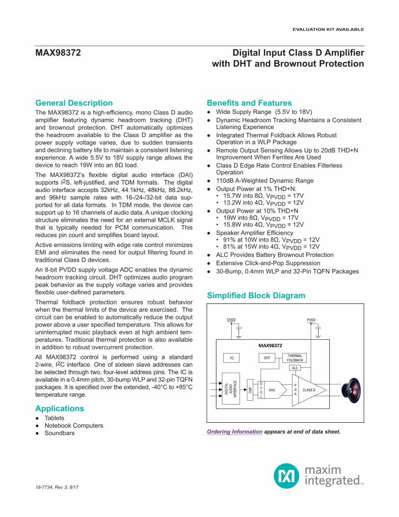
General DescriptionThe MAX98372 is a high-efficiency, mono Class D audio amplifier featuring dynamic headroom tracking (DHT) and brownout protection. DHT automatically optimizes the headroom available to the Class D amplifier as the power supply voltage varies, due to sudden transients and declining battery life to maintain a consistent listening experience. A wide 5.5V to 18V supply range allows the device to reach 19W into an 8Ω load.The MAX98372’s flexible digital audio interface (DAI) supports I2S, left-justified, and TDM formats. The digital audio interface accepts 32kHz, 44.1kHz, 48kHz, 88.2kHz, and 96kHz sample rates with 16-/24-/32-bit data sup-ported for all data formats. In TDM mode, the device can support up to 16 channels of audio data. A unique clocking structure eliminates the need for an external MCLK signal that is typically needed for PCM communication. This reduces pin count and simplifies board layout.Active emissions limiting with edge rate control minimizes EMI and eliminates the need for output filtering found in traditional Class D devices. An 8-bit PVDD supply voltage ADC enables the dynamic headroom tracking circuit. DHT optimizes audio program peak behavior as the supply voltage varies and provides flexible user-defined parameters.Thermal foldback protection ensures robust behavior when the thermal limits of the device are exercised. The circuit can be enabled to automatically reduce the output power above a user specified temperature. This allows for uninterrupted music playback even at high ambient tem-peratures. Traditional thermal protection is also available in addition to robust overcurrent protection.All MAX98372 control is performed using a standard 2-wire, I2C interface. One of sixteen slave addresses can be selected through two, four-level address pins. The IC is available in a 0.4mm pitch, 30-bump WLP and 32-pin TQFN packages. It is specified over the extended, -40°C to +85°C temperature range.
Applications Tablets Notebook Computers Soundbars
Benefits and Features Wide Supply Range (5.5V to 18V) Dynamic Headroom Tracking Maintains a Consistent
Listening Experience Integrated Thermal Foldback Allows Robust
Operation in a WLP Package Remote Output Sensing Allows Up to 20dB THD+N
Improvement When Ferrites Are Used Class D Edge Rate Control Enables Filterless
Operation 110dB A-Weighted Dynamic Range Output Power at 1% THD+N:
• 15.7W into 8Ω, VPVDD = 17V• 13.2W into 4Ω, VPVDD = 12V
Output Power at 10% THD+N• 19W into 8Ω, VPVDD = 17V• 15.8W into 4Ω, VPVDD = 12V
Speaker Amplifier Efficiency• 91% at 10W into 8Ω, VPVDD = 12V• 81% at 15W into 4Ω, VPVDD = 12V
ALC Provides Battery Brownout Protection Extensive Click-and-Pop Suppression 30-Bump, 0.4mm WLP and 32-Pin TQFN Packages
19-7734; Rev 3; 8/17
Ordering Information appears at end of data sheet.
DVDD
I2C
DIGI
TAL
AUDI
O IN
TERF
ACE
DAC CLASS D
MAX98372
DVOL
DHT
PVDD
THERMALFOLDBACK
DSP P
GA
ALC
Simplified Block Diagram
MAX98372 Digital Input Class D Amplifier with DHT and Brownout Protection
EVALUATION KIT AVAILABLE

www.maximintegrated.com Maxim Integrated 2
MAX98372 Digital Input Class D Amplifier with DHT and Brownout Protection
TABLE OF CONTENTSGeneral Description . . . . . . . . . . . . . . . . . . . . . . . . . . . . . . . . . . . . . . . . . . . . . . . . . . . . . . . . . . . . . . . . . . . . . . . . . . . . 1Applications . . . . . . . . . . . . . . . . . . . . . . . . . . . . . . . . . . . . . . . . . . . . . . . . . . . . . . . . . . . . . . . . . . . . . . . . . . . . . . . . . . 1Benefits and Features . . . . . . . . . . . . . . . . . . . . . . . . . . . . . . . . . . . . . . . . . . . . . . . . . . . . . . . . . . . . . . . . . . . . . . . . . . 1Simplified Block Diagram. . . . . . . . . . . . . . . . . . . . . . . . . . . . . . . . . . . . . . . . . . . . . . . . . . . . . . . . . . . . . . . . . . . . . . . . 1Detailed Functional Diagram . . . . . . . . . . . . . . . . . . . . . . . . . . . . . . . . . . . . . . . . . . . . . . . . . . . . . . . . . . . . . . . . . . . . . 7Absolute Maximum Ratings . . . . . . . . . . . . . . . . . . . . . . . . . . . . . . . . . . . . . . . . . . . . . . . . . . . . . . . . . . . . . . . . . . . . . . 8Package Thermal Characteristics . . . . . . . . . . . . . . . . . . . . . . . . . . . . . . . . . . . . . . . . . . . . . . . . . . . . . . . . . . . . . . . . . 8Electrical Characteristics . . . . . . . . . . . . . . . . . . . . . . . . . . . . . . . . . . . . . . . . . . . . . . . . . . . . . . . . . . . . . . . . . . . . . . . . 8I2C Timing Characteristics . . . . . . . . . . . . . . . . . . . . . . . . . . . . . . . . . . . . . . . . . . . . . . . . . . . . . . . . . . . . . . . . . . . . . . 15Typical Operating Characteristics . . . . . . . . . . . . . . . . . . . . . . . . . . . . . . . . . . . . . . . . . . . . . . . . . . . . . . . . . . . . . . . . 16Bump/Pin Configurations . . . . . . . . . . . . . . . . . . . . . . . . . . . . . . . . . . . . . . . . . . . . . . . . . . . . . . . . . . . . . . . . . . . . . . . 23Bump/Pin Description. . . . . . . . . . . . . . . . . . . . . . . . . . . . . . . . . . . . . . . . . . . . . . . . . . . . . . . . . . . . . . . . . . . . . . . . . . 25Detailed Description. . . . . . . . . . . . . . . . . . . . . . . . . . . . . . . . . . . . . . . . . . . . . . . . . . . . . . . . . . . . . . . . . . . . . . . . . . . 26
Interrupts . . . . . . . . . . . . . . . . . . . . . . . . . . . . . . . . . . . . . . . . . . . . . . . . . . . . . . . . . . . . . . . . . . . . . . . . . . . . . . . . . . 31Status . . . . . . . . . . . . . . . . . . . . . . . . . . . . . . . . . . . . . . . . . . . . . . . . . . . . . . . . . . . . . . . . . . . . . . . . . . . . . . . . . . 31State. . . . . . . . . . . . . . . . . . . . . . . . . . . . . . . . . . . . . . . . . . . . . . . . . . . . . . . . . . . . . . . . . . . . . . . . . . . . . . . . . . . 31Flag . . . . . . . . . . . . . . . . . . . . . . . . . . . . . . . . . . . . . . . . . . . . . . . . . . . . . . . . . . . . . . . . . . . . . . . . . . . . . . . . . . . 31Enable . . . . . . . . . . . . . . . . . . . . . . . . . . . . . . . . . . . . . . . . . . . . . . . . . . . . . . . . . . . . . . . . . . . . . . . . . . . . . . . . . 31Clear. . . . . . . . . . . . . . . . . . . . . . . . . . . . . . . . . . . . . . . . . . . . . . . . . . . . . . . . . . . . . . . . . . . . . . . . . . . . . . . . . . . 31
Digital Audio Interface. . . . . . . . . . . . . . . . . . . . . . . . . . . . . . . . . . . . . . . . . . . . . . . . . . . . . . . . . . . . . . . . . . . . . . . . 44Interface Format. . . . . . . . . . . . . . . . . . . . . . . . . . . . . . . . . . . . . . . . . . . . . . . . . . . . . . . . . . . . . . . . . . . . . . . . . . 45Configuring the DAI Format . . . . . . . . . . . . . . . . . . . . . . . . . . . . . . . . . . . . . . . . . . . . . . . . . . . . . . . . . . . . . . . . . 45Configuring the Digital Audio Input . . . . . . . . . . . . . . . . . . . . . . . . . . . . . . . . . . . . . . . . . . . . . . . . . . . . . . . . . . . 46Digital Passband Filtering . . . . . . . . . . . . . . . . . . . . . . . . . . . . . . . . . . . . . . . . . . . . . . . . . . . . . . . . . . . . . . . . . . 51Biquad Filter . . . . . . . . . . . . . . . . . . . . . . . . . . . . . . . . . . . . . . . . . . . . . . . . . . . . . . . . . . . . . . . . . . . . . . . . . . . . . 52Signal Path Delay . . . . . . . . . . . . . . . . . . . . . . . . . . . . . . . . . . . . . . . . . . . . . . . . . . . . . . . . . . . . . . . . . . . . . . . . 52
PVDD ADC . . . . . . . . . . . . . . . . . . . . . . . . . . . . . . . . . . . . . . . . . . . . . . . . . . . . . . . . . . . . . . . . . . . . . . . . . . . . . . . . 53Digital Volume Control . . . . . . . . . . . . . . . . . . . . . . . . . . . . . . . . . . . . . . . . . . . . . . . . . . . . . . . . . . . . . . . . . . . . . 53Output Voltage Scaling . . . . . . . . . . . . . . . . . . . . . . . . . . . . . . . . . . . . . . . . . . . . . . . . . . . . . . . . . . . . . . . . . . . . 54
Dynamic Headroom Tracking . . . . . . . . . . . . . . . . . . . . . . . . . . . . . . . . . . . . . . . . . . . . . . . . . . . . . . . . . . . . . . . . . . 55DHT Ballistics . . . . . . . . . . . . . . . . . . . . . . . . . . . . . . . . . . . . . . . . . . . . . . . . . . . . . . . . . . . . . . . . . . . . . . . . . . . . . . 61Limiter . . . . . . . . . . . . . . . . . . . . . . . . . . . . . . . . . . . . . . . . . . . . . . . . . . . . . . . . . . . . . . . . . . . . . . . . . . . . . . . . . . . . 64Thermal ADC . . . . . . . . . . . . . . . . . . . . . . . . . . . . . . . . . . . . . . . . . . . . . . . . . . . . . . . . . . . . . . . . . . . . . . . . . . . . . . 64Thermal Protection . . . . . . . . . . . . . . . . . . . . . . . . . . . . . . . . . . . . . . . . . . . . . . . . . . . . . . . . . . . . . . . . . . . . . . . . . . 64Thermal Foldback . . . . . . . . . . . . . . . . . . . . . . . . . . . . . . . . . . . . . . . . . . . . . . . . . . . . . . . . . . . . . . . . . . . . . . . . . . . 64Automatic Level Control (ALC) . . . . . . . . . . . . . . . . . . . . . . . . . . . . . . . . . . . . . . . . . . . . . . . . . . . . . . . . . . . . . . . . . 67

www.maximintegrated.com Maxim Integrated 3
MAX98372 Digital Input Class D Amplifier with DHT and Brownout Protection
TABLE OF CONTENTS (continued)DOUT Operation and Data format . . . . . . . . . . . . . . . . . . . . . . . . . . . . . . . . . . . . . . . . . . . . . . . . . . . . . . . . . . . . . . 75Interchip Communication . . . . . . . . . . . . . . . . . . . . . . . . . . . . . . . . . . . . . . . . . . . . . . . . . . . . . . . . . . . . . . . . . . . . . 76Multiamplifier Grouping. . . . . . . . . . . . . . . . . . . . . . . . . . . . . . . . . . . . . . . . . . . . . . . . . . . . . . . . . . . . . . . . . . . . . . . 76Double Data Drive. . . . . . . . . . . . . . . . . . . . . . . . . . . . . . . . . . . . . . . . . . . . . . . . . . . . . . . . . . . . . . . . . . . . . . . . . . . 77Class D Output Stage . . . . . . . . . . . . . . . . . . . . . . . . . . . . . . . . . . . . . . . . . . . . . . . . . . . . . . . . . . . . . . . . . . . . . . . . 83
Ultra-Low EMI Filterless Output Stage . . . . . . . . . . . . . . . . . . . . . . . . . . . . . . . . . . . . . . . . . . . . . . . . . . . . . . . . 84VDVDD and VPVDD UVLO . . . . . . . . . . . . . . . . . . . . . . . . . . . . . . . . . . . . . . . . . . . . . . . . . . . . . . . . . . . . . . . . . 86
Click-and-Pop Suppression . . . . . . . . . . . . . . . . . . . . . . . . . . . . . . . . . . . . . . . . . . . . . . . . . . . . . . . . . . . . . . . . . . . 86Amplifier Current Limit . . . . . . . . . . . . . . . . . . . . . . . . . . . . . . . . . . . . . . . . . . . . . . . . . . . . . . . . . . . . . . . . . . . . . . . 86Thermal Shutdown Recovery . . . . . . . . . . . . . . . . . . . . . . . . . . . . . . . . . . . . . . . . . . . . . . . . . . . . . . . . . . . . . . . . . . 86Output Sensing When Using Ferrites . . . . . . . . . . . . . . . . . . . . . . . . . . . . . . . . . . . . . . . . . . . . . . . . . . . . . . . . . . . . 87Clocking Architecture . . . . . . . . . . . . . . . . . . . . . . . . . . . . . . . . . . . . . . . . . . . . . . . . . . . . . . . . . . . . . . . . . . . . . . . . 87Reset . . . . . . . . . . . . . . . . . . . . . . . . . . . . . . . . . . . . . . . . . . . . . . . . . . . . . . . . . . . . . . . . . . . . . . . . . . . . . . . . . . . . . 87
Hardware Reset . . . . . . . . . . . . . . . . . . . . . . . . . . . . . . . . . . . . . . . . . . . . . . . . . . . . . . . . . . . . . . . . . . . . . . . . . . 87Software Reset . . . . . . . . . . . . . . . . . . . . . . . . . . . . . . . . . . . . . . . . . . . . . . . . . . . . . . . . . . . . . . . . . . . . . . . . . . 89
I2C Serial Interface . . . . . . . . . . . . . . . . . . . . . . . . . . . . . . . . . . . . . . . . . . . . . . . . . . . . . . . . . . . . . . . . . . . . . . . . . . 89Bit Transfer. . . . . . . . . . . . . . . . . . . . . . . . . . . . . . . . . . . . . . . . . . . . . . . . . . . . . . . . . . . . . . . . . . . . . . . . . . . . . . 89START and STOP Conditions . . . . . . . . . . . . . . . . . . . . . . . . . . . . . . . . . . . . . . . . . . . . . . . . . . . . . . . . . . . . . . . 89Early Stop Conditions . . . . . . . . . . . . . . . . . . . . . . . . . . . . . . . . . . . . . . . . . . . . . . . . . . . . . . . . . . . . . . . . . . . . . 90Slave Address . . . . . . . . . . . . . . . . . . . . . . . . . . . . . . . . . . . . . . . . . . . . . . . . . . . . . . . . . . . . . . . . . . . . . . . . . . . 90Acknowledge . . . . . . . . . . . . . . . . . . . . . . . . . . . . . . . . . . . . . . . . . . . . . . . . . . . . . . . . . . . . . . . . . . . . . . . . . . . . 90Write Data Format . . . . . . . . . . . . . . . . . . . . . . . . . . . . . . . . . . . . . . . . . . . . . . . . . . . . . . . . . . . . . . . . . . . . . . . . 90Read Data Format . . . . . . . . . . . . . . . . . . . . . . . . . . . . . . . . . . . . . . . . . . . . . . . . . . . . . . . . . . . . . . . . . . . . . . . . 91
I2C Slave Addresses. . . . . . . . . . . . . . . . . . . . . . . . . . . . . . . . . . . . . . . . . . . . . . . . . . . . . . . . . . . . . . . . . . . . . . . . . 92Applications Information. . . . . . . . . . . . . . . . . . . . . . . . . . . . . . . . . . . . . . . . . . . . . . . . . . . . . . . . . . . . . . . . . . . . . . . . 92
Layout and Grounding. . . . . . . . . . . . . . . . . . . . . . . . . . . . . . . . . . . . . . . . . . . . . . . . . . . . . . . . . . . . . . . . . . . . . . . . 92Startup Sequence . . . . . . . . . . . . . . . . . . . . . . . . . . . . . . . . . . . . . . . . . . . . . . . . . . . . . . . . . . . . . . . . . . . . . . . . . . . 93Shutdown Sequence . . . . . . . . . . . . . . . . . . . . . . . . . . . . . . . . . . . . . . . . . . . . . . . . . . . . . . . . . . . . . . . . . . . . . . . . . 93
Typical Application Circuit . . . . . . . . . . . . . . . . . . . . . . . . . . . . . . . . . . . . . . . . . . . . . . . . . . . . . . . . . . . . . . . . . . . . . . 94Ordering Information . . . . . . . . . . . . . . . . . . . . . . . . . . . . . . . . . . . . . . . . . . . . . . . . . . . . . . . . . . . . . . . . . . . . . . . . . . 94Package Information . . . . . . . . . . . . . . . . . . . . . . . . . . . . . . . . . . . . . . . . . . . . . . . . . . . . . . . . . . . . . . . . . . . . . . . . . . 95Revision History . . . . . . . . . . . . . . . . . . . . . . . . . . . . . . . . . . . . . . . . . . . . . . . . . . . . . . . . . . . . . . . . . . . . . . . . . . . . . 100

www.maximintegrated.com Maxim Integrated 4
MAX98372 Digital Input Class D Amplifier with DHT and Brownout Protection
LIST OF FIGURESFigure 1. I2S Audio Interface Timing Diagram. . . . . . . . . . . . . . . . . . . . . . . . . . . . . . . . . . . . . . . . . . . . . . . . . . . . . . . 14Figure 2. Left-Justified Audio Interface Timing Diagram. . . . . . . . . . . . . . . . . . . . . . . . . . . . . . . . . . . . . . . . . . . . . . . 14Figure 3.TDM Audio Interface Timing Diagrams . . . . . . . . . . . . . . . . . . . . . . . . . . . . . . . . . . . . . . . . . . . . . . . . . . . . . 14Figure 4. I2C Interface Timing Diagram. . . . . . . . . . . . . . . . . . . . . . . . . . . . . . . . . . . . . . . . . . . . . . . . . . . . . . . . . . . . 16Figure 5. I2S Digital Audio Format Examples . . . . . . . . . . . . . . . . . . . . . . . . . . . . . . . . . . . . . . . . . . . . . . . . . . . . . . . 48Figure 6. Left-Justified Digital Audio Format Examples . . . . . . . . . . . . . . . . . . . . . . . . . . . . . . . . . . . . . . . . . . . . . . . 49Figure 7. TDM Digital Audio Format Examples . . . . . . . . . . . . . . . . . . . . . . . . . . . . . . . . . . . . . . . . . . . . . . . . . . . . . . 50Figure 8. Example of Dynamic Headroom Tracking in Mode 1 Operation . . . . . . . . . . . . . . . . . . . . . . . . . . . . . . . . . 55Figure 9. Example of Dynamic Headroom Tracking in Mode 2 Operation with a High RP. . . . . . . . . . . . . . . . . . . . . 56Figure 10. Example of Dynamic Headroom Tracking in Mode 2 Operation with a Low RP . . . . . . . . . . . . . . . . . . . . 57Figure 11. Example of Dynamic Headroom Tracking in Mode 3a Operation . . . . . . . . . . . . . . . . . . . . . . . . . . . . . . . 58Figure 12. Example of Dynamic Headroom Tracking in Mode 3b Operation . . . . . . . . . . . . . . . . . . . . . . . . . . . . . . . 59Figure 13. Example of Dynamic Headroom Tracking in Mode 3b with Limiter . . . . . . . . . . . . . . . . . . . . . . . . . . . . . . 60Figure 14. Dynamic Headroom Tracking Attack Functionality . . . . . . . . . . . . . . . . . . . . . . . . . . . . . . . . . . . . . . . . . . . 61Figure 15. Thermal Foldback Performance . . . . . . . . . . . . . . . . . . . . . . . . . . . . . . . . . . . . . . . . . . . . . . . . . . . . . . . . . 66Figure 16. ALC Example 1: Battery Drops Below Brownout Threshold and Quickly Recovers . . . . . . . . . . . . . . . . . 67Figure 17. ALC Example 2: Battery Drops Below Brownout Threshold and Stays Low . . . . . . . . . . . . . . . . . . . . . . . 68Figure 18. ALC Example 3: Battery Drops Below Brownout Threshold and Stays Long Enough for the Amp to Mute (Non-Infinite Hold Time). . . . . . . . . . . . . . . . . . . . . . . . . . . . . . . . . . . . . . . . . . . . . . . . . . . . . . . . . . . . . . . . . . . . . . . . 69Figure 19. ALC Example 4: Battery Drops Below Brownout Threshold and Stays Long Enough for the Amp to Mute (Infinite Hold Time) . . . . . . . . . . . . . . . . . . . . . . . . . . . . . . . . . . . . . . . . . . . . . . . . . . . . . . . . . . . . . . . . . . . . . . . . . . . . 70Figure 20. ALC Example 5: Immediate Attenuation. . . . . . . . . . . . . . . . . . . . . . . . . . . . . . . . . . . . . . . . . . . . . . . . . . . 71Figure 21. DOUT Data Structure . . . . . . . . . . . . . . . . . . . . . . . . . . . . . . . . . . . . . . . . . . . . . . . . . . . . . . . . . . . . . . . . . 75Figure 22. Single Data Drive . . . . . . . . . . . . . . . . . . . . . . . . . . . . . . . . . . . . . . . . . . . . . . . . . . . . . . . . . . . . . . . . . . . . 77Figure 23. Double Data Drive illustration. . . . . . . . . . . . . . . . . . . . . . . . . . . . . . . . . . . . . . . . . . . . . . . . . . . . . . . . . . . 77Figure 24. EMI Plot 1: 12in, 8Ω, 16V, ½ Power, No Ferrite Bead, Edge Rate +15% . . . . . . . . . . . . . . . . . . . . . . . . . . 84Figure 25. EMI Plot 2: 12in, 4Ω, 16V, ½ Power, No Ferrite Bead, Edge Rate +15%. . . . . . . . . . . . . . . . . . . . . . . . . . 84Figure 26. EMI Plot 3: 12in, 8Ω, 16V, ½ Power, Ferrite Bead . . . . . . . . . . . . . . . . . . . . . . . . . . . . . . . . . . . . . . . . . . . 85Figure 27. EMI Plot 4: 12in, 4Ω, 16V, ½ Power, Ferrite Bead . . . . . . . . . . . . . . . . . . . . . . . . . . . . . . . . . . . . . . . . . . . 85Figure 28. Typical Application Circuit with Ferrites Beads Used. . . . . . . . . . . . . . . . . . . . . . . . . . . . . . . . . . . . . . . . . 87Figure 29. THD Performance Improvement Enabled by Remote Sensing . . . . . . . . . . . . . . . . . . . . . . . . . . . . . . . . . 87Figure 30. START, STOP, and REPEATED START Conditions . . . . . . . . . . . . . . . . . . . . . . . . . . . . . . . . . . . . . . . . . 89Figure 31. Acknowledge. . . . . . . . . . . . . . . . . . . . . . . . . . . . . . . . . . . . . . . . . . . . . . . . . . . . . . . . . . . . . . . . . . . . . . . . 90Figure 32. Writing One Byte of Data to the MAX98372 . . . . . . . . . . . . . . . . . . . . . . . . . . . . . . . . . . . . . . . . . . . . . . . 90Figure 33. n-Bytes of Data to the MAX98372 . . . . . . . . . . . . . . . . . . . . . . . . . . . . . . . . . . . . . . . . . . . . . . . . . . . . . . . 90Figure 34. Reading One Byte of Data from the MAX98372 . . . . . . . . . . . . . . . . . . . . . . . . . . . . . . . . . . . . . . . . . . . . 91Figure 35. Reading n-Bytes of Data from the MAX98372. . . . . . . . . . . . . . . . . . . . . . . . . . . . . . . . . . . . . . . . . . . . . . 91Figure 36. MAX98372+ WLP Ball Dimensions . . . . . . . . . . . . . . . . . . . . . . . . . . . . . . . . . . . . . . . . . . . . . . . . . . . . . . 93

www.maximintegrated.com Maxim Integrated 5
MAX98372 Digital Input Class D Amplifier with DHT and Brownout Protection
LIST OF TABLESTable 1. MAX98372 Control Register Map . . . . . . . . . . . . . . . . . . . . . . . . . . . . . . . . . . . . . . . . . . . . . . . . . . . . . . . . . 26Table 2. Interrupt Sources . . . . . . . . . . . . . . . . . . . . . . . . . . . . . . . . . . . . . . . . . . . . . . . . . . . . . . . . . . . . . . . . . . . . . . 31Table 3. Interrupt Registers . . . . . . . . . . . . . . . . . . . . . . . . . . . . . . . . . . . . . . . . . . . . . . . . . . . . . . . . . . . . . . . . . . . . . 32Table 4. Supported Sample Rates . . . . . . . . . . . . . . . . . . . . . . . . . . . . . . . . . . . . . . . . . . . . . . . . . . . . . . . . . . . . . . . . 44Table 5. Supported BCLK Rates in Slave Mode . . . . . . . . . . . . . . . . . . . . . . . . . . . . . . . . . . . . . . . . . . . . . . . . . . . . . 44Table 6. Configuration for Digital Audio Interface Format . . . . . . . . . . . . . . . . . . . . . . . . . . . . . . . . . . . . . . . . . . . . . . 45Table 7. PCM Receive Channel Enables . . . . . . . . . . . . . . . . . . . . . . . . . . . . . . . . . . . . . . . . . . . . . . . . . . . . . . . . . . . 46Table 8. TDM Channel Selection for Mono Replay . . . . . . . . . . . . . . . . . . . . . . . . . . . . . . . . . . . . . . . . . . . . . . . . . . . 48Table 9. Digital Highpass Filter . . . . . . . . . . . . . . . . . . . . . . . . . . . . . . . . . . . . . . . . . . . . . . . . . . . . . . . . . . . . . . . . . . 51Table 10. Biquad Filter Coefficient Registers. . . . . . . . . . . . . . . . . . . . . . . . . . . . . . . . . . . . . . . . . . . . . . . . . . . . . . . . 52Table 11. Signal Path Delay . . . . . . . . . . . . . . . . . . . . . . . . . . . . . . . . . . . . . . . . . . . . . . . . . . . . . . . . . . . . . . . . . . . . . 52Table 12. PVDD Measurement ADC . . . . . . . . . . . . . . . . . . . . . . . . . . . . . . . . . . . . . . . . . . . . . . . . . . . . . . . . . . . . . . 53Table 13. Digital Volume Ramping and Digital Volume . . . . . . . . . . . . . . . . . . . . . . . . . . . . . . . . . . . . . . . . . . . . . . . . 53Table 14. Digital Gain Settings and Output Voltage Scaling . . . . . . . . . . . . . . . . . . . . . . . . . . . . . . . . . . . . . . . . . . . . 54Table 15. Speaker Gain Minimum Voltage. . . . . . . . . . . . . . . . . . . . . . . . . . . . . . . . . . . . . . . . . . . . . . . . . . . . . . . . . . 57Table 16. Dynamic Headroom Tracking Attack Settings . . . . . . . . . . . . . . . . . . . . . . . . . . . . . . . . . . . . . . . . . . . . . . . 62Table 17. Dynamic Headroom Tracking Release Settings. . . . . . . . . . . . . . . . . . . . . . . . . . . . . . . . . . . . . . . . . . . . . . 63Table 18. Dynamic Gain Enables. . . . . . . . . . . . . . . . . . . . . . . . . . . . . . . . . . . . . . . . . . . . . . . . . . . . . . . . . . . . . . . . . 63Table 19. Limiter Threshold Select. . . . . . . . . . . . . . . . . . . . . . . . . . . . . . . . . . . . . . . . . . . . . . . . . . . . . . . . . . . . . . . . 63Table 20. Manual Limiter Threshold Settings . . . . . . . . . . . . . . . . . . . . . . . . . . . . . . . . . . . . . . . . . . . . . . . . . . . . . . . 64Table 21. Limiter Threshold . . . . . . . . . . . . . . . . . . . . . . . . . . . . . . . . . . . . . . . . . . . . . . . . . . . . . . . . . . . . . . . . . . . . . 64Table 22. Limiter Attack and Release Settings . . . . . . . . . . . . . . . . . . . . . . . . . . . . . . . . . . . . . . . . . . . . . . . . . . . . . . 65Table 23. Thermal ADC Measurements. . . . . . . . . . . . . . . . . . . . . . . . . . . . . . . . . . . . . . . . . . . . . . . . . . . . . . . . . . . . 65Table 24. Thermal Foldback Settings . . . . . . . . . . . . . . . . . . . . . . . . . . . . . . . . . . . . . . . . . . . . . . . . . . . . . . . . . . . . . 66Table 25. Thermal Foldback Enable . . . . . . . . . . . . . . . . . . . . . . . . . . . . . . . . . . . . . . . . . . . . . . . . . . . . . . . . . . . . . . 66Table 26. ALC Threshold . . . . . . . . . . . . . . . . . . . . . . . . . . . . . . . . . . . . . . . . . . . . . . . . . . . . . . . . . . . . . . . . . . . . . . . 72Table 27. ALC Attack . . . . . . . . . . . . . . . . . . . . . . . . . . . . . . . . . . . . . . . . . . . . . . . . . . . . . . . . . . . . . . . . . . . . . . . . . . 73Table 28. ALC Attenuation and Release . . . . . . . . . . . . . . . . . . . . . . . . . . . . . . . . . . . . . . . . . . . . . . . . . . . . . . . . . . . 73Table 29. ALC Infinite Hold Release . . . . . . . . . . . . . . . . . . . . . . . . . . . . . . . . . . . . . . . . . . . . . . . . . . . . . . . . . . . . . . .74Table 30. ALC Configuration . . . . . . . . . . . . . . . . . . . . . . . . . . . . . . . . . . . . . . . . . . . . . . . . . . . . . . . . . . . . . . . . . . . . .74Table 31. DHT INFO. . . . . . . . . . . . . . . . . . . . . . . . . . . . . . . . . . . . . . . . . . . . . . . . . . . . . . . . . . . . . . . . . . . . . . . . . . . 75Table 33. Thermal and DHT Link Enables. . . . . . . . . . . . . . . . . . . . . . . . . . . . . . . . . . . . . . . . . . . . . . . . . . . . . . . . . . 75Table 32. THERM INFO . . . . . . . . . . . . . . . . . . . . . . . . . . . . . . . . . . . . . . . . . . . . . . . . . . . . . . . . . . . . . . . . . . . . . . . . 75Table 34. InterChip Communication Configuration . . . . . . . . . . . . . . . . . . . . . . . . . . . . . . . . . . . . . . . . . . . . . . . . . . . 76Table 35. DOUT Double Data Drive Mode . . . . . . . . . . . . . . . . . . . . . . . . . . . . . . . . . . . . . . . . . . . . . . . . . . . . . . . . . 77Table 36. DOUT DHT Receive Channel Configuration . . . . . . . . . . . . . . . . . . . . . . . . . . . . . . . . . . . . . . . . . . . . . . . . 78Table 37. DOUT Thermal Foldback Receive Channel Configuration . . . . . . . . . . . . . . . . . . . . . . . . . . . . . . . . . . . . . 79

www.maximintegrated.com Maxim Integrated 6
MAX98372 Digital Input Class D Amplifier with DHT and Brownout Protection
LIST OF TABLES (CONTINUED)Table 38. DOUT Transmit Channel Configuration . . . . . . . . . . . . . . . . . . . . . . . . . . . . . . . . . . . . . . . . . . . . . . . . . . . . 80Table 39. DOUT ALC Receive Channel Configuration . . . . . . . . . . . . . . . . . . . . . . . . . . . . . . . . . . . . . . . . . . . . . . . . 81Table 40. Extra BCLK Cycle Configuration . . . . . . . . . . . . . . . . . . . . . . . . . . . . . . . . . . . . . . . . . . . . . . . . . . . . . . . . . 82Table 41. Manual High-Impedance Mode Configuration . . . . . . . . . . . . . . . . . . . . . . . . . . . . . . . . . . . . . . . . . . . . . . . 82Table 42. Speaker Configuration . . . . . . . . . . . . . . . . . . . . . . . . . . . . . . . . . . . . . . . . . . . . . . . . . . . . . . . . . . . . . . . . . 83Table 43. Spread-Spectrum Modulation Configuration . . . . . . . . . . . . . . . . . . . . . . . . . . . . . . . . . . . . . . . . . . . . . . . . 86Table 44. Clock Monitor Configuration . . . . . . . . . . . . . . . . . . . . . . . . . . . . . . . . . . . . . . . . . . . . . . . . . . . . . . . . . . . . 88Table 45. Reset Register . . . . . . . . . . . . . . . . . . . . . . . . . . . . . . . . . . . . . . . . . . . . . . . . . . . . . . . . . . . . . . . . . . . . . . . 88Table 46. Global Enable Register . . . . . . . . . . . . . . . . . . . . . . . . . . . . . . . . . . . . . . . . . . . . . . . . . . . . . . . . . . . . . . . . 88Table 47. ADDR I2C Address Select . . . . . . . . . . . . . . . . . . . . . . . . . . . . . . . . . . . . . . . . . . . . . . . . . . . . . . . . . . . . . . 92Table 48. Recommended External Components . . . . . . . . . . . . . . . . . . . . . . . . . . . . . . . . . . . . . . . . . . . . . . . . . . . . . 93

Detailed Functional Diagram
MAX98372
ADDR0
SCL
SDA
IRQ
BCLK
LRCLK
DIN
DGND
DVDD
OUTP
OUTN
OUTP SNS
OUTN SNS
DIGITAL AUDIO INTERFACE
MDLL
INTERRUPT DISPATCHER
DYNAMICHEADROOMTRACKING
TEMPERATURE MONITOR
PVDDADC
BI-QUAD
INTERPOLATION FILTER
LINEAR REGULATOR
SPEAKER AMPLIFIER
CLOCK MONITOR
I2CCONTROL
REGISTERS DECIMATION FILTER
MIXER
PVDD UVLO
DAC
ADDR1
RESET
VOL
THERMAL FOLDBACK
AGND PGND
DVDD UVLO
LPF
DSP
DOUT
VREFC PVDD
AUTOMATIC LEVEL CONTROL
www.maximintegrated.com Maxim Integrated 7
MAX98372 Digital Input Class D Amplifier with DHT and Brownout Protection

PVDD to PGND .....................................................-0.3V to +20VOUT_ to PGND .................................... -0.3V to (VPVDD + 0.3V)VREFC to AGND ...................................................-0.3V to +2.2VDVDD to DGND ....................................................-0.3V to +2.2VSDA, SCL, ADDR_, IRQ to DGND .......................-0.3V to +2.2VBCLK, LRCLK, DIN, RESET to DGND ..............................-0.3V to (VDVDD + 0.3V)
AGND, DGND to PGND ......................................-0.1V to +0.1V
Short-Circuit Duration Between OUTP, OUTN and PGND or PVDD ........Continuous Between OUTP and OUTN ..................................Continuous
Continuous Power Dissipation (TA = +70°C) for Multilayer Board (derate 27mW/°C above +70°C for WLP) .....................2.16W
(derate 34.5mW/°C above +70°C for TQFN).................2.76WJunction Temperature ......................................................+150°COperating Temperature Range ........................... -40°C to +85°CStorage Temperature Range ............................ -65°C to +150°CSoldering Temperature (reflow) .......................................+260°C
WLP Junction-to-Ambient Thermal Resistance (θJA) ........+37°C/W Junction-to-Board Thermal Resistance (θJB) .........+33.4°C/W
TQFN Junction-to-Ambient Thermal Resistance (θJA) ..........+29°C/W Junction-to-Board Thermal Resistance (θJB) .........+19.3°C/W
(Note 1)
Electrical Characteristics(VPVDD = 12V, VDVDD = VRESET = 1.8V, VGND = 0V, CPVDD = 1x 220µF, 2x 10µF, 2x 0.1µF, CREFC = 1µF, CDVDD = 1µF, ZSPK = open, AC measurement bandwidth 20Hz to 22kHz, fS = 48kHz, 24-bit data, TA = TMIN to TMAX, unless, otherwise noted. Typical values are at TA = +25°C.) (Note 2)
PARAMETER SYMBOL CONDITION MIN TYP MAX UNITS
Power-Supply Voltage Range
VPVDD 5.5 18V
VDVDD 1.14 1.98VREFC Regulator Output VREFC 2.0 V
PVDD Undervoltage Lockout
PVDD UVLO 3.65 4.3 4.75 V
DVDD Undervoltage Lockout
DVDD UVLO 0.75 V
Quiescent Current IQ_PVDDSPK_SWCLK = 0 472kHz 9 12
mASPK_SWCLK = 1 330kHz 7
Quiescent Current IQ_DVDD 2 2.6 mA
Software Shutdown Supply Current ISHDN_SW
All DAI pins pulled low,TA = +25°C
IPVDD 10µA
IDVDD 10
Hardware Shutdown Supply Current ISHDN_HW
VRESET = 0V,TA = +25°C
IPVDD 5µA
IDVDD 1
Turn-On Time tONFrom SW_EN bit set to full operation
Volume ramping disabled 10
msVolume ramping enabled 30
Turn-Off Time tOFFFrom SW_EN bit cleared to shutdown
Volume ramping disabled 10
msVolume ramping enabled 30
www.maximintegrated.com Maxim Integrated 8
MAX98372 Digital Input Class D Amplifier with DHT and Brownout Protection
Note 1: Package thermal resistances were obtained using the method described in JEDEC specification JESD51-7, using a four-layer board. For detailed information on package thermal considerations, refer to www.maximintegrated.com/thermal-tutorial.
Absolute Maximum Ratings
Stresses beyond those listed under “Absolute Maximum Ratings” may cause permanent damage to the device. These are stress ratings only, and functional operation of the device at these or any other conditions beyond those indicated in the operational sections of the specifications is not implied. Exposure to absolute maximum rating conditions for extended periods may affect device reliability.
Package Thermal Characteristics

Electrical Characteristics (continued)(VPVDD = 12V, VDVDD = VRESET = 1.8V, VGND = 0V, CPVDD = 1x 220µF, 2x 10µF, 2x 0.1µF, CREFC = 1µF, CDVDD = 1µF, ZSPK = open, AC measurement bandwidth 20Hz to 22kHz, fS = 48kHz, 24-bit data, TA = TMIN to TMAX, unless, otherwise noted. Typical values are at TA = +25°C.) (Note 2)
PARAMETER SYMBOL CONDITION MIN TYP MAX UNITSDIGITAL FILTER CHARACTERISICS (LRCLK < 50kHz) (Note 5)
Passband Cutoff fPLP
Ripple limit cutoff 0.43 x fSHz-3dB cutoff 0.47 x fS
-6.02dB cutoff 0.5 x fSPassband Ripple f < fPLP -0.1 +0.1 dBStopband Cutoff fSLP 0.58 x fS HzStopband Attenuation f > fSLP 60 dBDIGITAL FILTER CHARACTERISICS (LRCLK > 50kHz) (Note 5)
Passband Cutoff fPLPRipple limit cutoff 0.24 x fS Hz-3dB cutoff 0.31 x fS
Passband Ripple f < fPLP -0.1 +0.1 dBStopband Cutoff fSLP 0.417 x fS HzStopband Attenuation f > fSLP 60 dBDIGITAL HIGHPASS FILTER CHARACTERISTICSDC Attenuation (Note 5) 80 dB
DC Blocking Cutoff Frequency (Note 5) Across all sample rates DACHPF = 0x1 2 Hz
Highpass Cutoff Frequency Across all sample rates
DACHPF = 0x2 50
HzDACHPF = 0x3 100DACHPF = 0x4 200DACHPF = 0x5 400DACHPF = 0x6 800
SPEAKER AMPLIFIER ELECTRICAL CHARACTERISTICSDIGITAL VOLUME CONTROLDigital Volume (max) DVOL[6:0] = 0x00 0 dBDigital Volume (min) DVOL[6:0] = 0x7E -63 dBVolume Control Step Size 0.5 dBOutput Offset Voltage VOS TA = +25°C ±1 ±5 mV
Click-and-Pop Level KCP
Peak voltage, TA = +25°C, A-weighted, 32 samples per second, digital audio inputs have zero-code input
Into shutdown -66dBV
Out of shutdown -60
www.maximintegrated.com Maxim Integrated 9
MAX98372 Digital Input Class D Amplifier with DHT and Brownout Protection
Electrical Characteristics (continued)(VPVDD = 12V, VDVDD = VRESET = 1.8V, VGND = 0V, CPVDD = 1x 220µF, 2x 10µF, 2x 0.1µF, CREFC = 1µF, CDVDD = 1µF, ZSPK = open, AC measurement bandwidth 20Hz to 22kHz, fS = 48kHz, 24-bit data, TA = TMIN to TMAX, unless, otherwise noted. Typical values are at TA = +25°C.) (Note 2)
PARAMETER SYMBOL CONDITION MIN TYP MAX UNITS
Dynamic Range DR
VPVDD = 17V, ZL = 8Ω + 33µH, measured using the EIAJ method, -60dBFS 1kHz output signal, referenced to 1% output power
A-weighted 110 dB
Integrated Output Noise eN ZL = 8Ω + 33µHA-weighted 35
µVRMSUnweighted 72
Output Power POUT
THD+N ≤ 1%, f = 1kHz
ZL = 8Ω + 33µH 8.2
W
ZL = 8Ω + 33µH, VPVDD = 17V 15.7
ZL = 4Ω + 33µH 13.2
THD+N ≤ 10%, f = 1kHz
ZL = 8Ω + 33µH 10.2
ZL = 8Ω + 33µH, VPVDD = 17V 19
ZL = 4Ω + 33µH 15.8
Efficiency ηSPK f = 1kHz
POUT = 10W, ZL = 8Ω + 33µH 91
%POUT = 15W, ZL = 4Ω + 33µH 81
Total Harmonic Distortion + Noise THD+N
f = 1kHz
POUT = 4W,ZL = 8Ω + 33µH 0.02
%
POUT = 8W,ZL = 4Ω + 33µH 0.03
f = Up to 6kHz
POUT = 4W,ZL = 8Ω + 33µH 0.1
POUT = 8W,ZL = 4Ω + 33µH 0.2
Maximum Frequency Response Deviation
Maximum deviation above and below 1kHz reference 0.2 dB
Gain Error AVERROR f = 1kHz, VO = 2.828VRMS -0.5 +0.5 dB
Maximum Channel-to-Channel Phase Error(Note 3)
Output phase shift between multiple devices from 20Hz to 20kHz, across all sample rates and DAI operating modes
1 deg
PVDD Power-Supply Rejection Ratio PSRR
VPVDD = 5.5V to 18V 85dBf = 20Hz to 10kHz, VRIPPLE = 100mVP-P 75
f = 10kHz to 20kHz, VRIPPLE = 100mVP-P 60
www.maximintegrated.com Maxim Integrated 10
MAX98372 Digital Input Class D Amplifier with DHT and Brownout Protection

Electrical Characteristics (continued)(VPVDD = 12V, VDVDD = VRESET = 1.8V, VGND = 0V, CPVDD = 1x 220µF, 2x 10µF, 2x 0.1µF, CREFC = 1µF, CDVDD = 1µF, ZSPK = open, AC measurement bandwidth 20Hz to 22kHz, fS = 48kHz, 24-bit data, TA = TMIN to TMAX, unless, otherwise noted. Typical values are at TA = +25°C.) (Note 2)
PARAMETER SYMBOL CONDITION MIN TYP MAX UNITSDVDD Power-Supply Rejection Ratio PSRR f = 1kHz, VRIPPLE = 50mVP-P 100
Output Switching Frequency fS
Constant across all sample rates
SPK_SWCLK = 0 472 kHzSPK_SWCLK = 1 330 kHz
Output Stage On-Resistance RON PMOS + NMOS 0.425 Ω
Current Limit ILIM
ZL = 8Ω + 33µH or ZL = 4Ω + 33µH, TQFN package 4.5 6.0
AZL = 8Ω + 33µH or ZL = 4Ω + 33µH, WLP 5.0 6.0
Spread-Spectrum Bandwidth SSM_MODINDEX=0x01
SPK_SWCLK = 0 ±32.4 kHz
SPK_SWCLK = 1 ±15.4 kHzAUTOMATIC LEVEL CONTROL (ALC)
Brownout Response Time From PVDD minimum threshold event to audio attenuation 12 µs
Brownout Voltage Threshold Range
2-cell mode (ALC_RANGE = 0) 5.5 7.3 V
3-cell mode (ALC_RANGE = 1) 7.8 10.95 V
Brownout Voltage Threshold Accuracy All brownout voltage threshold settings -2.5 ±1 +2.5 %
THERMAL FOLDBACKAttack Time 10 µs
Attenuation SlopeTHRM_SLOPE[1:0] = 0x0 0.5
dB/°CTHRM_SLOPE[1:0] = 0x1 1THRM_SLOPE[1:0] = 0x2 2
Max Attenuation 12 dB
Release TimeTHRM_REL[1:0] = 0x0 3
ms/dBTHRM_REL[1:0] = 0x3 300
THERMAL SHUTDOWNTrigger Point (Note 3) 140 150 160 °CHysteresis 20 °CPVDD ADC ELECTRICAL CHARACTERISTICSResolution 8 BitsAbsolute Error 1.2 LSBADC Voltage Range 5.35 18.15 V
ADC Lowpass Filter Cutoff Frequency -3dB limit 0.0875
x fSHz
www.maximintegrated.com Maxim Integrated 11
MAX98372 Digital Input Class D Amplifier with DHT and Brownout Protection

Electrical Characteristics (continued)(VPVDD = 12V, VDVDD = VRESET = 1.8V, VGND = 0V, CPVDD = 1x 220µF, 2x 10µF, 2x 0.1µF, CREFC = 1µF, CDVDD = 1µF, ZSPK = open, AC measurement bandwidth 20Hz to 22kHz, fS = 48kHz, 24-bit data, TA = TMIN to TMAX, unless, otherwise noted. Typical values are at TA = +25°C.) (Note 2)
PARAMETER SYMBOL CONDITION MIN TYP MAX UNITS
ADC Lowpass Filter Stopband Frequency -40dB limit 0.167
x fSHz
ADC Programmable Lowpass Filter
PVDD_ADC_BW[1:0] = 0x1 2HzPVDD_ADC_BW[1:0] = 0x2 20
PVDD_ADC_BW[1:0] = 0x3 200DIGITAL I/O CHARACTERISTICSDIN, BCLK, LRCLK, ADDR_, RESET
Input Voltage High VIH0.7 x
VDVDDV
Input Voltage Low VIL0.3 x
VDVDDV
Input Leakage Current IIH, IIL -1 +1 µAInput Capacitance CIN 3 pFINPUT (SDA, SCL)
Input Voltage High VIH0.7 x
VDVDDV
Input Voltage Low VIL0.3 x
VDVDDV
Input Hysteresis VHYS 200 mVInput Capacitance CIN 3 pFInput Leakage Current IIH, IIL TA = +25°C, input high -1 +1 µAOUTPUT (SDA, IRQ)Output Low Voltage VOL ISINK = 3mA 0.4 VOutput Current IOL 13 mADIGITAL AUDIO INTERFACE TIMING CHARACTERISTICSGLOBALLRCLK Frequency Range fLRCLK All DAI operating modes 32 96 kHz
Word Length All DAI operating modes16
bits2432
BCLK Duty Cycle 45 55 %
www.maximintegrated.com Maxim Integrated 12
MAX98372 Digital Input Class D Amplifier with DHT and Brownout Protection
Electrical Characteristics (continued)(VPVDD = 12V, VDVDD = VRESET = 1.8V, VGND = 0V, CPVDD = 1x 220µF, 2x 10µF, 2x 0.1µF, CREFC = 1µF, CDVDD = 1µF, ZSPK = open, AC measurement bandwidth 20Hz to 22kHz, fS = 48kHz, 24-bit data, TA = TMIN to TMAX, unless, otherwise noted. Typical values are at TA = +25°C.) (Note 2)
PARAMETER SYMBOL CONDITION MIN TYP MAX UNITS
Maximum BCLK/LRCLK Input Jitter
Maximum jitter with minimal performance degradation
RMS jitter below 40kHz 0.5ns
RMS jitter above 40kHz 0.9
PCM MODE (I2C, LEFT-JUSTIFIED)LRCLK Duty Cycle 45 55 %
LRCLK to BCLK Active Edge Setup Time tSYNCSET 10 ns
LRCLK to BCLK Active Edge Hold Time tSYNCHOLD 10 ns
DIN to BCLK Active Edge Setup Time tSETUP 10 ns
DIN to BCLK Active Edge Hold Time tHOLD 10 ns
BCLK Period (Note 3) tBCLK 160 ns
BCLK Frequency (Note 3) fBCLK
6.25
MHzfS x 32fS x 48fS x 64
TDM MODELRCLK Pulse Width PWLRCLK Measured in number of BCLK cycles 511 cycles
DIN Frame Delay after LRCLK Edge Measured in number of BCLK cycles 0 1 cycles
BCLK Period (Note 3) tBCLK 20 ns
BCLK Frequency (Note 3) fBCLK All TDM operating modes 50 MHz
www.maximintegrated.com Maxim Integrated 13
MAX98372 Digital Input Class D Amplifier with DHT and Brownout Protection
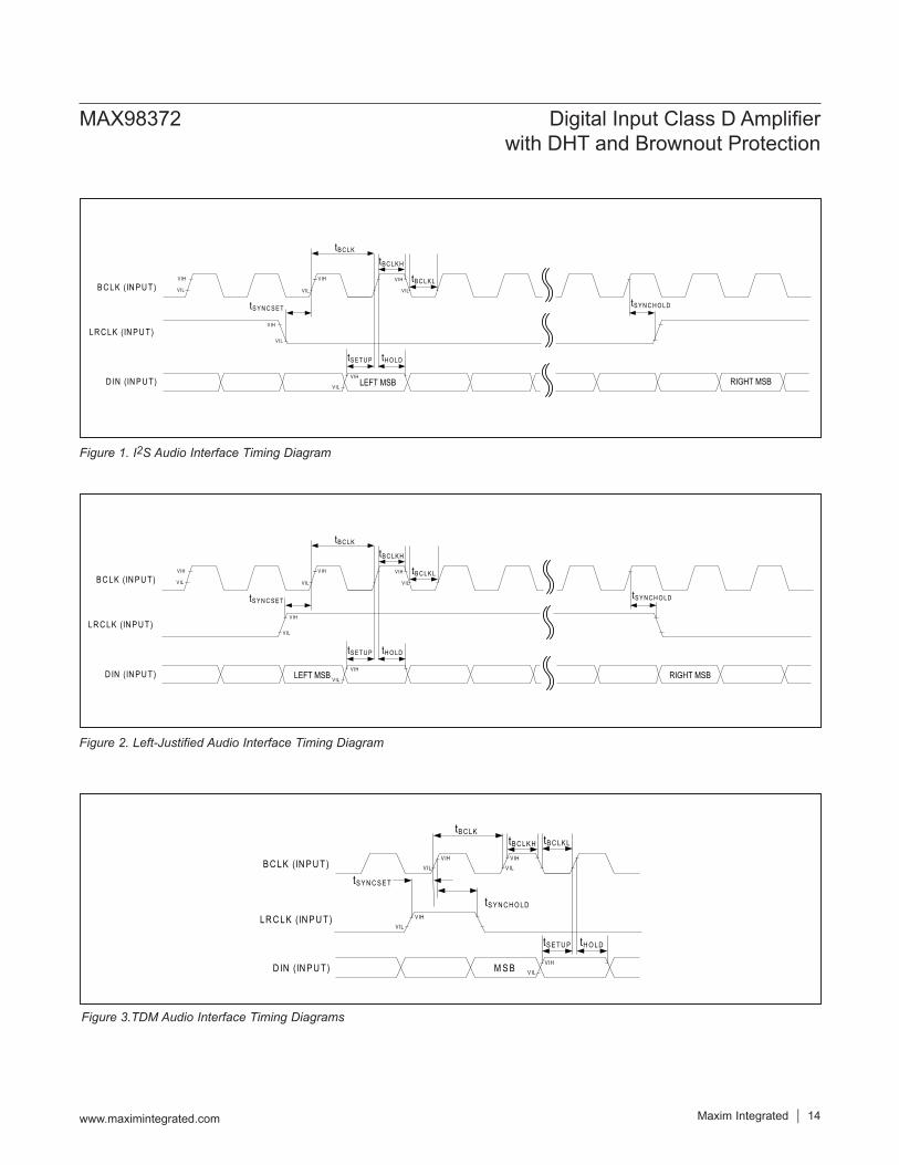
Figure 1. I2S Audio Interface Timing Diagram
LR C LK (IN P U T)
B C LK (IN P U T)
D IN (IN P U T) LEFT MSB
tH O LDtS E TU P
tB C LK H
tB C LK L
tB C LK
tS Y N C S E T
RIGHT MSB
tS Y N C H O LD
V IH
V IL
V IH
V IL
V IH
V IH
V IL V IL
V IH
V IL
Figure 3.TDM Audio Interface Timing Diagrams
LR C LK (IN P U T)
B C LK (IN P U T)
D IN (IN P U T)
tH O LDtS E TU P
tS Y N C H O LD
M S B
tB C LK H tB C LK LtB C LK
tS Y N C S E T
V ILV IH
V ILV IH
V ILV IH
V ILV IH
Figure 2. Left-Justified Audio Interface Timing Diagram
LR C LK (IN P U T)
B C LK (IN P U T)
D IN (IN P U T) LEFT MSB
tH O LDtS E TU P
tB C LK H
tB C LK L
tB C LK
tS Y N C S E T tS Y N C H O LD
V IH
V IL
V IH
V IL
V IH
V IH
V IL V IL
V IH
V IL RIGHT MSB
www.maximintegrated.com Maxim Integrated 14
MAX98372 Digital Input Class D Amplifier with DHT and Brownout Protection

Note 2: 100% production tested at TA = +25°C. Specifications over temperature limits are guaranteed by design.Note 3: Minimums and/or maximum limits shown are design targets and not 100% production tested.Note 4: CB in pF.Note 5: Digital filter performance is invariant over temperature and production tested at TA = +25°C.
I2C Timing Characteristics(VPVDD = 12V, VDVDD = VRESET = 1.8V, VGND = 0V, CPVDD = 1x 220µF, 2x 10µF, 2x 0.1µF, CVREFC = 1µF, CDVDD = 1µF, ZSPK = open, AC measurement bandwidth 20Hz to 22kHz, fS = 48kHz, 24-bit data, TA = TMIN to TMAX, unless, otherwise noted. Typical values are at TA = +25°C.) (Note 2)
PARAMETER SYMBOL CONDITIONS MIN TYP MAX UNITSI2C TIMING CHARACTERISTICS
Serial Clock Frequency fSCL 0 400 kHz
Bus Free Time Between STOP and START Conditions tBUF 1.3 µs
Hold Time (Repeated) START Condition tHD,STA 0.6 µs
SCL Pulse-Width Low tLOW 1.3 µsSCL Pulse-Width High tHIGH 0.6 µs
Setup Time for a Repeated START Condition tSU,STA 0.6 µs
Data Hold Time tHD,DAT 0 900 nsData Setup Time tSU,DAT 100 ns
SDA and SCL Receiving Rise Time (Note 4) tR
20 + 0.1CB
300 ns
SDA and SCL Receiving Fall Time (Note 4) tF
20 + 0.1CB
300 ns
SDA Transmitting Fall Time tF 20 250 ns
Setup Time for STOP Condition tSU,STO 0.6 µs
Bus Capacitance CB 400 pF
Pulse Width of Suppressed Spike tSP 0 50 ns
www.maximintegrated.com Maxim Integrated 15
MAX98372 Digital Input Class D Amplifier with DHT and Brownout Protection
(VPVDD = 12V, VDVDD = 1.8V, VGND = 0V, SPK_GAIN_MAX = 0x0B (20.5dB), fBCLK = 3.072MHz, fLRCLK = 48kHz, speaker loads (ZSPK) connected between OUTP and OUTN, TA = TMIN to TMAX, unless otherwise noted. Typical values are at TA = +25ºC.)
0.0
0.5
1.0
1.5
2.0
2.5
3.0
3.5
4.0
1.0 1.5 2.0
DVDD
SW
SHU
TDOW
N CU
RREN
T (µ
A)
DVDD VOLTAGE (V)
DVDD SOFTWARE SHUTDOWN CURRENTvs. DVDD VOLTAGE
ZSPK = ∞DAI PINS = GND
toc03
0.0
0.5
1.0
1.5
2.0
2.5
3.0
1.0 1.5 2.0
DVDD
QUI
ESCE
NT C
URRE
NT (m
A)
DVDD VOLTAGE (V)
DVDD QUIESCENT CURRENTvs. DVDD VOLTAGE
ZSPK = ∞
toc01
0
1
2
3
4
5
6
7
8
9
10
5 10 15
PVDD
QUI
ESCE
NT C
URRE
NT (m
A)
PVDD VOLTAGE (V)
PVDD QUIESCENT CURRENTvs. PVDD VOLTAGE
ZSPK = ∞
fSPK_SW = 472kHz
fSPK_SW = 330kHz
toc02
0.0
0.1
0.2
0.3
0.4
0.5
0.6
0.7
0.8
0.9
1.0
5 10 15
PVDD
SW
SHU
TDOW
N CU
RREN
T (µ
A)
PVDD VOLTAGE (V)
PVDD SOFTWARE SHUTDOWN CURRENTvs. PVDD VOLTAGE
ZSPK = ∞
toc04
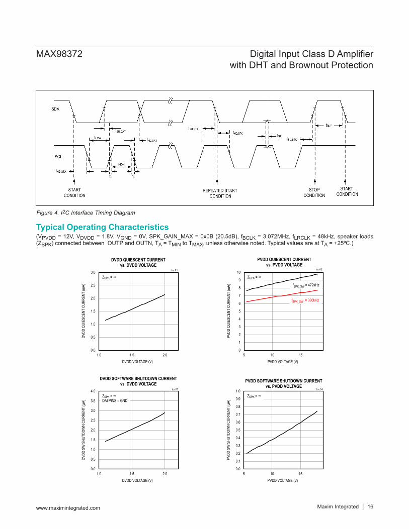
Figure 4. I2C Interface Timing Diagram
www.maximintegrated.com Maxim Integrated 16
MAX98372 Digital Input Class D Amplifier with DHT and Brownout Protection
Typical Operating Characteristics

(VPVDD = 12V, VDVDD = 1.8V, VGND = 0V, SPK_GAIN_MAX = 0x0B (20.5dB), fBCLK = 3.072MHz, fLRCLK = 48kHz, speaker loads (ZSPK) connected between OUTP and OUTN, TA = TMIN to TMAX, unless otherwise noted. Typical values are at TA = +25ºC.)
-100
-90
-80
-70
-60
-50
-40
-30
-20
-10
0
0.0001 0.001 0.01 0.1 1 10
THD+
N RA
TIO
(dB)
OUTPUT POWER (W)
THD+N RATIO vs.OUTPUT POWER
ZSPK = 8Ω + 68µHVPVDD = 12V
100Hz1kHz
6kHz
toc08
0
0.1
0.2
0.3
0.4
0.5
0.6
0.7
0.8
1.0 1.5 2.0
DVDD
HW
SHU
TDOW
N CU
RREN
T (µ
A)
DVDD VOLTAGE (V)
DVDD HARDWARE SHUTDOWN CURRENTvs. DVDD VOLTAGE
ZSPK = ∞VRST = 0V
toc05
-100
-90
-80
-70
-60
-50
-40
-30
-20
-10
0
0.0001 0.001 0.01 0.1 1 10 100
THD+
N RA
TIO
(dB)
OUTPUT POWER (W)
THD+N RATIO vs.OUTPUT POWER
ZSPK = 4Ω + 33µHVPVDD = 12V
100Hz
1kHz
6kHz
toc11
0.0
0.1
0.2
0.3
0.4
0.5
0.6
0.7
0.8
0.9
1.0
5 10 15
PVDD
HW
SHU
TDOW
N CU
RREN
T (µ
A)
PVDD VOLTAGE (V)
PVDD HARDWARE SHUTDOWN CURRENTvs. PVDD VOLTAGE
ZSPK = ∞VRST = 0V
toc06
-100
-90
-80
-70
-60
-50
-40
-30
-20
-10
0
10 100 1000 10000 100000
THD+
N RA
TIO
(dB)
FREQUENCY (Hz)
TOTAL HARMONIC DISTORTION PLUS NOISEvs. FREQUENCY
VPVDD = 5.5VZSPK = 8Ω + 68µH
POUT = 0.1W
POUT = 1W
toc12
-100
-90
-80
-70
-60
-50
-40
-30
-20
-10
0
0.0001 0.001 0.01 0.1 1 10
THD+
N RA
TIO
(dB)
OUTPUT POWER (W)
THD+N RATIOvs. OUTPUT POWER
ZSPK = 8Ω + 68µHVPVDD = 5.5V
100Hz1kHz
6kHz
toc07
-100
-90
-80
-70
-60
-50
-40
-30
-20
-10
0
10 100 1000 10000 100000
THD+
N RA
TIO
(dB)
FREQUENCY (Hz)
TOTAL HARMONIC DISTORTION PLUS NOISEvs. FREQUENCY
VPVDD = 12VZspk = 8Ω + 68µH
POUT = 1W
POUT = 4W
toc13
-100
-90
-80
-70
-60
-50
-40
-30
-20
-10
0
0.0001 0.001 0.01 0.1 1 10 100
THD+
N RA
TIO
(dB)
OUTPUT POWER (W)
THD+N RATIO vs.OUTPUT POWER
ZSPK = 8Ω + 68µHVPVDD = 17V
100Hz
1kHz
6kHz
toc09
-100
-90
-80
-70
-60
-50
-40
-30
-20
-10
0
0.0001 0.001 0.01 0.1 1 10
THD+
N RA
TIO
(dB)
OUTPUT POWER (W)
THD+N RATIO vs.OUTPUT POWER
ZSPK = 4Ω + 33µHVPVDD = 5.5V
100Hz
1kHz
6kHz
toc10
Maxim Integrated 17www.maximintegrated.com
MAX98372 Digital Input Class D Amplifier with DHT and Brownout Protection
Typical Operating Characteristics (continued)

(VPVDD = 12V, VDVDD = 1.8V, VGND = 0V, SPK_GAIN_MAX = 0x0B (20.5dB), fBCLK = 3.072MHz, fLRCLK = 48kHz, speaker loads (ZSPK) connected between OUTP and OUTN, TA = TMIN to TMAX, unless otherwise noted. Typical values are at TA = +25ºC.)
0.0
0.5
1.0
1.5
2.0
2.5
3.0
3.5
4.0
4.5
5.0
1 10 100
OUTP
UT P
OWER
(W)
LOAD RESISTANCE (Ω)
OUTPUT POWERvs. LOAD RESISTANCE
VPVDD = 5.5V
THD+N = 10%
THD+N = 1%
toc17
-100
-90
-80
-70
-60
-50
-40
-30
-20
-10
0
10 100 1000 10000 100000
THD+
N RA
TIO
(dB)
FREQUENCY (Hz)
TOTAL HARMONIC DISTORTION PLUS NOISEvs. FREQUENCY
VPVDD = 17VZSPK = 8Ω + 68µH
POUT = 1W
POUT = 4W
toc14
0
5
10
15
20
25
5 10 15 20
OUTP
UT P
OWER
(W)
PVDD SUPPLY VOLTAGE (V)
OUTPUT POWER vs.PVDD SUPPLY VOLTAGE
ZSPK = 8Ω + 68µH
1% THD+N
10% THD+N
toc20
-100
-90
-80
-70
-60
-50
-40
-30
-20
-10
0
10 100 1000 10000 100000
THD+
N RA
TIO
(dB)
FREQUENCY (Hz)
TOTAL HARMONIC DISTORTION PLUS NOISEvs. FREQUENCY
VPVDD = 5.5VZSPK = 4Ω + 33µH
POUT = 0.1W
POUT = 1W
toc15
0
2
4
6
8
10
12
14
16
18
20
5 7 9 11 13
OUTP
UT P
OWER
(W)
PVDD SUPPLY VOLTAGE (V)
OUTPUT POWER vs.PVDD SUPPLY VOLTAGE
ZSPK = 4Ω + 33µH
1% THD+N
10% THD+N
toc21
-100
-90
-80
-70
-60
-50
-40
-30
-20
-10
0
10 100 1000 10000 100000
THD+
N RA
TIO
(dB)
FREQUENCY (Hz)
TOTAL HARMONIC DISTORTION PLUS NOISEvs. FREQUENCY
VPVDD = 12VZSPK = 4Ω + 33µH
POUT = 1W
POUT = 8W
toc16
-0.5
-0.4
-0.3
-0.2
-0.1
0
0.1
0.2
0.3
0.4
0.5
20 200 2000 20000
NORM
ALIZ
ED G
AIN
(dB)
FREQUENCY (Hz)
NORMALIZED GAINvs. FREQUENCY
NORMALIZED TO 1kHzZSPK = 8Ω + 68µH
fS = 96kHz
fS = 48kHzfS = 44.1kHz
fS = 32kHz
toc22
0
2
4
6
8
10
12
14
16
18
20
1 10 100
OUTP
UT P
OWER
(W)
LOAD RESISTANCE (Ω)
OUTPUT POWERvs. LOAD RESISTANCE
VPVDD = 12V
THD+N = 10%
THD+N = 1%
toc18
0
5
10
15
20
25
1 10 100
OUTP
UT P
OWER
(W)
LOAD RESISTANCE (Ω)
OUTPUT POWERvs. LOAD RESISTANCE
VPVDD = 17V
THD+N = 10%
THD+N = 1%
toc19
Maxim Integrated 18www.maximintegrated.com
MAX98372 Digital Input Class D Amplifier with DHT and Brownout Protection
Typical Operating Characteristics (continued)

(VPVDD = 12V, VDVDD = 1.8V, VGND = 0V, SPK_GAIN_MAX = 0x0B (20.5dB), fBCLK = 3.072MHz, fLRCLK = 48kHz, speaker loads (ZSPK) connected between OUTP and OUTN, TA = TMIN to TMAX, unless otherwise noted. Typical values are at TA = +25ºC.)
0
10
20
30
40
50
60
70
80
90
100
0 5 10 15 20
EFFI
CIEN
CY (%
)
OUTPUT POWER (W)
EFFICIENCY vs.OUTPUT POWER
VPVDD = 17VZSPK = 8Ω + 68μH
fSPK = 472kHz
fSPK = 330kHz
toc26
0
10
20
30
40
50
60
70
80
90
0 5 10 15 20
EFFI
CIEN
CY (%
)
OUTPUT POWER (W)
EFFICIENCY vs.OUTPUT POWER
VPVDD = 12VZSPK = 4Ω + 33μH
fSPK = 472kHz
fSPK = 330kHz
toc23
0
10
20
30
40
50
60
70
80
90
100
0 2 4 6 8 10 12
EFFI
CIEN
CY (%
)
OUTPUT POWER (W)
EFFICIENCY vs.OUTPUT POWER
VPVDD = 12VZSPK = 8Ω + 68μH
fSPK = 472kHz
fSPK = 330kHz
toc29
0
10
20
30
40
50
60
70
80
90
0.001 0.01 0.1 1 10 100
EFFI
CIEN
CY (%
)
OUTPUT POWER (W)
EFFICIENCY vs.OUTPUT POWER
VPVDD = 12VZSPK = 4Ω + 33μH
fSPK = 472kHz
fSPK = 330kHz
toc24
0
10
20
30
40
50
60
70
80
90
100
0.001 0.01 0.1 1 10 100
EFFI
CIEN
CY (%
)
OUTPUT POWER (W)
EFFICIENCY vs.OUTPUT POWER
VPVDD = 12VZSPK = 8Ω + 68μH
fSPK = 472k
fSPK = 330kHz
toc30
0.0
0.5
1.0
1.5
2.0
2.5
3.0
3.5
4.0
0.001 0.01 0.1 1 10 100
POW
ER D
ISSI
PATI
ON (W
)
OUTPUT POWER (W)
POWER DISSIPATIONvs. OUTPUT POWER
VPVDD = 12VZSPK = 4Ω + 33μH
fSPK = 472kHz
fSPK = 330kHz
toc25
0.0
0.2
0.4
0.6
0.8
1.0
1.2
0.001 0.01 0.1 1 10 100
POW
ER D
ISSI
PATI
ON (W
)
OUTPUT POWER (W)
POWER DISSIPATIONvs. OUTPUT POWER
VPVDD = 12VZSPK = 8Ω + 68μH
fSPK = 472kHz
fSPK = 330kHz
toc31
0
10
20
30
40
50
60
70
80
90
100
0.001 0.01 0.1 1 10 100
EFFI
CIEN
CY (%
)
OUTPUT POWER (W)
EFFICIENCY vs.OUTPUT POWER
VPVDD = 17VZSPK = 8Ω + 68μH
fSPK = 472kHz
fSPK = 330kHz
toc27
0.0
0.5
1.0
1.5
2.0
2.5
0.001 0.01 0.1 1 10 100
POW
ER D
ISSI
PATI
ON (W
)
OUTPUT POWER (W)
POWER DISSIPATIONvs. OUTPUT POWER
VPVDD = 17VZSPK = 8Ω + 68μH
fSPK = 472kHz
fSPK = 330kHz
toc28
Maxim Integrated 19www.maximintegrated.com
MAX98372 Digital Input Class D Amplifier with DHT and Brownout Protection
Typical Operating Characteristics (continued)

(VPVDD = 12V, VDVDD = 1.8V, VGND = 0V, SPK_GAIN_MAX = 0x0B (20.5dB), fBCLK = 3.072MHz, fLRCLK = 48kHz, speaker loads (ZSPK) connected between OUTP and OUTN, TA = TMIN to TMAX, unless otherwise noted. Typical values are at TA = +25ºC.)
0
20
40
60
80
100
120
140
1.1 1.3 1.5 1.7 1.9
PSRR
(dB)
DVDD SUPPLY VOLTAGE (V)
POWER-SUPPLY REJECTION RATIOvs. DVDD SUPPLY VOLTAGE
VRIPPLE = 100mVP-Pfs=1kHz
toc35
0
10
20
30
40
50
60
70
80
90
100
10 100 1000 10000 100000
PSRR
(dB)
FREQUENCY (Hz)
PVDD POWER-SUPPLY REJECTION RATIOvs. FREQUENCY
VRIPPLE = 100mVP-PZSPK = ∞
toc32
SCL1V/div
SPKOUT5V/div
toc38
4ms/div
VOUTN
VINSIDE
VBACKUP
SOFTWARE DISABLETURN-OFF RESPONSE
VOLUME RAMPING ENABLED
0
10
20
30
40
50
60
70
80
90
100
5 10 15 20
PSRR
(dB)
PVDD SUPPLY VOLTAGE (V)
POWER-SUPPLY REJECTION RATIO vs.PVDD SUPPLY VOLTAGE
VRIPPLE = 100mVP-Pfs = 1kHz
toc33
SCL1V/div
SPKOUT5V/div
toc39
2ms/div
VOUTN
VINSIDE
VBACKUP
SOFTWARE DISABLETURN-OFF RESPONSE
VOLUME RAMPING DISABLED
0
20
40
60
80
100
120
140
10 100 1000 10000 100000
PSRR
(dB)
FREQUENCY (Hz)
DVDD POWER-SUPPLY REJECTION RATIOvs. FREQUENCY
VRIPPLE = 100mVP-P
toc34
RST1V/div
SPKOUT5V/div
toc40
800µs/div
VOUTN
VINSIDE
VBACKUP
HARDWARE RESETTURN-OFF RESPONSE
SCL1V/div
SPKOUT5V/div
toc36
4ms/div
VOUTN
VINSIDE
VBACKUP
SOFTWARE ENABLETURN-ON RESPONSE
VOLUME RAMPING ENABLED
SCL1V/div
SPKOUT5V/div
toc37
2ms/div
VOUTN
VINSIDE
VBACKUP
SOFTWARE ENABLETURN-ON RESPONSE
VOLUME RAMPING DISABLED
Maxim Integrated 20www.maximintegrated.com
MAX98372 Digital Input Class D Amplifier with DHT and Brownout Protection
Typical Operating Characteristics (continued)

(VPVDD = 12V, VDVDD = 1.8V, VGND = 0V, SPK_GAIN_MAX = 0x0B (20.5dB), fBCLK = 3.072MHz, fLRCLK = 48kHz, speaker loads (ZSPK) connected between OUTP and OUTN, TA = TMIN to TMAX, unless otherwise noted. Typical values are at TA = +25ºC.)
-140
-120
-100
-80
-60
-40
-20
0
20
40
0 5000 10000 15000 20000
AMPL
ITUD
E (d
BV)
FREQUENCY (Hz)
INBAND OUTPUT SPECTRUM
ZSPK = 8Ω + 68µHfS = 32kHz
toc44
BCLK2V/div
LRCLK1V/div
SPKOUT5V/div
toc41
2ms
VOUTN
VINSIDE
VBACKUP
BCLK REMOVALTURN-OFF RESPONSE
-140
-120
-100
-80
-60
-40
-20
0
20
40
0 5000 10000 15000 20000
AMPL
ITUD
E (d
BV)
FREQUENCY (Hz)
INBAND OUTPUT SPECTRUMZSPK = 8Ω + 68µH
fS = 44.1kHz
toc47
-140
-120
-100
-80
-60
-40
-20
0
20
40
0 5000 10000 15000 20000
AMPL
ITUD
E (d
BV)
FREQUENCY (Hz)
INBAND OUTPUT SPECTRUMZSPK = 8Ω + 68µH
fS = 32kHz
toc42
-140
-120
-100
-80
-60
-40
-20
0
20
40
0 5000 10000 15000 20000
AMPL
ITUD
E (d
BV)
FREQUENCY (Hz)
INBAND OUTPUT SPECTRUMZSPK = 8Ω + 68µH
fS = 48kHz
toc48
-140
-120
-100
-80
-60
-40
-20
0
20
40
0 5000 10000 15000 20000
AMPL
ITUD
E (d
BV)
FREQUENCY (Hz)
INBAND OUTPUT SPECTRUMZSPK = 8Ω + 68µH
fS = 32kHz
toc43
-140
-120
-100
-80
-60
-40
-20
0
20
40
0 5000 10000 15000 20000
AMPL
ITUD
E (d
BV)
FREQUENCY (Hz)
INBAND OUTPUT SPECTRUMZSPK = 8Ω + 68µH
fS = 48kHz
toc49
-140
-120
-100
-80
-60
-40
-20
0
20
40
0 5000 10000 15000 20000
AMPL
ITUD
E (d
BV)
FREQUENCY (Hz)
INBAND OUTPUT SPECTRUMZSPK = 8Ω + 68µH
fS = 44.1kHz
toc45
-140
-120
-100
-80
-60
-40
-20
0
20
40
0 5000 10000 15000 20000
AMPL
ITUD
E (d
BV)
FREQUENCY (Hz)
INBAND OUTPUT SPECTRUMZSPK = 8Ω + 68µH
fS = 44.1kHz
toc46
Maxim Integrated 21www.maximintegrated.com
MAX98372 Digital Input Class D Amplifier with DHT and Brownout Protection
Typical Operating Characteristics (continued)
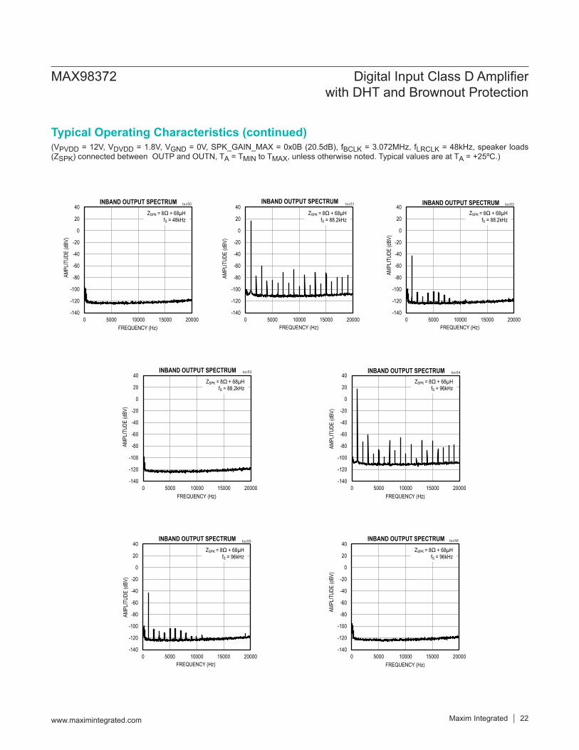
(VPVDD = 12V, VDVDD = 1.8V, VGND = 0V, SPK_GAIN_MAX = 0x0B (20.5dB), fBCLK = 3.072MHz, fLRCLK = 48kHz, speaker loads (ZSPK) connected between OUTP and OUTN, TA = TMIN to TMAX, unless otherwise noted. Typical values are at TA = +25ºC.)
-140
-120
-100
-80
-60
-40
-20
0
20
40
0 5000 10000 15000 20000
AMPL
ITUD
E (d
BV)
FREQUENCY (Hz)
INBAND OUTPUT SPECTRUMZSPK = 8Ω + 68µH
fS = 88.2kHz
toc53
-140
-120
-100
-80
-60
-40
-20
0
20
40
0 5000 10000 15000 20000
AMPL
ITUD
E (d
BV)
FREQUENCY (Hz)
INBAND OUTPUT SPECTRUMZSPK = 8Ω + 68µH
fS = 48kHz
toc50
-140
-120
-100
-80
-60
-40
-20
0
20
40
0 5000 10000 15000 20000
AMPL
ITUD
E (d
BV)
FREQUENCY (Hz)
INBAND OUTPUT SPECTRUMZSPK = 8Ω + 68µH
fS = 96kHz
toc56
-140
-120
-100
-80
-60
-40
-20
0
20
40
0 5000 10000 15000 20000
AMPL
ITUD
E (d
BV)
FREQUENCY (Hz)
INBAND OUTPUT SPECTRUMZSPK = 8Ω + 68µH
fS = 88.2kHz
toc51
-140
-120
-100
-80
-60
-40
-20
0
20
40
0 5000 10000 15000 20000
AMPL
ITUD
E (d
BV)
FREQUENCY (Hz)
INBAND OUTPUT SPECTRUMZSPK = 8Ω + 68µH
fS = 88.2kHz
toc52
-140
-120
-100
-80
-60
-40
-20
0
20
40
0 5000 10000 15000 20000
AMPL
ITUD
E (d
BV)
FREQUENCY (Hz)
INBAND OUTPUT SPECTRUMZSPK = 8Ω + 68µH
fS = 96kHz
toc54
-140
-120
-100
-80
-60
-40
-20
0
20
40
0 5000 10000 15000 20000
AMPL
ITUD
E (d
BV)
FREQUENCY (Hz)
INBAND OUTPUT SPECTRUMZSPK = 8Ω + 68µH
fS = 96kHz
toc55
Maxim Integrated 22www.maximintegrated.com
MAX98372 Digital Input Class D Amplifier with DHT and Brownout Protection
Typical Operating Characteristics (continued)

1
A
B
C
D
E
2 3 4 5 6
OUTNSNS PVDD PVDD DVDD ADDR1 SCL
OUTN OUTN PGND DGND ADDR0 SDA
PGND PGND PGND AGND DOUT LRCLK
OUTP OUTP PGND AGND IRQ DIN
OUTPSNS PVDD PVDD VREFC RESET BCLK
DIGITAL ANALOG HIGH POWER
TOP VIEW (BUMP SIDE DOWN)
WLP(2.2mm x 2.7mm)
www.maximintegrated.com Maxim Integrated 23
MAX98372 Digital Input Class D Amplifier with DHT and Brownout Protection
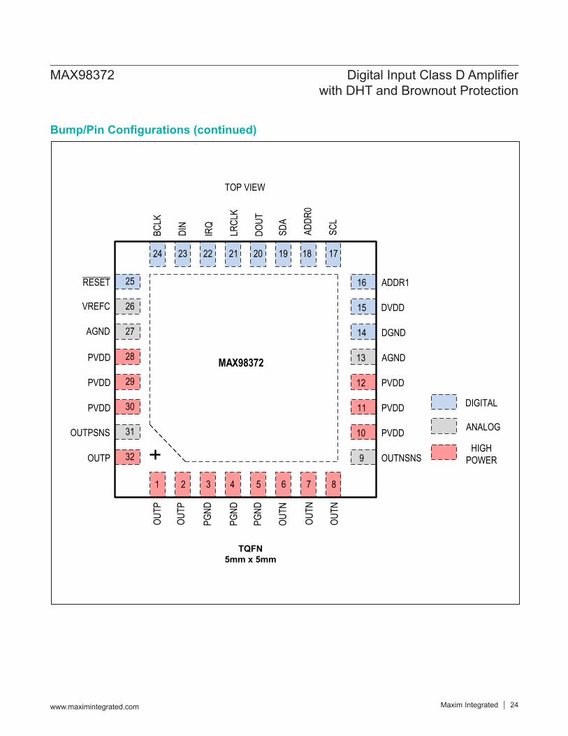
Bump/Pin Configurations
1 2 3 4 5 6 7 8
10
9
11
12
13
14
15
16
1718192021222324
25
26
27
28
29
30
31
32
OUTP
OUTP
OUTP
PGND
PGND
PGND
OUTN
OUTN
OUTN
OUTNSNS
PVDD
PVDD
PVDD
AGND
DGND
DVDD
ADDR1
SCL
ADDR
0
SDA
DOUT
LRCL
K
IRQ
DIN
BCLK
RESET
VREFC
AGND
PVDD
PVDD
PVDD
OUTPSNS
MAX98372
DIGITAL
HIGH POWER
ANALOG
TOP VIEW
TQFN5mm x 5mm
Bump/Pin Configurations (continued)
www.maximintegrated.com Maxim Integrated 24
MAX98372 Digital Input Class D Amplifier with DHT and Brownout Protection

PINNAME SUPPLY
RAIL FUNCTIONWLP TQFNA1 9 OUTNSNS PVDD Negative Speaker Amplifier Output Sense. If not used, connect to OUTN.
A2, A3 E2, E3
10-12, 28-30 PVDD — Speaker Amplifier Power Supply. Bypass each bump pair to PGND with a 10µF
and a 0.1µF, and a single 220µF per device.
A4 15 DVDD — Digital Core, Digital Audio Interface, and I2C Control Power Supply. Bypass to DGND with a 1µF.
A5 16 ADDR1 DVDD Four-Level I2C Slave Address Select Input. See the Slave Address Selection sec-tion for additional information (Table 40).
A6 17 SCL DVDD I2C Control Clock Input B1, B2 6-8 OUTN PVDD Negative Speaker Amplifier Output
B3, C1–C3, D3 3-5 PGND — Speaker Amplifier Ground
B4 14 DGND — Digital Ground
B5 18 ADDR0 DVDD Four-Level I2C Slave Address Select Input. See the Slave Address Selection sec-tion for additional information (Table 40).
B6 19 SDA DVDD I2C Control Data Input/Output C4, D4 27, 13 AGND — Analog Ground
C5 20 DOUT DVDD Bidirectional ICC Link Data
C6 21 LRCLK DVDDDAI Left/Right Clock Input. LRCLK is the audio sample rate clock and determines whether audio data is routed to the left or right channel. In TDM mode, LRCLK is a frame sync pulse with programmable width.
D1, D2 1-2, 32 OUTP PVDD Positive Speaker Amplifier Output
D5 22 IRQ DVDDHardware Interrupt Output. IRQ can be programmed to pull low when individual bits in the flag registers change value. Connect a 10kΩ pullup resistor for full output swing.
D6 23 DIN DVDD DAI Audio Data InputE1 31 OUTPSNS PVDD Positive Speaker Amplifier Output Sense. If not used, connect to OUTP.E4 26 VREFC PVDD Internal Regulator Decoupling Point. Bypass to AGND with a 1µF.
E5 25 RESET DVDD Active-Low Hardware Reset. Drive low to place the device into low power reset mode and reset the device registers to their power-on-reset (POR) states.
E6 24 BCLK DVDD DAI Bit Clock Input
www.maximintegrated.com Maxim Integrated 25
MAX98372 Digital Input Class D Amplifier with DHT and Brownout Protection
Bump/Pin Description

Detailed DescriptionThe MAX98372 is a high-efficiency mono Class D audio amplifier that features thermal foldback protection and ADCs for sensing battery supply voltage and onboard temperature.The MAX98372 can operate over a wide range of supply voltage (PVDD), and has extensive on-board digital signal processing to enable dynamic headroom tracking (DHT). This feature automatically adjusts the output signal to fit into the available supply voltage range. The DHT can be completely bypassed for operation with fixed, regulated supply voltages.The MAX98372 provides automatic level control (ALC) for battery brownout protection. This is achieved by reducing amplifier gain when the battery voltage drops below the selected threshold. ALC threshold, maximum attenuation, and attack/release rates are programmable.Active emissions limiting edge rate and overshoot control circuitry, together with Class D modulation, minimize the electromagnetic interference (EMI) traditionally associated with Class D amplifiers. In systems that use less than 18in of speaker cable, an output filter is unnecessary to meet standard EMI limits.Two ADCs monitor PVDD supply voltage and die temperature. The PVDD supply voltage value can be read using the I2C interface. The temperature ADC can
be read back through I2C, however, accurate readings only occur after the die temperature exceeds +100°C.The DAI supports I2S, left-justified, and TDM formatted data at the following sample rates: 32kHz, 44.1kHz, 48kHz, 88.2kHz, and 96kHz. Audio bit depths of 16, 24, and 32 bits are supported for input data. The DAI operates from BCLK to allow the device to function without MCLK.Thermal foldback allows the device to smoothly attenuate the audio output in an effort to prevent destructive thermal behavior. Above a set threshold, the gain of the replay path reduces at a (user programmable) dB/°C rate to a 12dB maximum attenuation. Thermal monitoring capabilities alert the host when die temperature has triggered the thermal foldback circuit, or is approaching the maximum operating temperature. If maximum die temperature is exceeded, the device shuts down to protect itself. Short- circuit protection ensures that accidental shorts or high- current events do not cause damage to the IC.Device status is communicated to the host through a hardware interrupt (IRQ) and status registers accessible through the I2C interface.The MAX98372 is fully programmable through the I2C interface. ADDR0, ADDR1 connections select one of sixteen I2C slave addresses. Shutdown mode is directly controlled through the I2C interface, or a hardware shutdown can be asserted through the RESET pin.
Table 1. MAX98372 Control Register MapREGISTER DESCRIPTION REGISTER CONTENTS POR
STATEADDR NAME R/W BIT 7 BIT 6 BIT 5 BIT 4 BIT 3 BIT2 BIT1 BIT 0 INTERRUPTS
0x01INTERRUPT STATUS 0
R — —THRMFB_ STATUS
—THRM WRN_
STATUS—
THRM SHDN_ STATUS
— 0x00
0x02INTERRUPT STATUS 1
R —ICCOVC_ STATUS
LMTRACT_ STATUS
INVAL SLOT_
STATUS
DHTACT_ STATUS
SPK CURNT_ STATUS
PVDD OVFL_
STATUS
PVDD UVLO_ STATUS
0x01
0x03INTERRUPT
STATE 0R — —
THRMFB_ END_ STATE
THRMFB_ BGN_ STATE
THRM WRN_END
_STATE
THRM WRN_BGN
_STATE
THRM SHDN_END
_STATE
THRM SHDN_BGN
_STATE0x00
0x04INTERRUPT
STATE 1R —
ICCOVC_ STATE
LMTRACT_ STATE
INVAL SLOT_ STATE
DHTACT_ STATE
SPK CURNT_ STATE
PVDD OVFL_ STATE
PVDD UVLO_ STATE
0x00
0x05INTERRUPT
FLAG 0R/W — —
THRMFB_ END_ FLAG
THRMFB_ BGN_ FLAG
THRM WRN_END_
FLAG
THRMWRN_BGN
_FLAG
THRM SHDN_
END_ FLAG
THRM SHDN_
BGN_ FLAG0x00
www.maximintegrated.com Maxim Integrated 26
MAX98372 Digital Input Class D Amplifier with DHT and Brownout Protection
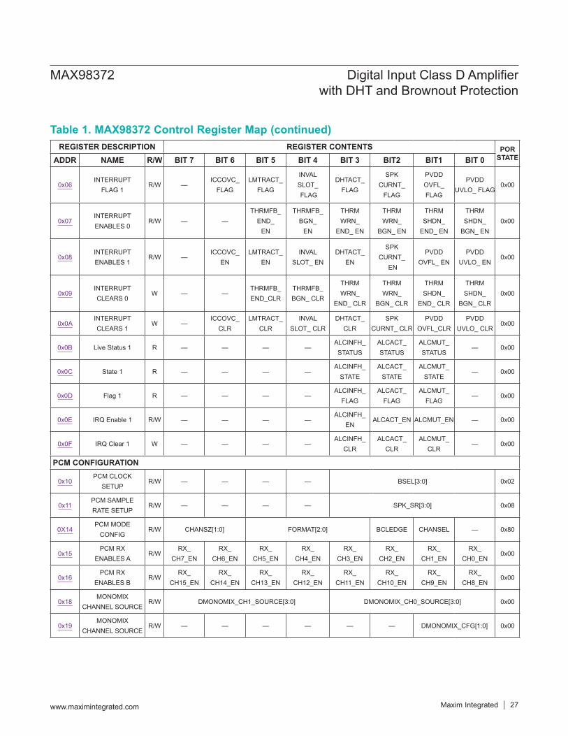
Table 1. MAX98372 Control Register Map (continued)REGISTER DESCRIPTION REGISTER CONTENTS POR
STATEADDR NAME R/W BIT 7 BIT 6 BIT 5 BIT 4 BIT 3 BIT2 BIT1 BIT 0
0x06INTERRUPT
FLAG 1R/W —
ICCOVC_ FLAG
LMTRACT_ FLAG
INVAL SLOT_ FLAG
DHTACT_ FLAG
SPK CURNT_
FLAG
PVDD OVFL_ FLAG
PVDD UVLO_ FLAG
0x00
0x07INTERRUPT ENABLES 0
R/W — —THRMFB_
END_ EN
THRMFB_ BGN_
EN
THRM WRN_
END_ EN
THRM WRN_
BGN_ EN
THRM SHDN_
END_ EN
THRM SHDN_
BGN_ EN0x00
0x08INTERRUPT ENABLES 1
R/W —ICCOVC_
ENLMTRACT_
ENINVAL
SLOT_ ENDHTACT_
EN
SPK CURNT_
EN
PVDD OVFL_ EN
PVDD UVLO_ EN
0x00
0x09INTERRUPT CLEARS 0
W — —THRMFB_ END_CLR
THRMFB_ BGN_ CLR
THRM WRN_
END_ CLR
THRM WRN_
BGN_ CLR
THRM SHDN_
END_ CLR
THRM SHDN_
BGN_ CLR0x00
0x0AINTERRUPT CLEARS 1
W —ICCOVC_
CLRLMTRACT_
CLRINVAL
SLOT_ CLRDHTACT_
CLRSPK
CURNT_ CLRPVDD
OVFL_CLRPVDD
UVLO_ CLR0x00
0x0B Live Status 1 R — — — —ALCINFH_ STATUS
ALCACT_ STATUS
ALCMUT_ STATUS
— 0x00
0x0C State 1 R — — — —ALCINFH_
STATEALCACT_
STATEALCMUT_
STATE— 0x00
0x0D Flag 1 R — — — —ALCINFH_
FLAGALCACT_
FLAGALCMUT_
FLAG— 0x00
0x0E IRQ Enable 1 R/W — — — —ALCINFH_
ENALCACT_EN ALCMUT_EN — 0x00
0x0F IRQ Clear 1 W — — — —ALCINFH_
CLRALCACT_
CLRALCMUT_
CLR— 0x00
PCM CONFIGURATION
0x10PCM CLOCK
SETUPR/W — — — — BSEL[3:0] 0x02
0x11PCM SAMPLE RATE SETUP
R/W — — — — SPK_SR[3:0] 0x08
0X14PCM MODE
CONFIGR/W CHANSZ[1:0] FORMAT[2:0] BCLEDGE CHANSEL — 0x80
0x15PCM RX
ENABLES AR/W
RX_ CH7_EN
RX_ CH6_EN
RX_ CH5_EN
RX_ CH4_EN
RX_ CH3_EN
RX_ CH2_EN
RX_ CH1_EN
RX_ CH0_EN
0x00
0x16PCM RX
ENABLES BR/W
RX_ CH15_EN
RX_ CH14_EN
RX_ CH13_EN
RX_ CH12_EN
RX_ CH11_EN
RX_ CH10_EN
RX_ CH9_EN
RX_ CH8_EN
0x00
0x18MONOMIX
CHANNEL SOURCER/W DMONOMIX_CH1_SOURCE[3:0] DMONOMIX_CH0_SOURCE[3:0] 0x00
0x19MONOMIX
CHANNEL SOURCER/W — — — — — — DMONOMIX_CFG[1:0] 0x00
www.maximintegrated.com Maxim Integrated 27
MAX98372 Digital Input Class D Amplifier with DHT and Brownout Protection

Table 1. MAX98372 Control Register Map (continued)REGISTER DESCRIPTION REGISTER CONTENTS POR
STATEADDR NAME R/W BIT 7 BIT 6 BIT 5 BIT 4 BIT 3 BIT2 BIT1 BIT 0 DIGITAL FILTER PARAMETERS
0x1C DIGITAL FILTER R/WPVDD_FILT _TO_LMTR
PVDD_FILT _TO_DHT
PVDD_ADC_BW[1:0] — DACHPF[2:0] 0x00
0x1D
DAC BQ B0
R/W DAC_BQ_B0[23:16] 0x10
0x1E R/W DAC_BQ_B0[15:8] 0x00
0x1F R/W DAC_BQ_B0[7:0] 0x00
0x20
DAC BQ B1
R/W DAC_BQ_B1[23:16] 0x00
0x21 R/W DAC_BQ_B1[15:8] 0x00
0x22 R/W DAC_BQ_B1[7:0] 0x00
0x23
DAC BQ B2
R/W DAC_BQ_B2[23:16] 0x00
0x24 R/W DAC_BQ_B2[15:8] 0x00
0x25 R/W DAC_BQ_B2[7:0] 0x00
0x26
DAC BQ A0
R/W DAC_BQ_A0[23:16] 0x00
0x27 R/W DAC_BQ_A0[15:8] 0x00
0x28 R/W DAC_BQ_A0[7:0] 0x00
0x29
DAC BQ A1
R/W DAC_BQ_A1[23:16] 0x00
0x2A R/W DAC_BQ_A1[15:8] 0x00
0x2B R/W DAC_BQ_A1[7:0] 0x00
0x2DDIGITAL VOLUME
CONTROLR/W
DVOL_ RAMP_BYP
DVOL[6:0] 0x00
0x2E PATH GAIN R/W DPGA_CLIP[3:0] SPK_GAIN_MAX[3:0] 0x0B
DYNAMIC GAIN PARAMETERS
0x31DHT ROTATION
POINTR/W SPK_GAIN_MIN[3:0] DHT_VROT_PNT[3:0] 0x00
0x32 DHT ATTACK R/W — — — DHT_ATK_STEP[1:0] DHT_ATK_RATE[2:0] 0x18
0x33 DHT RELEASE R/W — — — DHT_REL_STEP[1:0] DHT_REL_RATE[2:0] 0x00
0x34PVDD ADC
MEASUREMENTR PVDD_ADC[7:0] 0x00
0x36THERMAL
FOLDBACKR/W THRM_HOLD[1:0] — — THRM_REL[1:0] THRM_SLOPE[1:0] 0xC0
0x37THERMAL ADC
MEASUREMENTR — — THRM_ADC_MEAS[5:0] 0x00
0x38THERMAL
FOLDBACK MIN TEMP
R/W — — THRM_MIN_TEMP[5:0] 0x00
0x39THERMAL
FOLDBACK LOW PASS FILTER
R/W — — — — — THRM_FILT_SEL[2:0] 0x03
www.maximintegrated.com Maxim Integrated 28
MAX98372 Digital Input Class D Amplifier with DHT and Brownout Protection

Table 1. MAX98372 Control Register Map (continued)REGISTER DESCRIPTION REGISTER CONTENTS POR
STATEADDR NAME R/W BIT 7 BIT 6 BIT 5 BIT 4 BIT 3 BIT2 BIT1 BIT 0
0x3APCM2 RXDHT ENABLES A
R/WRXDHT_ CH7_EN
RXDHT_ CH6_EN
RXDHT_ CH5_EN
RXDHT_ CH4_EN
RXDHT_ CH3_EN
RXDHT_ CH2_EN
RXDHT_ CH1_EN
RXDHT_ CH0_EN
0x00
0x3BPCM2 RXDHT ENABLES B
R/WRXDHT_ CH15_EN
RXDHT_ CH14_EN
RXDHT_ CH13_EN
RXDHT_ CH12_EN
RXDHT_ CH11_EN
RXDHT_ CH10_EN
RXDHT_ CH9_EN
RXDHT_ CH8_EN
0x00
0x3CPCM2 RXTHM
ENABLES AR/W
RXTHM_ CH7_EN
RXTHM_ CH6_EN
RXTHM_ CH5_EN
RXTHM_ CH4_EN
RXTHM_ CH3_EN
RXTHM_ CH2_EN
RXTHM_ CH1_EN
RXTHM_ CH0_EN
0x00
0x3DPCM2 RXTHM ENABLES B
R/WRXTHM_ CH15_EN
RXTHM_ CH14_EN
RXTHM_ CH13_EN
RXTHM_ CH12_EN
RXTHM_ CH11_EN
RXTHM_ CH10_EN
RXTHM_ CH9_EN
RXTHM_ CH8_EN
0x00
0x3EPCM2 TX \
ENABLES AR/W
TX_ CH7_EN
TX_ CH6_EN
TX_ CH5_EN
TX_ CH4_EN
TX_ CH3_EN
TX_ CH2_EN
TX_ CH1_EN
TX_ CH0_EN
0x00
0x3FPCM2 TX
ENABLES AR/W
TX_ CH15_EN
TX_ CH14_EN
TX_ CH13_EN
TX_ CH12_EN
TX_ CH11_EN
TX_ CH10_EN
TX_ CH9_EN
TX_ CH8_EN
0x00
0x40PCM2 DATA
ORDER SELECTR/W — — — —
DRIVE_ MODE
— — — 0x00
0x41PCM2 HiZ
MANUAL MODER/W — — — — — —
TX_ EXTRA_
HIZ— 0x00
0x42PCM2 TX HiZ ENABLES A
R/WTX_
CH7_HIZTX_
CH6_HIZTX_
CH5_HIZTX_
CH4_HIZTX_
CH3_HIZTX_
CH2_HIZTX_
CH1_HIZTX_
CH0_HIZ0x00
0x43PCM2 TX HiZ ENABLES B
R/WTX_
CH15_HIZTX_
CH14_HIZTX_
CH13_HIZTX_
CH12_HIZTX_
CH11_HIZTX_
CH10_HIZTX_
CH9_HIZTX_
CH8_HIZ0x00
ENABLES
0x49 SSM_CFG R/W — — — — — SSM_MODINDEX[2:0] 0x01
0x4ASPEAKER ENABLE
R/WSPK_
SWCLK— SPK_SSM[1:0] SPK_EDGE[1:0] — SPK_EN 0x00
0x4BDYNAMIC GAIN
ENABLESR/W — — — — — PVADC_EN LMTR_EN DHT_EN 0x00
0x4CTHERMAL
FOLDBACK ENABLER/W — — — — — — —
THERM_ FB_EN
0x00
0x4D RESTART BEHAVIOR R/W — — — —CMON_ AUTO_
RESTART
CMON_ ENA
OVC_ SEL
TSHDN_ AUTO_
RESTART0x00
0x4E ICC LINK ENABLE R/W — — — — —ALC_LINK_
ENTHM_
LINK_ENDHT_
LINK_EN0x00
0x50 GLOBAL ENABLE R/W — — — — — — — EN 0x00
0x51 SOFTWARE RESET W — — — — — — — RST 0x00
0x55LIMITER ATTACK AND RELEASE
R/W — — LMTR_REL_RATE[2:0] LMTR_ATK_RATE[2:0] 0x30
www.maximintegrated.com Maxim Integrated 29
MAX98372 Digital Input Class D Amplifier with DHT and Brownout Protection

Table 1. MAX98372 Control Register Map (continued)REGISTER DESCRIPTION REGISTER CONTENTS POR
STATEADDR NAME R/W BIT 7 BIT 6 BIT 5 BIT 4 BIT 3 BIT2 BIT1 BIT 0
0x57Digital Filter Dither
EnableR/W — — — — — —
AUTO_ DITHER_EN
DFILT_ DITH_EN
0x03
0x58LIMITER
THRESHOLD SELECT
R/W — — — — — — LMTR_TH_SEL[1:0] 0x00
0x59LIMITER MANUAL
THRESHOLDR/W — — — LMTR_THC[4:0] 0x00
0x5CICC PAD
CONTROLR/W —
ICC_OC_ ENA
ICC_ DOUTEN_
EXTFF
ICC_ DOUT_ EXTFF
ICC_PAD_CTRL[3:0] 0x00
0x60PCM2 RXALC
Enables AR/W
PCM2_RXAL_ CH7_EN
PCM2_RXAL_ CH6_EN
PCM2_RXAL_ CH5_EN
PCM2_RXALC_ CH4_EN
PCM2_RXALC_ CH3_EN
PCM2_RXAL_ CH2_EN
PCM2_RXAL_ CH1_EN
PCM2_RXAL_ CH0_EN
0x00
0x61PCM2 RXALC
Enables BR/W
PCM2_RXAL_ CH15_EN
PCM2_RXAL_ CH14_EN
PCM2_RXAL_ CH13_EN
PCM2_RXALC_ CH12_EN
PCM2_RXALC_ CH11_EN
PCM2_RXAL_ CH10_EN
PCM2_RXAL_ CH9_EN
PCM2_RXAL_ CH8_EN
0x00
0x62 THRESHOLD R/W — ALC_RANGE ALC_EN ALC_TH[4:0] 0x06
0x63 ALC ATTACK R/W ALC_ATK_STEP[3:0] — ALC_ATK_RATE[2:0] 0x00
0x64 ALC ATTEN and RLS R/W ALC_MAX_ATTEN[3:0] — ALC_RLS_RATE[2:0] 0x80
0x65ALC INFINITE HOLD
RELEASER/W ALC_RLS_CFG[1:0] — — — — —
ALC_RLS_ TGR
0x00
0x66ALC
CONFIGURATIONR/W
ALC_MUTE_EN
ALC_MUTE_DLY[2:0] — ALC_RLS_DBT[2:0] 0x92
0xFF REV ID R REVID[7:0] 0x41
www.maximintegrated.com Maxim Integrated 30
MAX98372 Digital Input Class D Amplifier with DHT and Brownout Protection
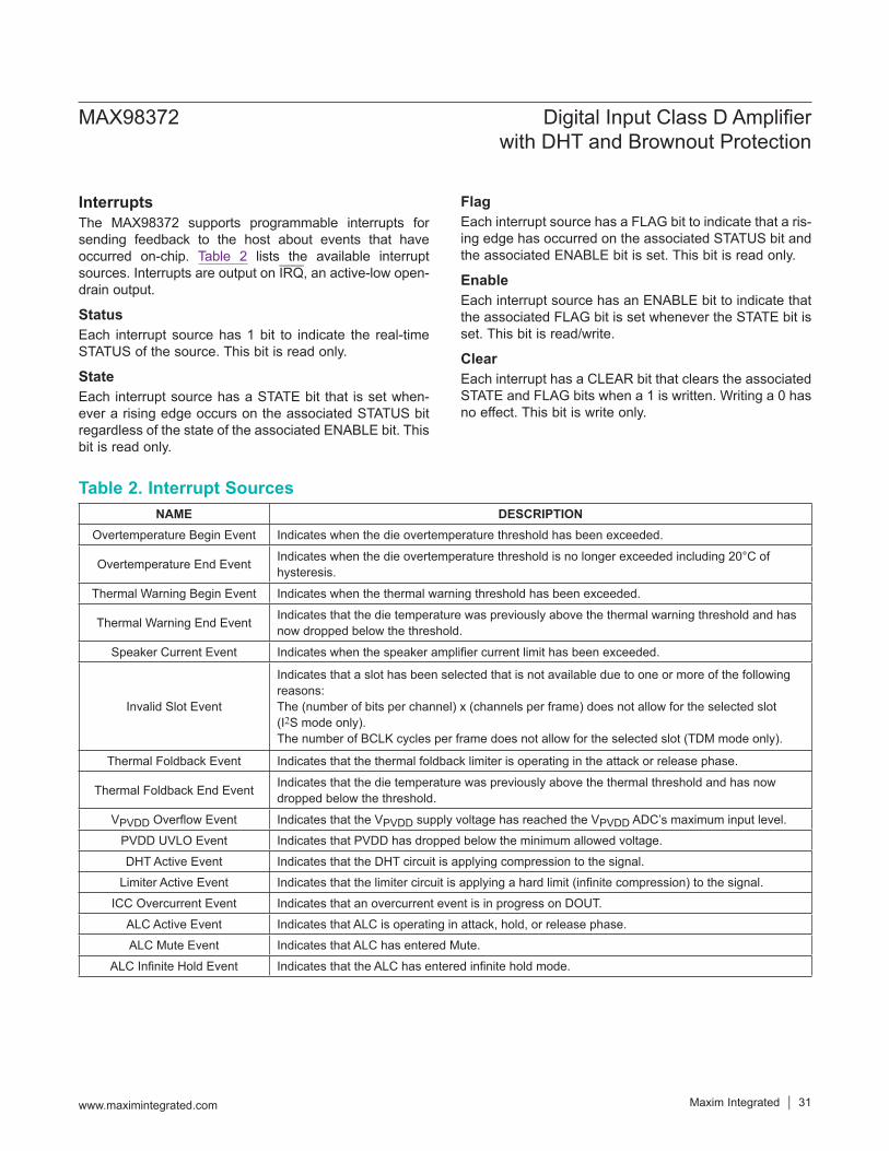
InterruptsThe MAX98372 supports programmable interrupts for sending feedback to the host about events that have occurred on-chip. Table 2 lists the available interrupt sources. Interrupts are output on IRQ, an active-low open-drain output.
StatusEach interrupt source has 1 bit to indicate the real-time STATUS of the source. This bit is read only.
StateEach interrupt source has a STATE bit that is set when-ever a rising edge occurs on the associated STATUS bit regardless of the state of the associated ENABLE bit. This bit is read only.
FlagEach interrupt source has a FLAG bit to indicate that a ris-ing edge has occurred on the associated STATUS bit and the associated ENABLE bit is set. This bit is read only.
EnableEach interrupt source has an ENABLE bit to indicate that the associated FLAG bit is set whenever the STATE bit is set. This bit is read/write.
ClearEach interrupt has a CLEAR bit that clears the associated STATE and FLAG bits when a 1 is written. Writing a 0 has no effect. This bit is write only.
Table 2. Interrupt SourcesNAME DESCRIPTION
Overtemperature Begin Event Indicates when the die overtemperature threshold has been exceeded.
Overtemperature End Event Indicates when the die overtemperature threshold is no longer exceeded including 20°C of hysteresis.
Thermal Warning Begin Event Indicates when the thermal warning threshold has been exceeded.
Thermal Warning End Event Indicates that the die temperature was previously above the thermal warning threshold and has now dropped below the threshold.
Speaker Current Event Indicates when the speaker amplifier current limit has been exceeded.
Invalid Slot Event
Indicates that a slot has been selected that is not available due to one or more of the following reasons:The (number of bits per channel) x (channels per frame) does not allow for the selected slot (I2S mode only).The number of BCLK cycles per frame does not allow for the selected slot (TDM mode only).
Thermal Foldback Event Indicates that the thermal foldback limiter is operating in the attack or release phase.
Thermal Foldback End Event Indicates that the die temperature was previously above the thermal threshold and has now dropped below the threshold.
VPVDD Overflow Event Indicates that the VPVDD supply voltage has reached the VPVDD ADC’s maximum input level.PVDD UVLO Event Indicates that PVDD has dropped below the minimum allowed voltage. DHT Active Event Indicates that the DHT circuit is applying compression to the signal.
Limiter Active Event Indicates that the limiter circuit is applying a hard limit (infinite compression) to the signal.ICC Overcurrent Event Indicates that an overcurrent event is in progress on DOUT.
ALC Active Event Indicates that ALC is operating in attack, hold, or release phase.ALC Mute Event Indicates that ALC has entered Mute.
ALC Infinite Hold Event Indicates that the ALC has entered infinite hold mode.
www.maximintegrated.com Maxim Integrated 31
MAX98372 Digital Input Class D Amplifier with DHT and Brownout Protection

Table 3. Interrupt RegistersInterrupt Status 0Interrupt Status bits reflect real-time fault conditions. If the fault condition is less than 3-4 LRCLK cycles, the Live Status bit holds high for 3–4 LRCLK cycles.
ADDRESS BIT NAME DESCRIPTION
0x01
7 0 Unused: Read back is 0.6 0 Unused: Read back is 0.
5 THERMFB_STATUS
Die Thermal Foldback Status0: The die temperature is below the thermal warning threshold.1: The die temperature is above the thermal warning threshold and the signal is being dynamically attenuated.
4 0 Unused: Read back is 0.
3 THERMWRN_STATUSDie Overtemperature Warning Status0: The die temperature is below the thermal warning threshold.1: The die temperature is above the thermal warning threshold.
2 0 Unused: Read back is 0.
1 THERMSHDN_STATUSDie Overtemperature Status0: The die temperature is below the maximum die temperature.1: The die temperature exceeds the maximum die temperature.
0 0 Unused: Read back is 0.
www.maximintegrated.com Maxim Integrated 32
MAX98372 Digital Input Class D Amplifier with DHT and Brownout Protection

Table 3. Interrupt Registers (continued)Interrupt Status 1Interrupt Status bits reflect real-time fault conditions. If the fault condition is less than 3–4 LRCLK cycles, the Live Status bit holds high for 3–4 LRCLK cycles.
ADDRESS BIT NAME DESCRIPTION
0x02
7 0 Unused: Read back is 0.
6 ICCOVC_STATUSICC Overcurrent Status0: No overcurrent event on the DOUT is in progress.1: Overcurrent event on the DOUT is in progress.
5 LMTRACT_STATUSLimiter Active Status0: Limiter is not active. 1: Limiter is active.
4 INVALSLOT_STATUS
Invalid Slot Status 0: Slot is valid. 1: Slot is invalid, one or more possible error conditions apply:
a. The (number of bits per channel) * (channels per frame) does not allow for the selected slot. (I2S mode only) b. The number of BCLK cycles per frame does not allow for the
selected slot.(TDM mode only).
3 DHTACT_STATUSDHT Active Status 0: Dynamic Headroom Tracking is not attacking or releasing. 1: Dynamic Headroom Tracking is active and is attacking or releasing.
2 SPKCURNT_STATUSSpeaker Overcurrent Status0: Speaker current is below the current limit.1: Speaker current is above the current limit.
1 PVDDOVFL_STATUS
PVDD Supply Voltage Monitor Overflow Status0: The PVDD supply voltage is below the PVDD ADC’s maximum input level. 1: The PVDD supply voltage has exceeded the PVDD ADC’s maximum input level
0 PVDDUVLO_STATUS
PVDD Supply Voltage Undervoltage Status0: The PVDD supply voltage is above the PVDD UVLO level. 1: The PVDD supply voltage is below the PVDD UVLO threshold, and the part is shutdown.
www.maximintegrated.com Maxim Integrated 33
MAX98372 Digital Input Class D Amplifier with DHT and Brownout Protection

Table 3. Interrupt Registers (continued)Interrupt State 0
ADDRESS BIT NAME DESCRIPTION
0x03
7 0 Unused: Read back is 0.6 0 Unused: Read back is 0.
5 THERMFB_END_STATE
Die Thermal Foldback State End Event0: No falling edge on thermal foldback status is detected.1: A falling edge on thermal foldback status is detected.Note: Write a 1 to THERMFB_END_CLR to reset.
4 THERMFB_BGN_STATE
Die Thermal Foldback State End Event0: No rising edge on thermal foldback status is detected.1: A rising edge on thermal foldback status is detected.Note: Write a 1 to THERMFB_BGN_CLR to reset.
3 THERMWRN_END_STATE
Thermal Warning Status End Event 0: No falling edge on THERMWRN_STATUS is detected. 1: A falling edge on THERMWRN_STATUS is detected. Note: Write a 1 to THERMWRN_END_CLR to reset.
2 THERMWRN_BGN_STATE
Thermal Warning Status Begin Event 0: No rising edge on THERMWRN_ STATUS is detected. 1: A rising edge on THERMWRN_STATUS is detected. Note: Write a 1 to THERMWRN_BGN_CLR to reset.
1 THERMSHDN_END_STATE
Thermal Shutdown End Event 0: No falling edge on THERMSHDN_STATUS is detected. 1: A falling edge on THERMSHDN_STATUS is detected. Note: Write a 1 to THERMSHDN_END_CLR to reset.
0 THERMSHDN_BGN_STATE
Thermal Shutdown Begin Event 0: No rising edge on THERMSHDN_STATUS is detected. 1: A rising edge on THERMSHDN_STATUS is detected. Note: Write a 1 to THERMSHDN_BGN_CLR to reset.
www.maximintegrated.com Maxim Integrated 34
MAX98372 Digital Input Class D Amplifier with DHT and Brownout Protection

Table 3. Interrupt Registers (continued)Interrupt State 1
ADDRESS BIT NAME DESCRIPTION
0x04
7 0 Unused: Read back is 0.
6 ICCOVC_STATE
ICC Overcurrent Event0: No rising edge on ICCOVC_STATUS is detected.1: A rising edge on ICCOVC_STATUS is detected.Note: Write a 1 to ICCOVC_CLR to reset.
5 LMTRACT_STATE
Limiter Active Event0: No rising edge on LMTRACT_STATUS is detected.1: A rising edge on LMTRACT_STATUS is detected.Note: Write a 1 to LMTRACT_CLR to reset.
4 INVALSLOT_STATE
Invalid Slot Event0: No rising edge on INVALSLOT_STATUS is detected. 1: A rising edge on INVALSLOT_STATUS is detected. Note: Write a 1 to INVALSLOT_CLR to reset.
3 DHTACT_STATE
DHT Active Event0: No rising edge on DHTACT_STATUS is detected.1: A rising edge on DHTACT_STATUS is detected.Note: Write a 1 to DHTACT_STATUS to reset.
2 SPKCURNT_STATE
Speaker Overcurrent Event0: No rising edge on SPKCURNT_STATUS is detected. 1: A rising edge on SPKCURNT_STATUS is detected.Note: Write a 1 to SPKCURNT_CLR to reset.
1 PVDDOVFL_STATE
PVDD ADC Overflow Event0: No rising edge on PVDDOVFL_STATUS is detected. 1: A rising edge on PVDDOVFL_STATUS is detected. Note: Write a 1 to PVDDOVFL_CLR to reset.
0 PVDDUVLO_STATE
PVDD Supply Voltage Undervoltage Lockout Event0: No rising edge on PVDDUVLO_STATUS is detected. 1: A rising edge on PVDDUVLO_STATUS is detected. Note: Write a 1 to PVDDOVFL_CLR to reset.
www.maximintegrated.com Maxim Integrated 35
MAX98372 Digital Input Class D Amplifier with DHT and Brownout Protection

Table 3. Interrupt Registers (continued)Interrupt Flag 0
ADDRESS BIT NAME DESCRIPTION
0x05
7 0 Unused: Read back is 0.
6 0 Unused: Read back is 0.
5 THERMFB_END_FLAGDie Thermal Foldback End Flag0: No thermal foldback end interrupt is generated.1: Thermal foldback end interrupt is generated.
4 THERMFB_BGN_FLAGDie Thermal Foldback Begin Flag0: No thermal foldback begin interrupt is generated.1: Thermal foldback begin interrupt is generated.
3 THERMWRN_END_FLAGThermal Warning End Flag0: No thermal warning end is interrupt generated.1: Thermal warning end interrupt is generated.
2 THERMWRN_BGN_FLAGThermal Warning Begin Flag0: No thermal warning begin interrupt is generated.1: Thermal warning begin interrupt is generated.
1 THERMSHDN_END_FLAGThermal Shutdown End Flag 0: No thermal shutdown end interrupt is generated.1: Thermal shutdown end interrupt is generated.
0 THERMSHDN_BGN_FLAGThermal Shutdown Begin Flag0: No thermal shutdown begin interrupt is generated.1: Thermal shutdown begin interrupt is generated.
www.maximintegrated.com Maxim Integrated 36
MAX98372 Digital Input Class D Amplifier with DHT and Brownout Protection
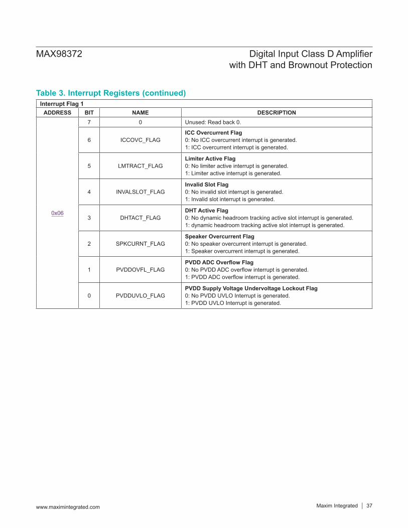
Table 3. Interrupt Registers (continued)Interrupt Flag 1
ADDRESS BIT NAME DESCRIPTION
0x06
7 0 Unused: Read back 0.
6 ICCOVC_FLAGICC Overcurrent Flag0: No ICC overcurrent interrupt is generated.1: ICC overcurrent interrupt is generated.
5 LMTRACT_FLAGLimiter Active Flag0: No limiter active interrupt is generated.1: Limiter active interrupt is generated.
4 INVALSLOT_FLAGInvalid Slot Flag 0: No invalid slot interrupt is generated.1: Invalid slot interrupt is generated.
3 DHTACT_FLAGDHT Active Flag0: No dynamic headroom tracking active slot interrupt is generated.1: dynamic headroom tracking active slot interrupt is generated.
2 SPKCURNT_FLAGSpeaker Overcurrent Flag0: No speaker overcurrent interrupt is generated.1: Speaker overcurrent interrupt is generated.
1 PVDDOVFL_FLAGPVDD ADC Overflow Flag 0: No PVDD ADC overflow interrupt is generated.1: PVDD ADC overflow interrupt is generated.
0 PVDDUVLO_FLAGPVDD Supply Voltage Undervoltage Lockout Flag0: No PVDD UVLO Interrupt is generated.1: PVDD UVLO Interrupt is generated.
www.maximintegrated.com Maxim Integrated 37
MAX98372 Digital Input Class D Amplifier with DHT and Brownout Protection
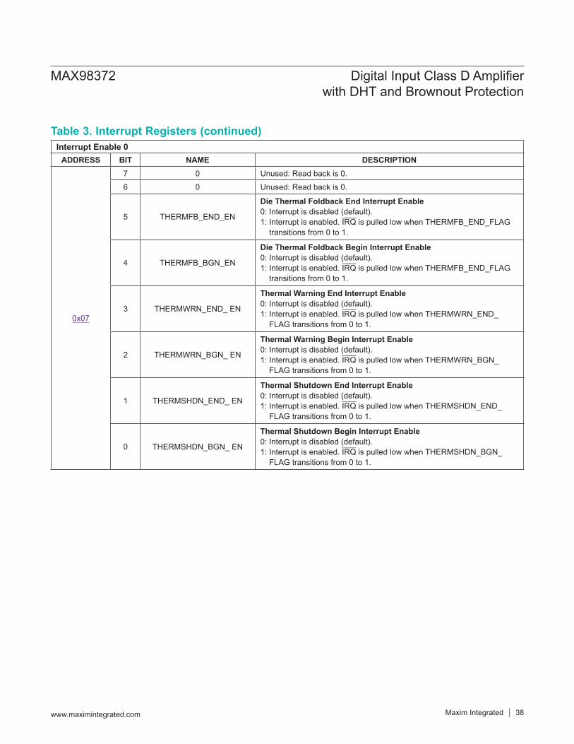
Table 3. Interrupt Registers (continued)Interrupt Enable 0
ADDRESS BIT NAME DESCRIPTION
0x07
7 0 Unused: Read back is 0.6 0 Unused: Read back is 0.
5 THERMFB_END_EN
Die Thermal Foldback End Interrupt Enable0: Interrupt is disabled (default).1: Interrupt is enabled. IRQ is pulled low when THERMFB_END_FLAG transitions from 0 to 1.
4 THERMFB_BGN_EN
Die Thermal Foldback Begin Interrupt Enable0: Interrupt is disabled (default).1: Interrupt is enabled. IRQ is pulled low when THERMFB_END_FLAG transitions from 0 to 1.
3 THERMWRN_END_ EN
Thermal Warning End Interrupt Enable0: Interrupt is disabled (default).1: Interrupt is enabled. IRQ is pulled low when THERMWRN_END_ FLAG transitions from 0 to 1.
2 THERMWRN_BGN_ EN
Thermal Warning Begin Interrupt Enable0: Interrupt is disabled (default).1: Interrupt is enabled. IRQ is pulled low when THERMWRN_BGN_ FLAG transitions from 0 to 1.
1 THERMSHDN_END_ EN
Thermal Shutdown End Interrupt Enable0: Interrupt is disabled (default).1: Interrupt is enabled. IRQ is pulled low when THERMSHDN_END_ FLAG transitions from 0 to 1.
0 THERMSHDN_BGN_ EN
Thermal Shutdown Begin Interrupt Enable0: Interrupt is disabled (default).1: Interrupt is enabled. IRQ is pulled low when THERMSHDN_BGN_ FLAG transitions from 0 to 1.
www.maximintegrated.com Maxim Integrated 38
MAX98372 Digital Input Class D Amplifier with DHT and Brownout Protection

Table 3. Interrupt Registers (continued)Interrupt Enable 1
ADDRESS BIT NAME DESCRIPTION
0x08
7 0 Unused: Read back is 0.
6 ICCOVC_EN
ICC Overcurrent Enable0: Interrupt is disabled (default).1: Interrupt is enabled. IRQ is pulled low when ICCOVC_FLAG transitions from 0 to 1.
5 LMTRACT_EN
Limiter Active Interrupt Enable0: Interrupt is disabled (default).1: Interrupt is enabled. IRQ is pulled low when LMTRACT_FLAG transitions from 0 to 1.
4 INVALSLOT_EN
Invalid Slot Interrupt Enable0: Interrupt is disabled (default).1: Interrupt enabled. IRQ is pulled low when INVALSLOT_FLAG transitions from 0 to 1.
3 DHTACT_EN
DHT Active Interrupt Enable0: Interrupt is disabled (default).1: Interrupt is enabled. IRQ is pulled low when DHTACT_FLAG transitions from 0 to 1.
2 SPKCURNT_EN
Speaker Overcurrent Interrupt Enable0: Interrupt is disabled (default).1: Interrupt is enabled. IRQ is pulled low when SPKCURNT_FLAG transitions from 0 to 1.
1 PVDDOVFL_EN
PVDD ADC Overflow Interrupt Enable0: Interrupt is disabled (default).1: Interrupt is enabled. IRQ is pulled low when PVDDOVFL_FLAG transitions from 0 to 1.
0 PVDDUVLO_EN
PVDD Supply Voltage Undervoltage Lockout Interrupt Enable0: Interrupt is disabled (default).1: Interrupt is enabled. IRQ is pulled low when PVDDUVLO_FLAG transitions from 0 to 1.
www.maximintegrated.com Maxim Integrated 39
MAX98372 Digital Input Class D Amplifier with DHT and Brownout Protection

Table 3. Interrupt Registers (continued)Interrupt Clear 0
ADDRESS BIT NAME DESCRIPTION
0x09
7 0 Unused: Read back is 0.6 0 Unused: Read back is 0.
5 THERMFB_END_CLRDie Thermal Foldback End Interrupt Clear0: No effect.1: Clears the THERMFB_END_STATE and THERMFB_END_FLAG.
4 THERMFB_BGN_CLRDie Thermal Foldback Begin Interrupt Clear0: No effect.1: Clears the THERMFB_BGN_STATE and THERMFB_BGN_FLAG.
3 THERMWRN_END_CLRThermal Warning End Interrupt Clear0: No effect.1: Clears the THERMWRN_END_STATE and THERMWRN_END_FLAG.
2 THERMWRN_BGN_CLRThermal Warning Begin Interrupt Clear0: No effect.1: Clears the THERMWRN_BGN_STATE and THERMWRN_BGN_FLAG.
1 THERMSHDN_END_CLRThermal Shutdown End Interrupt Clear0: No effect.1: Clears the THERMSHDN_END_STATE and THERMSHDN_END_FLAG.
0 THERMSHDN_BGN_CLRThermal Shutdown Begin Interrupt Clear0: No effect.1: Clears the THERMSHDN_BGN_STATE and THERMSHDN_BGN_FLAG.
www.maximintegrated.com Maxim Integrated 40
MAX98372 Digital Input Class D Amplifier with DHT and Brownout Protection

Table 3. Interrupt Registers (continued)Interrupt Clear 1
ADDRESS BIT NAME DESCRIPTION
0x0A
7 0 Unused: Read back is 0.
6 ICCOVC_CLRICC Overcurrent Clear0: No effect.1: Clears the ICCOVC_STATE and ICCOVC_FLAG.
5 LMTRACT_CLRLimiter Active Interrupt Clear0: No effect.1: Clears the LMTRACT_STATE and LMTRACT_FLAG.
4 INVALSLOT_CLRInvalid Slot Interrupt Clear0: No effect.1: Clears the INVALSLOT_STATE and INVALSLOT_FLAG.
3 DHTACT_CLRDHT Active Interrupt Clear0: No effect.1: Clears the DHTACT_STATE and DHTACT_FLAG.
2 SPKCURNT_CLRSpeaker Overcurrent Interrupt Clear0: No effect.1: Clears the SPKCURNT_STATE and SPKCURNT_FLAG.
1 PVDDOVFL_CLRPVDD ADC Overflow Interrupt Clear0: No effect.1: Clears the PVDDOVFL_STATE and PVDDOVFL_FLAG.
0 PVDDUVLO_CLRPVDD Supply Voltage Undervoltage Lockout Interrupt Clear0: No effect.1: Clears the PVDDUVLO_STATE and PVDDUVLO_FLAG.
Live Status 1ADDRESS BIT NAME DESCRIPTION
0x0B
7 0 Unused: Read back 0.6 0 Unused: Read back 0.5 0 Unused: Read back 0.4 0 Unused: Read back 0.
3 ALCINFH_STATUSALC Infinite Hold Event 0: ALC is not in infinite hold state1: ALC is in infinite hold state
2 ALCACT_STATUSALC Active Status 0: ALC is not reducing the gain of the PGA1: ALC is reducing the gain of the PGA due to low battery event
1 ALCMUT_STATUSALC Mute Status 0: ALC has not muted the audio path1: ALC has muted the audio path
0 0 Unused: Read back 0.
www.maximintegrated.com Maxim Integrated 41
MAX98372 Digital Input Class D Amplifier with DHT and Brownout Protection

Table 3. Interrupt Registers (continued)State 1
ADDRESS BIT NAME DESCRIPTION
0x0C
7 0 Unused: Read back is 0.
6 0 Unused: Read back is 0.
5 0 Unused: Read back is 0.
4 0 Unused: Read back is 0.
3 ALCINFH_STATEALC Infinite Hold Event 0: No rising edge on ALCINFH_STATUS is detected.1: A rising edge on ALCINFH_STATUS is detected.
2 ALCACT_STATEALC Activated Event 0: No rising edge on ALCACT_STATUS is detected.1: A rising edge on ALCACT_STATUS is detected.
1 ALCMUT_STATEALC Mute Event 0: No rising edge on ALCMUT_STATUS is detected.1: A rising edge on ALCMUT_STATUS is detected.
0 0 Unused: Read back is 0.Flag 1
ADDRESS BIT NAME DESCRIPTION
0x0D
7 0 Unused: Read back is 0.6 0 Unused: Read back is 0.5 0 Unused: Read back is 0.4 0 Unused: Read back is 0.
3 ALCINFH_FLAGALC Infinite Hold Flag 0: No interrupt generated.1: Interrupt generated.
2 ALCACT_FLAGALC Activated Flag 0: No interrupt generated.1: Interrupt generated.
1 ALCMUT_FLAGALC Mute Flag 0: No interrupt generated.1: Interrupt generated.
0 0 Unused: Read back is 0.
www.maximintegrated.com Maxim Integrated 42
MAX98372 Digital Input Class D Amplifier with DHT and Brownout Protection

Table 3. Interrupt Registers (continued)IRQ Enable 1
ADDRESS BIT NAME DESCRIPTION
0x0E
7 0 Unused: Read back is 0.6 0 Unused: Read back is 0.5 0 Unused: Read back is 0.4 0 Unused: Read back is 0.
3 ALCINFH_EN
ALC Infinite Hold Interrupt Enable 0: Interrupt disabled (default)1: Interrupt enabled. IRQ is pulled low when ALCINFH transitions from 0 to 1.
2 ALCACT_EN
ALC Activated Interrupt Enable 0: Interrupt disabled (default)1: Interrupt enabled. IRQ is pulled low when ALCACT transitions from 0 to 1.
1 ALCMUT_EN
ALC Mute Interrupt Enable 0: No interrupt generated (default)1: Interrupt enabled. IRQ is pulled low when ALCMUT transitions from 0 to 1.
0 0 Unused: Read back is 0.
IRQ Clear 1ADDRESS BIT NAME DESCRIPTION
0x0F
7 0 Unused: Read back is 0.6 0 Unused: Read back is 0.5 0 Unused: Read back is 0.4 0 Unused: Read back is 0.
3 ALCINFH_CLRClear ALC Infinite Hold Interrupt 0: No effect1: Clears ALCFINH_STATE and ALCINFH_FLAG
2 ALCACT_CLRClear ALC Activated Interrupt 0: No effect1: Clears ALCACT_STATE and ALCACT_FLAG
1 ALCMUT_CLRClear ALC Mute Interrupt 0: No effect1: Clears ALCMUT_STATE and ALCMUT_FLAG
0 0 Unused: Read back is 0.
www.maximintegrated.com Maxim Integrated 43
MAX98372 Digital Input Class D Amplifier with DHT and Brownout Protection
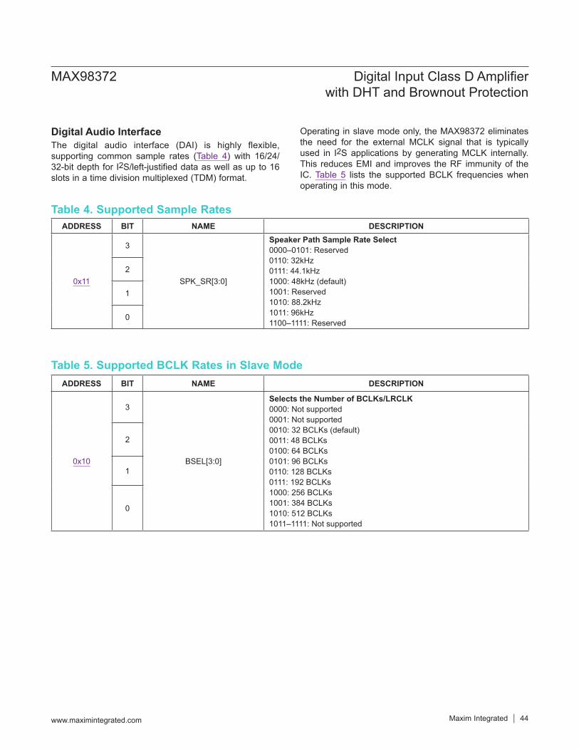
Digital Audio InterfaceThe digital audio interface (DAI) is highly flexible, supporting common sample rates (Table 4) with 16/24/ 32-bit depth for I2S/left-justified data as well as up to 16 slots in a time division multiplexed (TDM) format.
Operating in slave mode only, the MAX98372 eliminates the need for the external MCLK signal that is typically used in I2S applications by generating MCLK internally. This reduces EMI and improves the RF immunity of the IC. Table 5 lists the supported BCLK frequencies when operating in this mode.
Table 4. Supported Sample Rates
Table 5. Supported BCLK Rates in Slave Mode
ADDRESS BIT NAME DESCRIPTION
0x11
3
SPK_SR[3:0]
Speaker Path Sample Rate Select0000–0101: Reserved0110: 32kHz0111: 44.1kHz1000: 48kHz (default)1001: Reserved1010: 88.2kHz1011: 96kHz1100–1111: Reserved
2
1
0
ADDRESS BIT NAME DESCRIPTION
0x10
3
BSEL[3:0]
Selects the Number of BCLKs/LRCLK0000: Not supported0001: Not supported0010: 32 BCLKs (default)0011: 48 BCLKs0100: 64 BCLKs0101: 96 BCLKs0110: 128 BCLKs0111: 192 BCLKs1000: 256 BCLKs1001: 384 BCLKs1010: 512 BCLKs1011–1111: Not supported
2
1
0
www.maximintegrated.com Maxim Integrated 44
MAX98372 Digital Input Class D Amplifier with DHT and Brownout Protection

Interface FormatThe MAX98372 supports standard I2S, left-justified, and TDM data formats. I2S and left-justified formats support two audio channels of 16-, 24- or 32-bit depth. TDM supports up to 16 audio channels of 16-, 24-, or 32-bit depth. The IC supports slave operation only, and the LRCLK and BCLK pins operate as inputs.I2S (Figure 5) and left-justified (Figure 6) modes configure the LRCLK signal to transition before each channel. With the default I2S settings LRCLK low indicates left channel while LRCLK high indicates the right channel. The MSB of the audio word is latched on the second active BCLK edge after an LRCLK transition. In left-justified mode, the MSB of the audio word is latched on the first active BCLK edge after an LRCLK transition.
TDM mode (Figure 7) uses a frame sync pulse instead of a 50% duty cycle frame clock. The frame sync pulse (applied to the LRCLK pin) is equal to one BCLK period as a minimum, although the interface operates with longer periods; the rising edge of LRCLK is used to indicate the start of a new frame. The falling edge can occur at any time as long as it does not violate the setup time requirements of the LRCLK rising edge. In TDM, latch the MSB of the first audio word on the first or second active BCLK edge after an LRCLK rising edge.
Configuring the DAI FormatSpecify the format by configuring the LRCLK invert, BCLK active edge, data delay, and TDM mode configuration bits (Table 6).
Table 6. Configuration for Digital Audio Interface FormatADDRESS BIT NAME DESCRIPTION
0x14
7CHANSZ[1:0]
Configures Channel Word Length00: 8 bits 10: 24 bits (default)01: 16 bits 11: 32 bits6
5
FORMAT[2:0]
PCM Format Select000: I2S mode (default)001: Left-justified010: Right-justified011: TDM mode 1100: TDM mode 2101–111: Reserved
4
3
2 BCLEDGEActive BCLK Edge Select0: Data captured and valid on rising edge of BCLK (default)1: Data captured and valid on the falling edge of BCLK
1 CHANSEL
Non-TDM LRCLK Starting Edge0: Falling LRCLK indicates the start of a stereo pair. Channel 0 when LRCLK is low, channel 1 when LRCLK is high. (default)1: Rising LRCLK indicates the start of a stereo pair. Channel 0 when LRCLK is high, channel 1 when LRCLK is low.
0 0 Unused: Read back is 0.
www.maximintegrated.com Maxim Integrated 45
MAX98372 Digital Input Class D Amplifier with DHT and Brownout Protection
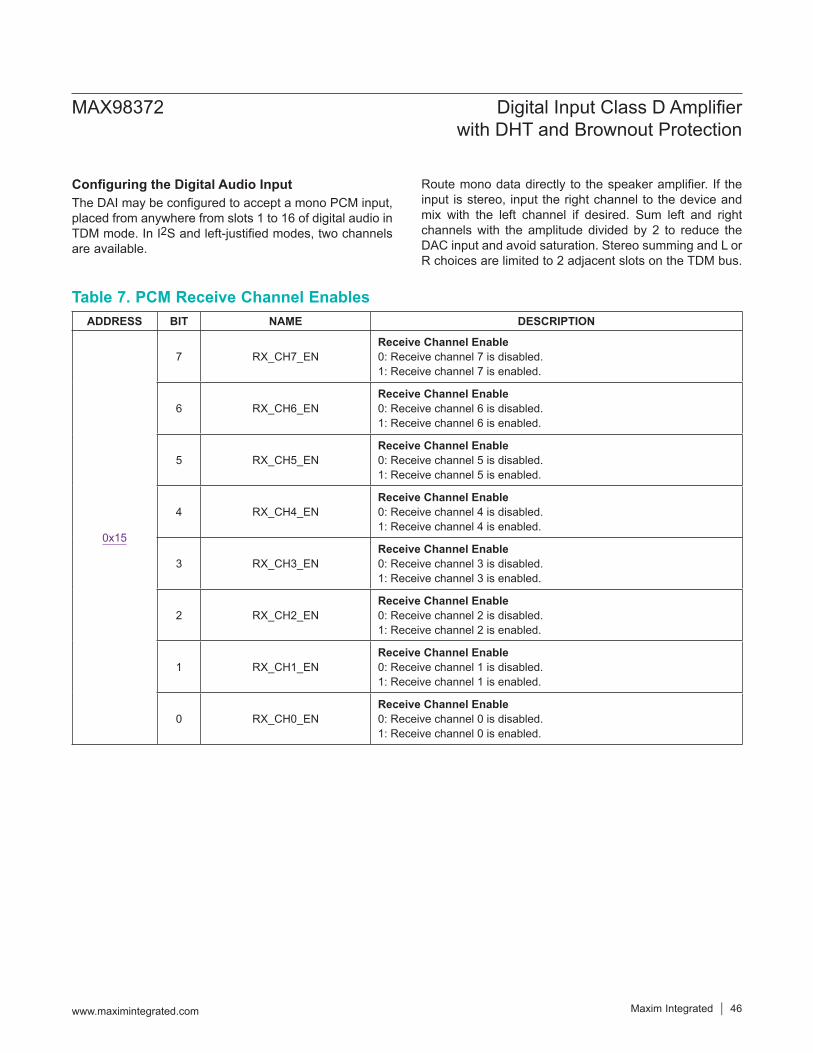
Configuring the Digital Audio InputThe DAI may be configured to accept a mono PCM input, placed from anywhere from slots 1 to 16 of digital audio in TDM mode. In I2S and left-justified modes, two channels are available.
Route mono data directly to the speaker amplifier. If the input is stereo, input the right channel to the device and mix with the left channel if desired. Sum left and right channels with the amplitude divided by 2 to reduce the DAC input and avoid saturation. Stereo summing and L or R choices are limited to 2 adjacent slots on the TDM bus.
Table 7. PCM Receive Channel EnablesADDRESS BIT NAME DESCRIPTION
0x15
7 RX_CH7_ENReceive Channel Enable0: Receive channel 7 is disabled.1: Receive channel 7 is enabled.
6 RX_CH6_ENReceive Channel Enable0: Receive channel 6 is disabled.1: Receive channel 6 is enabled.
5 RX_CH5_ENReceive Channel Enable0: Receive channel 5 is disabled.1: Receive channel 5 is enabled.
4 RX_CH4_ENReceive Channel Enable0: Receive channel 4 is disabled.1: Receive channel 4 is enabled.
3 RX_CH3_ENReceive Channel Enable0: Receive channel 3 is disabled.1: Receive channel 3 is enabled.
2 RX_CH2_ENReceive Channel Enable0: Receive channel 2 is disabled.1: Receive channel 2 is enabled.
1 RX_CH1_ENReceive Channel Enable0: Receive channel 1 is disabled.1: Receive channel 1 is enabled.
0 RX_CH0_ENReceive Channel Enable0: Receive channel 0 is disabled.1: Receive channel 0 is enabled.
www.maximintegrated.com Maxim Integrated 46
MAX98372 Digital Input Class D Amplifier with DHT and Brownout Protection
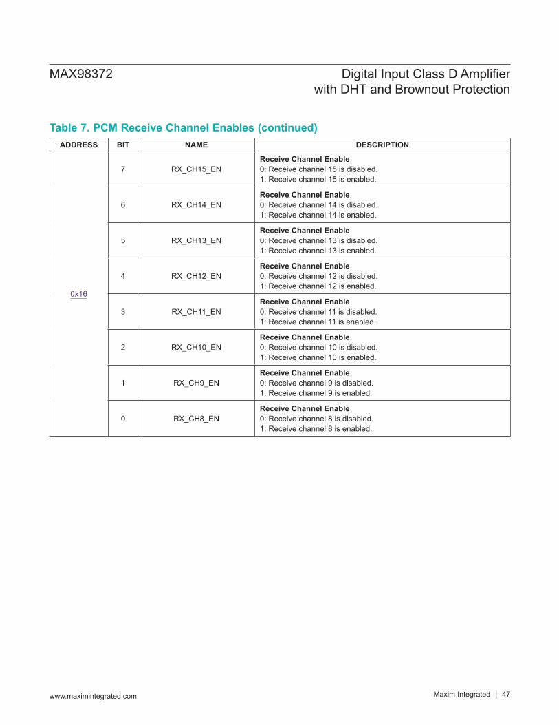
Table 7. PCM Receive Channel Enables (continued)ADDRESS BIT NAME DESCRIPTION
0x16
7 RX_CH15_ENReceive Channel Enable0: Receive channel 15 is disabled.1: Receive channel 15 is enabled.
6 RX_CH14_ENReceive Channel Enable0: Receive channel 14 is disabled.1: Receive channel 14 is enabled.
5 RX_CH13_ENReceive Channel Enable0: Receive channel 13 is disabled.1: Receive channel 13 is enabled.
4 RX_CH12_ENReceive Channel Enable0: Receive channel 12 is disabled.1: Receive channel 12 is enabled.
3 RX_CH11_ENReceive Channel Enable0: Receive channel 11 is disabled.1: Receive channel 11 is enabled.
2 RX_CH10_ENReceive Channel Enable0: Receive channel 10 is disabled.1: Receive channel 10 is enabled.
1 RX_CH9_ENReceive Channel Enable0: Receive channel 9 is disabled.1: Receive channel 9 is enabled.
0 RX_CH8_ENReceive Channel Enable0: Receive channel 8 is disabled.1: Receive channel 8 is enabled.
www.maximintegrated.com Maxim Integrated 47
MAX98372 Digital Input Class D Amplifier with DHT and Brownout Protection

Table 8. TDM Channel Selection for Mono Replay
Figure 5. I2S Digital Audio Format Examples
ADDRESS BIT NAME DESCRIPTION
0x18
7
DMONOMIX_CH1_SOURCE[3:0]
Digital Monomix Source Selection0000: Channel 1 gets PCM RX channel 0.0001: Channel 1 gets PCM RX channel 1.0010: Channel 1 gets PCM RX channel 2.0011: Channel 1 gets PCM RX channel 3.…1111: Channel 1 gets PCM RX channel 15.
6
5
4
3
DMONOMIX_CH0_SOURCE[3:0]
Digital Monomix Source Selection0000: Channel 0 gets PCM RX channel 0.0001: Channel 0 gets PCM RX channel 1.0010: Channel 0 gets PCM RX channel 2.0011: Channel 0 gets PCM RX channel 3.…1111: Channel 0 gets PCM RX channel 15.
2
1
0
0x19
1
DMONOMIX_CFG[1:0]
Monomix Configuration00: Output of Monomix is channel 0.01: Output of Monomix is channel 1.10: Output of Monomix is (channel 0 + channel 1)/2.11: Reserved
0
www.maximintegrated.com Maxim Integrated 48
MAX98372 Digital Input Class D Amplifier with DHT and Brownout Protection

Figure 6. Left-Justified Digital Audio Format Examples
www.maximintegrated.com Maxim Integrated 49
MAX98372 Digital Input Class D Amplifier with DHT and Brownout Protection
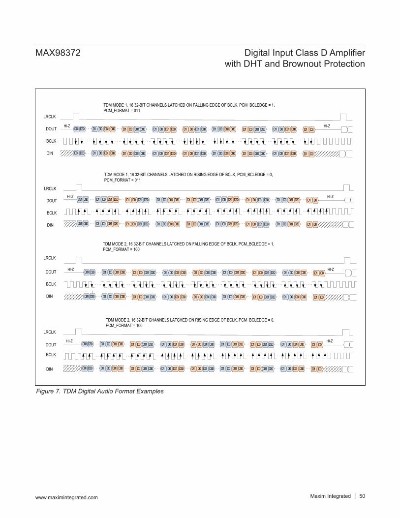
Figure 7. TDM Digital Audio Format Examples
TDM MODE 1, 16 32-BIT CHANNELS LATCHED ON FALLING EDGE OF BCLK, PCM_BCLEDGE = 1, PCM_FORMAT = 011
LRCLK
BCLK
DOUT D30 D1 D0 D31 D30
DIN
D31HI-ZHI-Z
D1 D0 D31 D30 D1 D0 D31 D30 D1 D0 D31 D30 D1 D0 D31 D30 D1 D0 D31 D30 D1 D0 D31 D30 D1 D0
D30 D1 D0 D31 D30D31 D1 D0 D31 D30 D1 D0 D31 D30 D1 D0 D31 D30 D1 D0 D31 D30 D1 D0 D31 D30 D1 D0 D31 D30 D1 D0
LRCLK
BCLK
DOUT D30 D1 D0 D31 D30
DIN
D31HI-ZHI-Z
D1 D0 D31 D30 D1 D0 D31 D30 D1 D0 D31 D30 D1 D0 D31 D30 D1 D0 D31 D30 D1 D0 D31 D30 D1 D0
D30 D1 D0 D31 D30D31 D1 D0 D31 D30 D1 D0 D31 D30 D1 D0 D31 D30 D1 D0 D31 D30 D1 D0 D31 D30 D1 D0 D31 D30 D1 D0
TDM MODE 1, 16 32-BIT CHANNELS LATCHED ON RISING EDGE OF BCLK, PCM_BCLEDGE = 0, PCM_FORMAT = 011
BCLK
DOUT D30 D1 D0 D31 D30
DIN
D31HI-ZHI-Z
D1 D0 D31 D30 D1 D0 D31 D30 D1 D0 D31 D30 D1 D0 D31 D30 D1 D0 D31 D30 D1 D0 D31 D30 D1 D0
D30 D1 D0 D31 D30D31 D1 D0 D31 D30 D1 D0 D31 D30 D1 D0 D31 D30 D1 D0 D31 D30 D1 D0 D31 D30 D1 D0 D31 D30 D1 D0
LRCLK
TDM MODE 2, 16 32-BIT CHANNELS LATCHED ON FALLING EDGE OF BCLK, PCM_BCLEDGE = 1, PCM_FORMAT = 100
LRCLK
BCLK
DOUT D30 D1 D0 D31 D30
DIN
D31HI-ZHI-Z
D1 D0 D31 D30 D1 D0 D31 D30 D1 D0 D31 D30 D1 D0 D31 D30 D1 D0 D31 D30 D1 D0 D31 D30 D1 D0
D30 D1 D0 D31 D30D31 D1 D0 D31 D30 D1 D0 D31 D30 D1 D0 D31 D30 D1 D0 D31 D30 D1 D0 D31 D30 D1 D0 D31 D30 D1 D0
TDM MODE 2, 16 32-BIT CHANNELS LATCHED ON RISING EDGE OF BCLK, PCM_BCLEDGE = 0, PCM_FORMAT = 100
www.maximintegrated.com Maxim Integrated 50
MAX98372 Digital Input Class D Amplifier with DHT and Brownout Protection

Digital Passband FilteringThe MAX98372 features an optional highpass filter with selectable corner frequency (50Hz, 100Hz, 200Hz, 400Hz, and 800Hz), or a DC-blocking filter with a cutoff frequency of 2Hz (80dB attenuation). The MAX98372 supports 5 sample rates: 32kHz, 44.1kHz, 48kHz, 88.2kHz, or 96KHz. For 32kHz, 44.1kHz, and 48kHz, a linear phase, half-band filter effectively defines the response. For 96kHz operation, a different filter characteristic is employed with a smooth roll off above 20kHz. Set the digital highpass filter corner frequency though the DACHPF bits in control register 0x1C (Table 9). Create user-programmed filtering
through the biquad filter coefficients by setting the DACHPF[2:0] bits to 111. See the Biquad Filter section.The MAX98372 also features a configurable PVDD ADC filter. This cutoff frequency of this filter can be adjusted by setting the PVDD_ADC_BW bits in register 0x1C. These filtered PVDD ADC measurements can be fed to the DHT or limiter. Filtered or unfiltered PVDD ADC readings can be sent to the DHT and limiter. To send filtered data to the limiter or DHT, set the PVDD_FILT_TO_LMTR or PVDD_FILT_TO_DHT bits, respectively. See Table 9.
Table 9. Digital Highpass FilterADDRESS BIT NAME DESCRIPTION
0x1C
7 PVDD_FILT_TO_LMTR 0: Unfiltered PVDD ADC measurements are sent to the limiter.1: Lowpass filtered PVDD ADC measurements are sent to limiter.
6 PVDD_FILT_TO_DHT 0: Unfiltered PVDD ADC measurements are sent to DHT.1: Lowpass filtered PVDD ADC measurements are sent to DHT.
5PVDD_ADC_BW[1:0]
PVDD ADC Lowpass Filter Selection00: Pass through, filter off01: 2Hz cutoff10: 20Hz cutoff11: 200Hz cutoff
4
3 0 Unused: Read back is 0.
2
DACHPF[2:0]
Digital Highpass Filter000: Pass through, filter off001: DC blocker is enabled.010: 50Hz HPF is enabled.011: 100Hz HPF is enabled.100: 200Hz HPF is enabled.101: 400Hz HPF is enabled.110: 800Hz HPF is enabled.111: User programmable using DAC_BQ_B[0–2] and DAC_BQ_A[1–2] registers
1
0
www.maximintegrated.com Maxim Integrated 51
MAX98372 Digital Input Class D Amplifier with DHT and Brownout Protection
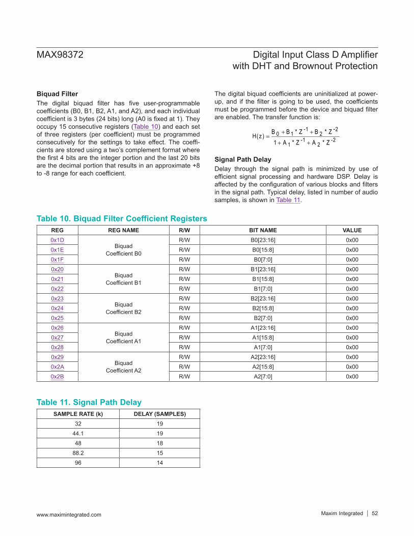
Biquad FilterThe digital biquad filter has five user-programmable coefficients (B0, B1, B2, A1, and A2), and each individual coefficient is 3 bytes (24 bits) long (A0 is fixed at 1). They occupy 15 consecutive registers (Table 10) and each set of three registers (per coefficient) must be programmed consecutively for the settings to take effect. The coeffi-cients are stored using a two’s complement format where the first 4 bits are the integer portion and the last 20 bits are the decimal portion that results in an approximate +8 to -8 range for each coefficient.
The digital biquad coefficients are uninitialized at power-up, and if the filter is going to be used, the coefficients must be programmed before the device and biquad filter are enabled. The transfer function is:
+ +=
+ +
-1 20 1 2
-1 -21 2
-B B * Z B * ZH(z )1 A * Z A * Z
Signal Path DelayDelay through the signal path is minimized by use of efficient signal processing and hardware DSP. Delay is affected by the configuration of various blocks and filters in the signal path. Typical delay, listed in number of audio samples, is shown in Table 11.
Table 11. Signal Path Delay
Table 10. Biquad Filter Coefficient RegistersREG REG NAME R/W BIT NAME VALUE0x1D
BiquadCoefficient B0
R/W B0[23:16] 0x000x1E R/W B0[15:8] 0x000x1F R/W B0[7:0] 0x000x20
BiquadCoefficient B1
R/W B1[23:16] 0x000x21 R/W B1[15:8] 0x000x22 R/W B1[7:0] 0x000x23
BiquadCoefficient B2
R/W B2[23:16] 0x000x24 R/W B2[15:8] 0x000x25 R/W B2[7:0] 0x000x26
BiquadCoefficient A1
R/W A1[23:16] 0x000x27 R/W A1[15:8] 0x000x28 R/W A1[7:0] 0x000x29
BiquadCoefficient A2
R/W A2[23:16] 0x000x2A R/W A2[15:8] 0x000x2B R/W A2[7:0] 0x00
SAMPLE RATE (k) DELAY (SAMPLES)32 19
44.1 1948 18
88.2 1596 14
www.maximintegrated.com Maxim Integrated 52
MAX98372 Digital Input Class D Amplifier with DHT and Brownout Protection
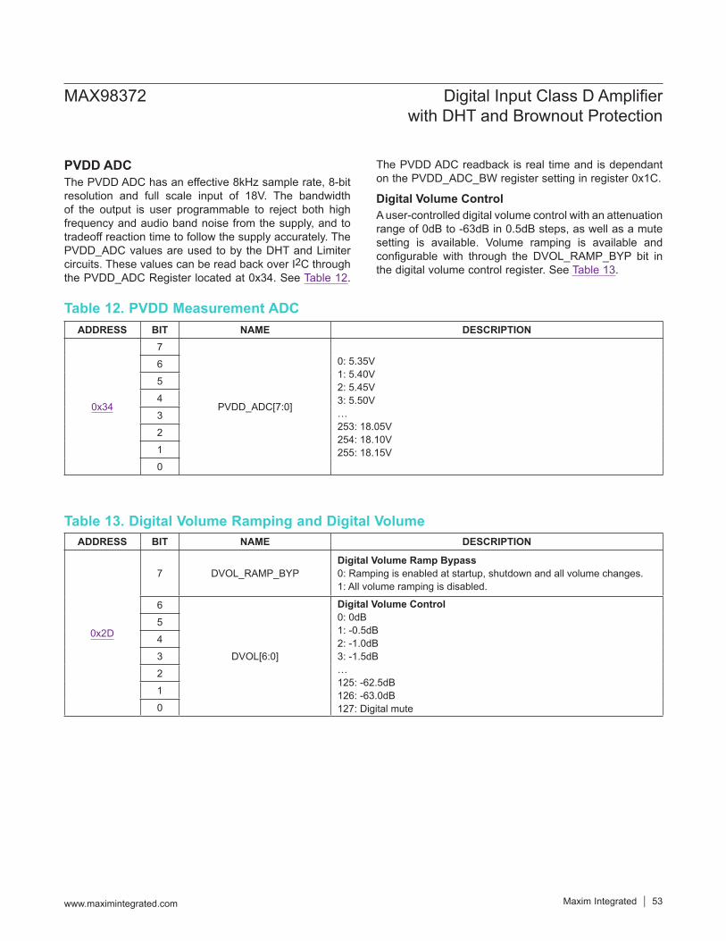
PVDD ADCThe PVDD ADC has an effective 8kHz sample rate, 8-bit resolution and full scale input of 18V. The bandwidth of the output is user programmable to reject both high frequency and audio band noise from the supply, and to tradeoff reaction time to follow the supply accurately. The PVDD_ADC values are used to by the DHT and Limiter circuits. These values can be read back over I2C through the PVDD_ADC Register located at 0x34. See Table 12.
The PVDD ADC readback is real time and is dependant on the PVDD_ADC_BW register setting in register 0x1C.
Digital Volume ControlA user-controlled digital volume control with an attenuation range of 0dB to -63dB in 0.5dB steps, as well as a mute setting is available. Volume ramping is available and configurable with through the DVOL_RAMP_BYP bit in the digital volume control register. See Table 13.
Table 12. PVDD Measurement ADC
Table 13. Digital Volume Ramping and Digital Volume
ADDRESS BIT NAME DESCRIPTION
0x34
7
PVDD_ADC[7:0]
0: 5.35V1: 5.40V2: 5.45V3: 5.50V…253: 18.05V254: 18.10V255: 18.15V
6543210
ADDRESS BIT NAME DESCRIPTION
0x2D
7 DVOL_RAMP_BYPDigital Volume Ramp Bypass0: Ramping is enabled at startup, shutdown and all volume changes.1: All volume ramping is disabled.
6
DVOL[6:0]
Digital Volume Control0: 0dB1: -0.5dB2: -1.0dB3: -1.5dB…125: -62.5dB126: -63.0dB127: Digital mute
543210
www.maximintegrated.com Maxim Integrated 53
MAX98372 Digital Input Class D Amplifier with DHT and Brownout Protection

Output Voltage ScalingThe MAX98372 operates over a large supply voltage range. As a result, the part must be configured to scale the output signals across possible PVDD supply range. SPK_GAIN_MAX applies gain after the DAC to achieve this voltage scaling.Digital gain can be applied before the DAC by using the DPGA_CLIP register. In conjunction with the SPK_GAIN_MAX setting, the overall full-scale behavior of the device is set.
The DPGA and SPK_GAIN_MAX register settings are shown in Table 14.Gain through the signal path is referenced to the full-scale output of the DAC, which is 2.1dBV. The MAX98372 output level can be calculated based on the digital input signal level and selected amplifier gain.
Output signal level (dBV) = input signal level (dBFS) + 2.1dBV + SPK_GAIN_MAX (dB)
where 0dBFS is referenced to 0dBV.
Table 14. Digital Gain Settings and Output Voltage ScalingADDRESS BIT NAME DESCRIPTION
0x2E
7
DPGA_CLIP[3:0]
Digital Gain Settings (dB)0000: 0 0110: 3.00001: 0.5 0111: 3.50010: 1.0 1000: 4.00011: 1.5 1001: 5.00100: 2.0 1010: 6.00101: 2.5 1011–1111: 0
6
5
4
3
SPK_GAIN_MAX[3:0]
Speaker No-Load Output Voltage MaximumSets the output voltage level (VP) of 0dBFS.0000: 5.37 (9.5dB) Guaranteed no clipping0001: 6.03 (10.5dB) Best near 5.5V (min) operating0010: 6.77 (11.5dB) 0011: 7.59 (12.5dB) 0100: 8.52 (13.5dB) 2-cell Li-ion operation0101: 9.56 (14.5dB) 0110: 10.72 (15.5dB) 0111: 12.03 (16.5dB) 12V nominal1000: 13.5 (17.5dB) 3-cell Li-ion operation1001: 15.15 (18.5dB)1010: 16.99 (19.5dB) Optimum for 16.5V PVDD operation1011: 19.07 (20.5dB)1100–1111: Reserved
2
1
0
www.maximintegrated.com Maxim Integrated 54
MAX98372 Digital Input Class D Amplifier with DHT and Brownout Protection
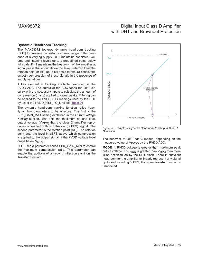
Dynamic Headroom TrackingThe MAX98372 features dynamic headroom tracking (DHT) to preserve consistant dynamic range in the pres-ence of a varying supply. DHT maintains consistent vol-ume and listening levels up to a predefined point, below full scale. DHT maintains the headroom of the amplifier at signal peaks that occur above this level (referred to as the rotation point or RP) up to full scale to ensure consistent, smooth compression of these signals in the presence of supply variations.A key element in tracking available headroom is the PVDD ADC. The output of the ADC feeds the DHT cir-cuitry with the necessary inputs to calculate the amount of compression (if any) applied to signal peaks. Filtering can be applied to the PVDD ADC readings used by the DHT by using the PVDD_FILT_TO_DHT bit (Table 9).The dynamic headroom tracking function relies heav-ily on two parameters to be effective. The first is the SPK_GAIN_MAX setting explained in the Output Voltage Scaling section. This sets the maximum no-load peak output voltage (VMPO) that the class D amplifier repro-duces when fed with a full-scale (0dBFS) signal. The second parameter is the rotation point (RP). The rotation point sets the level in dBFS above which compression is applied to the output signal, if the PVDD voltage level drops below VMPO.DHT uses a parameter called SPK_GAIN_MIN to control the maximum compression ratio. This parameter can enable the addition of a second inflection point on the Transfer function.
The behavior of DHT has 3 modes, depending on the measured value of VPVDD by the PVDD ADC:MODE 1: PVDD voltage is greater than maximum peak output voltage. If VPVDD is greater than VMPO then there is no action taken by the DHT block. There is sufficient headroom for the amplifier to linearly represent any signal up to and including 0dBFS; the signal transfer function is unaffected.
Figure 8. Example of Dynamic Headroom Tracking in Mode 1 Operation
VMPO
0-6
ROTATION POINT (RP) SET BY USER
OUTP
UT V
OLTA
GE LE
VEL (
V P)
INPUT SIGNAL LEVEL (dBFS)
PVDD > VMPO
VEXP_RP
www.maximintegrated.com Maxim Integrated 55
MAX98372 Digital Input Class D Amplifier with DHT and Brownout Protection

MODE 2: VPVDD is less than VMPO, and greater than the output voltage as set by the Rotation Point register set-ting (VEXP_RP). For example, if the RP is set for -6dBFS, then the peak voltage on the output (VEXP_RP) would be VMPO/2). If this is the case, the transfer function for signals below the RP is reproduced exactly as in Mode 1. Any signals between RP and 0dBFS are now subject to an audio compression function, acting in the DSP block of the MAX98372. This acts with appropriate attenuation for peaks over the RP in magnitude with programmable attack and release times (see the DHT Ballistics section). Figure 9 and Figure 10 show the effect on the transfer function.The compression ratios in Mode 2 are effectively defined by the combination of: PVDD, RP, SPK_GAIN_MAX, and SPK_GAIN_MIN settings. The ballistics of the compressor
(in both Mode 2 and Mode 3) are set by the parameters in Table 16 and Figure 21.MODE 3a: PVDD voltage is less than the rotation points maximum output voltage, VEXP_RP. When the rotation point is set to a high value (for example -6dBFS) this mode applies. If VPVDD is less than VEXP_RP, then hard limiting is applied to peaks and the effective RP is now set by the need to fit peak signals into the available PVDD range. The MAX98372 automatically determines a new RP based on the PVDD ADC. Normally, RP is set so that this mode is never used, and the VEXP_RP as set by the RP and SPK_GAIN_MAX combination should reflect the lowest PVDD value expected. In this mode, the SPK_GAIN_MIN parameter is set to be well below the VEXP_RP.
Figure 9. Example of Dynamic Headroom Tracking in Mode 2 Operation with a High RP
VMPO
INPUT (dBFS)0-6
VEXP_RP
PEAK OUTPUT SCALED TO FIT AVAILABLE PVDD
COMPRESSION RATIO IS SCALED TO FIT TRANSFER FUNCTION AUTOMATICALLY BETWEEN ROTATION POINT AND THEORETICAL PEAK OUTPUT VOLTAGE (AS DETERMINED BY PVDD ADC BLOCK)
DECR
EASI
NG P
VDD
OUTP
UT V
OLTA
GE LE
VEL (
V P)
INPUT SIGNAL LEVEL (dBFS)
PVDD < VMPO
RP S
ET B
Y US
ER
SPK_GAIN_MAX
www.maximintegrated.com Maxim Integrated 56
MAX98372 Digital Input Class D Amplifier with DHT and Brownout Protection
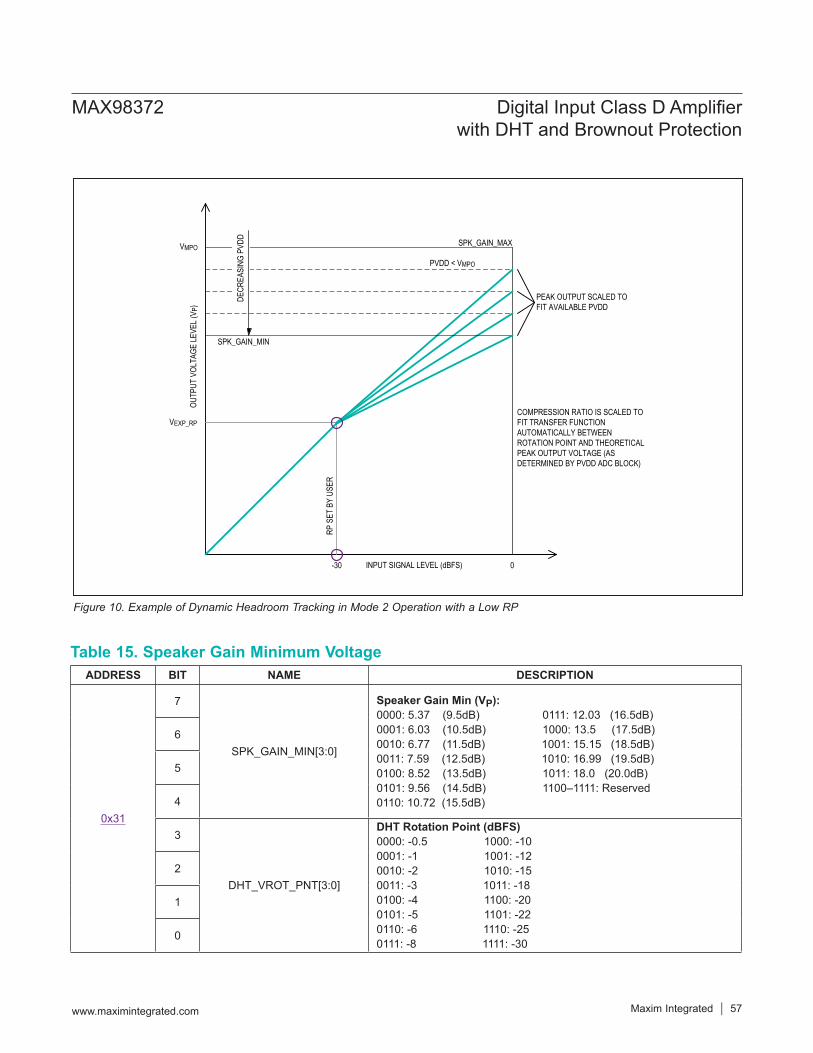
Table 15. Speaker Gain Minimum Voltage
Figure 10. Example of Dynamic Headroom Tracking in Mode 2 Operation with a Low RP
VMPO
0-30
VEXP_RP
PEAK OUTPUT SCALED TO FIT AVAILABLE PVDD
COMPRESSION RATIO IS SCALED TO FIT TRANSFER FUNCTION AUTOMATICALLY BETWEEN ROTATION POINT AND THEORETICAL PEAK OUTPUT VOLTAGE (AS DETERMINED BY PVDD ADC BLOCK)
DECR
EASI
NG P
VDD
PVDD < VMPO
OUTP
UT V
OLTA
GE LE
VEL (
V P)
INPUT SIGNAL LEVEL (dBFS)
RP S
ET B
Y US
ERSPK_GAIN_MIN
SPK_GAIN_MAX
ADDRESS BIT NAME DESCRIPTION
0x31
7
SPK_GAIN_MIN[3:0]
Speaker Gain Min (VP):0000: 5.37 (9.5dB) 0111: 12.03 (16.5dB)0001: 6.03 (10.5dB) 1000: 13.5 (17.5dB)0010: 6.77 (11.5dB) 1001: 15.15 (18.5dB)0011: 7.59 (12.5dB) 1010: 16.99 (19.5dB)0100: 8.52 (13.5dB) 1011: 18.0 (20.0dB) 0101: 9.56 (14.5dB) 1100–1111: Reserved0110: 10.72 (15.5dB)
6
5
4
3
DHT_VROT_PNT[3:0]
DHT Rotation Point (dBFS)0000: -0.5 1000: -100001: -1 1001: -120010: -2 1010: -150011: -3 1011: -180100: -4 1100: -200101: -5 1101: -220110: -6 1110: -250111: -8 1111: -30
2
1
0
www.maximintegrated.com Maxim Integrated 57
MAX98372 Digital Input Class D Amplifier with DHT and Brownout Protection

MODE 3b: PVDD voltage is less than the speaker gain minimum output voltage. When the rotation point is set to a low value (for example -30dBFS) this mode applies. If VPVDD is less than SPK_GAIN_MIN, the DHT cannot
compress the signal any further. So the compression ratio stays fixed, and as PVDD decreases below SPK_GAIN_MIN, the output signal starts to clip. This clipping can be eliminated if the limiter is enabled in addition to the DHT.
Figure 11. Example of Dynamic Headroom Tracking in Mode 3a Operation
VMPO
0-6
DECR
EASI
NG P
VDD
RP S
ET B
Y US
ER
OUTP
UT V
OLTA
GE LE
VEL (
V P)
INPUT SIGNAL LEVEL (dBFS)
VEXP_RP PVDD < VEXP_RP
WHEN PVDD < VEXP_RP A NEW ROTATION POINT IS AUTOMATICALLY DETERMINED AND INFINITE COMPRESSION IS APPLIED.
SPK_GAIN_MAX
www.maximintegrated.com Maxim Integrated 58
MAX98372 Digital Input Class D Amplifier with DHT and Brownout Protection
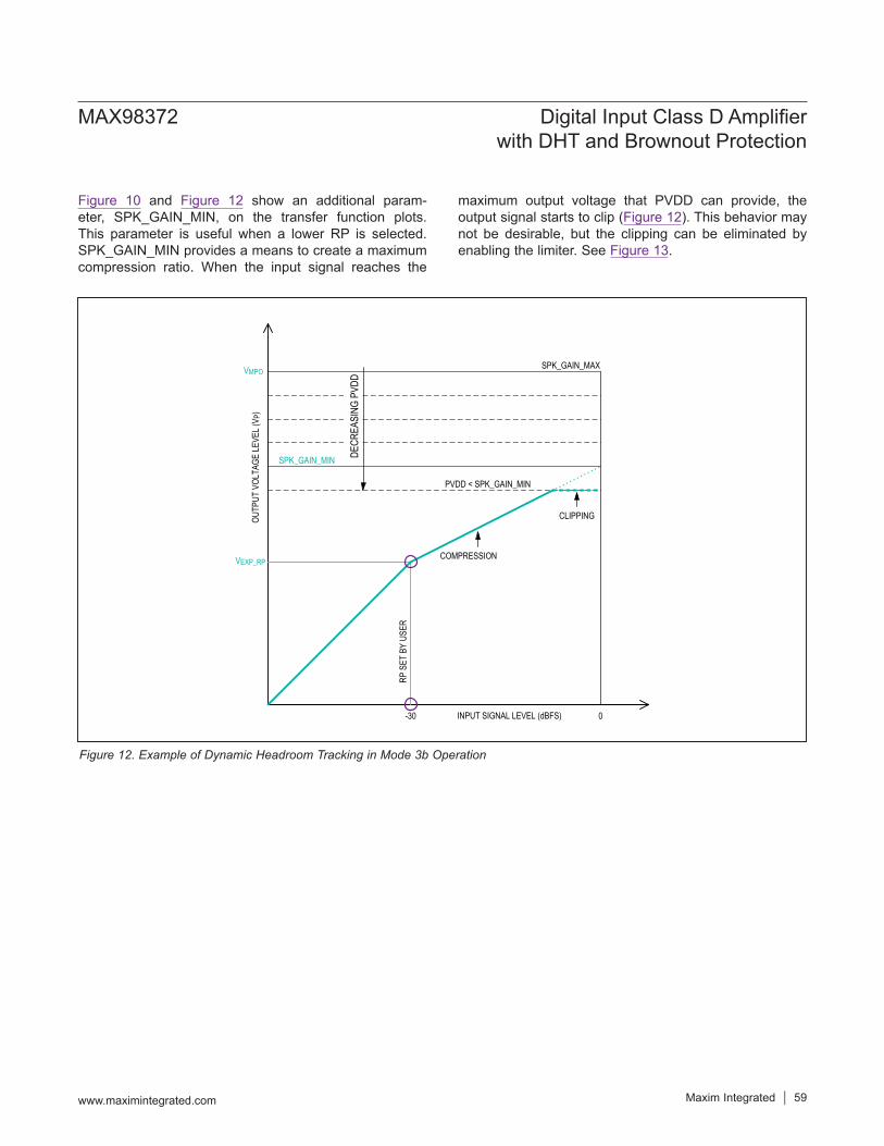
Figure 10 and Figure 12 show an additional param-eter, SPK_GAIN_MIN, on the transfer function plots. This parameter is useful when a lower RP is selected. SPK_GAIN_MIN provides a means to create a maximum compression ratio. When the input signal reaches the
maximum output voltage that PVDD can provide, the output signal starts to clip (Figure 12). This behavior may not be desirable, but the clipping can be eliminated by enabling the limiter. See Figure 13.
Figure 12. Example of Dynamic Headroom Tracking in Mode 3b Operation
VMPO
0-30
VEXP_RP
DECR
EASI
NG P
VDD
PVDD < SPK_GAIN_MIN
OUTP
UT V
OLTA
GE LE
VEL (
V P)
INPUT SIGNAL LEVEL (dBFS)
RP S
ET B
Y US
ER
SPK_GAIN_MIN
COMPRESSION
CLIPPING
SPK_GAIN_MAX
www.maximintegrated.com Maxim Integrated 59
MAX98372 Digital Input Class D Amplifier with DHT and Brownout Protection
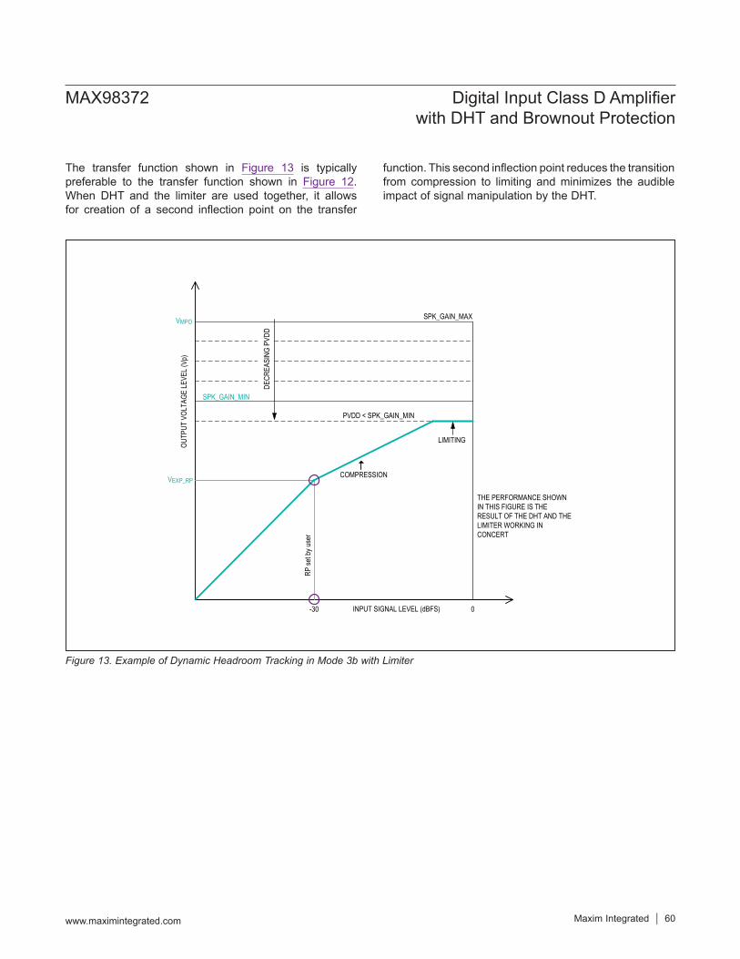
The transfer function shown in Figure 13 is typically preferable to the transfer function shown in Figure 12. When DHT and the limiter are used together, it allows for creation of a second inflection point on the transfer
function. This second inflection point reduces the transition from compression to limiting and minimizes the audible impact of signal manipulation by the DHT.
Figure 13. Example of Dynamic Headroom Tracking in Mode 3b with Limiter
VMPO
0-30
VEXP_RP
DECR
EASI
NG P
VDD
PVDD < SPK_GAIN_MIN
OUTP
UT V
OLTA
GE LE
VEL (
Vp)
INPUT SIGNAL LEVEL (dBFS)
RP se
t by u
ser
SPK_GAIN_MIN
COMPRESSION
LIMITING
THE PERFORMANCE SHOWN IN THIS FIGURE IS THE RESULT OF THE DHT AND THE LIMITER WORKING IN CONCERT
SPK_GAIN_MAX
www.maximintegrated.com Maxim Integrated 60
MAX98372 Digital Input Class D Amplifier with DHT and Brownout Protection

DHT BallisticsWhen an input signal exceeds the rotation point, DHT applies attenuation to the signal over some amount of time (this is configurable through the DHT_ATK_RATE register 0x32). The instant that the large signal is input to the MAX98372, the output tries to reproduce that signal without any attenuation from the DHT. Over time, the DHT applies compression to ensure that the signal can fit within the available PVDD voltage. If a large enough input signal is applied there can be hard clipping on the output for a short time (Figure 14). However, after the full attack time has completed, there should be no clipping. Hard clipping can also be prevented by using the limiter. See the Limiter section.
Observing the output waveform, notice that the amount of attenuation applied increases up to when VIN(dBFS) = PVDD (dBFS). Once VIN(dBFS) is greater than PVDD(dBFS) the amount of attenuation observed in the output waveform appears to decrease. This is a result of the output clipping against the PVDD voltage level. The DHT still takes the same amount of time to apply the compression as though it had the headroom to reproduce the signal.
The amount of compression applied by DHT depends on a few parameters: SPK_GAIN_MAX, PVDD, input signal amplitude, and the rotation point.
To establish where PVDD is relative to speaker gain max, use the following equation:
Figure 14. Dynamic Headroom Tracking Attack Functionality
VMPO
INPUT (dBFS)0-10
VEXP_RP
-3 dB
OUTP
UT V
OLTA
GE LE
VEL (
V P)
INPUT SIGNAL LEVEL (dBFS)
VPVDD = 8.4V
RP S
ET B
Y US
ER
SPK_GAIN_MAX
-3
ATTACK
THE ATTACK ARROW DEMOSTRATES THE TRANSISTION FROM AN UNATTENUATED SIGNAL
TO THE COMPRESSED SIGNAL THAT OCCURS OVER THE TOTAL
ATTACK TIME.
www.maximintegrated.com Maxim Integrated 61
MAX98372 Digital Input Class D Amplifier with DHT and Brownout Protection

Equation 1
M P O
P V D D( V )P V D D(dB FS ) 20logV
=
where PVDD(V) is the voltage readback from the PVDD ADC, and VMPO is the maximum peak output voltage (VMPO), see Figure 14. For example, if VPVDD = 12V and VMPO = 12V, then PVDD(dBFS) = 0dBFS. It should be noted that 0dBFS is the maximum value for PVDD(dBFS). If solving Equation 1 returns a value greater than 0 then 0dBFS should be used for further calculations. This is important as DHT only ever applies attenuation and never positive gain.If VPVDD = 8.4V and VSPK_GAIN_MAX = 12V, then solving Eq 1 gives -3.098dBFS. This is PVDD’s level relative to SPK_GAIN_MAX in dB. To find the expected compressed output voltage, use the following equation:Equation 2
= + ×
R P
-P V D D(dB FS )A T T E N U A T IO N(dB ) P V D D(dB FS ) Inpu t(dB FS )V (dB FS )
When PVDD(dBFS) = 0, the PVDD and the fraction term drop out, which gives attenuation equal to zero. This makes sense because when PVDD(dBFS) = 0, there is sufficient headroom to playback any signal input into the MAX98372 and no compression is applied.
A nontrivial case might be If VPVDD = 8.4V, VMPO = 12V, rotation point = -10dBFS, and the input signal level is -5dBFS. Next, we solve equation 3 with these values:Equation 3
= + ×
= + ×
=
R P
-P V D D(dB FS )P V D D(dB FS ) Inpu t(dB FS )V (dB FS )
3 .098dB FS-3 .098dB FS -5dB FS-10dB FS
-1 .54dB FSFor this example, the total amount of compression applied by DHT 1.54dB. DHT attack rate and DHT attack step can be configured to apply the 1.54dB of attenuation of over a programmable amount of time.As a rule of thumb, attack times (product of attack rate, attack step, and number of steps) faster than 600µs are not achievable. This is independent of sample rate. Input data is rectified, filtered and converted to the log domain. The DSP compares the input data with filtered data from the PVDD ADC then compression is applied within the DSP. The compressed data must be converted back to lin-ear scale and then output. The large number of complex computations required in the DSP requires a fixed 600µs to complete the compression algorithm. As a result, attack times faster than 600µs are not possible. See Table 16.Continuing the same example when the input signal size decreases below the rotation point DHT releases the 1.54dB of attenuation it applied to the signal. The release time for DHT is configurable through Register 0x33. See Table 17.
Table 16. Dynamic Headroom Tracking Attack SettingsADDRESS BIT NAME DESCRIPTION
0x32
4
DHT_ATK_STEP[1:0]
DHT Attack Step Size00: 0.25dB01: 0.5 dB10: 1.0dB11: 2.0dB (default)3
2
DHT_ATK_RATE[2:0]
DHT Compressor Attack RateAll attack times in µs/step000: 17.5 (default)001: 35010: 70011: 140100: 280101: 560110: 1120111: 2240
1
0
www.maximintegrated.com Maxim Integrated 62
MAX98372 Digital Input Class D Amplifier with DHT and Brownout Protection
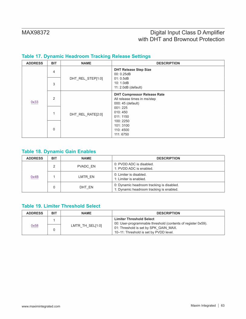
Table 19. Limiter Threshold Select
Table 17. Dynamic Headroom Tracking Release Settings
Table 18. Dynamic Gain EnablesADDRESS BIT NAME DESCRIPTION
0x4B
2 PVADC_EN 0: PVDD ADC is disabled.1: PVDD ADC is enabled.
1 LMTR_EN 0: Limiter is disabled.1: Limiter is enabled.
0 DHT_EN 0: Dynamic headroom tracking is disabled.1: Dynamic headroom tracking is enabled.
ADDRESS BIT NAME DESCRIPTION
0x581
LMTR_TH_SEL[1:0]
Limiter Threshold Select00: User-programmable threshold (contents of register 0x59).01: Threshold is set by SPK_GAIN_MAX.10–11: Threshold is set by PVDD level.
0
ADDRESS BIT NAME DESCRIPTION
0x33
4
DHT_REL_STEP[1:0]
DHT Release Step Size00: 0.25dB01: 0.5dB10: 1.0dB11: 2.0dB (default)
3
2
DHT_REL_RATE[2:0]
DHT Compressor Release RateAll release times in ms/step000: 45 (default)001: 225010: 450011: 1150100: 2250101: 3100110: 4500111: 6750
1
0
www.maximintegrated.com Maxim Integrated 63
MAX98372 Digital Input Class D Amplifier with DHT and Brownout Protection

LimiterThe MAX98372 features a programmable limiter that is used to compress large near full-scale signals. The input signal level where the attenuation is applied varies based on how the Limiter Threshold Select register is set.When LMTR_TH_SEL is set to 00, the limiter threshold is user configurable through register LMTR_THC. See Table 20.When LMTR_TH_SEL is set to 01, the threshold is determined by SPK_GAIN_MAX. Table 21 provides the threshold values.When LMTR_TH_SEL is set to 10 or 11, the part looks at the PVDD ADC and the SPK_GAIN_MAX setting and determines the maximum output swing that the part can deliver without clipping. Input signals that require more voltage than is available on PVDD are limited to prevent clipping. Filtering can be applied to the PVDD ADC read-ings used by the limiter with the PVDD_FILT_TO_LMTR bit (Table 9).The limiter attack and release rates are measured in abso-lute time and are independent of sample rate. The limiter has its own set of configurable ballistics (Figure 30).
Thermal ADCThe MAX98372 features a die temperature monitoring ADC. This 6-bit ADC with a 100kHz sample rate reports the die temperature from +100°C to +163°C. THRM_MIN_TEMP sets the temperature at which the thermal foldback circuit initially activates. The measurements from the thermal ADC can be filtered before they are used by the thermal foldback circuit, or the values can pass directly without being filtered. THRM_FILT_SEL controls the filter selection.
Thermal ProtectionThe MAX98372 continuously monitors die temperature to ensure that the temperature does not exceed the maxi-mum of +150°C (typ). The device can warn the host if die temperature is approaching the limit and turns off the speaker amplifier if the limit is exceeded. The interrupt registers are maintained to ensure that host is alerted of the overtemperature event. Thermal recovery behavior of the device is determined by the state of TDHSN_AUTO_RESTART bit in the Restart Behavior (0x4D) register. If TSHDN_AUTO_RESTART is reset, a drop in the die temperature below the thermal foldback threshold trig-gers an interrupt to the host, indicating that it is safe to turn on the speaker amplifier and resume audio playback. If TSHDN_AUTO_RESTART is set, the device will turn on the speaker amplifier when the die temperature drops below the thermal foldback threshold setting.
Thermal FoldbackTo allow a smoother audio response to high temperature events, the MAX98372 features a thermal foldback loop. As the die temperature rises above a threshold of set by THRM_MIN_TEMP register (+120°C by default), the audio path is subjected to increasing attenuation, up to a maximum of -12dB. See Table 23.
Table 20. Manual Limiter Threshold Settings
Table 21. Limiter Threshold
ADDRESS BIT NAME DESCRIPTION
0x59
4
LMTR_THC[4:0]
Manual Limiter Threshold Setting (Input Referred) 00000: 0dBFS00001: -1dBFS00010: -2dBFS00011: -3dBFS…11101: -29dBFS11110: -30dBFS11111: -31dBFS
3
2
1
0
SPK_GAIN_MAX SETTING LMTR_THRESHOLD (dB)0x0B 00x0A -10x09 -20x08 -3
… …0x01 -100x00 -11
www.maximintegrated.com Maxim Integrated 64
MAX98372 Digital Input Class D Amplifier with DHT and Brownout Protection
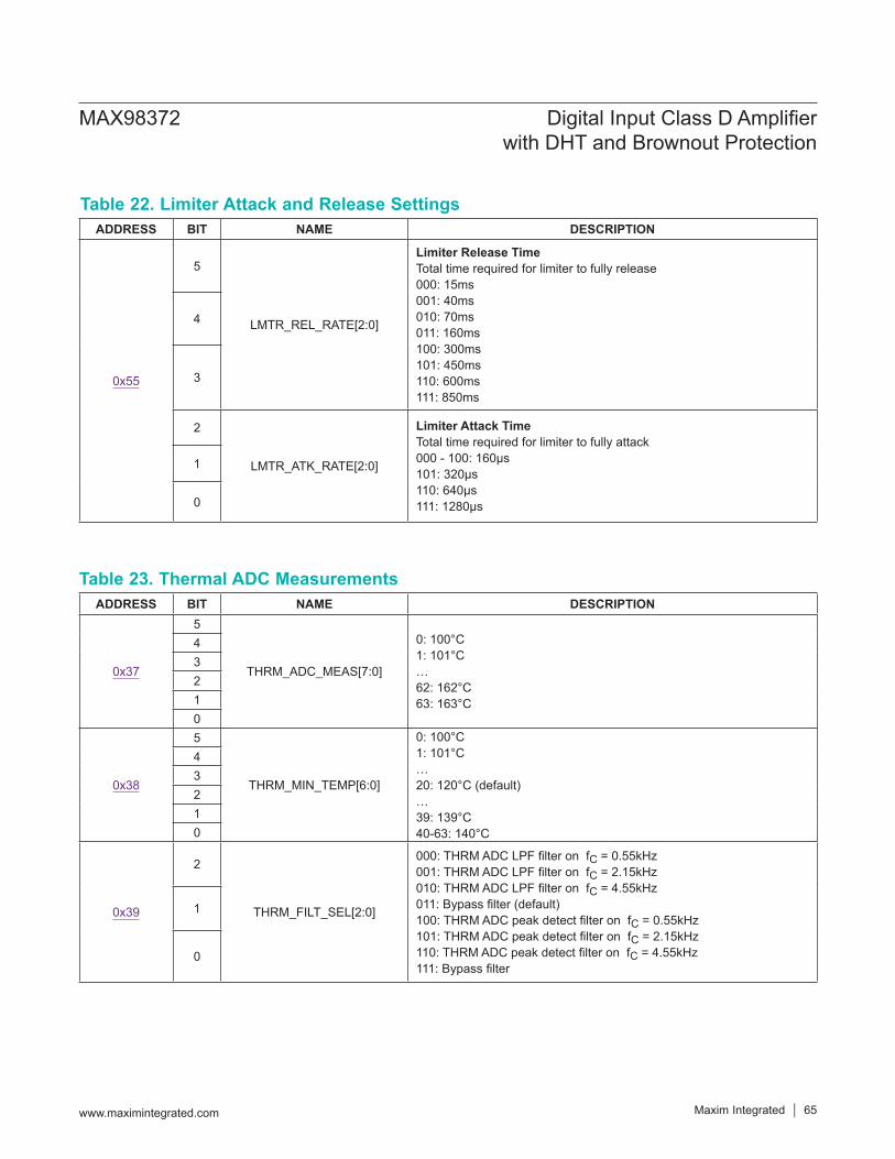
Table 22. Limiter Attack and Release Settings
Table 23. Thermal ADC Measurements
ADDRESS BIT NAME DESCRIPTION
0x55
5
LMTR_REL_RATE[2:0]
Limiter Release TimeTotal time required for limiter to fully release000: 15ms001: 40ms010: 70ms011: 160ms100: 300ms101: 450ms110: 600ms111: 850ms
4
3
2
LMTR_ATK_RATE[2:0]
Limiter Attack TimeTotal time required for limiter to fully attack000 - 100: 160µs101: 320µs110: 640µs111: 1280µs
1
0
ADDRESS BIT NAME DESCRIPTION
0x37
5
THRM_ADC_MEAS[7:0]
0: 100°C1: 101°C…62: 162°C63: 163°C
43210
0x38
5
THRM_MIN_TEMP[6:0]
0: 100°C1: 101°C…20: 120°C (default)…39: 139°C 40-63: 140°C
43210
0x39
2
THRM_FILT_SEL[2:0]
000: THRM ADC LPF filter on fC = 0.55kHz001: THRM ADC LPF filter on fC = 2.15kHz010: THRM ADC LPF filter on fC = 4.55kHz011: Bypass filter (default)100: THRM ADC peak detect filter on fC = 0.55kHz101: THRM ADC peak detect filter on fC = 2.15kHz110: THRM ADC peak detect filter on fC = 4.55kHz111: Bypass filter
1
0
www.maximintegrated.com Maxim Integrated 65
MAX98372 Digital Input Class D Amplifier with DHT and Brownout Protection

The thermal foldback feature can be turned on through the THRM_FB_EN bit, default is off (Table 25). The release rate of the attenuation and the slope of the effect can be set by the user (Table 24), the attack time is fixed at 10µs/dB.THRM_HOLD controls how long the temperature must stay on one side of the hysteresis threshold. THRM_REL controls the release rate of the attenuation applied by the thermal foldback circuit. THRM_SLOPE controls the amount of attenuation per °C. See Table 24.Regardless of whether the thermal foldback feature is enabled, the thermal warning bit in the interrupt registers assert and generate an interrupt through the Interrupt Mask register when thermal foldback threshold tempera-ture is crossed.
Table 24. Thermal Foldback Settings
Table 25. Thermal Foldback Enable
Figure 15. Thermal Foldback Performance
ADDRESS BIT NAME DESCRIPTION
0X36
7THRM_HOLD[1:0]
Thermal Foldback Hold Settings00: 0ms01: 20ms10: 40ms11: 80ms (default)
6
5 0 Unused: Read back is 0.4 0 Unused: Read back is 0.
3THRM_REL[1:0]
Thermal Foldback Release Times00: 3ms/dB01: 10ms/dB10: 100ms/dB11: 300ms/dB
2
1
THRM_SLOPE[1:0]
Thermal Foldback Slope Settings00: 0.5dB/°C01: 1.0dB/°C10: 2.0dB/°C11: Reserved
0
ADDRESS BIT NAME DESCRIPTION
0x4C 0 THRM_FB_ENThermal Foldback Enable0: Thermal foldback disabled1: Thermal foldback enabled
www.maximintegrated.com Maxim Integrated 66
MAX98372 Digital Input Class D Amplifier with DHT and Brownout Protection

Automatic Level Control (ALC)The MAX98372 automatic level control feature (ALC) reduces the amplifier gain at the PGA if the battery volt-age drops below a programmable brownout threshold preventing battery collapse. ALC compares PVDD to the programmable brownout threshold set by ALC_TH and ALC_RANGE. When PVDD drops below the brownout threshold the ALC reduces amplifier gain at a program-mable attack rate and step size set by ALC_ATK_RATE and ALC_ATK_STEP. The gain change occurs immedi-ately even when zero-cross detection is enabled. PGA gain reduction is programmable from 1dB to 9dB in 1dB steps below the nominal setting of the GAIN register (reg-ister 0x64, ALC_MAX_ATTEN). If gain reductions cause the battery voltage to rise above the brownout threshold, the gain reduction stops to a level where PVDD again drops below the brownout threshold after a programmable debounce time set by ALC_RLS_DBT. The rate at which the gain is restored is set by ALC_RLS_RATE and ALC_RLS_CFG. If the battery supply voltage remains below the brownout threshold after the amplifier gain has been reduced by programmed setting, the speaker amplifier is, by default, muted after a programmable delay time set by
ALC_MUTE_DLY. The battery debounce time ALC_RLS_DBT is the time the battery must be above the threshold before moving to the RELEASE state either from the MUTE state or the HOLD state. The transition to MUTE can be disabled by resetting the ALC_MUTE_EN bit. If ALC_RLS_DBT is set to infinite hold, the gain remains either muted or at the programmed reduction level below the nominal PGA gain setting until the ALS_RLS_TGR bit is set. When ALC_MUTE_EN bit is set the gain remains at programmed reduction value below the PGA gain setting until PVDD rises above the brownout threshold. ALC gain reductions are independent of the minimum attenuation setting of the PGA. If enabled, gain ramping has no effect on ALC attack, release or mute actions. Figure 16–Figure 19 provide examples of how the ALC behaves in four scenarios. If PVDD is held close to the ALC threshold, ALC will be stuck in a state of intermedi-ate attenuation. Intermediate Attenuation means that ALC started to reduce gain but never reaches the programmed maximum attenuation. Gain is constant in this state, in-between original gain and maximum attenuation as ALC is neither attacking of releasing. Figure 20 shows an example of ALC Intermediate attenuation.
Figure 16. ALC Example 1: Battery Drops Below Brownout Threshold and Quickly Recovers
VPVDDPROGRAMMABLE
THRESHOLD
SPEAKER GAIN ATTACK RATE PER
ATTACK STEP
RELEASE DE-BOUNCE TIME
RELEASE RATE
VPVDD DROPS BELOW THRESHOLD
14dB
5dB
MUTE
MAX ATTENUATION(0dB to 9dB)
ALCTH
t
t
www.maximintegrated.com Maxim Integrated 67
MAX98372 Digital Input Class D Amplifier with DHT and Brownout Protection

Figure 17. ALC Example 2: Battery Drops Below Brownout Threshold and Stays Low
V PVDD PROGRAMMABLE THRESHOLD
SPEAKER GAIN ATTACK RATE PER
ATTACK STEP
MUTE DELAY
VPVDD DROPS BELOW THRESHOLD
14dB
5dB
MUTE
MAX ATTENUATION(0dB to 9dB)
ALCTH
MUTE ENABLED
t
t
www.maximintegrated.com Maxim Integrated 68
MAX98372 Digital Input Class D Amplifier with DHT and Brownout Protection

Figure 18. ALC Example 3: Battery Drops Below Brownout Threshold and Stays Long Enough for the Amp to Mute (Non-Infinite Hold Time)
VPVDD PROGRAMMABLE THRESHOLD
SPEAKER GAIN ATTACK RATE PER
ATTACK STEP
VPVDD DROPS BELOW THRESHOLD
14dB
5dB
MUTE
MAX ATTENUATION(0dB to 9dB)
ALCTH
MUTE ENABLED, NON-INFINITE HOLD
t
t
RELEASE RATE
RELEASE DE-BOUNCE TIME
www.maximintegrated.com Maxim Integrated 69
MAX98372 Digital Input Class D Amplifier with DHT and Brownout Protection
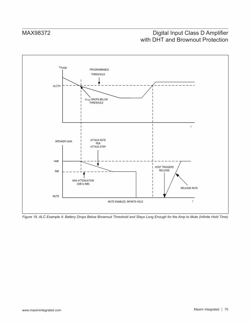
Figure 19. ALC Example 4: Battery Drops Below Brownout Threshold and Stays Long Enough for the Amp to Mute (Infinite Hold Time)
VPVDD PROGRAMMABLE THRESHOLD
SPEAKER GAIN ATTACK RATE PER
ATTACK STEP
VPVDD DROPS BELOW THRESHOLD
14dB
5dB
MUTE
MAX ATTENUATION(0dB to 9dB)
ALCTH
MUTE ENABLED, INFINITE HOLD
t
t
RELEASE RATE
HOST TRIGGERS RELEASE
www.maximintegrated.com Maxim Integrated 70
MAX98372 Digital Input Class D Amplifier with DHT and Brownout Protection
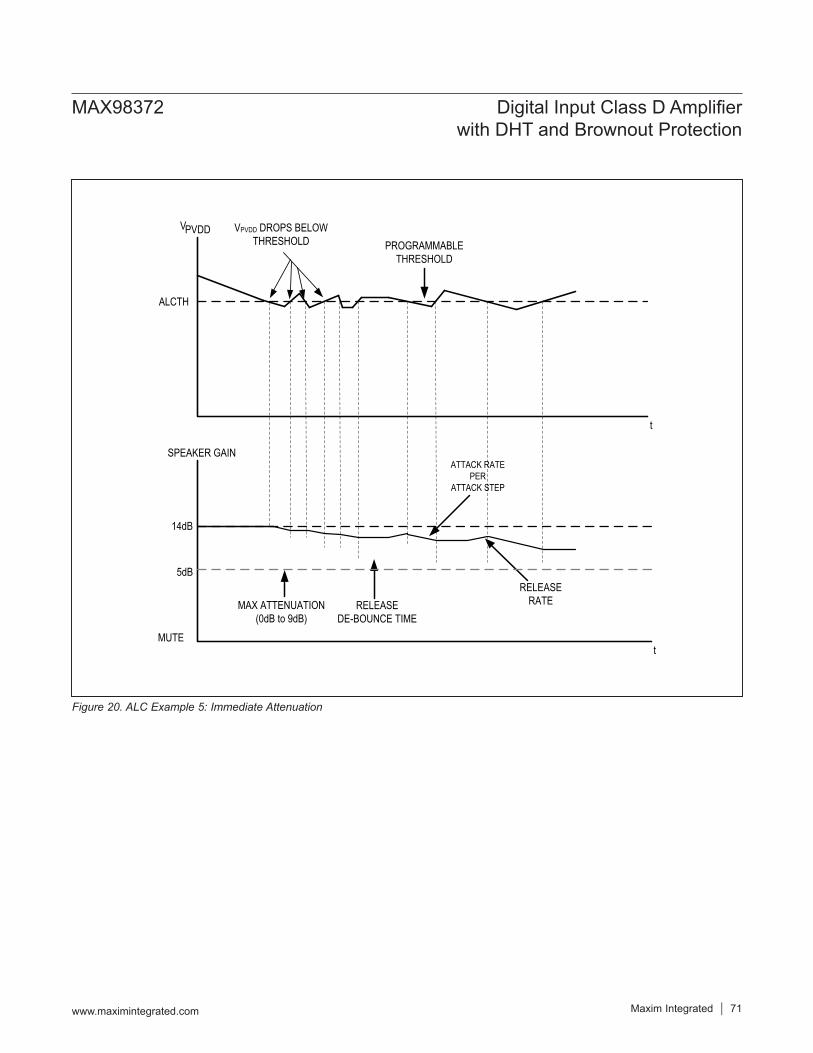
Figure 20. ALC Example 5: Immediate Attenuation
VPVDDPROGRAMMABLE
THRESHOLD
SPEAKER GAINATTACK RATE
PER ATTACK STEP
RELEASE DE-BOUNCE TIME
RELEASE RATE
VPVDD DROPS BELOW THRESHOLD
14dB
5dB
MUTE
MAX ATTENUATION(0dB to 9dB)
ALCTH
t
t
www.maximintegrated.com Maxim Integrated 71
MAX98372 Digital Input Class D Amplifier with DHT and Brownout Protection

Table 26. ALC ThresholdADDRESS BIT NAME DESCRIPTION
0x62
7 0 Unused: Read back is 0.
6 ALC_RANGE 0: 2-cell operation (default)1: 3-cell operation
5 ALC_EN 0: ALC is not enabled (default)1: ALC is enabled.
4
ALC_TH[4:0]
Value (Hex) ALC_RANGE = 0 ALC_RANGE = 100 — 7.8001 — 7.9502 — 8.1003 5.5 8.25
04 5.6 8.40
3
05 5.7 8.5506 5.8 8.70
07 5.9 8.85
08 6.0 9.0009 6.1 9.15
2
0A 6.2 (default) 9.30 (default)0B 6.3 9.450C 6.4 9.600D 6.5 9.75
1
0E 6.6 9.900F 6.7 10.0510 6.8 10.20
11 6.9 10.35
0
12 7.0 10.50
13 7.1 10.65
14 7.2 10.8015 7.3 10.95
www.maximintegrated.com Maxim Integrated 72
MAX98372 Digital Input Class D Amplifier with DHT and Brownout Protection

Table 27. ALC Attack
Table 28. ALC Attenuation and Release
ADDRESS BIT NAME DESCRIPTION
0x63
7
ALC_ATK_STEP[3:0]
ALC Attack step0: -1 dB step (default)1: -2 dB Step2: -3 dB Step3: -4 dB Step4: -5 dB Step5: -6 dB Step6: -7 dB Step7: -8 dB Step8: -9 dB Step…F: -9 dB Step
6
5
4
3 0 Unused: Read back is 0.
2
ATK_RATE
ALC Attack rate000: 10ms/step (default)001: 20ms/step010: 40ms/step011: 80ms/step100: 160ms/step101: 320ms/step110: 640ms/step111: 1280ms/step
1
0
ADDRESS BIT NAME DESCRIPTION
0x64
7
ALC_MAX_ATTEN[3:0]
ALC Maximum Gain Reduction Setting (dB)0000: -10001: -20010: -30011: -40100: -50101: -60110: -70111: -81000: -9 (default)
6
5
4
3 0 Unused: Read back is 0.
2
ATK_RLS_RATE[2:0]
ALC Release rates (ms/dB)000: 10 (default)001: 50010: 100011: 250100: 500101: 750110: 1000111: 1500
1
0
www.maximintegrated.com Maxim Integrated 73
MAX98372 Digital Input Class D Amplifier with DHT and Brownout Protection

Table 29. ALC Infinite Hold Release
Table 30. ALC Configuration
ADDRESS BIT NAME DESCRIPTION
0x65
7ALC_RLS_CFG[1:0]
00: Uses ALC_RLS_RATE[2:0] as defined01: 8x faster release rate10: 64x faster release rate11: 512x faster release rate6
5 0 Unused: Read back is 0.
4 0 Unused: Read back is 0.
3 0 Unused: Read back is 0.
2 0 Unused: Read back is 0.
1 0 Unused: Read back is 0.
0 ALC_RLS_TGR
0: Register is self-clearing and always read back as ‘0’1: If Infinite HOLD is enabled, write a ‘1’ to unlock the release phase. If infinite HOLD is enabled and a ‘1’ is written while a battery low event is occurring, the gain is NOT released
ADDRESS BIT NAME DESCRIPTION
0x66
7 ALC_MUTE_EN 0: ALC cannot mute the channel path1: ALC can mute the channel path (default)
6
ALC_MUTE_DLY[2:0]
Delay Before Onset of Mute000: 0.3ms001: 0.6ms (default)010: 1ms011: 3ms100: 4.5ms101: 6ms110: 15ms111: 30ms
5
4
3 0 Unused: Read back is 0.
2
ALC_RLS_DBT[2:0]
Battery Debounce Time (ms)000: 10001: 100010: 250 (default)011: 500100: 0.01101: 0.1110: 1111: Infinite hold
1
0
www.maximintegrated.com Maxim Integrated 74
MAX98372 Digital Input Class D Amplifier with DHT and Brownout Protection
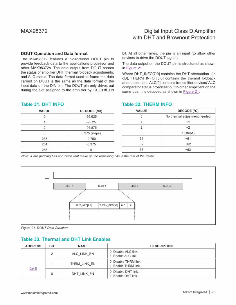
Note: X are padding bits and zeros that make up the remaining bits in the rest of the frame.
DOUT Operation and Data formatThe MAX98372 features a bidirectional DOUT pin to provide feedback data to the applications processor and other MAX98372s. The data output from DOUT shares the status of amplifier DHT, thermal foldback adjustments, and ALC status. The data format used to frame the data carried on DOUT is the same as the data format of the input data on the DIN pin. The DOUT pin only drives out during the slot assigned to the amplifier by TX_CH#_EN
bit. At all other times, the pin is an input (to allow other devices to drive the DOUT signal).The data output on the DOUT pin is structured as shown in Figure 21.Where DHT_INFO[7:0] contains the DHT attenuation (in dB), THERM_INFO [5:0] contains the thermal foldback attenuation, and ALC[0] contains transmitter devices’ ALC comparator status broadcast out to other amplifiers on the same bus. It is decoded as shown in Figure 21.
Table 31. DHT INFO Table 32. THERM INFO
Table 33. Thermal and DHT Link Enables
Figure 21. DOUT Data Structure
DHT_INFO[7:0]
SLOT 1 SLOT 2 SLOT 3 SLOT 4
THERM_INFO[5:0] XALC
VALUE DECODE (dB)0 -95.6251 -95.252 -94.875… 0.375 (steps)
253 -0.750254 -0.375255 0
VALUE DECODE (°C)0 No thermal adjustment needed1 +12 +2… 1 (steps)61 +6162 +6263 +63
ADDRESS BIT NAME DESCRIPTION
2 ALC_LINK_EN 0: Disable ALC link.1: Enable ALC link.
0x4E1 THRM_LINK_EN 0: Disable THRM link.
1: Enable THRM link.
0 DHT_LINK_EN 0: Disable DHT link.1: Enable DHT link.
www.maximintegrated.com Maxim Integrated 75
MAX98372 Digital Input Class D Amplifier with DHT and Brownout Protection
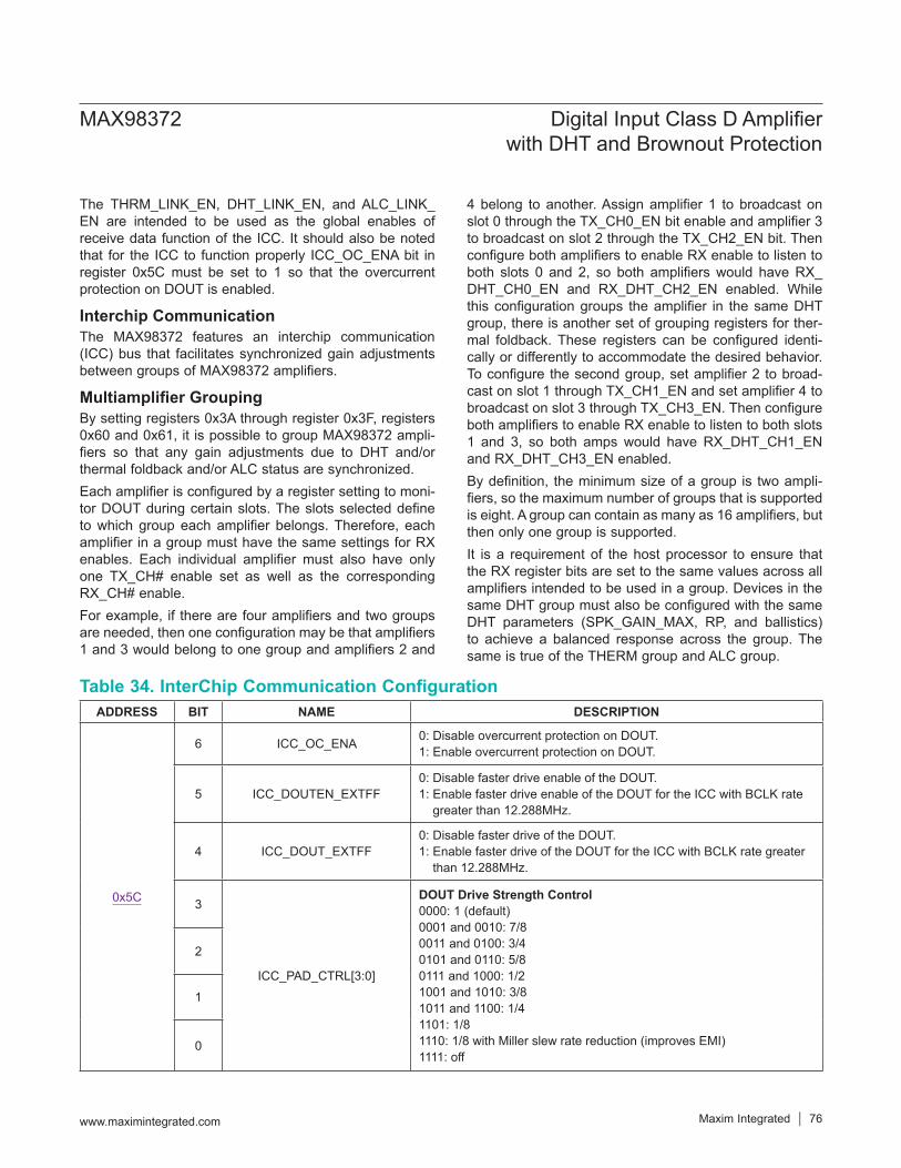
The THRM_LINK_EN, DHT_LINK_EN, and ALC_LINK_EN are intended to be used as the global enables of receive data function of the ICC. It should also be noted that for the ICC to function properly ICC_OC_ENA bit in register 0x5C must be set to 1 so that the overcurrent protection on DOUT is enabled.
Interchip CommunicationThe MAX98372 features an interchip communication (ICC) bus that facilitates synchronized gain adjustments between groups of MAX98372 amplifiers.
Multiamplifier GroupingBy setting registers 0x3A through register 0x3F, registers 0x60 and 0x61, it is possible to group MAX98372 ampli-fiers so that any gain adjustments due to DHT and/or thermal foldback and/or ALC status are synchronized.Each amplifier is configured by a register setting to moni-tor DOUT during certain slots. The slots selected define to which group each amplifier belongs. Therefore, each amplifier in a group must have the same settings for RX enables. Each individual amplifier must also have only one TX_CH# enable set as well as the corresponding RX_CH# enable.For example, if there are four amplifiers and two groups are needed, then one configuration may be that amplifiers 1 and 3 would belong to one group and amplifiers 2 and
4 belong to another. Assign amplifier 1 to broadcast on slot 0 through the TX_CH0_EN bit enable and amplifier 3 to broadcast on slot 2 through the TX_CH2_EN bit. Then configure both amplifiers to enable RX enable to listen to both slots 0 and 2, so both amplifiers would have RX_DHT_CH0_EN and RX_DHT_CH2_EN enabled. While this configuration groups the amplifier in the same DHT group, there is another set of grouping registers for ther-mal foldback. These registers can be configured identi-cally or differently to accommodate the desired behavior. To configure the second group, set amplifier 2 to broad-cast on slot 1 through TX_CH1_EN and set amplifier 4 to broadcast on slot 3 through TX_CH3_EN. Then configure both amplifiers to enable RX enable to listen to both slots 1 and 3, so both amps would have RX_DHT_CH1_EN and RX_DHT_CH3_EN enabled.By definition, the minimum size of a group is two ampli-fiers, so the maximum number of groups that is supported is eight. A group can contain as many as 16 amplifiers, but then only one group is supported.It is a requirement of the host processor to ensure that the RX register bits are set to the same values across all amplifiers intended to be used in a group. Devices in the same DHT group must also be configured with the same DHT parameters (SPK_GAIN_MAX, RP, and ballistics) to achieve a balanced response across the group. The same is true of the THERM group and ALC group.
Table 34. InterChip Communication ConfigurationADDRESS BIT NAME DESCRIPTION
0x5C
6 ICC_OC_ENA 0: Disable overcurrent protection on DOUT. 1: Enable overcurrent protection on DOUT.
5 ICC_DOUTEN_EXTFF0: Disable faster drive enable of the DOUT. 1: Enable faster drive enable of the DOUT for the ICC with BCLK rate greater than 12.288MHz.
4 ICC_DOUT_EXTFF0: Disable faster drive of the DOUT. 1: Enable faster drive of the DOUT for the ICC with BCLK rate greater than 12.288MHz.
3
ICC_PAD_CTRL[3:0]
DOUT Drive Strength Control0000: 1 (default)0001 and 0010: 7/80011 and 0100: 3/40101 and 0110: 5/80111 and 1000: 1/21001 and 1010: 3/81011 and 1100: 1/41101: 1/81110: 1/8 with Miller slew rate reduction (improves EMI)1111: off
2
1
0
www.maximintegrated.com Maxim Integrated 76
MAX98372 Digital Input Class D Amplifier with DHT and Brownout Protection

Double Data DriveIf the shared DOUT trace has a high capacitance that needs to be driven at high speed then the double-data drive feature can be used. This gives a longer drive time for each device.When the BCLK is less than or equal to 25MHz, DOUT can be clocked with standard clocking: data changes on the falling edge and is valid on the rising edge of each BCLK (Table 35).When the BCLK is greater than 25MHz, DOUT should be clocked using a double-data drive method: data changes on the falling edge and is valid on the second rising edge.
In this way, the DOUT data transfer rate is effectively half of the BCLK speed. This is accomplished by setting DRIVE_MODE = 1.This has implications for the supported slot lengths. When double-data drive is enabled, only 32-bit slot lengths are permitted.Additional MAX98372 devices correctly interpret the double-data drive format (if enabled). Any other attached hardware, such as an applications processor, which is expecting standard timing, needs to ensure that it omits away the information captured on the nonvalid rising edge each time and reconstruct the samples accordingly.
Table 35. DOUT Double Data Drive Mode
Figure 22. Single Data Drive
31 30 29 28 27 26 25 24 23 22
DHT [7]
DHT [6]
DHT [5]
DHT [4]
DHT [3]
DHT [2]
DHT [1]
DHT [0]
THM [5]
THM [4]
THM [3]
THM [2]
THM [1]
THM [0]
21 20 19 18 17
DRIVE DATA ONFALLING EDGE
RECEIVE DATA ON RISING EDGE
THREE-STATE DATA AT END OF SLOT
ALC [0]
16
Figure 23. Double Data Drive illustration
31 30 29 28 27 26 25
DHT [7] DHT [6] DHT [5] DHT [4]
24
tDRIVE
ADDRESS BIT NAME DESCRIPTION
0x40 3 DRIVE_MODE 0: Single data drive (default)1: Double data drive
www.maximintegrated.com Maxim Integrated 77
MAX98372 Digital Input Class D Amplifier with DHT and Brownout Protection

Table 36. DOUT DHT Receive Channel ConfigurationADDRESS BIT NAME DESCRIPTION
0x3A
7 RXDHT_CH7_EN 0: DHT receive channel 7 is disabled.1: DHT receive channel 7 is enabled.
6 RXDHT_CH6_EN 0: DHT receive channel 6 is disabled.1: DHT receive channel 6 is enabled.
5 RXDHT_CH5_EN 0: DHT receive channel 5 is disabled.1: DHT receive channel 5 is enabled.
4 RXDHT_CH4_EN 0: DHT receive channel 4 is disabled.1: DHT receive channel 4 is enabled.
3 RXDHT_CH3_EN 0: DHT receive channel 3 is disabled.1: DHT receive channel 3 is enabled.
2 RXDHT_CH2_EN 0: DHT receive channel 2 is disabled.1: DHT receive channel 2 is enabled.
1 RXDHT_CH1_EN 0: DHT receive channel 1 is disabled.1: DHT receive channel 1 is enabled.
0 RXDHT_CH0_EN 0: DHT receive channel 0 is disabled.1: DHT receive channel 0 is enabled.
0x3B
7 RXDHT_CH15_EN 0: DHT receive channel 15 is disabled.1: DHT receive channel 15 is enabled.
6 RXDHT_CH14_EN 0: DHT receive channel 14 is disabled.1: DHT receive channel 14 is enabled.
5 RXDHT_CH13_EN 0: DHT receive channel 13 is disabled.1: DHT receive channel 13 is enabled.
4 RXDHT_CH12_EN 0: DHT receive channel 12 is disabled.1: DHT receive channel 12 is enabled.
3 RXDHT_CH11_EN 0: DHT receive channel 11 is disabled.1: DHT receive channel 11 is enabled.
2 RXDHT_CH10_EN 0: DHT receive channel 10 is disabled.1: DHT receive channel 10 is enabled.
1 RXDHT_CH9_EN 0: DHT receive channel 9 is disabled.1: DHT receive channel 9 is enabled.
0 RXDHT_CH8_EN 0: DHT receive channel 8 is disabled.1: DHT receive channel 8 is enabled.
www.maximintegrated.com Maxim Integrated 78
MAX98372 Digital Input Class D Amplifier with DHT and Brownout Protection

Table 37. DOUT Thermal Foldback Receive Channel ConfigurationADDRESS BIT NAME DESCRIPTION
0x3C
7 RXTHM_CH7_EN 0: THRM FB receive channel 7 is disabled.1: THRM FB receive channel 7 is enabled.
6 RXTHM_CH6_EN 0: THRM FB receive channel 6 is disabled.1: THRM FB receive channel 6 is enabled.
5 RXTHM_CH5_EN 0: THRM FB receive channel 5 is disabled.1: THRM FB receive channel 5 is enabled.
4 RXTHM_CH4_EN 0: THRM FB receive channel 4 is disabled.1: THRM FB receive channel 4 is enabled.
3 RXTHM_CH3_EN 0: THRM FB receive channel 3 is disabled.1: THRM FB receive channel 3 is enabled.
2 RXTHM_CH2_EN 0: THRM FB receive channel 2 is disabled.1: THRM FB receive channel 2 is enabled.
1 RXTHM_CH1_EN 0: THRM FB receive channel 1 is disabled.1: THRM FB receive channel 1 is enabled.
0 RXTHM_CH0_EN 0: THRM FB receive channel 0 is disabled.1: THRM FB receive channel 0 is enabled.
0x3D
7 RXTHM_CH15_EN 0: THRM FB receive channel 15 is disabled.1: THRM FB receive channel 15 is enabled.
6 RXTHM_CH14_EN 0: THRM FB receive channel 14 is disabled.1: THRM FB receive channel 14 is enabled.
5 RXTHM_CH13_EN 0: THRM FB receive channel 13 is disabled.1: THRM FB receive channel 13 is enabled.
4 RXTHM_CH12_EN 0: THRM FB receive channel 12 is disabled.1: THRM FB receive channel 12 is enabled.
3 RXTHM_CH11_EN 0: THRM FB receive channel 11 is disabled.1: THRM FB receive channel 11 is enabled.
2 RXTHM_CH10_EN 0: THRM FB receive channel 10 is disabled.1: THRM FB receive channel 10 is enabled.
1 RXTHM_CH9_EN 0: THRM FB receive channel 9 is disabled.1: THRM FB receive channel 9 is enabled.
0 RXTHM_CH8_EN 0: THRM FB receive channel 8 is disabled.1: THRM FB receive channel 8 is enabled.
www.maximintegrated.com Maxim Integrated 79
MAX98372 Digital Input Class D Amplifier with DHT and Brownout Protection
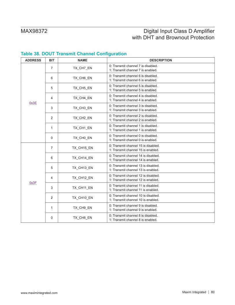
Table 38. DOUT Transmit Channel ConfigurationADDRESS BIT NAME DESCRIPTION
0x3E
7 TX_CH7_EN 0: Transmit channel 7 is disabled.1: Transmit channel 7 is enabled.
6 TX_CH6_EN 0: Transmit channel 6 is disabled.1: Transmit channel 6 is enabled.
5 TX_CH5_EN 0: Transmit channel 5 is disabled.1: Transmit channel 5 is enabled.
4 TX_CH4_EN 0: Transmit channel 4 is disabled.1: Transmit channel 4 is enabled.
3 TX_CH3_EN 0: Transmit channel 3 is disabled.1: Transmit channel 3 is enabled.
2 TX_CH2_EN 0: Transmit channel 2 is disabled.1: Transmit channel 2 is enabled.
1 TX_CH1_EN 0: Transmit channel 1 is disabled.1: Transmit channel 1 is enabled.
0 TX_CH0_EN 0: Transmit channel 0 is disabled.1: Transmit channel 0 is enabled.
0x3F
7 TX_CH15_EN 0: Transmit channel 15 is disabled.1: Transmit channel 15 is enabled.
6 TX_CH14_EN 0: Transmit channel 14 is disabled.1: Transmit channel 14 is enabled.
5 TX_CH13_EN 0: Transmit channel 13 is disabled.1: Transmit channel 13 is enabled.
4 TX_CH12_EN 0: Transmit channel 12 is disabled.1: Transmit channel 12 is enabled.
3 TX_CH11_EN 0: Transmit channel 11 is disabled.1: Transmit channel 11 is enabled.
2 TX_CH10_EN 0: Transmit channel 10 is disabled.1: Transmit channel 10 is enabled.
1 TX_CH9_EN 0: Transmit channel 9 is disabled.1: Transmit channel 9 is enabled.
0 TX_CH8_EN 0: Transmit channel 8 is disabled.1: Transmit channel 8 is enabled.
www.maximintegrated.com Maxim Integrated 80
MAX98372 Digital Input Class D Amplifier with DHT and Brownout Protection

Table 39. DOUT ALC Receive Channel ConfigurationADDRESS BIT NAME DESCRIPTION
0x60
7 RXALC_CH7_EN 0: ALC FB receive channel 7 is disabled.1: ALC FB receive channel 7 is enabled.
6 RXALC_CH6_EN 0: ALC FB receive channel 6 is disabled.1: ALC FB receive channel 6 is enabled.
5 RXALC_CH5_EN 0: ALC FB receive channel 5 is disabled.1: ALC FB receive channel 5 is enabled.
4 RXALC_CH4_EN 0: ALC FB receive channel 4 is disabled.1: ALC FB receive channel 4 is enabled.
3 RXALC_CH3_EN 0: ALC FB receive channel 3 is disabled.1: ALC FB receive channel 3 is enabled.
2 RXALC_CH2_EN 0: ALC FB receive channel 2 is disabled.1: ALC FB receive channel 2 is enabled.
1 RXALC_CH1_EN 0: ALC FB receive channel 1 is disabled.1: ALC FB receive channel 1 is enabled.
0 RXALC_CH0_EN 0: ALC FB receive channel 0 is disabled.1: ALC FB receive channel 0 is enabled.
0x61
7 RXALC_CH15_EN 0: ALC FB receive channel 15 is disabled.1: ALC FB receive channel 15 is enabled.
6 RXALC_CH14_EN 0: ALC FB receive channel 14 is disabled.1: ALC FB receive channel 14 is enabled.
5 RXALC_CH13_EN 0: ALC FB receive channel 13 is disabled.1: ALC FB receive channel 13 is enabled.
4 RXALC_CH12_EN 0: ALC FB receive channel 12 is disabled.1: ALC FB receive channel 12 is enabled.
3 RXALC_CH11_EN 0: ALC FB receive channel 11 is disabled.1: ALC FB receive channel 11 is enabled.
2 RXALC_CH10_EN 0: ALC FB receive channel 10 is disabled.1: ALC FB receive channel 10 is enabled.
1 RXALC_CH9_EN 0: ALC FB receive channel 9 is disabled.1: ALC FB receive channel 9 is enabled.
0 RXALC_CH8_EN 0: ALC FB receive channel 8 is disabled.1: ALC FB receive channel 8 is enabled.
www.maximintegrated.com Maxim Integrated 81
MAX98372 Digital Input Class D Amplifier with DHT and Brownout Protection

Table 40. Extra BCLK Cycle Configuration
Table 41. Manual High-Impedance Mode Configuration
ADDRESS BIT NAME DESCRIPTION
0x41 1 TX_EXTRA_HIZ 0: Extra BCLK cycles are driven to zero.1: Extra BCLK cycles are driven to high impedance.
ADDRESS BIT NAME DESCRIPTION
0X42
7 TX_CH7_HIZ 0: Transmit Channel 7 outputs data/zeros.1: Transmit Channel 7 outputs high impedance.
6 TX_CH6_HIZ 0: Transmit Channel 6 outputs data/zeros.1: Transmit Channel 6 outputs high impedance.
5 TX_CH5_HIZ 0: Transmit Channel 5 outputs data/zeros.1: Transmit Channel 5 outputs high impedance.
4 TX_CH4_HIZ 0: Transmit Channel 4 outputs data/zeros.1: Transmit Channel 4 is enabled.
3 TX_CH3_HIZ 0: Transmit Channel 3 outputs data/zeros.1: Transmit Channel 3 outputs high impedance.
2 TX_CH2_HIZ 0: Transmit Channel 2 outputs data/zeros.1: Transmit Channel 2 outputs high impedance.
1 TX_CH1_HIZ 0: Transmit Channel 1 outputs data/zeros.1: Transmit Channel 1 outputs high impedance.
0 TX_CH0_HIZ 0: Transmit Channel 0 outputs data/zeros.1: Transmit Channel 0 outputs high impedance.
0x43
7 TX_CH15_HIZ 0: Transmit Channel 15 outputs data/zeros.1: Transmit Channel 15 outputs high impedance.
6 TX_CH14_HIZ 0: Transmit Channel 14 outputs data/zeros.1: Transmit Channel 14 outputs high impedance.
5 TX_CH13_HIZ 0: Transmit Channel 13 outputs data/zeros.1: Transmit Channel 13 outputs high impedance.
4 TX_CH12_HIZ 0: Transmit Channel 12 outputs data/zeros.1: Transmit Channel 12 outputs high impedance.
3 TX_CH11_HIZ 0: Transmit Channel 11 outputs data/zeros.1: Transmit Channel 11 outputs high impedance.
2 TX_CH10_HIZ 0: Transmit Channel 10 outputs data/zeros.1: Transmit Channel 10 outputs high impedance.
1 TX_CH9_HIZ 0: Transmit Channel 9 outputs data/zeros.1: Transmit Channel 9 outputs high impedance.
0 TX_CH8_HIZ 0: Transmit Channel 8 outputs data/zeros.1: Transmit Channel 8 outputs high impedance.
www.maximintegrated.com Maxim Integrated 82
MAX98372 Digital Input Class D Amplifier with DHT and Brownout Protection

Class D Output StageThe MAX98372 Class D output stage with active emis-sions limiting and spread spectrum provides optimum suppression and control of output switching harmonics that most directly contribute to EMI and radiated emis-sions. Programmable speaker edge rate control is avail-able to help tweak EMI performance. As the edge rate increases the efficiency goes up slightly, and as the edge
rate slows the efficiency goes down. Set the speaker edge rate with bits SPK_EDGE bits in register 0x4A.The default Class D output switching frequency is 472kHz for the best THD performance. To trade off THD perfor-mance for higher efficiency the output switching frequency can be set to 330kHz by setting SPK_SWCLK to 1.Chnages to the SPK_EN bit should only be made when Global Enable (EN) is set low. See Table 42 for speaker configuration.
Table 42. Speaker ConfigurationADDRESS BIT NAME DESCRIPTION
0x4A
7 SPK_SWCLKClass D output Switching Frequency Select0: Speaker switching frequency is set to 472kHz (default).1: Speaker switching frequency is set to 330kHz.
6 0 Unused: Read back is 0.
5 SPK_SSM[1:0] Speaker Spread Spectrum Modulation Control00: SSM is disabled (default)10: SSM is enabled4
3
SPK_EDGE[1:0]
Programmable Speaker Edge Rate Control00: Nominal edge rate (default)01: +15% faster edge rate10: -40% slower edge rate11: -20% slower edge rate
2
1 0 Unused: Read back is 0.
0 SPK_ENSpeaker Amplifier Enable0: Speaker amplifier is disabled (default).1: Speaker amplifier is enabled
www.maximintegrated.com Maxim Integrated 83
MAX98372 Digital Input Class D Amplifier with DHT and Brownout Protection
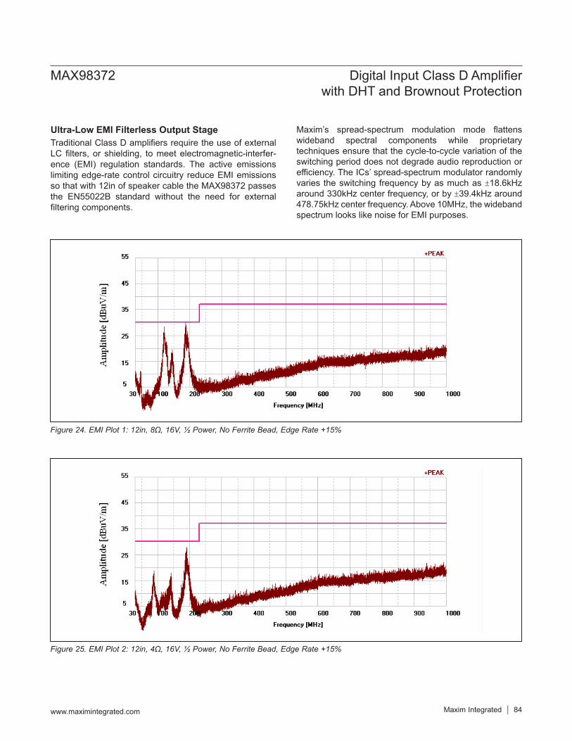
Ultra-Low EMI Filterless Output StageTraditional Class D amplifiers require the use of external LC filters, or shielding, to meet electromagnetic-interfer-ence (EMI) regulation standards. The active emissions limiting edge-rate control circuitry reduce EMI emissions so that with 12in of speaker cable the MAX98372 passes the EN55022B standard without the need for external filtering components.
Maxim’s spread-spectrum modulation mode flattens wideband spectral components while proprietary techniques ensure that the cycle-to-cycle variation of the switching period does not degrade audio reproduction or efficiency. The ICs’ spread-spectrum modulator randomly varies the switching frequency by as much as ±18.6kHz around 330kHz center frequency, or by ±39.4kHz around 478.75kHz center frequency. Above 10MHz, the wideband spectrum looks like noise for EMI purposes.
Figure 24. EMI Plot 1: 12in, 8Ω, 16V, ½ Power, No Ferrite Bead, Edge Rate +15%
Figure 25. EMI Plot 2: 12in, 4Ω, 16V, ½ Power, No Ferrite Bead, Edge Rate +15%
www.maximintegrated.com Maxim Integrated 84
MAX98372 Digital Input Class D Amplifier with DHT and Brownout Protection

Figure 26. EMI Plot 3: 12in, 8Ω, 16V, ½ Power, Ferrite Bead
Figure 27. EMI Plot 4: 12in, 4Ω, 16V, ½ Power, Ferrite Bead
www.maximintegrated.com Maxim Integrated 85
MAX98372 Digital Input Class D Amplifier with DHT and Brownout Protection

VDVDD and VPVDD UVLOThe MAX98372 monitors both DVDD and PVDD for low voltage conditions that would prevent the speaker amplifier from operating normally. If the voltage on DVDD drops below the DVDD-UVLO threshold (VDVDD-UVLO), the device is placed in hardware shutdown. All the I2C internal registers reset to their default values. The device can be commanded to leave this state through the I2C command if the voltage on DVDD later exceeds the VDVDD-UVLO threshold.If the voltage PVDD drops below the PVDD-UVLO thresh-old, the audio output is muted to prevent the PVDD supply from being used by the amplifier. If the voltage on PVDD later exceeds the VPVDD-UVLO threshold, the device can be commanded to unmute through the I2C command.
Click-and-Pop SuppressionThe MAX98372 speaker amplifier features Maxim’s com-prehensive click-and-pop suppression. During power-up and power-down, the click-and-pop suppression circuitry reduces any audible transient sources internal to the device.At startup, the PGA gain is automatically ramped from mute to the desired setting at a rate of 200µs/dB. Similarly, the gain is ramped down to mute at shutdown at the same rate. For faster startup and shutdown, disable gain ramping.
During normal operation, any requested gain changes are ramped from the old value to the new value at a value determined by the ballistics within the volume control block.
Amplifier Current LimitThe MAX98372 features current limit protection that pro-tects the device against shorts. If the output current of the speaker amplifier exceeds the current limit (6A typ) the IC disables the outputs for approximately 100µs. After 100ms, the outputs are reenabled. If the fault condition still exists, the IC continues to disable and reenable the outputs until the fault condition is removed. Set OVC_SEL low to disable this behavior (Table 44). The current limit protects against both high-current and short-circuit events.
Thermal Shutdown RecoveryWhen the temperate of the die exceeds +150°C, the part enters thermal shutdown. However, the MAX98372 features a configurable thermal shutdown autorecov-ery mode. When the die temperate has decreased by 30°C from the thermal shutdown event, the MAX98372 attempts to resume the previous operating state. Set TSHDN_AUTO_RESTART high to enable autorecovery mode (Table 44).
Table 43. Spread-Spectrum Modulation ConfigurationADDRESS BIT NAME DESCRIPTION
0x49
7 0 Unused: Read back is 0.
6 0 Unused: Read back is 0.
5 0 Unused: Read back is 0.
4 0 Unused: Read back is 0.
3 0 Unused: Read back is 0.
2
SSM_MODINDEX
Spread Spectrum Modulation Index SelectionSSM_MODINDEX Modulation
0x0 ±7.7% & ±3.8%0x1 (Default) ±6.4% & ±3.8%
10x2 ±5.1% & ±2.6%0x3 ±3.8% & ±2.6%
00x4 ±2.6% & ±1.3%0x5 ±1.3% & ±1.3%
www.maximintegrated.com Maxim Integrated 86
MAX98372 Digital Input Class D Amplifier with DHT and Brownout Protection
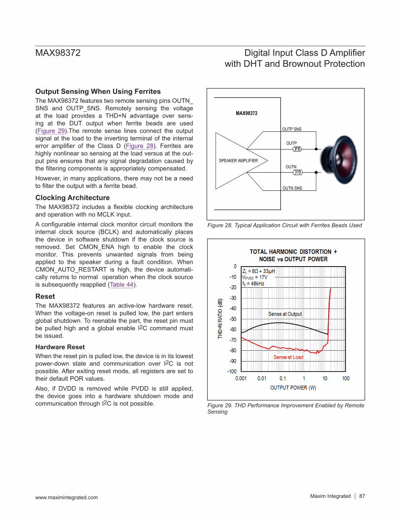
Output Sensing When Using FerritesThe MAX98372 features two remote sensing pins OUTN_SNS and OUTP_SNS. Remotely sensing the voltage at the load provides a THD+N advantage over sens-ing at the DUT output when ferrite beads are used (Figure 29).The remote sense lines connect the output signal at the load to the inverting terminal of the internal error amplifier of the Class D (Figure 28). Ferrites are highly nonlinear so sensing at the load versus at the out-put pins ensures that any signal degradation caused by the filtering components is appropriately compensated.However, in many applications, there may not be a need to filter the output with a ferrite bead.
Clocking ArchitectureThe MAX98372 includes a flexible clocking architecture and operation with no MCLK input.A configurable internal clock monitor circuit monitors the internal clock source (BCLK) and automatically places the device in software shutdown if the clock source is removed. Set CMON_ENA high to enable the clock monitor. This prevents unwanted signals from being applied to the speaker during a fault condition. When CMON_AUTO_RESTART is high, the device automati-cally returns to normal operation when the clock source is subsequently reapplied (Table 44).
ResetThe MAX98372 features an active-low hardware reset. When the voltage-on reset is pulled low, the part enters global shutdown. To reenable the part, the reset pin must be pulled high and a global enable I2C command must be issued.
Hardware ResetWhen the reset pin is pulled low, the device is in its lowest power-down state and communication over I2C is not possible. After exiting reset mode, all registers are set to their default POR values.Also, if DVDD is removed while PVDD is still applied, the device goes into a hardware shutdown mode and communication through I2C is not possible.
Figure 28. Typical Application Circuit with Ferrites Beads Used
MAX98372
OUTP
OUTN
OUTP SNS
OUTN SNS
FB
FB
SPEAKER AMPLIFIER
Figure 29. THD Performance Improvement Enabled by Remote Sensing
www.maximintegrated.com Maxim Integrated 87
MAX98372 Digital Input Class D Amplifier with DHT and Brownout Protection
Table 44. Clock Monitor Configuration
Table 45. Reset Register
Table 46. Global Enable RegisterADDRESS BIT NAME DESCRIPTION
0x50 0 ENGlobal Enable:0: Disabled1: Enabled
ADDRESS BIT NAME DESCRIPTION
0x4D
3 CMON_AUTO_RESTART 0: Device does not restart after a clock monitor event (default).1: Device restarts automatically when BCLK is restarted.
2 CMON_ENA 0: Clock monitor is disabled (default).1: Clock monitor is enabled.
1 OVC_SEL 0: Current limit recovery is in manual mode (default).1: Current limit recovery is in autorecovery mode.
0 TSDHN_AUTO_RESTART 0: Thermal-protection recovery is in manual mode (default).1: Thermal-protection recovery is in autorecovery mode.
ADDRESS BIT NAME DESCRIPTION
0x51 0 RSTReset0: No action is taken.1: Reset. All registers return to their POR (default) values.
www.maximintegrated.com Maxim Integrated 88
MAX98372 Digital Input Class D Amplifier with DHT and Brownout Protection

Software ResetWrite 1 to bit 0 of register 0x51 to trigger a software reset. Software reset is used to return most registers to their default (POR) states. Biquad equalizer coefficients are not reset.The software reset register is a write only register. As a result, a read of this register always returns 0x00. Writing logic-high to RST triggers a software register reset, while writing a logic-low to RST has no effect.Also if PVDD is removed while DVDD is still applied the device goes into software shutdown mode where all blocks are disabled except I2C control block.
I2C Serial InterfaceThe MAX98372 features an I2C 2-wire serial interface consisting of a serial data line (SDA) and a serial clock line (SCL). SDA and SCL facilitate communication between the IC and the master at clock rates up to 400kHz. Figure 30 shows the 2-wire interface timing diagram. The master generates SCL and initiates data transfer on the bus. The master device writes data to the IC by transmitting the proper slave address followed by the register address and then the data word. Each transmit sequence is framed by a START (S) or REPEATED START (Sr) condition and a STOP (P) condition. Each word transmitted to the IC is 8 bits long and is followed by an acknowledge clock pulse. A master reading data from the IC transmits the proper slave address followed by a series of nine SCL pulses. The IC transmits data on SDA in sync with the master-
generated SCL pulses. The master acknowledges receipt of each byte of data. Each read sequence is framed by a START (S) or REPEATED START (Sr) condition, a not acknowledge, and a STOP (P) condition. SDA oper-ates as both an input and an open-drain output. A pullup resistor, typically greater than 500Ω, is required on SDA. SCL operates only as an input. A pullup resistor, typically greater than 500Ω, is required on SCL if there are mul-tiple masters on the bus, or if the single master has an open-drain SCL output. Series resistors in line with SDA and SCL are optional. Series resistors protect the digital inputs of the IC from high voltage spikes on the bus lines, and minimize crosstalk and undershoot of the bus signals.
Bit TransferOne data bit is transferred during each SCL cycle. The data on SDA must remain stable during the high period of the SCL pulse. Changes in SDA while SCL is high are con-trol signals. See the START and STOP Conditions section.
START and STOP ConditionsSDA and SCL idle high when the bus is not in use. A mas-ter initiates communication by issuing a START condition. A START condition is a high-to-low transition on SDA with CL high. A STOP condition is a low-to-high transition on SDA while SCL is high (Figure 30). A START condition from the master signals the beginning of a transmission to the IC. The master terminates transmission, and frees the bus, by issuing a STOP condition. The bus remains active if a REPEATED START condition is generated instead of a STOP condition.
Figure 30. START, STOP, and REPEATED START Conditions
www.maximintegrated.com Maxim Integrated 89
MAX98372 Digital Input Class D Amplifier with DHT and Brownout Protection

Early Stop ConditionsThe IC recognizes a STOP condition at any point during data transmission except if the STOP condition occurs in the same high pulse as a START condition. For proper operation, do not send a STOP condition during the same SCL high pulse as the START condition.
Slave AddressThe slave address is defined as the seven most signifi-cant bits (MSBs) followed by the read/write bit. For the IC, the seven most significant bits are programmable through the ADDR1 and ADDR0 bumps. Setting the read/write bit to 1 configures the IC for read mode. Setting the read/write bit to 0 configures the IC for write mode. The slave
address is the first byte of information sent to the IC after the START condition.
AcknowledgeThe acknowledge bit (ACK) is a clocked 9th bit that the IC uses to handshake receipt each byte of data when in write mode Figure 31. The IC pulls down SDA during the entire master-generated 9th clock pulse if the previous byte is successfully received. Monitoring ACK allows for detection of unsuccessful data transfers. An unsuccessful data transfer occurs if a receiving device is busy or if a system fault has occurred. In the event of an unsuccessful data transfer, the bus master reattempts communication. The master pulls down SDA during the 9th clock cycle to acknowledge receipt of data when the IC is in read mode. An acknowledge is sent by the master after each read byte to allow data transfer to continue. A not-acknowledge is sent when the master reads the final byte of data from the IC, followed by a STOP condition.
Write Data FormatA write to the IC includes transmission of a START con-dition, the slave address with the R/W bit set to 0, one byte of data to configure the internal register address pointer, one or more bytes of data, and a STOP condition. Figure 32 illustrates the proper frame format for writing one byte of data to the IC. Figure 33 illustrates the frame format for writing n-bytes of data to the IC.Figure 31. Acknowledge
Figure 32. Writing One Byte of Data to the MAX98372
A0SLAVE ADDRESS REGISTER ADDRESS DATA BYTE
ACKNOWLEDGE FROM SLAVE
R/W 1 BYTE
AUTOINCREMENT INTERNALREGISTER ADDRESS POINTER
ACKNOWLEDGE FROM SLAVE
ACKNOWLEDGE FROM SLAVE
B1 B0B3 B2B5 B4B7 B6
S AA P
Figure 33. n-Bytes of Data to the MAX98372
1 BYTE
AUTOINCREMENT INTERNAL REGISTER ADDRESS POINTER
ACKNOWLEDGEFROM SLAVE
ACKNOWLEDGEFROM SLAVE
B1 B0B3 B2B5 B4B7 B6
A A0
ACKNOWLEDGE FROM SLAVE
R/W
S A
1 BYTE
ACKNOWLEDGEFROM SLAVE
B1 B0B3 B2B5 B4B7 B6
PASLAVE ADDRESS REGISTER ADDRESS DATA BYTE 1 DATA BYTE n
www.maximintegrated.com Maxim Integrated 90
MAX98372 Digital Input Class D Amplifier with DHT and Brownout Protection

The slave address with the R/W bit set to 0 indicates that the master intends to write data to the IC. The IC acknowledges receipt of the address byte during the master-generated 9th SCL pulse.The second byte transmitted from the master configures the IC’s internal register address pointer. The pointer tells the IC where to write the next byte of data. An acknowl-edge pulse is sent by the IC upon receipt of the address pointer data.The third byte sent to the IC contains the data that is writ-ten to the chosen register. An acknowledge pulse from the IC signals receipt of the data byte. The address pointer autoincrements to the next register address after each received data byte. This autoincrement feature allows a master to write to sequential registers within one continu-ous frame. The master signals the end of transmission by issuing a STOP condition.
Read Data FormatSend the slave address with the R/W bit set to 1 to initiate a read operation. The IC acknowledges receipt of its slave address by pulling SDA low during the 9th SCL clock pulse. A START command followed by a read command resets the address pointer to register 0x00.
The first byte transmitted from the IC is the content of register 0x00. Transmitted data is valid on the rising edge of SCL. The address pointer autoincrements after each read data byte. This autoincrement feature allows all registers to be read sequentially within one continuous frame. A STOP condition can be issued after any number of read data bytes. If a STOP condition is issued followed by another read operation, the first data byte to be read is from register 0x00.The address pointer can be preset to a specific register before a read command is issued. The master presets the address pointer by first sending the IC’s slave address with the R/W bit set to 0 followed by the register address. A REPEATED START condition is then sent followed by the slave address with the R/W bit set to 1. The IC then trans-mits the contents of the specified register. The address pointer autoincrements after transmitting the first byte.The master acknowledges receipt of each read byte during the acknowledge clock pulse. The master must acknowl-edge all correctly received bytes except the last byte. The final byte must be followed by a not acknowledge from the master and then a STOP condition. Figure 34 illustrates the frame format for reading one byte from the IC. Figure 35 illustrates the frame format for reading multiple bytes from the IC.
Figure 34. Reading One Byte of Data from the MAX98372
ACKNOWLEDGE FROM SLAVE
1 BYTE
AUTOINCREMENT INTERNALREGISTER ADDRESS POINTER
ACKNOWLEDGE FROM SLAVE
AA A0
ACKNOWLEDGE FROM SLAVE
R/W
S
R/WREPEATED START
Sr 1SLAVE ADDRESS REGISTER ADDRESS SLAVE ADDRESS DATA BYTE P
Figure 35. Reading n-Bytes of Data from the MAX98372
ACKNOWLEDGE FROM SLAVE
1 BYTE
AUTOINCREMENT INTERNAL REGISTER ADDRESS POINTER
ACKNOWLEDGE FROM SLAVE
AA A0
ACKNOWLEDGE FROM SLAVE
R/W
S
R/WREPEATED
START
Sr 1SLAVE ADDRESS REGISTER ADDRESS SLAVE ADDRESS DATA BYTE P
www.maximintegrated.com Maxim Integrated 91
MAX98372 Digital Input Class D Amplifier with DHT and Brownout Protection

I2C Slave AddressesThe MAX98372 is configured using the I2C control bus. The addresses effectively allow unique audio endpoint des-tinations in systems that use multiples of the device. The IC uses hardware select slave addresses determined by the configuration of ADDR0, ADDR1 as shown in Table 47. See the I2C Serial Interface section for a complete interface description.
Applications InformationLayout and GroundingProper layout and grounding are essential for optimum performance. Use at least 4 PCB layers, and add thermal vias to the ground/power plane close to the MAX98372 to ensure good thermal performance and high-end out-put power. Good grounding improves audio performance and prevents switching noise from coupling into the audio signal. Ground the power signals and the analog signals of the IC separately at the system ground plane, to prevent switching interference from corrupting sensi-tive analog signals.Place the recommended supply decoupling capacitors as close as possible to the IC. The PVDD-to-PGND connection must be kept short and should have minimum trace length and loop area to ensure optimumal performance.
Use wide, low-resistance output, supply and ground traces. As load impedance decreases, the current drawn from the device outputs increase. At higher current, the resistance of the output traces decreases the power delivered to the load. For example, if 2W is delivered from the speaker output to a 4Ω load through a 100mΩ trace, 49mW is consumed in the trace. If power is deliv-ered through a 10mΩ trace, only 5mW is consumed in the trace. Wide output, supply, and ground traces also improve the power dissipation of the device.The MAX98372 is inherently designed for excellent RF immunity. For best performance, add ground fills around all signal traces on the top and bottom PCB planes.It is generally advisable to follow the layout of the MAX98372 evaluation kit as closely as is practical in the application.Thermal and performance measurements shown in this data sheet were measured with a 6-layer board with 2 signal layers and 4 ground layers. As a result, the EV kit performance is likely better than what can be achieved with a JEDEC standard board.
Table 47. ADDR I2C Address SelectADDR1 ADDR0 I2C WRITE ADDRESS SELECT
ADDR1 connected to DVDD ADDR0 connected to DGND 0x62ADDR1 connected to DGND ADDR0 connected to DGND 0x64ADDR1 connected to SDA ADDR0 connected to DGND 0x66ADDR1 connected to SCL ADDR0 connected to DGND 0x68
ADDR1 connected to DVDD ADDR0 connected to SDA 0x6AADDR1 connected to DGND ADDR0 connected to SDA 0x6CADDR1 connected to SDA ADDR0 connected to SDA 0x6EADDR1 connected to SCL ADDR0 connected to SDA 0x70
ADDR1 connected to DVDD ADDR0 connected to DVDD 0x72ADDR1 connected to DGND ADDR0 connected to DVDD 0x74ADDR1 connected to SDA ADDR0 connected to DVDD 0x76ADDR1 connected to SCL ADDR0 connected to DVDD 0x78
ADDR1 connected to DVDD ADDR0 connected to SCL 0x7AADDR1 connected to DGND ADDR0 connected to SCL 0x7CADDR1 connected to SDA ADDR0 connected to SCL 0x7EADDR1 connected to SCL ADDR0 connected to SCL 0x80
www.maximintegrated.com Maxim Integrated 92
MAX98372 Digital Input Class D Amplifier with DHT and Brownout Protection
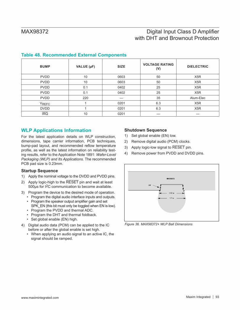
WLP Applications InformationFor the latest application details on WLP construction, dimensions, tape carrier information, PCB techniques, bump-pad layout, and recommended reflow temperature profile, as well as the latest information on reliability test-ing results, refer to the Application Note 1891: Wafer-Level Packaging (WLP) and Its Applications. The recommended PCB pad size is 0.23mm.
Startup Sequence1) Apply the nominal voltage to the DVDD and PVDD pins.2) Apply logic-high to the RESET pin and wait at least
500µs for I2C communication to become available.3) Program the device to the desired mode of operation.
• Program the digital audio interface inputs and outputs.• Program the speaker output amplifier gain and set
SPK_EN (this bit must only be toggled when EN is low).• Program the PVDD and thermal ADC.• Program the DHT and thermal foldback.• Set global enable (EN) high.
4) Digital audio data (PCM) can be applied to the IC before or after the global enable is set high.
• When applying an audio signal to an active IC, the signal should be ramped.
Shutdown Sequence1) Set global enable (EN) low.2) Remove digital audio (PCM) clocks.3) Apply logic-low signal to RESET pin.4) Remove power from PVDD and DVDD pins.
Table 48. Recommended External Components
Figure 36. MAX98372+ WLP Ball Dimensions
BUMP VALUE (µF) SIZE VOLTAGE RATING (V) DIELECTRIC
PVDD 10 0603 50 X5RPVDD 10 0603 50 X5RPVDD 0.1 0402 25 X5RPVDD 0.1 0402 25 X5RPVDD 220 — 35 Alum-ElecVREFC 1 0201 6.3 X5RDVDD 1 0201 6.3 X5RIRQ 10 0201 — —
www.maximintegrated.com Maxim Integrated 93
MAX98372 Digital Input Class D Amplifier with DHT and Brownout Protection
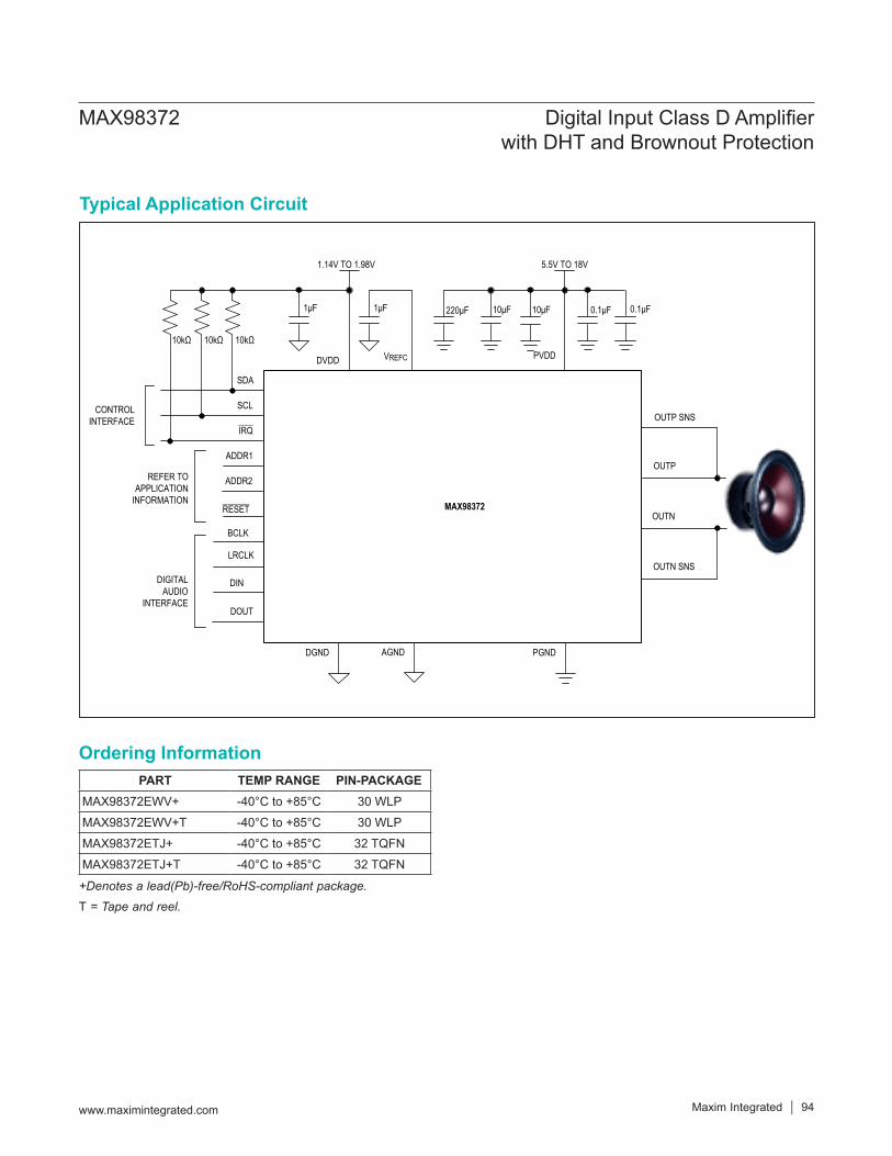
+Denotes a lead(Pb)-free/RoHS-compliant package.
T = Tape and reel.
Typical Application Circuit
MAX98372
SCL
IRQ
DVDD PVDD10kΩ
1μF 1μF
1.14V TO 1.98V
220μF 10μF 0.1μF
5.5V TO 18V
CONTROL INTERFACE
SDA
ADDR1
VREFC
RESET
BCLK
LRCLK
DINDIGITAL AUDIO
INTERFACE
DGND PGNDAGND
OUTP
OUTN
OUTP SNS
OUTN SNS
REFER TO APPLICATION
INFORMATION
ADDR2
10μF 0.1μF
DOUT
10kΩ10kΩ
PART TEMP RANGE PIN-PACKAGEMAX98372EWV+ -40°C to +85°C 30 WLPMAX98372EWV+T -40°C to +85°C 30 WLPMAX98372ETJ+ -40°C to +85°C 32 TQFNMAX98372ETJ+T -40°C to +85°C 32 TQFN
www.maximintegrated.com Maxim Integrated 94
MAX98372 Digital Input Class D Amplifier with DHT and Brownout Protection
Ordering Information
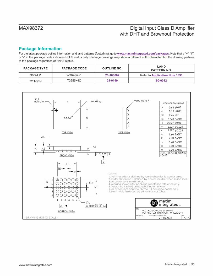
PACKAGE TYPE PACKAGE CODE OUTLINE NO. LAND PATTERN NO.
30 WLP W302G2+1 21-100002 Refer to Application Note 1891
32 TQFN T3255+4C 21-0140 90-0012
www.maximintegrated.com Maxim Integrated 95
MAX98372 Digital Input Class D Amplifier with DHT and Brownout Protection
Package InformationFor the latest package outline information and land patterns (footprints), go to www.maximintegrated.com/packages. Note that a “+”, “#”, or “-” in the package code indicates RoHS status only. Package drawings may show a different suffix character, but the drawing pertains to the package regardless of RoHS status.
e
E1
D1
b
SE
SD
0.05 M S AB
B
A
E
D
Pin 1Indicator Marking see Note 7
A3
A2 A A1
0.05 S
S
FRONT VIEW
TOP VIEW
BOTTOM VIEW
A
10.640.190.45
0.0400.27
1.602.000.400.000.20
A
AAAA
SIDE VIEW
2.2072.797
1 65432
EDCB
TITLE
DOCUMENT CONTROL NO. REV. 11
APPROVAL
COMMON DIMENSIONS
A
A2
A1
A3
b
E1
D1
e
SD
SE
0.050.03
0.03BASICREF
BASIC
NOTES:1. Terminal pitch is defined by terminal center to center value.2. Outer dimension is defined by center lines between scribe lines.3. All dimensions in millimeter.4. Marking shown is for package orientation reference only.5. Tolerance is ± 0.02 unless specified otherwise.6. All dimensions apply to PbFree (+) package codes only.7. Front - side finish can be either Black or Clear.
BASICBASIC
- DRAWING NOT TO SCALE - A
BASICBASIC
maxim integrated TM
21-100002
PACKAGE OUTLINE 30 BUMPSWLP PKG. 0.4 mm PITCH, W302G2+1
D 0.0250.025E
DEPOPULATED BUMPS:NONE
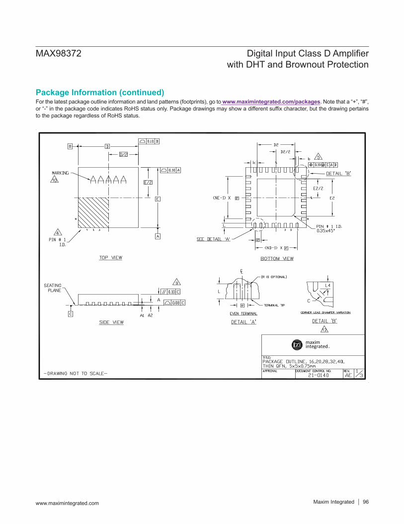
www.maximintegrated.com Maxim Integrated 96
MAX98372 Digital Input Class D Amplifier with DHT and Brownout Protection
Package Information (continued)For the latest package outline information and land patterns (footprints), go to www.maximintegrated.com/packages. Note that a “+”, “#”, or “-” in the package code indicates RoHS status only. Package drawings may show a different suffix character, but the drawing pertains to the package regardless of RoHS status.
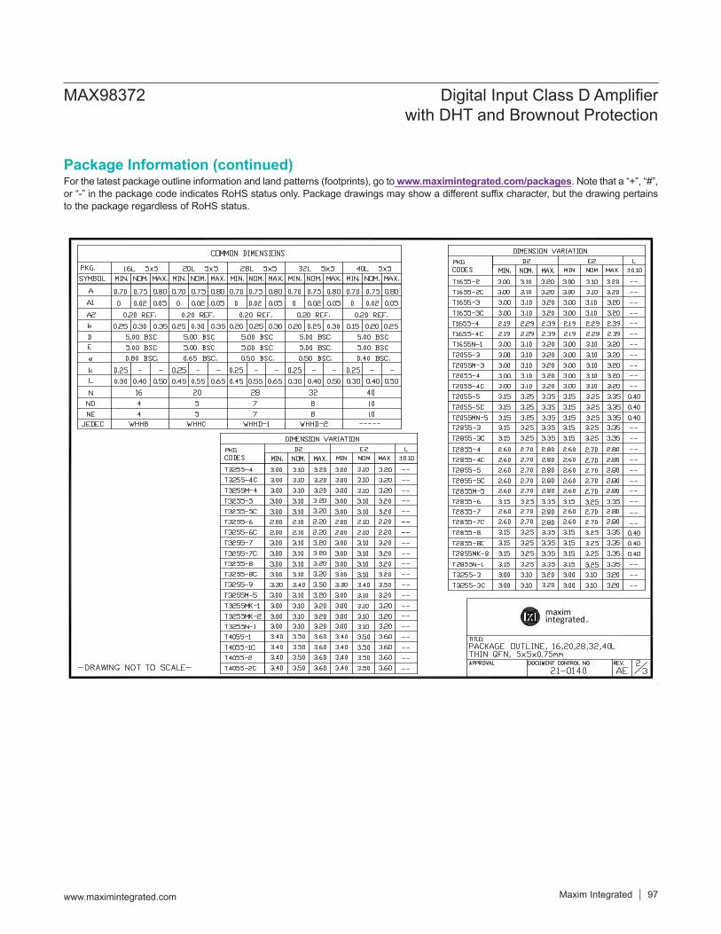
www.maximintegrated.com Maxim Integrated 97
MAX98372 Digital Input Class D Amplifier with DHT and Brownout Protection
Package Information (continued)For the latest package outline information and land patterns (footprints), go to www.maximintegrated.com/packages. Note that a “+”, “#”, or “-” in the package code indicates RoHS status only. Package drawings may show a different suffix character, but the drawing pertains to the package regardless of RoHS status.
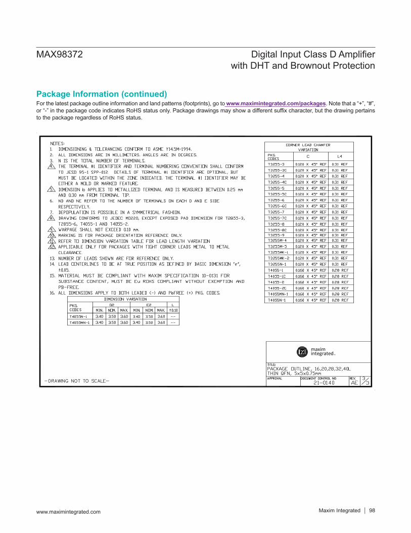
www.maximintegrated.com Maxim Integrated 98
MAX98372 Digital Input Class D Amplifier with DHT and Brownout Protection
Package Information (continued)For the latest package outline information and land patterns (footprints), go to www.maximintegrated.com/packages. Note that a “+”, “#”, or “-” in the package code indicates RoHS status only. Package drawings may show a different suffix character, but the drawing pertains to the package regardless of RoHS status.
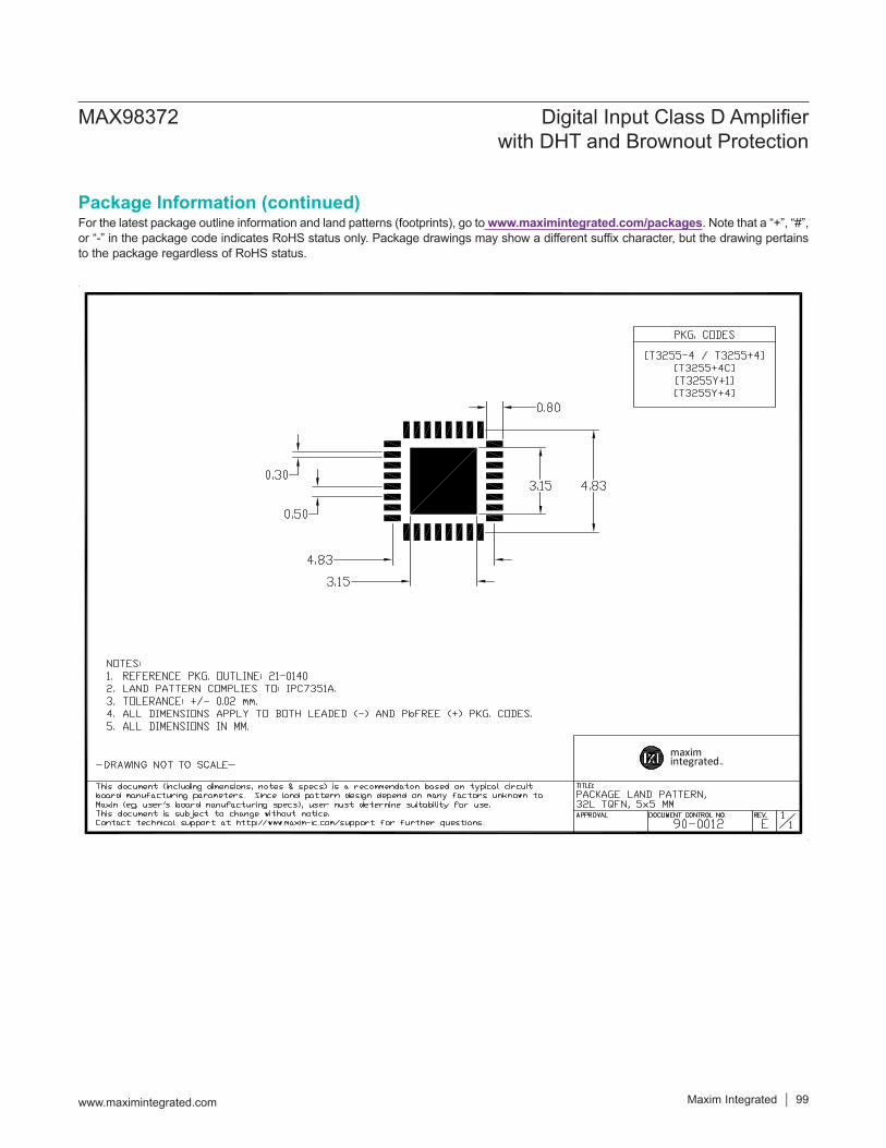
www.maximintegrated.com Maxim Integrated 99
MAX98372 Digital Input Class D Amplifier with DHT and Brownout Protection
Package Information (continued)For the latest package outline information and land patterns (footprints), go to www.maximintegrated.com/packages. Note that a “+”, “#”, or “-” in the package code indicates RoHS status only. Package drawings may show a different suffix character, but the drawing pertains to the package regardless of RoHS status.

Revision HistoryREVISIONNUMBER
REVISIONDATE DESCRIPTION PAGES
CHANGED0 9/15 Initial release —
1 1/16 Updated Electrical Characteristics table DIN Frame Delay after LRCLK Edge parameter, replaced Figure 7 12, 48
2 2/17
Added TQFN package information to Absolute Maximum Ratings and Package Information sections (including package outline drawings), updated Tables 1, 36, 9, 24, 2630, 33, 4244, added four new figures (Figure 24Figure 27), added Startup Sequence and Shutdown Sequence sections, added MAX98372ETJ+ and MAX98372ETJ+T in Ordering Information table
8, 29, 4345, 51, 66, 7275, 8386, 88,
9399
3 8/17 Updated Electrical Characteristics table with current limit specs for different packages 11
Maxim Integrated cannot assume responsibility for use of any circuitry other than circuitry entirely embodied in a Maxim Integrated product. No circuit patent licenses are implied. Maxim Integrated reserves the right to change the circuitry and specifications without notice at any time. The parametric values (min and max limits) shown in the Electrical Characteristics table are guaranteed. Other parametric values quoted in this data sheet are provided for guidance.
Maxim Integrated and the Maxim Integrated logo are trademarks of Maxim Integrated Products, Inc. © 2017 Maxim Integrated Products, Inc. 100
MAX98372 Digital Input Class D Amplifier with DHT and Brownout Protection
For pricing, delivery, and ordering information, please contact Maxim Direct at 1-888-629-4642, or visit Maxim Integrated’s website at www.maximintegrated.com.