max5970 evaluation kit - maxim integrated · tems with two supply voltages between 0 and 16v. ......
TRANSCRIPT
_______________________________________________________________ Maxim Integrated Products 1
For pricing, delivery, and ordering information, please contact Maxim Direct at 1-888-629-4642, or visit Maxim’s website at www.maxim-ic.com.
MAX5970 Evaluation Kit
Eva
lua
tes: M
AX
59
70
19-5220; Rev 0; 4/10
General DescriptionThe MAX5970 evaluation kit (EV kit) is an assembled and tested PCB used to evaluate the MAX5970 dual hot-swap controller, which provides protection for sys-tems with two supply voltages between 0 and 16V. The on-board microcontroller, which is connected to the PC through the universal serial bus (USB) port, acts as the I²C master.
The EV kit also includes WindowsM 2000-, Windows XPM-, and Windows VistaM-compatible software that provides a simple user interface for exercising the MAX5970 features. The program is menu-driven and offers a graphical user interface (GUI) complete with control buttons and status displays. The EV kit comes with the MAX5970ETX+ installed.
FeaturesS Safely Hot Swaps Two Independent 0 to 16V
Power Supplies After Power-Up
S Windows 2000-, Windows XP-, and Windows Vista (32-Bit)-Compatible Software
S On-Board Microcontroller to Generate I2C Commands
S Easy-to-Use, Menu-Driven Software
S USB-PC Connection (Cable Included)
Ordering Information
+Denotes lead(Pb)-free and RoHS compliant.
Component List
Windows, Windows XP, and Windows Vista are registered trademarks of Microsoft Corp.
PART TYPE
MAX5970EVKIT+ EV Kit
DESIGNATION QTY DESCRIPTION
C1, C3–C10, C17, C32
110.1FF Q10%, 16V X7R ceramic capacitors (0603)TDK C1608X7R1C104K
C2, C13, C15, 310FF Q20%, 6.3V X5R ceramic capacitors (0805)TDK C2012X5R0J106M
C11, C12 210pF Q5%, 50V C0G ceramic capacitors (0603)TDK C1608C0G1H100J
C14, C16, C31, C33,
C345
1FF Q10%, 25V X5R ceramic capacitors (0603)Murata GRM188R61E105K
C18, C19 222pF Q5%, 50V C0G ceramic capacitors (0603)TDK C1608C0G1H220J
C20 10.033FF Q10%, 25V X5R ceramic capacitor (0603)Murata GRM188R71E333K
C22, C24, C26, C28
410FF Q10%, 25V X5R ceramic capacitors (1206)Murata GRM31CR61E106K
C21, C30, C25, C29
0Not installed, electrolytic capacitors (12.5mm x 13.5mm)
DESIGNATION QTY DESCRIPTION
C23, C27 24700pF Q10%, 50V X7R ceramic capacitors (0603)TDK C1608X7R1H472K
D1, D6–D9, D14, D15
7 Green LEDs (0603)
D2, D3 2200mA, 25V Schottky diodes (3 SOT23)Fairchild BAT54
D4 1200mA, 30V Schottky diode (3 SOT23)Fairchild BAT54C
D5, D12, D13 3 Red LEDs (0603)
D10, D11 24.7V zener diodes (SOD523)Diodes Inc. BZT52C4V7T
D16, D17 21A, 20V Schottky diodes (SMA)Central Semi CMSH1-20M
GND (x4), VO1, VO2, VS1, VS2
8Noninsulated banana-jack connectors
JU1–JU12 12 3-pin headers
JU13–JU16 4 2-pin headers
MAX5970 Evaluation Kit
Eva
lua
tes:
M
AX
59
70
2 ______________________________________________________________________________________
Note: Indicate that you are using the MAX5970 when contacting these component suppliers.
Component Suppliers
*EP = Exposed pad.
Component List (continued)
SUPPLIER PHONE WEBSITE
Central Semiconductor Corp. 631-435-1110 www.centralsemi.com
Diodes Incorporated 805-446-4800 www.diodes.com
Fairchild Semiconductor 888-522-5372 www.fairchildsemi.com
Hong Kong X’tals Ltd. 852-35112388 www.hongkongcrystal.com
International Rectifier 310-322-3331 www.irf.com
IRC, Inc. 361-992-7900 www.irctt.com
Murata Electronics North America, Inc. 770-436-1300 www.murata-northamerica.com
TDK Corp. 847-803-6100 www.component.tdk.com
DESIGNATION QTY DESCRIPTION
N1, N3 2
30V, 16A n-channel MOSFETs (8 PQFN)International Rectifier IRFH7936PbF
N2, N4 260V, 115mA n-channel MOSFETs (3 SOT23)Diodes Inc. 2N7002-7-F
P1, P2, P3 3-50V, 130mA p-channel MOSFETs (3 SOT23)Diodes Inc. BSS84
R1, R8, R11, R18, R19,
R210
Not installed, resistors (0603) R1, R8, R11, R18 are short (PCB trace); R19, R21 are open
R2 1 220I Q5% resistor (0603)
R3, R26, R30, R31, R38–R46, R48, R49
15 10kI Q5% resistors (0603)
R4 1 2.2kI Q5% resistor (0603)
R5 1 1.5kI Q5% resistor (0603)
R6, R7 2 27I Q5% resistors (0603)
R9, R10 2 4.7kI Q5% resistors (0603)
R12, R13 2 1kI Q1% resistors (0603)
R14, R15, R23, R25,
R27, R29, R327 100kI Q5% resistors (0603)
R16, R17 20.005I Q1%, 2W sense resistors (2512)IRC LRC-LRF-2512LF-01-R005-F
DESIGNATION QTY DESCRIPTION
R20, R22 2 100kI Q1% resistors (0603)
R24, R28, R33–R36
6 1kI Q5% resistors (0603)
R37, R47 2 10I Q5% resistors (0603)
TP1–TP17 17 Test points, red
USB 1USB type-B, right-angle PC-mount receptacle
U1 1Dual, hot-swap controller (36 TQFN-EP*)Maxim MAX5970ETX+
U2 1Microcontroller (68 QFN-EP*)Maxim MAXQ2000-RAX+
U3 1 93C46 type 3-wire EEPROM (8 SO)
U4 1 UART-to-USB converter (32 TQFP)
U5 13.3V regulator (5 SOT23)Maxim MAX8888EZK33+
U6 12.5V regulator (5 SC70)Maxim MAX8511EXK25+
Y1 116MHz crystalHong Kong X’tals SSM16000N1HK188F0-0
Y2 16MHz crystalHong Kong X’tals SSL60000N1HK188F0-0
— 1 USB high-speed A-to-B cables, 6ft
— 16 Shunts
— 1 PCB: MAX5970 EVALUATION KIT+

MAX5970 Evaluation Kit
Eva
lua
tes: M
AX
59
70
_______________________________________________________________________________________ 3
Quick StartRequired Equipment
• MAX5970 EV kit (USB cable included)
• User-supplied Windows 2000, Windows XP, or Windows Vista PC with a spare USB port
• Two 3.3V to 16V DC power supplies
• Two voltmeters
Note: In the following sections, software-related items are identified by bolding. Text in bold refers to items directly from the EV kit software. Text in bold and under-lined refers to items from the Windows operating system.
ProcedureThe MAX5970 EV kit is fully assembled and test-ed. Follow the steps below to verify board operation. Caution: Do not turn on power supplies until all con-nections are completed.
1) Visit www.maxim-ic.com/evkitsoftware to down-load the latest version of the EV kit software, 5970Rxx.ZIP. Save the EV kit software to a tempo-rary folder and uncompress the ZIP file.
2) Install the EV kit software on your computer by run-ning the INSTALL.EXE program inside the tempo-rary folder. The program files are copied and icons are created in the Windows Start | Programs menu.
3) Verify that all jumpers (JU1–JU16) are in their default positions, as shown in Tables 1 and 3.
4) Set the first DC power supply to 5V and connect to the VS1 and the GND banana-jack connectors on the EV kit board.
5) Set the second DC power supply to 5V and connect to the VS2 and the GND banana-jack connectors on the EV kit board.
6) Connect the first voltmeter to the VO1 and the GND pads on the EV kit board.
7) Connect the second voltmeter to the VO2 and the GND pads on the EV kit board.
8) Connect the USB cable from the PC to the EV kit board. A New Hardware Found window pops up when installing the USB driver for the first time. If a window is not seen that is similar to the one described above after 30s, remove the USB cable from the board and reconnect it. Administrator privi-leges are required to install the USB device driver on Windows.
9) Follow the directions of the Found New Hardware window to install the USB device driver. Manually specify the location of the device driver to be C:\Program Files\MAX5970 (default installation directory) using the Browse button. During device driver installation, Windows may show a warning message indicating that the device driver Maxim uses does not contain a digital signature. This is not an error condition and it is safe to proceed with installation. Refer to the USB_Driver_Help.PDF document included with the software for additional information.
10) Turn on the power supplies.
11) Start the EV kit software by opening its icon in the Start | Programs menu. The EV kit software main window appears, as shown in Figure 1. Observe as the program automatically detects the address of the MAX5970 and starts the main program.
12) Verify that PG1 and PG2 LEDs (D14, D15) are on.
13) Verify that both voltmeters read approximately 5V.
MAX5970 EV Kit Files
FILE DESCRIPTION
INSTALL.EXEInstalls the EV kit files on your computer
MAX5970.EXE Application program
FTD2XX.INF USB driver file
UNINST.INI Uninstalls the EV kit software
USB_Driver_Help.PDF USB driver installation help file

MAX5970 Evaluation Kit
Eva
lua
tes:
M
AX
59
70
4 ______________________________________________________________________________________
Table 1. Jumper Description (JU1–JU16)JUMPER SHUNT POSITION DESCRIPTION
JU1
1-2* Powers the MAX5970 using the VS1, VS2 or VIN input supply
2-3 Powers the MAX5970 using the USB or VIN input supply
Open Powers the MAX5970 using the VIN input supply
JU2 — See Table 3 for SMBus/I²C address settings
JU3 — See Table 3 for SMBus/I²C address settings
JU41-2*
Connects the POL pin of the MAX5970 to DREG through a pullup resistor for active-high PG_ outputs
2-3 Connects the POL pin of the MAX5970 to GND for active-low PG_ outputs
JU5
1-2*Connects the MODE pin of the MAX5970 to DREG through a pullup resistor for the channels to operate as a group
2-3Connects the MODE pin of the MAX5970 to GND for the channels to operate as an individual hot-swap controller
Open The MODE pin of the MAX5970 is not connected and the channels operate as a group
JU6
1-2*Connects the PROT pin of the MAX5970 to DREG through a pullup resistor, allowing ALERT output to be asserted and respective PG_ output deasserted upon critical UV/OV fault
2-3 Connects the PROT pin of the MAX5970 to GND, allowing ALERT output to beasserted, and shuts down respective channel upon critical UV/OV fault
Open The PROT pin of the MAX5970 is not connected and ALERT output asserted uponcritical UV/OV fault
JU71-2* Configures the LED1 pin of the MAX5970 to drive an LED
2-3 Configures the LED1 pin of the MAX5970 as a GPIO
JU81-2* Configures the LED2 pin of the MAX5970 to drive an LED
2-3 Configures the LED2 pin of the MAX5970 as a GPIO
JU91-2* Configures the LED3 pin of the MAX5970 to drive an LED
2-3 Configures the LED3 pin of the MAX5970 as a GPIO
JU101-2* Configures the LED4 pin of the MAX5970 to drive an LED
2-3 Configures the LED4 pin of the MAX5970 as a GPIO
JU11
1-2*Connects the IRNG2 pin of the MAX5970 to DREG, which sets the channel 2 DAC current-sense range to 50mV**
2-3Connects the IRNG2 pin of the MAX5970 to GND, which sets the channel 2 DAC current-sense range to 25mV**
OpenThe IRNG2 pin of the MAX5970 is not connected, which sets the channel 2 DAC current-sense range to 100mV**
JU12
1-2*Connects the IRNG1 pin of the MAX5970 to DREG, which sets the channel 1 DAC current-sense range to 50mV**
2-3Connects the IRNG1 pin of the MAX5970 to GND, which sets the channel 1 DAC current-sense range to 25mV**
OpenThe IRNG1 pin of the MAX5970 is not connected, which sets the channel 1 DAC current-sense range to 100mV**
MAX5970 Evaluation Kit
Eva
lua
tes: M
AX
59
70
_______________________________________________________________________________________ 5
Detailed Description of SoftwareThe MAX5970 EV kit user interface (Figure 1) is easy to operate; use the mouse, or press the Tab key to navigate with the arrow keys. Each of the buttons correspond to bits in the command and configuration bytes. By click-ing on them, the correct I²C-compatible write opera-tion is generated to update the internal registers of the MAX5970.
InterfaceUse the Device Address combo box to select the MAX5970 I²C address. Checking the Silence I2C Activity checkbox stops activity between the microcon-troller and the MAX5970 when the software is idle; other-wise, the software continuously reads the device's status and data registers to check that the device is working properly. These functions create activity on the I²C bus. Use the Read All Registers button to perform a read of all of the MAX5970 registers and update the GUI with each register’s data. The status bar located at the bottom of the GUI displays the status of the registers accessed, and the data received or sent.
ConfigurationThe EV kit software Configuration tab sheet (Figure 1) displays the Grouping (MODE), Fault Management (RETRY), Critical Fault Protection (PROT), and Polarity (POL) general settings at the top, while group-ing channel-specific settings below. See Table 2 for GUI control details for each channel. Check the Deglitch checkboxes located to the right of the OV Critical, OV Warning, UV Warning, UV Critical, and OC Warning input controls to enable the deglitch feature for those settings.
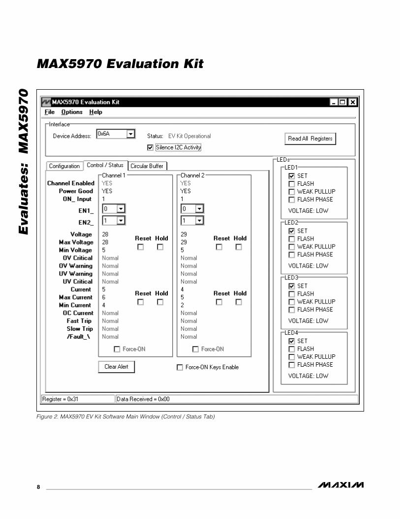
Control and StatusThe EV kit software Control / Status tab sheet (Figure 2) displays the status of each channel, including the volt-age and current measurements in decimal format. Each channel can be enabled, regardless of the input voltage, by configuring the software’s EN1_ and EN2_ combo boxes, or checking the Force-ON Keys Enable and Force-ON checkboxes. Check the corresponding Reset or Hold checkbox to reset or hold the maximum and minimum voltage measurements and the maximum and minimum current measurements. Press the Clear Alert button to clear the alert bit and output signal.
*Default position.**Refer to the MAX5970 IC data sheet for adjusting the circuit breaker threshold range.
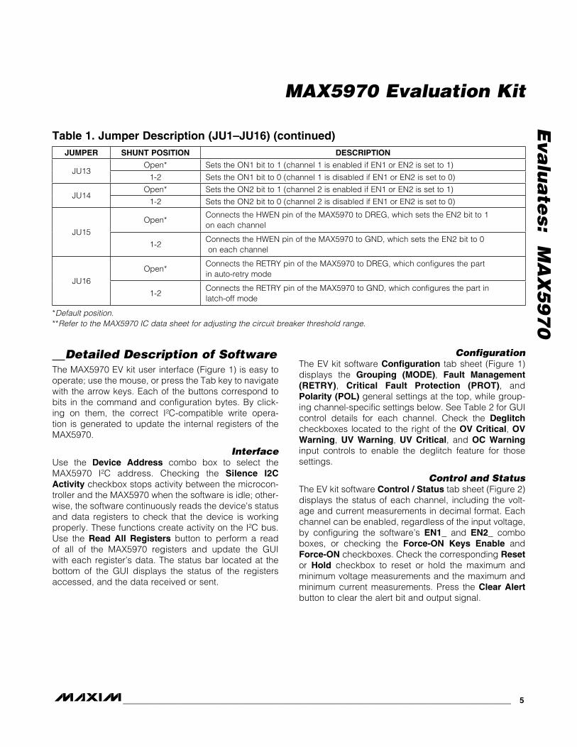
Table 1. Jumper Description (JU1–JU16) (continued)JUMPER SHUNT POSITION DESCRIPTION
JU13Open* Sets the ON1 bit to 1 (channel 1 is enabled if EN1 or EN2 is set to 1)
1-2 Sets the ON1 bit to 0 (channel 1 is disabled if EN1 or EN2 is set to 0)
JU14Open* Sets the ON2 bit to 1 (channel 2 is enabled if EN1 or EN2 is set to 1)
1-2 Sets the ON2 bit to 0 (channel 2 is disabled if EN1 or EN2 is set to 0)
JU15
Open*Connects the HWEN pin of the MAX5970 to DREG, which sets the EN2 bit to 1 on each channel
1-2Connects the HWEN pin of the MAX5970 to GND, which sets the EN2 bit to 0 on each channel
JU16
Open*Connects the RETRY pin of the MAX5970 to DREG, which configures the part in auto-retry mode
1-2Connects the RETRY pin of the MAX5970 to GND, which configures the part in latch-off mode

MAX5970 Evaluation Kit
Eva
lua
tes:
M
AX
59
70
6 ______________________________________________________________________________________
Table 2. Software GUI ControlsGUI CONTROL FUNCTION
Voltage-Sense Range Sets the maximum output voltage range to 2V, 4V, 8V, or 16V.
OV Critical Sets the overvoltage critical limit. Enter a decimal value between 0 and 1023 (10-bit binary value).
OV Warning Sets the overvoltage warning limit. Enter a decimal value between 0 and 1023 (10-bit binary value).
UV Warning Sets the undervoltage warning limit. Enter a decimal value between 0 and 1023 (10-bit binary value).
UV Critical Sets the undervoltage critical limit. Enter a decimal value between 0 and 1023 (10-bit binary value).
Max Current-Sense Sets the maximum current-sense range to 25mV, 50mV, or 100mV across the current-sense resistor.
Fast-trip ThresholdSets the fast-trip voltage threshold across the current-sense resistor between 40% and 100% of the Max Current-Sense setting. Enter a decimal value between 102 and 255 (8-bit binary value).
Fast/Slow Trip Ratio Sets the fast-to-slow trip voltage ratio to 125%, 150%, 175%, or 200% across the current-sense resistor.
OC Warning Sets the overcurrent warning limit. Enter a decimal value between 0 and 1023 (10-bit binary value).
PG Assertion Delay Sets PG_ output signal assertion time delay to 50ms, 100ms, 200ms, or 400ms.
DeglitchEnables deglitching function (two consecutive faults must be detected before the corresponding fault is asserted).
EN1_ Sets EN1 bit 0 or 1.
EN2_ Sets EN2 bit 0 or 1.
Reset Resets the maximum and minimum voltage or current-detection registers of the corresponding channel.
Hold Locks the maximum and minimum voltage or current-detection registers of the corresponding channel.
Force-ON Keys Enable Enables the Force-ON control register.
Force-ON Enables the channel regardless of the input voltage.
Clear Alert Clears the ALERT bit/deasserts the Alert output.
Stop-Delay BufferSets the number of samples that are recorded to a buffer after a shutdown event. Enter a number between 0 and 50.
Voltage Buffer Enables the voltage buffer.
V Read Mode, 8-Bit Sets the circular-buffer resolution to 8 bits.
V Read Mode, 10-Bit Sets the circular-buffer resolution to 10 bits.
Current Buffer Enables the current buffer.
C Read Mode, 8-Bit Sets the circular-buffer resolution to 8 bits.
C Read Mode, 10-Bit Sets the circular-buffer resolution to 10 bits.
Read Voltage Buffer Reads and displays the voltage-buffer data.
Read Current Buffer Reads and displays the current-buffer data.
SET Enables the LED driver pins.
FLASH Enables the flash on the LED driver pins.
WEAK PULLUP Enables the weak pullup on the LED driver pins.
FLASH PHASE Enables the flash to go out of phase on the LED driver pins.

MAX5970 Evaluation Kit
Eva
lua
tes: M
AX
59
70
_______________________________________________________________________________________ 7
Figure 1. MAX5970 EV Kit Software Main Window (Configuration Tab)
MAX5970 Evaluation Kit
Eva
lua
tes:
M
AX
59
70
8 ______________________________________________________________________________________
Figure 2. MAX5970 EV Kit Software Main Window (Control / Status Tab)

MAX5970 Evaluation Kit
Eva
lua
tes: M
AX
59
70
_______________________________________________________________________________________ 9
Circular BufferThe EV kit software Circular Buffer tab sheet (Figure 3) allows the user to control and configure the voltage and current circular buffers for each channel. Each circular buffer always contains a record of the 50 most-recent digital measurements. The resolution of these measure-ments can be set to 8-Bit or 10-Bit. This measurement record includes the number of post-shutdown event
measurements set by the Stop-Delay Buffer setting, if the corresponding buffer (Voltage Buffer or Current Buffer) is set to Run. The corresponding circular buf-fer stops recording new data if it is set to Stop. The 50 measurements contained in the particular buffer are read and displayed when the Read Voltage Buffer or Read Current Buffer buttons are pressed.
Figure 3. MAX5970 EV Kit Software Main Window (Circular Buffer Tab)
MAX5970 Evaluation Kit
Eva
lua
tes:
M
AX
59
70
10 _____________________________________________________________________________________
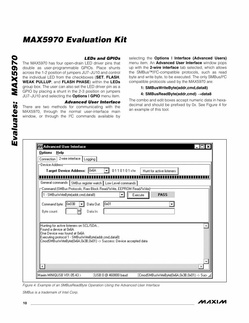
LEDs and GPIOsThe MAX5970 has four open-drain LED driver pins that double as user-programmable GPIOs. Place shunts across the 1-2 position of jumpers JU7–JU10 and control the individual LED from the checkboxes (SET, FLASH, WEAK PULLUP, and FLASH PHASE) within the LEDs group box. The user can also set the LED driver pin as a GPIO by placing a shunt in the 2-3 position on jumpers JU7–JU10 and selecting the Options | GPIO menu item.
Advanced User InterfaceThere are two methods for communicating with the MAX5970, through the normal user-interface main window, or through the I²C commands available by
selecting the Options | Interface (Advanced Users) menu item. An Advanced User Interface window pops up with the 2-wire interface tab selected, which allows the SMBusK/I²C-compatible protocols, such as read byte and write byte, to be executed. The only SMBus/I²C compatible protocols used by the MAX5970 are:
1: SMBusWriteByte(addr,cmd,data8)
4: SMBusReadByte(addr,cmd) →data8
The combo and edit boxes accept numeric data in hexa-decimal and should be prefixed by 0x. See Figure 4 for an example of this tool.
Figure 4. Example of an SMBusReadByte Operation Using the Advanced User Interface
SMBus is a trademark of Intel Corp.
MAX5970 Evaluation Kit
Eva
lua
tes: M
AX
59
70
______________________________________________________________________________________ 11
Detailed Description of HardwareThe MAX5970 EV kit circuit demonstrates the MAX5970 dual-channel hot-swap controller that continually moni-tors the output current and voltage with an internal 10-bit ADC. The MAX5970 controls each channel’s n-channel MOSFET, while monitoring the respective current across the sense resistor and the output voltage. The EV kit requires 3V (2.7V + Schottky diode drop) to 16V DC for normal operation. Each hot-swap channel is configured to operate with an input voltage as low as 0V.
During a startup cycle, the EV kit’s two channels are off until the MAX5970’s IN pin voltage exceeds 2.7V (typ). Once the MAX5970 powers up, it loads the initial operational settings to the internal registers. If any of the input channel’s voltage is above the 0.6V undervoltage threshold, the respective MOSFET is turned on and the MAX5970 controller monitors the corresponding channel output current and voltage.
The EV kit features several jumpers to program the ini-tial operational settings. These settings are maximum current-sense range for each channel, fault-protection behavior, power-good output-signal polarity, hardware enable, fault-management mode, and I²C address for the controller.
Input Power SourcesThe EV kit requires a 3.3V (2.7V + Schottky diode drop) to 16V input DC source for normal EV kit operation. The EV kit circuit features jumper JU1 that allows the user to select one of three methods to provide power to the MAX5970 IC (U1). If the shunt is connected across pins 1-2 on jumper JU1, the highest voltage source connect-ed to the VS1, VS2, or VIN inputs supplies power to the IC. If the shunt is connected across pins 2-3, the highest voltage between the 3.3V source (derived from the USB 5V supply) and the VIN input supplies power to the IC. If the shunt is removed, the VIN input supplies power to U1. Connect a 3.3V to 16V power source across the VIN and GND pads when using this option. See Table 1 for jumper JU1 configuration.
Address SelectionThe MAX5970’s slave I²C address is configured through the A0 and A1 pins. The EV kit features jumpers JU2 and JU3 to configure these pins. The default address is 0110 101 (R/W). See Table 3 for a complete list of addresses. Verify that the new I²C address matches the address shown in the software’s Device Address combo box.
*Default position.
Table 3. Shunt Setting for SMBus/I²C AddressSHUNT POSITION
B7 B6 B5 B4 B3 B2 B1 B0WRITE
ADDRESS(hex)
READ ADDRESS
(hex)JU3(A1)
JU2(A0)
Open Open 0 1 1 0 0 0 0 R/W 0x60 0x61
Open 1-2 0 1 1 0 0 0 1 R/W 0x62 0x63
Open 2-3 0 1 1 0 0 1 0 R/W 0x64 0x65
1-2 Open 0 1 1 0 1 0 0 R/W 0x68 0x69
1-2* 1-2* 0 1 1 0 1 0 1 R/W 0x6A 0x6B
1-2 2-3 0 1 1 0 1 1 0 R/W 0x6C 0x6D
2-3 Open 0 1 1 1 0 1 1 R/W 0x70 0x71
2-3 1-2 0 1 1 1 0 0 1 R/W 0x72 0x73
2-3 2-3 0 1 1 1 0 1 0 R/W 0x74 0x75
MAX5970 Evaluation Kit
Eva
lua
tes:
M
AX
59
70
12 _____________________________________________________________________________________
Hot-Swap Channel EnableDuring startup, each hot-swap channel is enabled if the respective EN2 bit is set to 1 and the ON_ input is high. The EN2 bit is dependent on the state of the HWEN pin. If the HWEN pin is pulled to DREG during startup, the EN2 bit for both channels is set to 1. The EV kit circuit provides jumper JU15 to configure the HWEN pin. See Table 1 for jumper JU15 configuration. Connecting the HWEN pin to GND after startup does not change the EN2 bit state to 0. However, after startup, the EN2 bit state for each channel can be changed using the EV kit GUI software.
Whenever the ON_ pin voltage exceeds the input-voltage threshold of 0.6V (typ), the ON_ bit is set to 1; otherwise, it is set to 0. The EV kit circuit is configured to pull up the ON_ pins to the respective VS_ channel inputs through resistors R20 or R22. The VS_ input undervoltage thresh-old can be modified by completing the resistive divider at each ON_ pin. Use the following equation to select the value for each ON_ resistor:
UVLO
100kR
VS_1
0.6V
Ω= −
where VS_UVLO is the desired VS1 or VS2 undervoltage input and R is the resistor value in ohms for R19 and R21, respectively.
The EV kit circuit also provides jumpers JU13 and JU14 to connect the respective ON_ pins to GND, thus setting the ON_ bit to 0. See Table 1 for jumpers JU13 and JU14 configuration.
Refer to the MAX5970 IC data sheet for detailed informa-tion on enabling and disabling each hot-swap channel.
Grouping Hot-Swap ChannelsDepending on the state of the MODE input pin during startup, the MAX5970 can operate as two independent hot-swap controllers, or with both controllers together. The EV kit circuit provides jumper JU5 to configure the MODE pin. See Table 1 for jumper JU5 configuration. Reconfiguring jumper JU5 after startup does not change the initial setting.
PROT and ALERTThe MAX5970 fault-protection mode is programmed dur-ing startup depending on the PROT pin configuration. The PROT pin configuration determines whether the PG_ output signal for the channel(s) is cleared or the PG_ out-put is cleared and the channel(s) shut down. The EV kit circuit provides jumper JU6 to configure the PROT pin.
See Table 1 for jumper JU6 configuration. Reconfiguring JU6 after startup does not change the initial setting. Once a PG_ output is asserted, the ALERT output signal (red LED D5 or TP11) is always asserted low if any of the channels’ output voltage is outside the warning or critical limits, or when an overcurrent-limit fault is detected.
Power-Good OutputsThe MAX5970 power-good (PG_) output signals are asserted when the output voltage is inside the undervolt-age and overvoltage programmed limits. The PG_ output signal polarity is programmed depending on the POL pin configuration. If the signal polarity is set for active-high outputs, the respective channel LEDs (D14 and D15) are turned on when PG_ is asserted. If the signal polarity is set for active-low outputs, the respective channel’s LED is turned off when PG_ is asserted. The PG_ output sig-nals can also be accessed at test points TP5 and TP7. The EV kit circuit provides jumper JU4 to configure the POL pin. See Table 1 for jumper JU4 configuration.
FAULT_ OutputsThe MAX5970 FAULT_ output signal is asserted low whenever a circuit-breaker channel shutdown event occurs. A circuit-breaker shutdown event occurs when-ever a fast-trip or slow-trip overcurrent-fault event is detected. The respective channel LED (D12 and D13) is turned on when the FAULT_ output is asserted. The FAULT_ output signals can also be accessed at test points TP6 and TP8. See the RETRY Configuration sec-tion for instructions to clear the FAULT_ outputs.
RETRY ConfigurationThe MAX5970 can be programmed to autoretry or latch-off mode during startup depending on the RETRY pin configuration. In autoretry mode, after a shutdown event, the FAULT_ is cleared and the MAX5970 control-ler automatically attempts to restart the corresponding channel after 200ms. In latch-off mode, the channel is in shutdown. The power at the IN pin must be cycled or the affected channel’s ON_ pin, EN1 bit, or EN2 bit must be toggled to restart the latched-off channel and clear the FAULT_. The EV kit circuit provides jumper JU16 to configure the RETRY pin. See Table 1 for jumper JU16 configuration. Reconfiguring JU16 after startup does not change the initial RETRY setting. Refer to the MAX5970 IC data sheet when operating in autoretry mode.

MAX5970 Evaluation Kit
Eva
lua
tes: M
AX
59
70
______________________________________________________________________________________ 13
Figure 5a. MAX5970 EV Kit Schematic (Sheet 1 of 3)

MAX5970 Evaluation Kit
Eva
lua
tes:
M
AX
59
70
14 _____________________________________________________________________________________
Figure 5b. MAX5970 EV Kit Schematic (Sheet 2 of 3)

MAX5970 Evaluation Kit
Eva
lua
tes: M
AX
59
70
______________________________________________________________________________________ 15
Figure 5c. MAX5970 EV Kit Schematic (Sheet 3 of 3)

MAX5970 Evaluation Kit
Eva
lua
tes:
M
AX
59
70
16 _____________________________________________________________________________________
Figure 6. MAX5970 EV Kit Component Placement Guide—Component Side
Figure 7. MAX5970 EV Kit PCB Layout—Component Side
Figure 8. MAX5970 EV Kit PCB Layout—Inner Layer 2
1.0’’
1.0’’
1.0’’
MAX5970 Evaluation Kit
Eva
lua
tes: M
AX
59
70
______________________________________________________________________________________ 17
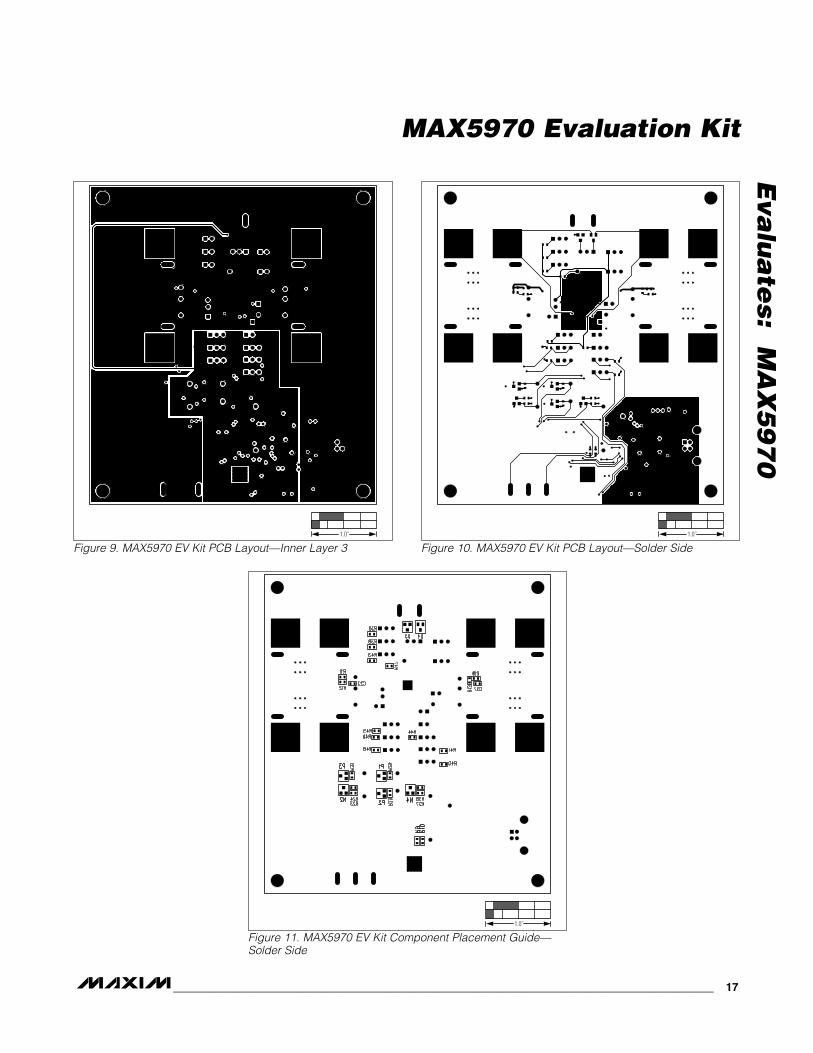
Figure 9. MAX5970 EV Kit PCB Layout—Inner Layer 3 Figure 10. MAX5970 EV Kit PCB Layout—Solder Side
Figure 11. MAX5970 EV Kit Component Placement Guide—Solder Side
1.0’’
1.0’’
1.0’’
Maxim cannot assume responsibility for use of any circuitry other than circuitry entirely embodied in a Maxim product. No circuit patent licenses are implied. Maxim reserves the right to change the circuitry and specifications without notice at any time.
18 Maxim Integrated Products, 120 San Gabriel Drive, Sunnyvale, CA 94086 408-737-7600© 2010 Maxim Integrated Products Maxim is a registered trademark of Maxim Integrated Products, Inc.
MAX5970 Evaluation Kit
Eva
lua
tes:
M
AX
59
70 Revision History
REVISIONNUMBER
REVISION DATE
DESCRIPTIONPAGES
CHANGED
0 04/10 Initial release —