max4475–max4478/max4488/max4489 - maxim … rail-to-rail op amps 19-2137; rev 7; 1/18 pin...
TRANSCRIPT
General DescriptionThe MAX4475–MAX4478/MAX4488/MAX4489 wide-band, low-noise, low-distortion operational amplifiers offer rail-to-rail outputs and single-supply operation down to 2.7V. They draw 2.2mA of quiescent supply current per amplifier while featuring ultra-low distortion (0.0002% THD+N), as well as low input voltage-noise density (4.5nV/√Hz) and low input current-noise density (0.5fA/√Hz). These features make the devices an ideal choice for applications that require low distortion and/or low noise.For power conservation, the MAX4475/MAX4488 offer a low-power shutdown mode that reduces supply cur-rent to 0.01µA and places the amplifiers’ outputs into a high-impedance state. These amplifiers have outputs which swing rail-to-rail and their input common-mode voltage range includes ground. The MAX4475–MAX4478 are unity-gain stable with a gain-bandwidth product of 10MHz. The MAX4488/4489 are internally compen-sated for gains of +5V/V or greater with a gain-band-width product of 42MHz. The single MAX4475/MAX4476/ MAX4488 are available in space-saving, 6-pin SOT23 and TDFN packages.
Applications ADC Buffers DAC Output Amplifiers Low-Noise Microphone/Preamplifiers Digital Scales Strain Gauges/Sensor Amplifiers Medical Instrumentation
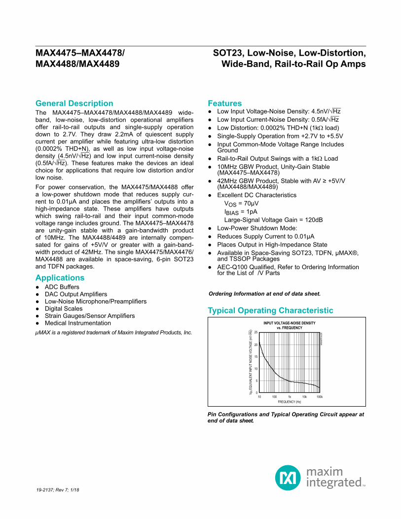
Features Low Input Voltage-Noise Density: 4.5nV/√Hz Low Input Current-Noise Density: 0.5fA/√Hz Low Distortion: 0.0002% THD+N (1kΩ load) Single-Supply Operation from +2.7V to +5.5V Input Common-Mode Voltage Range Includes
Ground Rail-to-Rail Output Swings with a 1kΩ Load 10MHz GBW Product, Unity-Gain Stable
(MAX4475–MAX4478) 42MHz GBW Product, Stable with AV ≥ +5V/V
(MAX4488/MAX4489) Excellent DC Characteristics
VOS = 70µV IBIAS = 1pA Large-Signal Voltage Gain = 120dB
Low-Power Shutdown Mode: Reduces Supply Current to 0.01µA Places Output in High-Impedance State Available in Space-Saving SOT23, TDFN, µMAX®,
and TSSOP Packages AEC-Q100 Qualified, Refer to Ordering Information
for the List of /V Parts
µMAX is a registered trademark of Maxim Integrated Products, Inc.
Ordering Information at end of data sheet.
25
20
10
5
010 1k 10k100 100k
INPUT VOLTAGE-NOISE DENSITYvs. FREQUENCY
MAX
4475
toc2
0
FREQUENCY (Hz)
15
V IN
EQUI
VALE
NT IN
PUT
NOIS
E VO
LTAG
E (n
V√Hz
)
MAX4475–MAX4478/MAX4488/MAX4489
SOT23, Low-Noise, Low-Distortion, Wide-Band, Rail-to-Rail Op Amps
19-2137; Rev 7; 1/18
Pin Configurations and Typical Operating Circuit appear at end of data sheet.
Typical Operating Characteristic

Power-Supply Voltage (VDD to VSS) ....................-0.3V to +6.0VAnalog Input Voltage (IN_+, IN_-) . (VSS - 0.3V) to (VDD + 0.3V)SHDN Input Voltage ..................................(VSS - 0.3V) to +6.0VOutput Short-Circuit Duration to Either Supply .........ContinuousContinuous Input Current (IN+, IN-) .................................±10mAContinuous Power Dissipation (TA = +70°C) 6-Pin SOT23 (derate 9.1mW/°C above +70°C) ..........727mW 6-Pin TDFN (derate 18.2mW/°C above 70°C) ..........1454mW 8-Pin µMAX (derate 4.5mW/°C above +70°C) ............362mW
8-Pin SO (derate 5.88mW/°C above +70°C) ...............471mW 14-Pin SO (derate 8.33mW/°C above +70°C) .............667mW 14-Pin TSSOP (derate 9.1mW/°C above +70°C) ........727mWOperating Temperature Range ......................... -40°C to +125°CJunction Temperature ......................................................+150°CStorage Temperature Range ............................ -65°C to +150°CLead Temperature (soldering, 10s) .................................+300°CSoldering Temperature (reflow) .......................................+260°C
(VDD = +5V, VSS = 0V, VCM = 0V, VOUT = VDD/2, RL tied to VDD/2, SHDN = VDD, TA = -40°C to +125°C, unless otherwise noted. Typical values are at TA = +25°C.) (Notes 1, 2)
PARAMETER SYMBOL CONDITIONS MIN TYP MAX UNITSSupply Voltage Range VDD (Note 3) 2.7 5.5 V
Quiescent Supply Current PerAmplifier ID
Normal modeVDD = 3V 2.2
mAVDD = 5V 2.5 4.4
Shutdown mode (SHDN = VSS) (Note 2) 0.01 1.0 µA
Input Offset Voltage VOSTA = +25°C ±70 ±350
µVTA = -40°C to +125°C ±750
Input Offset Voltage Tempco TCVOS ±0.3 ±6 µV/°CInput Bias Current IB (Note 4) ±1 ±150 pAInput Offset Current IOS (Note 4) ±1 ±150 pADifferential Input Resistance RIN 1000 GΩ
Input Common-Mode VoltageRange VCM
Guaranteed byCMRR Test
TA = +25°C -0.2 VDD - 1.6V
TA = -40°C to +125°C -0.1 VDD - 1.7
Common-Mode Rejection Ratio CMRR
(VSS - 0.2V) ≤VCM ≤ (VDD –1.6V)
TA = +25°C 90 115
dB(VSS - 0.1V) ≤VCM ≤ (VDD –1.7V)
TA = -40°C to +125°C 90
Power-Supply Rejection Ratio PSRR VDD = 2.7 to 5.5V 90 120 dB
Large-Signal Voltage Gain AVOL
RL = 10kΩ to VDD/2; VOUT = 100mV to (VDD - 125mV) 90 120
dBRL = 1kΩ to VDD/2; VOUT = 200mV to (VDD - 250mV) 85 110
RL = 500Ω to VDD/2; VOUT = 350mV to (VDD - 500mV) 85 110
www.maximintegrated.com Maxim Integrated 2
MAX4475–MAX4478/MAX4488/MAX4489
SOT23, Low-Noise, Low-Distortion, Wide-Band, Rail-to-Rail Op Amps
DC Electrical Characteristics
Stresses beyond those listed under “Absolute Maximum Ratings” may cause permanent damage to the device. These are stress ratings only, and functional operation of the device at these or any other conditions beyond those indicated in the operational sections of the specifications is not implied. Exposure to absolute maximum rating conditions for extended periods may affect device reliability.
Absolute Maximum Ratings

(VDD = +5V, VSS = 0V, VCM = 0V, VOUT = VDD/2, RL tied to VDD/2, SHDN = VDD, TA = +25°C.)
(VDD = +5V, VSS = 0V, VCM = 0V, VOUT = VDD/2, RL tied to VDD/2, SHDN = VDD, TA = -40°C to +125°C, unless otherwise noted. Typical values are at TA = +25°C.) (Notes 1, 2)
PARAMETER SYMBOL CONDITIONS MIN TYP MAX UNITS
Gain-Bandwidth Product GBWPMAX4475–MAX4478 AV = +1V/V 10
MHzMAX4488/MAX4489 AV = +5V/V 42
Slew Rate SRMAX4475–MAX4478 AV = +1V/V 3
V/µsMAX4488/MAX4489 AV = +5V/V 10
Full-Power Bandwidth (Note 5)MAX4475–MAX4478 AV = +1V/V 0.4
MHzMAX4488/MAX4489 AV = +5V/V 1.25
Peak-to-Peak Input Noise Voltage en(P-P) f = 0.1Hz to 10Hz 260 nVP-P
Input Voltage-Noise Density en
f = 10Hz 21nV/√Hzf = 1kHz 4.5
f = 30kHz 3.5Input Current-Noise Density in f = 1kHz 0.5 fA/√Hz
Total Harmonic Distortion Plus Noise (Note 6) THD + N
VOUT = 2VP-P,AV = +1V/V (MAX4475–MAX4478),RL = 10kΩ to GND
f = 1kHz 0.0002
%
f = 20kHz 0.0007
VOUT = 2VP-P,AV = +1V/V (MAX4475–MAX4478),RL = 1kΩ to GND
f = 1kHz 0.0002
f = 20kHz 0.001
VOUT = 2VP-P,AV = +5V/V (MAX4488/MAX4489),RL = 10kΩ to GND
f = 1kHz 0.0004
f = 20kHz 0.0006
PARAMETER SYMBOL CONDITIONS MIN TYP MAX UNITS
Output Voltage Swing VOUT
|VIN+ - VIN-| ≥ 10mV,RL = 10kΩ to VDD/2
VDD - VOH 10 45
mV
VOL - VSS 10 40
|VIN+ - VIN-| ≥ 10mV,RL = 1kΩ to VDD/2
VDD - VOH 80 200VOL - VSS 50 150
|VIN+ - VIN-| ≥ 10mV,RL = 500Ω to VDD/2
VDD - VOH 100 300VOL - VSS 80 250
Output Short-Circuit Current ISC 48 mA
Output Leakage Current ILEAKShutdown mode (SHDN = VSS),VOUT = VSS to VDD
±0.001 ±1.0 µA
SHDN Logic Low VIL 0.3 x VDD VSHDN Logic High VIH 0.7 x VDD VSHDN Input Current SHDN = VSS to VDD 0.01 1 µAInput Capacitance CIN 10 pF
www.maximintegrated.com Maxim Integrated 3
MAX4475–MAX4478/MAX4488/MAX4489
SOT23, Low-Noise, Low-Distortion, Wide-Band, Rail-to-Rail Op Amps
AC Electrical Characteristics
DC Electrical Characteristics (continued)

(VDD = +5V, VSS = 0V, VCM = 0V, VOUT = VDD/2, RL tied to VDD/2, input noise floor of test equipment =10nV/√Hz for all distortion measurements, TA = +25°C, unless otherwise noted.)
Note 1: All devices are 100% tested at TA = +25°C. Limits over temperature are guaranteed by design.Note 2: SHDN is available on the MAX4475/MAX4488 only.Note 3: Guaranteed by the PSRR test.Note 4: Guaranteed by design.Note 5: Full-power bandwidth for unity-gain stable devices (MAX4475–MAX4478) is measured in a closed-loop gain of +2V/V to
accommodate the input voltage range, VOUT = 4VP-P.Note 6: Lowpass-filter bandwidth is 22kHz for f = 1kHz and 80kHz for f = 20kHz. Noise floor of test equipment = 10nV/√Hz.
(VDD = +5V, VSS = 0V, VCM = 0V, VOUT = VDD/2, RL tied to VDD/2, SHDN = VDD, TA = +25°C.)
PARAMETER SYMBOL CONDITIONS MIN TYP MAX UNITS
Total Harmonic Distortion Plus Noise (Note 6) THD + N
VOUT = 2VP-P,AV = +5V/V(MAX4488/MAX4489),RL = 1kΩ to GND
f = 1kHz 0.0005%
f = 20kHz 0.008
Capacitive-Load Stability No sustained oscillations 200 pFGain Margin GM 12 dB
Phase Margin FMMAX4475–MAX4478, AV = +1V/V 70
degreesMAX4488/MAX4489, AV = +5V/V 80
Settling Time To 0.01%, VOUT = 2V step 2 µsDelay Time to Shutdown tSH 1.5 µsEnable Delay Time from Shutdown tEN VOUT = 2.5V, VOUT settles to 0.1% 10 µsPower-Up Delay Time VDD = 0 to 5V step, VOUT stable to 0.1% 13 µs
0
10
30
20
40
50
-0.5 1.50.5 2.5 3.5 4.5
INPUT OFFSET VOLTAGE vs. INPUT COMMON-MODE VOLTAGE
MAX
4475
toc0
3
INPUT COMMON-MODE VOLTAGE (V)
INPU
T OF
FSET
VOL
TAGE
(µV)
VDD = 3V
VDD = 5V
-250
-100
-150
-200
0
-50
200
150
100
50
250
-50 -25 0 25 50 75 100 125
OFFSET VOLTAGE vs. TEMPERATURE
MAX
4475
toc0
2
TEMPERATURE (°C)
INPU
T OF
FSET
VOL
TAGE
(µV)
VCOM = 0V
4
2
10
8
6
12
14
16
18
-50 -30 -20-40 -10 0 10 20 30 40 50
INPUT OFFSET VOLTAGE DISTRIBUTION
MAX
4475
-8 to
c1
VOS (µV)
PERC
ENTA
GE O
F UN
ITS
(%)
0
www.maximintegrated.com Maxim Integrated 4
MAX4475–MAX4478/MAX4488/MAX4489
SOT23, Low-Noise, Low-Distortion, Wide-Band, Rail-to-Rail Op Amps
Typical Operating Characteristics
AC Electrical Characteristics

(VDD = +5V, VSS = 0V, VCM = 0V, VOUT = VDD/2, RL tied to VDD/2, input noise floor of test equipment =10nV/√Hz for all distortion measurements, TA = +25°C, unless otherwise noted.)
0
1.0
0.5
2.0
1.5
2.5
3.0
-50 25 50-25 0 75 100 125
SUPPLY CURRENTvs. TEMPERATURE
MAX
4475
toc1
2
TEMPERATURE (°C)
SUPP
LY C
URRE
NT (m
A)
PER AMPLIFIER
50
70
60
100
90
80
130
120
110
140
-50 0 25-25 50 75 100 125
LARGE-SIGNAL VOLTAGE GAINvs. TEMPERATURE
MAX
4475
toc1
1
TEMPERATURE (°C)
A VOL
(dB)
RL = 100kΩ
RL = 10kΩ
VOUT = 150mV TO 4.75V50
60
70
80
90
100
110
120
130
0 50 100 150 200 250
LARGE-SIGNAL VOLTAGE GAINvs. OUTPUT VOLTAGE SWING
MAX
4475
toc1
0
VOUT SWING FROM EITHER SUPPLY (mV)
A V (d
B)
RL = 200kΩ
RL = 2kΩRL = 20kΩ
VDD = 5VRL REFERENCED TO VDD
50
60
70
80
90
100
110
120
130
0 50 100 150 200 250
LARGE-SIGNAL VOLTAGE GAINvs. OUTPUT VOLTAGE SWING
MAX
4475
toc0
9
VOUT SWING FROM EITHER SUPPLY (mV)
A V (d
B)
RL = 200kΩRL = 20kΩ
RL = 2kΩ
VDD = 5VRL REFERENCED TO GND
50
60
70
80
90
100
110
120
130
0 50 100 150 200 250
LARGE-SIGNAL VOLTAGE GAINvs. OUTPUT VOLTAGE SWING
MAX
4475
toc0
8
VOUT SWING FROM EITHER SUPPLY (mV)
A V (d
B)
RL = 200kΩRL = 20kΩ
RL = 2kΩ
VDD = 3VRL REFERENCED TO VDD
50
60
70
80
90
100
110
120
130
0 50 100 150 200 250
LARGE-SIGNAL VOLTAGE GAINvs. OUTPUT VOLTAGE SWING
MAX
4475
toc0
7
VOUT SWING FROM EITHER SUPPLY (mV)
A V (d
B)
RL = 200kΩRL = 20kΩRL = 2kΩ
VDD = 3VRL REFERENCED TO GND
0
20
10
40
30
60
50
70
-50 0 25-25 50 75 100 125
OUTPUT VOLTAGE SWING (VOL)vs. TEMPERATURE
MAX
4475
toc0
6
TEMPERATURE (°C)
V OL (
mV)
RL = 1kΩ
RL = 10kΩ0
20
10
40
30
60
50
70
-50 0 25-25 50 75 100 125
OUTPUT VOLTAGE SWING (VOH)vs. TEMPERATURE
MAX
4475
toc0
5
TEMPERATURE (°C)
V DD
- VOH
(mV)
RL = 1kΩ
RL = 10kΩ
0
0.05
0.10
0.15
0.20
0.25
0 4 52 31 6 7 8 9 10
OUTPUT VOLTAGE vs. OUTPUT LOAD CURRENT
MAX
4475
toc0
4
OUTPUT LOAD CURRENT (mA)
OUTP
UT V
OLTA
GE (V
)
VDD - VOH
VOL
VDD = 3V OR 5VVDIFF = 10mV
Maxim Integrated 5www.maximintegrated.com
MAX4475–MAX4478/MAX4488/MAX4489
SOT23, Low-Noise, Low-Distortion, Wide-Band, Rail-to-Rail Op Amps
Typical Operating Characteristics (continued)
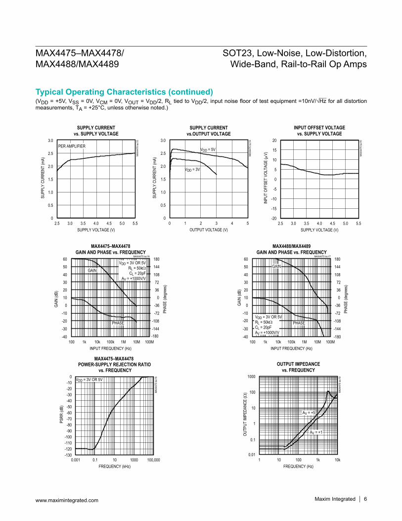
(VDD = +5V, VSS = 0V, VCM = 0V, VOUT = VDD/2, RL tied to VDD/2, input noise floor of test equipment =10nV/√Hz for all distortion measurements, TA = +25°C, unless otherwise noted.)
1000
100
10
1
0.1
0.011 100 1k10 10k
OUTPUT IMPEDANCEvs. FREQUENCY
MAX
4475
toc1
9
FREQUENCY (Hz)
OUTP
UT IM
PEDA
NCE
(Ω)
AV = +5
AV = +1
1000 100,000-130
-10-20-30-40-50-60-70-80-90
-100-110-120
0
0.001 0.1 10
MAX4475–MAX4478 POWER-SUPPLY REJECTION RATIO
vs. FREQUENCY
MAX
4475
toc1
8
FREQUENCY (kHz)
PSRR
(dB)
VDD = 3V OR 5V
MAX4488/MAX4489GAIN AND PHASE vs. FREQUENCY
INPUT FREQUENCY (Hz)100 100k 1M 10M1k 10k 100M
GAIN
(dB)
60
-40
-30
-20-10
0
10
20
50
40
30
-180
PHAS
E (d
egre
es)
180
-144
-108
-72
-36
0
36
144
108
72
MAX4475 toc17
VDD = 3V OR 5VRL = 50kΩCL = 20pFAV = +1000V/V
GAIN
PHASE
MAX4475–MAX4478GAIN AND PHASE vs. FREQUENCY
INPUT FREQUENCY (Hz)100 100k 1M 10M1k 10k 100M
GAIN
(dB)
60
-40
-30
-20
-10
0
10
20
50
40
30
-180
PHAS
E (d
egre
es)
180
-144
-108
-72
-36
0
36
144
108
72
MAX4475 toc16
VDD = 3V OR 5VRL = 50kΩCL = 20pF
AV = +1000V/V
GAIN
PHASE
-20
-15
-10
-5
0
5
10
15
20
2.5 3.53.0 4.0 4.5 5.0 5.5
INPUT OFFSET VOLTAGEvs. SUPPLY VOLTAGE
MAX
4475
toc1
5
SUPPLY VOLTAGE (V)
INPU
T OF
FSET
VOL
TAGE
(µV)
0
1.0
0.5
2.0
1.5
2.5
3.0
0 21 3 4 5
SUPPLY CURRENTvs.OUTPUT VOLTAGE
MAX
4475
toc1
4
OUTPUT VOLTAGE (V)
SUPP
LY C
URRE
NT (m
A)VDD = 5V
VDD = 3V
0
1.0
0.5
2.0
1.5
2.5
3.0
2.5 3.5 4.03.0 4.5 5.0 5.5
SUPPLY CURRENTvs. SUPPLY VOLTAGE
MAX
4475
toc1
3
SUPPLY VOLTAGE (V)
SUPP
LY C
URRE
NT (m
A)
PER AMPLIFIER
Maxim Integrated 6www.maximintegrated.com
MAX4475–MAX4478/MAX4488/MAX4489
SOT23, Low-Noise, Low-Distortion, Wide-Band, Rail-to-Rail Op Amps
Typical Operating Characteristics (continued)

(VDD = +5V, VSS = 0V, VCM = 0V, VOUT = VDD/2, RL tied to VDD/2, input noise floor of test equipment =10nV/√Hz for all distortion measurements, TA = +25°C, unless otherwise noted.)
4µs/div
MAX4475–MAX4478SMALL-SIGNAL PULSE RESPONSE
VDD = 3V, RL = 10kΩ, CL = 100pFVIN = 100mV PULSE
0.5V
MAX4475 toc28
0.6V
20mV/div
1µs/div
MAX4475–MAX4478LARGE-SIGNAL PULSE RESPONSE
VDD = 3V, RL = 10kΩ, CL = 100pFVIN = 2V
0.5V
MAX4475 toc27
2.5V
1
0.00010 5k 15k 20k
MAX4488/MAX4489TOTAL HARMONIC DISTORTION PLUS NOISE
vs. FREQUENCY
0.001
0.01
0.1
MAX
4475
toc2
6
FREQUENCY (Hz)
THD
+ N
(%)
10k
FILTER BW = 80kHzRL = 10kΩ TO GNDR1 = 2.43kΩ, R2 = 10kΩVOUT = 2.75VP-P
AV = +5, VDD = 3V
AV = +5, VDD = 5V
0.01
0.0010 20k
MAX4475–MAX4478TOTAL HARMONIC DISTORTION PLUS NOISE
vs. FREQUENCY
MAX
4475
toc2
5
FREQUENCY (Hz)
THD
+ N
(%)
5k 10k 15k
FILTER BW = 80kHzVOUT = 2VP-PAV = +1RL = 1kΩ
RL TO VDD/2 RL TO GND
RL TO VDD
0.01
0.00010 10k 20k
MAX4488/MAX4489TOTAL HARMONIC DISTORTION PLUS NOISE vs. FREQUENCY
MAX
4475
toc2
4
FREQUENCY (Hz)
THD
+ N
(%)
0.001
5k 15k
FILTER BW = 22kHzRL = 10kΩ TO GNDR1 = 5.6kΩ, R2 = 53kΩVOUT = 2VP-P
AV = +10, VDD = 3V
AV = +10, VDD = 5V
MAX4488/MAX4489TOTAL HARMONIC DISTORTION PLUS NOISE
vs. OUTPUT VOLTAGE SWING
OUTPUT VOLTAGE (VP-P)0 21 3
THD
+ N
(%)
10
0.00001
0.0001
0.001
0.01
1
0.1
MAX
4475
toc2
3
VDD = +3V, fO = 20kHzFILTER BW = 80kHz
VDD = 3V, fO = 3kHzFILTER BW = 30kHz
AV = +5RL = 100kΩ
MAX4475TOTAL HARMONIC DISTORTION PLUS NOISE
vs. OUTPUT VOLTAGE SWING
MAX
4475
toc2
2
OUTPUT VOLTAGE (VP-P)
THD
+ N
(%)
10
0.0001
0.001
0.01
0.1
1
0 21 3 4
fO = 20kHz, FILTER BW = 80kHz
fO = 3kHz, FILTER BW = 30kHz
AV = +1RL = 100kΩ
1s/div
0.1Hz TO 10HzP-P NOISE
VDD = 3V OR 5VVP-P NOISE = 260nVP-P
200nV/div
MAX4475 toc2125
20
10
5
010 1k 10k100 100k
INPUT VOLTAGE-NOISE DENSITYvs. FREQUENCY
MAX
4475
toc2
0
FREQUENCY (Hz)
15
V IN
EQUI
VALE
NT IN
PUT
NOIS
E VO
LTAG
E (n
V√Hz
)
Maxim Integrated 7www.maximintegrated.com
MAX4475–MAX4478/MAX4488/MAX4489
SOT23, Low-Noise, Low-Distortion, Wide-Band, Rail-to-Rail Op Amps
Typical Operating Characteristics (continued)

(VDD = +5V, VSS = 0V, VCM = 0V, VOUT = VDD/2, RL tied to VDD/2, input noise floor of test equipment =10nV/√Hz for all distortion measurements, TA = +25°C, unless otherwise noted.)
PIN
NAME FUNCTIONMAX4475/MAX4488
MAX4475/MAX4488 MAX4476 MAX4477/
MAX4489 MAX4478
SOT23/TDFN SO/µMAX SOT23/TDFN SO/µMAX SO/TSSOP
1 6 1 1, 7 1, 7, 8, 14OUT, OUTA,
OUTB, OUTC,OUTD
Amplifier Output
2 4 2 4 11 VSSNegative Supply. Connectto ground for single-supplyoperation
3 3 3 3, 5 3, 5, 10, 12 IN+, INA+, INB+,INC+, IND+
Noninverting AmplifierInput
4 2 4 2, 6 2, 6, 9, 13 IN-, INA-, INB-,INC-, IND- Inverting Amplifier Input
6 7 6 8 4 VDD Positive Supply
5 8 — — — SHDN
Shutdown Input. Connectto VDD for normaloperation (amplifier(s)enabled).
— 1, 5 5 — — N.C. No Connection. Notinternally connected.
EP — EP — — EP Exposed Paddle (TDFNOnly). Connect to VSS.
-20
-9010 1000100 100k 100M10M
MAX4477/MAX4478/MAX4489CROSSTALK vs. FREQUENCY
-60
-50
-40
-30
MAX
4475
toc3
1
FREQUENCY (Hz)
CROS
STAL
K (d
B)
10k 1M
-70
-80
1µs/div
MAX4488/MAX4489SMALL-SIGNAL PULSE RESPONSE
VDD = 3V, RL = 10kΩ, CL = 50pFVIN = 20mV PULSE, AV = +5V/V
MAX4475 toc30
VOUT50mV/div
1.6V
1.5V
1µs/div
MAX4488/MAX4489LARGE-SIGNAL PULSE RESPONSE
VDD = 3V, RL = 10kΩ, CL = 50pFVIN = 20mV PULSE, AV = +5V/V
MAX4475 toc29
VOUT200mV/div
Maxim Integrated 8www.maximintegrated.com
MAX4475–MAX4478/MAX4488/MAX4489
SOT23, Low-Noise, Low-Distortion, Wide-Band, Rail-to-Rail Op Amps
Pin Description
Typical Operating Characteristics (continued)

Detailed DescriptionThe MAX4475–MAX4478/MAX4488/MAX4489 single- supply operational amplifiers feature ultra-low noise and distortion. Their low distortion and low noise make them ideal for use as preamplifiers in wide dynamic-range appli-cations, such as 16-bit analog-to-digital converters (see Typical Operating Circuit). Their high-input impedance and low noise are also useful for signal conditioning of high-im-pedance sources, such as piezoelectric transducers.These devices have true rail-to-rail output operation, drive loads as low as 1kΩ while maintaining DC accuracy, and can drive capacitive loads up to 200pF without oscillation. The input common-mode voltage range extends from (VDD - 1.6V) to 200mV below the negative rail. The push-pull output stage maintains excellent DC characteristics, while delivering up to ±5mA of current.The MAX4475–MAX4478 are unity-gain stable, while the MAX4488/MAX4489 have a higher slew rate and are stable for gains ≥ 5V/V. The MAX4475/MAX4488 feature a low-power shutdown mode, which reduces the supply current to 0.01µA and disables the outputs.
Low DistortionMany factors can affect the noise and distortion that the device contributes to the input signal. The following guide-lines offer valuable information on the impact of design choices on Total Harmonic Distortion (THD).Choosing proper feedback and gain resistor values for a particular application can be a very important factor in reducing THD. In general, the smaller the closed-loop gain, the smaller the THD generated, especially when driving heavy resistive loads. The THD of the part nor-mally increases at approximately 20dB per decade, as a function of frequency. Operating the device near or above the full-power bandwidth significantly degrades distortion.Referencing the load to either supply also improves the part’s distortion performance, because only one of the MOSFETs of the push-pull output stage drives the output. Referencing the load to midsupply increases the part’s distortion for a given load and feedback setting. (See the Total Harmonic Distortion vs. Frequency graph in the Typical Operating Characteristics.)For gains ≥ 5V/V, the decompensated devices MAX4488/MAX4489 deliver the best distortion performance, since they have a higher slew rate and provide a higher amount of loop gain for a given closed-loop gain setting. Capacitive loads below 100pF do not significantly affect distortion results. Distortion performance is relatively con-stant over supply voltages.
Figure 2b. Pulse Response with 10pF Feed-Forward Compensation
Figure 2a. Pulse Response with No Feed-Forward Compensation
Figure 1. Adding Feed-Forward Compensation
VOUT100mV/div
VIN100mV/div
AV = +2RF = RG = 100kΩ
2µs/div
VOUT100mV/div
VIN100mV/div
100mV
0V
AV = +2RF = RG = 100kΩ
2µs/div
CZ
RF
VOUT
VIN
RG
www.maximintegrated.com Maxim Integrated 9
MAX4475–MAX4478/MAX4488/MAX4489
SOT23, Low-Noise, Low-Distortion, Wide-Band, Rail-to-Rail Op Amps

Ground-Sensing and Rail-to-Rail OutputsThe common-mode input range of these devices extends below ground, and offers excellent common-mode rejec-tion. These devices are guaranteed not to undergo phase reversal when the input is overdriven (Figure 3).Figure 4 showcases the true rail-to-rail output operation of the amplifier, configured with AV = 5V/V. The output swings to within 8mV of the supplies with a 10kΩ load, making the devices ideal in low-supply voltage applica-tions.
Power Supplies and LayoutThe MAX4475–MAX4478/MAX4488/MAX4489 operate from a single +2.7V to +5.5V power supply or from dual supplies of ±1.35V to ±2.75V. For single-supply opera-tion, bypass the power supply with a 0.1µF ceramic
Low NoiseThe amplifier’s input-referred noise-voltage density is dominated by flicker noise at lower frequencies, and by thermal noise at higher frequencies. Because the thermal noise contribution is affected by the parallel combination of the feedback resistive network (RF || RG, Figure 1), these resistors should be reduced in cases where the system bandwidth is large and thermal noise is dominant. This noise contribution factor decreases, however, with increasing gain settings.For example, the input noise-voltage density of the circuit with RF = 100kΩ, RG = 11kΩ (AV = +5V/V) is en = 14nV/√Hz, en can be reduced to 6nV/√Hz by choos-ing RF = 10kΩ, RG = 1.1kΩ (AV = +5V/V), at the expense of greater current consumption and potentially higher distortion. For a gain of 100V/V with RF = 100kΩ, RG = 1.1kΩ, the en is still a low 6nV/√Hz.
Using a Feed-Forward Compensation Capacitor, CZThe amplifier’s input capacitance is 10pF. If the resistance seen by the inverting input is large (feedback network), this can introduce a pole within the amplifier’s bandwidth resulting in reduced phase margin. Compensate the reduced phase margin by introducing a feed-forward capacitor (CZ) between the inverting input and the out-put (Figure 1). This effectively cancels the pole from the inverting input of the amplifier. Choose the value of CZ as follows:
CZ = 10 x (RF / RG) [pF]In the unity-gain stable MAX4475–MAX4478, the use of a proper CZ is most important for AV = +2V/V, and AV = -1V/V. In the decompensated MAX4488/MAX4489, CZ is most important for AV = +10V/V. Figures 2a and 2b show transient response both with and without CZ.Using a slightly smaller CZ than suggested by the formula above achieves a higher bandwidth at the expense of reduced phase and gain margin. As a general guideline, consider using CZ for cases where RG || RF is greater than 20kΩ (MAX4475–MAX4478) or greater than 5kΩ (MAX4488/MAX4489).
Applications InformationThe MAX4475–MAX4478/MAX4488/MAX4489 combine good driving capability with ground-sensing input and rail-to-rail output operation. With their low distortion and low noise, they are ideal for use in ADC buffers, medical instrumentation systems and other noise-sensitive appli-cations.
Figure 4. Rail-to-Rail Output Operation
Figure 3. Overdriven Input Showing No Phase Reversal
VOUT1V/div
5V
0V
20ms/div
VOUT2V/div
VIN2V/div
0V
AV = +1VDD = +5VRL = 10kΩ
40µs/div
www.maximintegrated.com Maxim Integrated 10
MAX4475–MAX4478/MAX4488/MAX4489
SOT23, Low-Noise, Low-Distortion, Wide-Band, Rail-to-Rail Op Amps

capacitor placed close to the VDD pin. If operating from dual supplies, bypass each supply to ground.Good layout improves performance by decreasing the amount of stray capacitance and noise at the op amp’s inputs and output. To decrease stray capacitance, mini-mize PC board trace lengths and resistor leads, and place external components close to the op amp’s pins.
Typical Application CircuitThe Typical Application Circuit shows the sin-gle MAX4475 configured as an output buffer for the MAX5541 16-bit DAC. Because the MAX5541 has an unbuffered voltage output, the input bias current of the op amp used must be less than 6nA to maintain 16-bit accuracy. The MAX4475 has an input bias current of only 150pA (max), virtually eliminating this as a source
of error. In addition, the MAX4475 has excellent open-loop gain and common-mode rejection, making this an excellent output buffer amplifier.
DC-Accurate Lowpass FilterThe MAX4475–MAX4478/MAX4488/MAX4489 offer a unique combination of low noise, wide bandwidth, and high gain, making them an excellent choice for active filters up to 1MHz. The Typical Operating Circuit shows the dual MAX4477 configured as a 5th order Chebyschev filter with a cutoff frequency of 100kHz. The circuit is implemented in the Sallen-Key topology, making this a DC-accurate filter.
1
2
3
4
5
6
7
8
470pF
3.09kΩ1%
3.83kΩ1%
13.7kΩ1%
7.87kΩ1%
10.0kΩ1%
10.0kΩ1%
15.0kΩ1%
7.15kΩ1%
10.0kΩ1%
0.1µF
220pF
220pF
220pF
220pF
5V
MAX44771/2
MAX44771/2
0 to +2.5VOUTPUT
SHDN
84
CS
SCLK
DIN2
3SERIAL INTERFACE
VDD
DGND
REF
OUT
AGND
+5V +2.5V +5V
7
6
U1MAX5541ESA
U2MAX4475AUA
www.maximintegrated.com Maxim Integrated 11
MAX4475–MAX4478/MAX4488/MAX4489
SOT23, Low-Noise, Low-Distortion, Wide-Band, Rail-to-Rail Op Amps
Typical Operating Circuit
Typical Application Circuit

OUT
N.C.VSS
+
+
+
+
2
8
7 VDDINA-
INA+
N.C.
SO/MAX
TOP VIEW
3
4
6
5
MAX4475MAX4488
SHDN+
INB-
OUTB
INB+VSS
1
2
8
7
VDD
INA-
INA+
OUTA
SO/MAX
TOP VIEW
3
4
6
5
MAX4477MAX4489
14
13
12
11
10
9
8
1
2
3
4
5
6
7
OUTD
IND-
IND+
VSSVDD
INA+
INA-
OUTA
TOP VIEW
MAX4478
INC+
INC-
OUTCOUTB
INB-
INB+
SO/TSSOP
VSS
IN-IN+
1 6 VDD
5
OUT
MAX4475MAX4488
SOT23-6
TOP VIEW
2
3 4
SHDN
N.C.VSS
IN-IN+
1 6 VDDOUT
MAX4476
SOT23-6
TOP VIEW
2
3 4
5
MAX4475MAX4488
TOP VIEW6
V DD
5
SHDN
4
IN-
OUT
V SS
IN+
1 2 3
TDFN
EP
+
MAX4476
TOP VIEW6
V DD
5
N.C.
4IN
-
OUT
V SS
IN+
1 2 3
TDFN
EP
+
www.maximintegrated.com Maxim Integrated 12
MAX4475–MAX4478/MAX4488/MAX4489
SOT23, Low-Noise, Low-Distortion, Wide-Band, Rail-to-Rail Op Amps
Pin Configurations
+Denotes a lead(Pb)-free/RoHS-compliant package.*EP = Exposed pad (connect to VSS)./V denotes an automotive qualified part.T = Tape and reel.
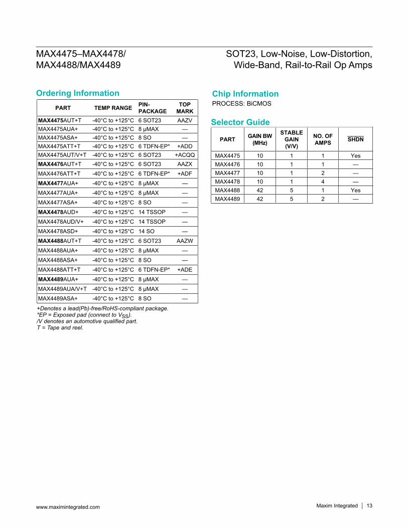
PART GAIN BW(MHz)
STABLEGAIN(V/V)
NO. OFAMPS SHDN
MAX4475 10 1 1 YesMAX4476 10 1 1 —MAX4477 10 1 2 —MAX4478 10 1 4 —MAX4488 42 5 1 YesMAX4489 42 5 2 —
Selector Guide
PART TEMP RANGE PIN-PACKAGE
TOPMARK
MAX4475AUT+T -40°C to +125°C 6 SOT23 AAZVMAX4475AUA+ -40°C to +125°C 8 µMAX —MAX4475ASA+ -40°C to +125°C 8 SO —MAX4475ATT+T -40°C to +125°C 6 TDFN-EP* +ADDMAX4475AUT/V+T -40°C to +125°C 6 SOT23 +ACQQMAX4476AUT+T -40°C to +125°C 6 SOT23 AAZXMAX4476ATT+T -40°C to +125°C 6 TDFN-EP* +ADFMAX4477AUA+ -40°C to +125°C 8 µMAX —MAX4477AUA+ -40°C to +125°C 8 µMAX —MAX4477ASA+ -40°C to +125°C 8 SO —MAX4478AUD+ -40°C to +125°C 14 TSSOP —MAX4478AUD/V+ -40°C to +125°C 14 TSSOP —MAX4478ASD+ -40°C to +125°C 14 SO —MAX4488AUT+T -40°C to +125°C 6 SOT23 AAZWMAX4488AUA+ -40°C to +125°C 8 µMAX —MAX4488ASA+ -40°C to +125°C 8 SO —MAX4488ATT+T -40°C to +125°C 6 TDFN-EP* +ADEMAX4489AUA+ -40°C to +125°C 8 µMAX —MAX4489AUA/V+T -40°C to +125°C 8 µMAX —MAX4489ASA+ -40°C to +125°C 8 SO —
www.maximintegrated.com Maxim Integrated 13
MAX4475–MAX4478/MAX4488/MAX4489
SOT23, Low-Noise, Low-Distortion, Wide-Band, Rail-to-Rail Op Amps
Chip InformationPROCESS: BiCMOS
Ordering Information

PACKAGE TYPE PACKAGE CODE OUTLINE NO. LANDPATTERN NO.
6 SOT23 U6F+6 21-0058 90-01758 µMAX U8+1 21-0036 90-0092
14 TSSOP U14+2 21-0066 90-01178 SO S8+4 21-0041 —14 SO S14+4 21-0041 —
6 TDFN-EP T633+2 21-0137 90-0058
www.maximintegrated.com Maxim Integrated 14
MAX4475–MAX4478/MAX4488/MAX4489
SOT23, Low-Noise, Low-Distortion, Wide-Band, Rail-to-Rail Op Amps
Package InformationFor the latest package outline information and land patterns (footprints), go to www.maximintegrated.com/packages. Note that a “+”, “#”, or “-” in the package code indicates RoHS status only. Package drawings may show a different suffix character, but the drawing pertains to the package regardless of RoHS status.

REVISION NUMBER
REVISION DATE DESCRIPTION PAGES
CHANGED
4 12/09 Added lead-free designations and an automotive part to the Ordering Information and added input current spec in Absolute Maximum Ratings section 1, 2, 13
5 7/10 Added /V designation to the MAX4475 product and soldering temperature 1, 26 6/12 Added /V designation for MAX4489. 137 1/18 Added AEC statement to Features section 1
Maxim Integrated cannot assume responsibility for use of any circuitry other than circuitry entirely embodied in a Maxim Integrated product. No circuit patent licenses are implied. Maxim Integrated reserves the right to change the circuitry and specifications without notice at any time. The parametric values (min and max limits) shown in the Electrical Characteristics table are guaranteed. Other parametric values quoted in this data sheet are provided for guidance.
Maxim Integrated and the Maxim Integrated logo are trademarks of Maxim Integrated Products, Inc. © 2018 Maxim Integrated Products, Inc. 15
MAX4475–MAX4478/MAX4488/MAX4489
SOT23, Low-Noise, Low-Distortion, Wide-Band, Rail-to-Rail Op Amps
Revision History
For pricing, delivery, and ordering information, please contact Maxim Direct at 1-888-629-4642, or visit Maxim Integrated’s website at www.maximintegrated.com.