max40000max40001 1.v, nanopoer comparators it … description the max40000/max40001 are tiny, single...
TRANSCRIPT

General DescriptionThe MAX40000/MAX40001 are tiny, single comparators with built-in voltage references that are ideal for a wide variety of portable electronics applications, such as cell phones, portable instruments, and notebooks that have extremely tight board space and power constraints. The MAX40000/MAX40001 are available in a 6-bump wafer-level package (WLP) with 1.11mm x 0.76mm footprint and a 6-pin SOT23 package. The MAX40000 has a push-pull output and the MAX40001 has an open-drain output.The devices offer a supply voltage range from 1.7V to 5.5V and consume only 0.9µA of supply current. They also feature internal filtering to provide high RF immunity, important in many portable applications.The devices have a high-precision integrated reference that is factory trimmed to an initial accuracy of 1% and better than 2.5% over the entire temperature range. Internal reference voltage options include 1.252V, 1.66V, 1.94V, and 2.22V. See Ordering Information for help with ordering a MAX40000/MAX40001 with a particular voltage reference value and package type. The reference output is stable for capacitive loads up to 100pF.These devices are fully specified over -40°C to +125°C automotive temperature range.
Applications Cell Phones Tablets and Consumer Accessories Notebook Computers Electronic Toys Portable Medical Instruments/Wearables Level Detectors
Benefits and Features Micropower Operating Current (0.9µA typ, 1.7µA max)
Preserves Battery Power Tiny 1.11mm x 0.76mm 6-Bump WLP and SOT23
Packages Save Board Space Internal Precision Reference Saves Space and Cost
of an External Reference• < 1% at Room Temperature, < 2.5% Over Temp
Reference• Multiple Reference Voltages (1.252V, 1.66V, 1.94V,
and 2.22V) Input Voltage Range = -0.2V to 5.7V Supply Voltage Range (1.7V to 5.5V) Allows
Operation from 1.8V, 2.5V, 3V, and 5V Supplies < 10µs Propagation Delay Push-Pull (MAX40000) or Open-Drain (MAX40001)
Outputs
Ordering Information appears at end of data sheet.
19-8610; Rev 4; 8/17
MAX40000/MAX40001 1.7V, nanoPower Comparators with Built-In Reference
EVALUATION KIT AVAILABLE

VDD to GND ...........................................................-0.3V to +6VREF to GND ............................................................-0.3V to +6VIP, IM to GND .........................................................-0.3V to +6VIP to IM .................................................................................±6VOUT (open-drain) to GND ......................................-0.3V to +6VOUT (push-pull) to GND .............................-0.3V to VDD + 0.3VOutput Short-Circuit Duration ................................................ 10sContinuous Current Into Any Input Pin .............................. .20mAContinuous Current Into/Out of Any Output Pin ................ .50mA
Continuous Power Dissipation (TA = +70°C) Maximum Power Dissipation (WLP, derate 10.2mW/°C above +70°C) .....................816mW
Maximum Power Dissipation (SOT23, derate 4.3mW/°C above +70°C) ................347.8mW
Operating Temperature Range ......................... -40°C to +125°CJunction Temperature (TJMAX) ........................................+150°CStorage Temperature Range ............................ -65°C to +150°CLead Temperature (soldering, 10s) .................................+300°CSoldering Temperature (reflow) .......................................+260°C
WLP Junction-to-Ambient Thermal Resistance (θJA) ..........98°C/W
SOT23 Junction-to-Ambient Thermal Resistance (θJA) ........230°C/W Junction-to-Case Thermal Resistance (θJC) ..............76°C/W
(Note 1)
(VDD = 3.3V, VCM = 0V, RPULLUP = 100kΩ from OUT to VPULLUP = 3.3V (for MAX40001 only), TA = TMIN to TMAX. Typical values are at TA = +25°C, unless otherwise noted.) (Note 2)
PARAMETER SYMBOL CONDITIONS MIN TYP MAX UNITS
POWER SUPPLY VOLTAGE
VDD Supply Voltage Range VDD
VREF < 1.8V, guaranteed by PSRR specification 1.7 5.5
VVREF > 1.8V, guaranteed by PSRR specification
VREF + 0.1 5.5
VDD Supply Current IDDNo output or reference load current,TA = -40°C to +125°C 0.9 1.7 µA
Power-Up Time 5 µs
COMPARATOR
Input Common-Mode Voltage Range VCM
TA = +25°C -0.2 VDD + 0.2 V
TA = -40°C to +125°C 0 VDD
Input Offset Voltage VOS
VCM = 0V to VDD -1V (Note 3) 8
mVVCM = VDD -1 to VDD, TA = 0°C to +85°C (Note 3)
10
VCM = VDD -1 to VDD, TA = -40°C to +125°C (Note 3)
14
Input Offset Drift 27 µV/°C
Input Hysteresis VHYS (Note 4) 2.5 mV
MAX40000/MAX40001 1.7V, nanoPower Comparators with Built-In Reference
www.maximintegrated.com Maxim Integrated 2
Note 1: Package thermal resistances were obtained using the method described in JEDEC specification JESD51-7, using a four-layer board. For detailed information on package thermal considerations, refer to www.maximintegrated.com/thermal-tutorial.
Absolute Maximum Ratings
Stresses beyond those listed under “Absolute Maximum Ratings” may cause permanent damage to the device. These are stress ratings only, and functional operation of the device at these or any other conditions beyond those indicated in the operational sections of the specifications is not implied. Exposure to absolute maximum rating conditions for extended periods may affect device reliability.
Package Thermal Characteristics
Electrical Characteristics

(VDD = 3.3V, VCM = 0V, RPULLUP = 100kΩ from OUT to VPULLUP = 3.3V (for MAX40001 only), TA = TMIN to TMAX. Typical values are at TA = +25°C, unless otherwise noted.) (Note 2)
PARAMETER SYMBOL CONDITIONS MIN TYP MAX UNITS
Input Bias CurrentVCM = -0.2V to VDD +0.2V, TA = 25°C
1 5 nAVCM = 0V to VDD, TA = -40°C to +85°C
VCM = 0.2V to VDD, TA = -40°C to +125°C
Input Offset Current 5 nA
Input Capacitance Either input, over VCM range 1.5 pF
Power Supply Rejection Ratio PSRR DC, over the entire common mode input
voltage range 60 dB
Common Mode Rejection Ratio CMRR DC, over the entire common mode input
voltage range 46 dB
Output Voltage Swing Low VOL Sinking 2mA output current, VOUT - VGND 0.4 V
Output Voltage Swing High VOHSourcing 2mA output current, VDD - VOUT
0.4 V
Output Leakage Current IO-LKGOpen-drain only (MAX40001), VDD = 1.8V, VO = 5.5V, TA = -40°C to +125°C 100 nA
Propagation Delay (Note 5) tPD
100mV overdrive, output L->H, MAX40000 9.6
µs
100mV overdrive, output L->H, MAX40001, 100kΩ 14
100mV overdrive, output H->L, MAX40000 3.2
20mV overdrive, output L->H, MAX40000 9.9
20mV overdrive, output L->H, MAX40001, 100kΩ 14.8
20mV overdrive, output H->L, MAX40000 5.2
Rise Time tR Push-pull output stage. 25% to 75% 300 ns
Fall Time tF 25% to 75% 52 ns
MAX40000/MAX40001 1.7V, nanoPower Comparators with Built-In Reference
www.maximintegrated.com Maxim Integrated 3
Electrical Characteristics (continued)

(VDD = 3.3V, VCM = 0V, RPULLUP = 100kΩ from OUT to VPULLUP = 3.3V (for MAX40001 only), TA = TMIN to TMAX. Typical values are at TA = +25°C, unless otherwise noted.) (Note 2)
Note 2: All specifications are 100% production tested at TA = +25°C. Specification limits over temperature (TA = TMIN to TMAX) are guaranteed by design, not production tested.
Note 3: Input offset voltage; VOS is defined as the center of the hysteresis band or average of the threshold trip points.Note 4: The hysteresis-related trip points are defined as the edges of the hysteresis band, measured with respect to the center of
the band (i.e., VOS) (Figure 1).Note 5: Specified with an input overdrive (VOVERDRIVE) of 100mV and 20mV, and load capacitance of CL = 15pF. VOVERDRIVE is
defined above the offset voltage and hysteresis of the comparator input. For the MAX40000/MAX40001, reference voltage error should also be added.
PARAMETER SYMBOL CONDITIONS MIN TYP MAX UNITSINTERNAL REFERENCE VOLTAGE
Reference Voltage VREF
TA = +25°C
MAX40000ANT12+T 1.2395 1.252 1.2645
VMAX4000_ _ _ _16+ 1.66
MAX4000_ _ _ _19+ 1.94
MAX4000_ _ _ _22+ 2.22
TA = -40°C to +85°C
MAX4000_ _ _ _12+ 1.252
VMAX4000_ _ _ _16+ 1.66
MAX4000_ _ _ _19+ 1.94
MAX4000_ _ _ _22+ 2.22
TA = -40°C to +125°C
MAX40000ANT12+T 1.2207 1.252 1.2833
VMAX4000_ _ _ _16+ 1.66
MAX4000_ _ _ _19+ 1.94
MAX4000_ _ _ _22+ 2.22
Reference Thermal Drift VREF-TEMPCO
Over extended temperature range, TA = -40°C to +125°C
15 ppm/°C
Line Regulation 1200 ppm/V
Load Regulation IVREFOUT = ±100nA 0.01 mV/nA
Output Current 0.1 µA
Voltage Noise 0.1 to 10Hz 82 µVP-PVoltage Noise Density CREF = 1nF 10Hz to 6kHz 2.19 µV/√Hz
Capacitive Load Stability 100 pF
MAX40000/MAX40001 1.7V, nanoPower Comparators with Built-In Reference
www.maximintegrated.com Maxim Integrated 4
Electrical Characteristics (continued)

(VDD = 3.3V, RPULLUP = 100kΩ from OUT to VPULLUP = 3.3V (for MAX40001 only), TA = +25°C, unless otherwise noted.)
0
10
20
30
0.1 1 10 100
SUPP
LYCU
RREN
T(μ
A)
OUTPUT TRANSISTION FREQUENCY(kHz)
toc04
VDD = 5.5V
RED =+125°CORANGE = +85°CGREEN = +25°CBLUE = -40°C
0
0.4
0.8
1.2
1.6
2
1.5 2 2.5 3 3.5 4 4.5 5 5.5
SUPP
LYCU
RREN
T(μ
A)
SUPPLY VOLTAGE (V)
toc01
VOUT = LOW
TA = -40°CTA = +25°C
TA = +85°C
0
10
20
30
40
50
0.1 1 10 100
SUP
PLY
CUR
RENT
(μA)
OUTPUT TRANSISTION FREQUENCY(kHz)
toc02
VDD = 1.7V
TA = +25°C
TA = -40°C
TA = +85°C
TA = +125°C
0
10
20
30
40
50
0.1 1 10 100
SU
PP
LYC
UR
REN
T(μ
A)
OUTPUT TRANSISTION FREQUENCY (kHz)
toc03
VDD = 3.3V
TA = +25°C
TA = -40°C
TA = +125°C
TA = +85°C
Maxim Integrated 5www.maximintegrated.com
MAX40000/MAX40001 1.7V, nanoPower Comparators with Built-In Reference
Typical Operating Characteristics
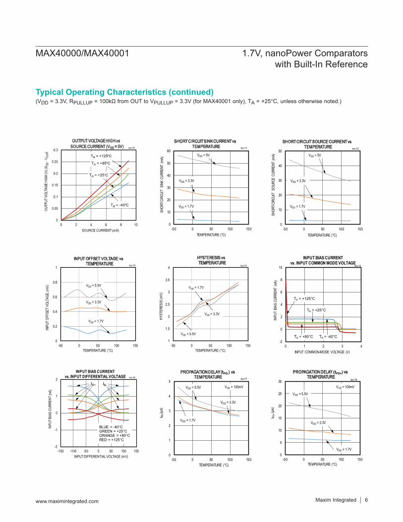
(VDD = 3.3V, RPULLUP = 100kΩ from OUT to VPULLUP = 3.3V (for MAX40001 only), TA = +25°C, unless otherwise noted.)
0
0.2
0.4
0.6
0.8
1
-50 0 50 100 150
INPU
TO
FFSE
TVO
LTAG
E(m
V)
TEMPERATURE (°C)
toc13
VDD = 5.5V
VDD = 1.7V
VDD = 3.3V
0
10
20
30
40
50
60
-50 0 50 100 150
SHO
RT-C
IRCU
ITSI
NKCU
RREN
T(m
A)
TEMPERATURE (°C)
toc11
VDD = 5V
VDD = 1.7V
VDD = 3.3V
0
10
20
30
40
50
-50 0 50 100 150
SHO
RT-C
IRCU
ITSO
URCE
CURR
ENT
(mA)
TEMPERATURE (°C)
toc12
VDD = 5V
VDD = 1.7V
VDD = 3.3V
1
1.5
2
2.5
3
3.5
4
-50 0 50 100 150
HYS
TERE
SIS
(mV)
TEMPERATURE (°C)
toc14
VDD = 5.5V
VDD = 1.7V
VDD = 3.3V
-2
0
2
4
6
8
10
0 1 2 3 4
INPU
T BI
AS C
URRE
NT (
nA)
INPUT COMMON-MODE VOLTAGE (V)
INPUT BIAS CURRENTvs. INPUT COMMON MODE VOLTAGE
toc15
TA = +125°C
TA = -40°CTA = +85°C
TA = +25°C
-2
-1
0
1
2
-150 -100 -50 0 50 100 150
INPU
T BI
AS C
UR
REN
T (n
A)
INPUT DIFFERENTIAL VOLTAGE (mV)
INPUT BIAS CURRENTvs. INPUT DIFFERENTIAL VOLTAGE toc16
IB+ IB-
BLUE = -40°CGREEN = +25°CORANGE = +85°CRED = +125°C
0
1
2
3
4
5
-50 0 50 100 150
t PD(µ
s)
TEMPERATURE (°C)
tPD-
toc17
VDD = 5.5V
VDD = 1.7V
VDD = 3.3V
VOD = 100mV
0
5
10
15
20
25
30
-50 0 50 100 150
t PD+
(µs)
TEMPERATURE (°C)
tPD+
toc18
VDD = 5.5V
VDD = 1.7V
VDD = 3.3V
VOD = 100mV
Maxim Integrated 6www.maximintegrated.com
MAX40000/MAX40001 1.7V, nanoPower Comparators with Built-In Reference
Typical Operating Characteristics (continued)

(VDD = 3.3V, RPULLUP = 100kΩ from OUT to VPULLUP = 3.3V (for MAX40001 only), TA = +25°C, unless otherwise noted.)
0
5
10
15
20
25
30
0 40 80 120 160 200
t PD+
(µs)
OVERDRIVE VOLTAGE (mV)
tPD+toc22
VDD = 3.3V
VDD = 1.7V
VDD = 5.5V
0
1
2
3
4
5
6
0 5 10 15 20 25
t PD
(µs)
CAPACITIVE LOAD (nF)
tPD-toc19
VDD = 5.5V
VDD = 1.7V
VDD = 3.3V
VOD = 100mV
1kHz FREQUENCY RESPONSE(VDD = 3.3V)
200μs/div
(2V/div)VOUT
VIN
(50mV/div)
toc24
0
5
10
15
20
25
30
0 5 10 15 20 25
t PD+
(µs)
CAPACITIVE LOAD (nF)
tPD+toc20
VDD = 5.5V
VDD = 1.7V
VDD = 3.3V
VOD = 100mV
0
4
8
12
16
0 40 80 120 160 200
t PD-(
µs)
OVERDRIVE VOLTAGE (mV)
tPD-toc21
VDD = 5.5V
VDD = 1.7V
VDD = 3.3V
10kHz FREQUENCY RESPONSE(VDD = 3.3V)
20μs/div
(2V/div)VOUT
VIN
(50mV/div)
toc25
4μs/div
(2V/div)VOUT
IN+
(50mV/div)
PROPAGATION DELAY_tPD+ (VDD = 3.3V) toc23a
4μs/div
(2V/div)VOUT
IN+
(50mV/div)
toc23b
PROPAGATION DELAY_tPD- (VDD = 3.3V)
Maxim Integrated 7www.maximintegrated.com
MAX40000/MAX40001 1.7V, nanoPower Comparators with Built-In Reference
Typical Operating Characteristics (continued)
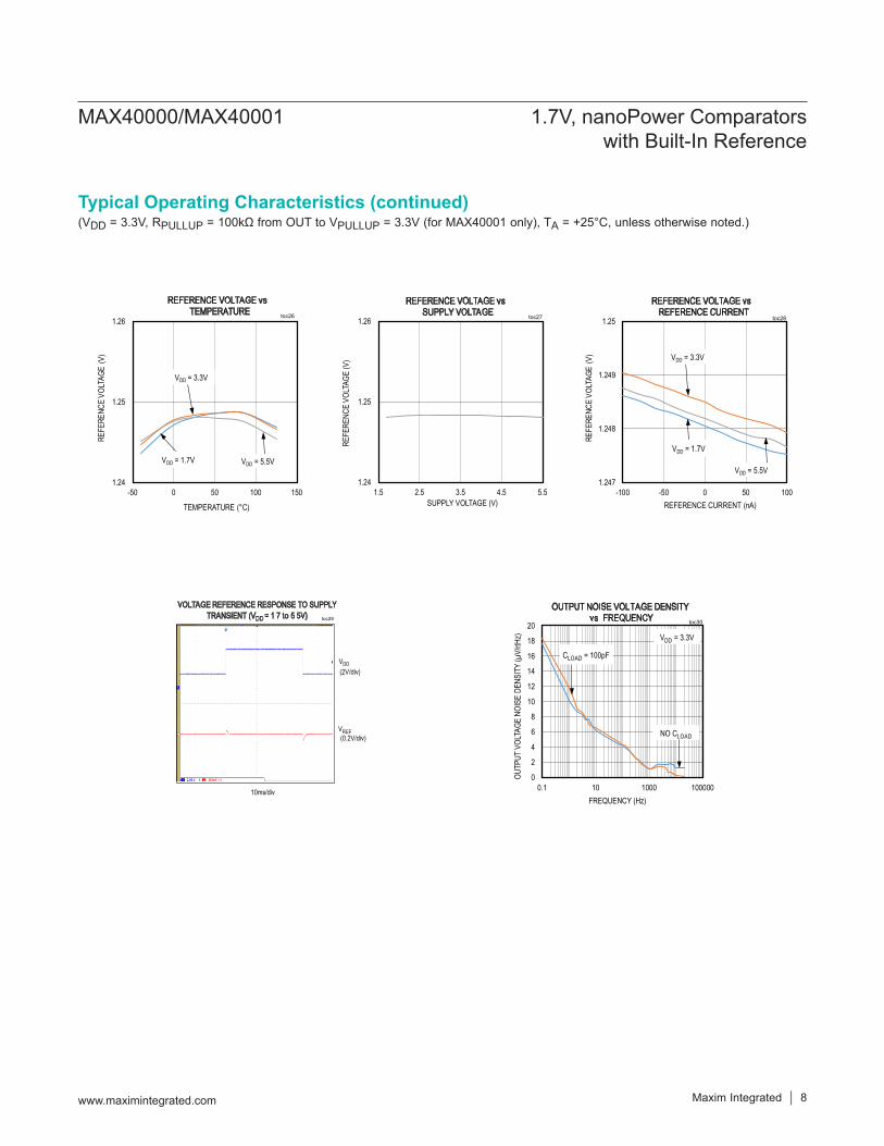
(VDD = 3.3V, RPULLUP = 100kΩ from OUT to VPULLUP = 3.3V (for MAX40001 only), TA = +25°C, unless otherwise noted.)
1.24
1.25
1.26
-50 0 50 100 150
REFE
REN
CE
VO
LTAG
E(V
)
TEMPERATURE (°C)
toc26
VDD = 5.5VVDD = 1.7V
VDD = 3.3V
1.24
1.25
1.26
1.5 2.5 3.5 4.5 5.5
REF
EREN
CE
VOLT
AGE
(V)
SUPPLY VOLTAGE (V)
toc27
1.247
1.248
1.249
1.25
-100 -50 0 50 100
REFE
REN
CE
VO
LTAG
E(V
)
REFERENCE CURRENT (nA)
toc28
VDD = 5.5V
VDD = 1.7V
VDD = 3.3V
10ms/div
(0.2V/div)VREF
(2V/div)
toc29
VDD
0
2
4
6
8
10
12
14
16
18
20
0.1 10 1000 100000
OU
TPU
TVO
LTAG
EN
OIS
ED
ENSI
TY(µ
V/rtH
z)
FREQUENCY (Hz)
toc30
NO CLOAD
CLOAD = 100pF
VDD = 3.3V
Maxim Integrated 8www.maximintegrated.com
MAX40000/MAX40001 1.7V, nanoPower Comparators with Built-In Reference
Typical Operating Characteristics (continued)

BUMP (WLP)
PIN (SOT23) NAME FUNCTION
B1 1 IM Inverting Input of Comparator
B2 3 REF Internal Voltage Reference Output. Bypass REF pin with a 0.1µF capacitor to GND as close as possible to the device.
B3 2 GND Ground
A1 6 IP Noninverting Input of Comparator
A2 5 VDDVDD Supply Voltage. Bypass VDD with a 0.1µF capacitor to GND as close as possible to the device pin.
A3 4 OUT Open-Drain Output (MAX40001)/Push-Pull Output (MAX40000). For the open-drain version, connect a 100kΩ pullup resistor from OUT to any pullup voltage up to 5.5V.
1 2 3
+A
B
MAX40000MAX40001
IP VDD OUT
GNDREFIM
TOP VIEW(BUMPS ON BOTTOM)
WLP
MAX40000/MAX40001 1.7V, nanoPower Comparators with Built-In Reference
www.maximintegrated.com Maxim Integrated 9
Pin Configurations
Pin Description
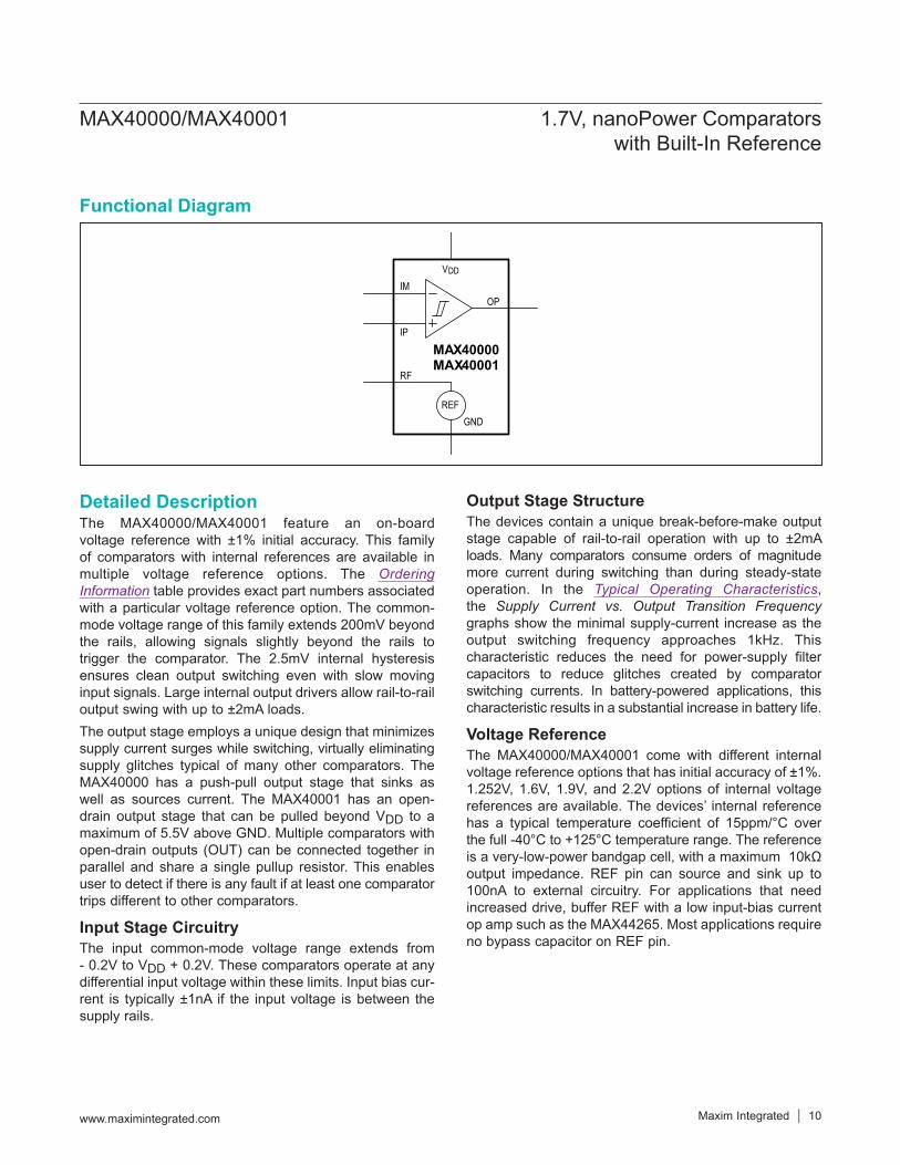
Detailed DescriptionThe MAX40000/MAX40001 feature an on-board voltage reference with ±1% initial accuracy. This family of comparators with internal references are available in multiple voltage reference options. The Ordering Information table provides exact part numbers associated with a particular voltage reference option. The common-mode voltage range of this family extends 200mV beyond the rails, allowing signals slightly beyond the rails to trigger the comparator. The 2.5mV internal hysteresis ensures clean output switching even with slow moving input signals. Large internal output drivers allow rail-to-rail output swing with up to ±2mA loads.The output stage employs a unique design that minimizes supply current surges while switching, virtually eliminating supply glitches typical of many other comparators. The MAX40000 has a push-pull output stage that sinks as well as sources current. The MAX40001 has an open-drain output stage that can be pulled beyond VDD to a maximum of 5.5V above GND. Multiple comparators with open-drain outputs (OUT) can be connected together in parallel and share a single pullup resistor. This enables user to detect if there is any fault if at least one comparator trips different to other comparators.
Input Stage CircuitryThe input common-mode voltage range extends from - 0.2V to VDD + 0.2V. These comparators operate at any differential input voltage within these limits. Input bias cur-rent is typically ±1nA if the input voltage is between the supply rails.
Output Stage StructureThe devices contain a unique break-before-make output stage capable of rail-to-rail operation with up to ±2mA loads. Many comparators consume orders of magnitude more current during switching than during steady-state operation. In the Typical Operating Characteristics, the Supply Current vs. Output Transition Frequency graphs show the minimal supply-current increase as the output switching frequency approaches 1kHz. This characteristic reduces the need for power-supply filter capacitors to reduce glitches created by comparator switching currents. In battery-powered applications, this characteristic results in a substantial increase in battery life.
Voltage ReferenceThe MAX40000/MAX40001 come with different internal voltage reference options that has initial accuracy of ±1%. 1.252V, 1.6V, 1.9V, and 2.2V options of internal voltage references are available. The devices’ internal reference has a typical temperature coefficient of 15ppm/°C over the full -40°C to +125°C temperature range. The reference is a very-low-power bandgap cell, with a maximum 10kΩ output impedance. REF pin can source and sink up to 100nA to external circuitry. For applications that need increased drive, buffer REF with a low input-bias current op amp such as the MAX44265. Most applications require no bypass capacitor on REF pin.
MAX40000MAX40001
RF
GND
IP
OP
IM
VDD
REF
MAX40000/MAX40001 1.7V, nanoPower Comparators with Built-In Reference
www.maximintegrated.com Maxim Integrated 10
Functional Diagram
Applications InformationBattery-Powered OperationThe MAX40000 and MAX40001 are ideally suited for use with most battery-powered systems. Table 1 lists Alkaline and Lithium-Ion batteries with capacities and approximate operating times for MAX40000 and MAX40001, assuming nominal conditions.
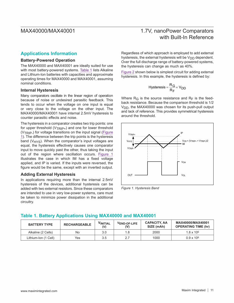
Internal HysteresisMany comparators oscillate in the linear region of operation because of noise or undesired parasitic feedback. This tends to occur when the voltage on one input is equal or very close to the voltage on the other input. The MAX40000/MAX40001 have internal 2.5mV hysteresis to counter parasitic effects and noise.The hysteresis in a comparator creates two trip points: one for upper threshold (VTRIP+) and one for lower threshold (VTRIP-) for voltage transitions on the input signal (Figure 1). The difference between the trip points is the hysteresis band (VHYS). When the comparator’s input voltages are equal, the hysteresis effectively causes one comparator input to move quickly past the other, thus taking the input out of the region where oscillation occurs. Figure 1 illustrates the case in which IM has a fixed voltage applied, and IP is varied. If the inputs were reversed, the figure would be the same, except with an inverted output.
Adding External HysteresisIn applications requiring more than the internal 2.5mV hysteresis of the devices, additional hysteresis can be added with two external resistors. Since these comparators are intended to use in very low-power systems, care must be taken to minimize power dissipation in the additional circuitry.
Regardless of which approach is employed to add external hysteresis, the external hysteresis will be VDD dependent. Over the full discharge range of battery-powered systems, the hysteresis can change as much as 40%.Figure 2 shown below is simplest circuit for adding external hysteresis. In this example, the hysteresis is defined by:
GDD
F
RHysteresis VR
= ×
Where RG is the source resistance and RF is the feed-back resistance. Because the comparison threshold is 1/2 VDD, the MAX40000 was chosen for its push-pull output and lack of reference. This provides symmetrical hysteresis around the threshold.
Figure 1. Hysteresis Band
Table 1. Battery Applications Using MAX40000 and MAX40001
BATTERY TYPE RECHARGEABLE VINITIAL (V)
VEND-OF-LIFE (V)
CAPACITY, AA SIZE (mAh)
MAX40000/MAX40001OPERATING TIME (hr)
Alkaline (2 Cells) No 3.0 1.8 2000 1.8 x 10⁶
Lithium-Ion (1 Cell) Yes 3.5 2.7 1000 0.9 x 10⁶
IP
IMVOS = (VTRIP+ + VTRIP-)/2
VTRIP+
VTRIP-
VHYS
VOH
VOLOUT
MAX40000/MAX40001 1.7V, nanoPower Comparators with Built-In Reference
www.maximintegrated.com Maxim Integrated 11

Output ConsiderationsIn most cases, the push-pull output of MAX40000 is best for external hysteresis. The open-drain output of the MAX40001 can be used, but the effect of the feedback network and pullup resistor on the actual output high voltage must be considered.
Component SelectionBecause the MAX40000/MAX40001 are intended for very low power-supply systems, the highest impedance circuits should be used wherever possible. The offset error due to input-bias current is proportional to the total impedance seen at the input. For example, selecting components for Figure 2, with a target of 50mV hysteresis, a 5V supply, and choosing an RF of 10MΩ gives RG as 100kΩ. The total impedance seen at IN+ is therefore 10MΩ || 100kΩ, or 99kΩ. The maximum Input bias current of MAX40000/MAX40001 is 1nA; therefore, the error due to source impedance is less than 100μV.
Board Layout and BypassingPower-supply bypass capacitors are not typically needed, but use 100nF bypass capacitors close to the device’s supply pins when supply impedance is high, supply leads are long, or excessive noise is expected on the sup-ply lines. Minimize signal trace lengths to reduce stray
capacitance. A ground plane and surface-mount components are recommended. If the REF pin is decoupled, use a new low-leakage capacitor.
Logic-Level TranslatorThe Typical Application Circuit shows an application that converts 5V logic to 3V logic levels. The MAX40001 is powered by the +5V supply voltage to VDD, and the pullup resistor for the MAX40001’s open-drain output is connected to the +3V supply voltage. This configuration allows the full 5V logic swing without creating overvoltage on the 3V logic inputs. For 3V to 5V logic-level translations, simply connect the +3V supply voltage to VDD and the +5V supply voltage to the pullup resistor.
Figure 2. External Hysteresis on MAX40000
VDD
VDD/2
MAX40000
VIN+
RG RF
IPOUT
IM
VDD
GND
MAX40001VPULL = 3V
1.7V TO 5.5V
5V (3V) LOGIC IN
100kΩ
100kΩ
100kΩ
MAX40000/MAX40001 1.7V, nanoPower Comparators with Built-In Reference
www.maximintegrated.com Maxim Integrated 12
Typical Application Circuit

+Denotes a lead (Pb)-free/RoHS-compliant package.T = Tape and reel.For example, the MAX40000ANT12+T has an onboard 1.2V reference voltage.Devices without “_ _” use external reference voltage as supply voltage.*Future product—contact factory for availability.
PART TEMP RANGE PIN- PACKAGE
TOP MARK
MAX40000ANT12+T -40°C to +125°C 6 WLP +NMAX40000ANT16+T* -40°C to +125°C 6 WLP +OMAX40000ANT19+T* -40°C to +125°C 6 WLP +PMAX40000ANT22+T* -40°C to +125°C 6 WLP +QMAX40000AUT12+T -40°C to +125°C 6 SOT23 –MAX40000AUT16+T* -40°C to +125°C 6 SOT23 –MAX40000AUT19+T* -40°C to +125°C 6 SOT23 –MAX40000AUT22+T* -40°C to +125°C 6 SOT23 –MAX40001ANT12+T -40°C to +125°C 6 WLP +RMAX40001ANT16+T* -40°C to +125°C 6 WLP +SMAX40001ANT19+T* -40°C to +125°C 6 WLP +TMAX40001ANT22+T -40°C to +125°C 6 WLP +UMAX40001AUT12+T -40°C to +125°C 6 SOT23 –MAX40001AUT16+T* -40°C to +125°C 6 SOT23 –MAX40001AUT19+T* -40°C to +125°C 6 SOT23 –MAX40001AUT22+T -40°C to +125°C 6 SOT23 –
PACKAGE TYPE
PACKAGECODE
OUTLINE NO.
LAND PATTERN NO.
6 WLP N60D1+1 21-100086 Refer to Application Note 1891
6 SOT23 U6+1 21-0058 90-0175
MAX40000/MAX40001 1.7V, nanoPower Comparators with Built-In Reference
www.maximintegrated.com Maxim Integrated 13
Chip InformationPROCESS: BiCMOS
Ordering Information
Package InformationFor the latest package outline information and land patterns (footprints), go to www.maximintegrated.com/packages. Note that a “+”, “#”, or “-” in the package code indicates RoHS status only. Package drawings may show a different suffix character, but the drawing pertains to the package regardless of RoHS status.

REVISIONNUMBER
REVISIONDATE DESCRIPTION PAGES
CHANGED
0 1/17 Initial release —
1 3/17 Updated title to include “nanoPower” 1–14
2 4/17 Updated Ordering Information table 13
3 5/17 Updated Ordering Information table 13
4 8/17 Updated Functional Diagram and Ordering Information table 10, 13
Maxim Integrated cannot assume responsibility for use of any circuitry other than circuitry entirely embodied in a Maxim Integrated product. No circuit patent licenses are implied. Maxim Integrated reserves the right to change the circuitry and specifications without notice at any time. The parametric values (min and max limits) shown in the Electrical Characteristics table are guaranteed. Other parametric values quoted in this data sheet are provided for guidance.
Maxim Integrated and the Maxim Integrated logo are trademarks of Maxim Integrated Products, Inc. © 2017 Maxim Integrated Products, Inc. 14
MAX40000/MAX40001 1.7V, nanoPower Comparators with Built-In Reference
Revision History
For pricing, delivery, and ordering information, please contact Maxim Direct at 1-888-629-4642, or visit Maxim Integrated’s website at www.maximintegrated.com.