max2990 integrated power-line digital … · max2990 programming manual rev 1.4 . maxim integrated...
TRANSCRIPT
Maxim Integrated - 1 -
MAX2990 INTEGRATED POWER-LINE DIGITAL TRANSCEIVER
PROGRAMMING MANUAL
MAX2990 Programming Manual Rev 1.4
Maxim Integrated - 2 -
TABLE OF CONTENTS
MAX2990 Functional Description ...................................................................................... 4
Buffer Manager:............................................................................................................................... 4
Data Manager:................................................................................................................................ 4
CRC/DES: .................................................................................................................................. 5
MCU SPR Registers:....................................................................................................................... 5
MCU SFR Registers:....................................................................................................................... 5
Flash, Util. ROM, Data SRAM and MMU:..................................................................................... 5
JTAG/EMM:............................................................................................................................... 6
CLKGEN:.................................................................................................................................... 6
MAXQ Core: ................................................................................................................................ 6
MAXQ Peripherals: ........................................................................................................................ 6
MAXQ MCU .............................................................................................................................. 6
Special Purpose Registers: .................................................................................................................. 6
Special Function Registers: ............................................................................................................... 21
UART (Universal Asynchronous Receiver/Transmitter)......................................... 58
UART SFRs............................................................................................................................... 59
UART Operating Modes ................................................................................................................ 61
UART Baud Rate Generation......................................................................................................... 63
Timer B ...................................................................................................................................... 63
GPIO........................................................................................................................................... 64
I/O Port Description...................................................................................................................... 64
The Test Access (JTAG) Port ............................................................................................ 66
PHY Frame Format ............................................................................................................... 66
MAC Code ................................................................................................................................ 68
Changing Transmitter Gain ............................................................................................................. 68
Changing Modulation Scheme and Communication Standard ................................................................. 69
MAC functions description .............................................................................................................. 70 Main function example flowchart ................................................................................................... 70

MAX2990 Programming Manual Rev 1.4
Maxim Integrated - 3 -
System Init ................................................................................................................................ 70 Interrupt................................................................................................................................... 74 LED ........................................................................................................................................ 76 Timer....................................................................................................................................... 76 Encryption ................................................................................................................................ 77 MAC functions .......................................................................................................................... 78 PHY functions ........................................................................................................................... 80 Channel Estimation..................................................................................................................... 84 CSMA(Carrier Sense Multiple Access) ............................................................................................. 84 Miscellaneous ............................................................................................................................ 84 Macros description...................................................................................................................... 86 Global variables description .......................................................................................................... 87
MAX2990 Programming Manual Rev 1.4
Maxim Integrated - 4 -
MAX2990 Functional Description
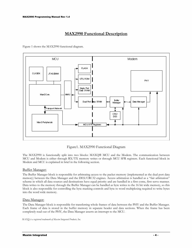
Figure 1 shows the MAX2990 functional diagram.
Figure1. MAX2990 Functional Diagram The MAX2990 is functionally split into two blocks: MAXQ® MCU and the Modem. The communication between MCU and Modem is either through RX/TX memory writes or through MCU SFR registers. Each functional block in Modem and MCU is explained in brief in the following section.
Buffer Manager: The Buffer Manager block is responsible for arbitrating access to the packet memory (implemented as the dual port data memory) between the Data Manager and the DES/CRC32 engines. Access arbitration is handled as a “fair arbitration” scheme in which all data sources and destinations have equal priority and are handled in a first come, first serve manner. Data writes to the memory through the Buffer Manager can be handled as byte writes to the 16 bit wide memory, so this block is also responsible for controlling the byte masking controls and byte to word multiplexing required to write bytes into the word wide memory.
Data Manager: The Data Manager block is responsible for transferring whole frames of data between the PHY and the Buffer Manager. Each frame of data is stored in the buffer memory in separate header and data sections. When the frame has been completely read out of the PHY, the Data Manager asserts an interrupt to the MCU.
MAXQ is a registered trademark of Maxim Integrated Products, Inc.

MAX2990 Programming Manual Rev 1.4
Maxim Integrated - 5 -
CRC/DES: The DES encryption and CRC32 functions can be enabled separately. If DES function is enabled, data is encrypted or decrypted, depending on the mode set, and written back to memory. If CRC32 is enabled, a CRC32 checksum is calculated and appended to the end of data block. If both CRC32 and DES are enabled, CRC32 checksum is calculated, encrypted and then appended to the data block.
MCU SPR Registers: MCU SPR Registers are explained in detail in MAXQ Core description.
MCU SFR Registers: MCU SFR Registers are explained in detail in MAXQ Core description.
Flash, Util. ROM, Data SRAM and MMU: Figure 2 shows the MAX2990 memory organization.
x00
x06
x0F
x07
SPRs
x0000
xFFFF xFFFF
64K Data Memory
Registers
x0000
64Kx16 ProgramMemory
SFRs
x1F
xFF
x00
x0F
16x16Stack
16Kx16Flash
x3FFF
2.5Kx16 Utility ROM
x8000
x89FF
2Kx16 SPRAM
2Kx16 DPRAM
x07FF
x1000
x17FF
Figure 2. MAX2990 Memory Organization
The MAX2990 has 32KB of flash memory, 5KB of Utility ROM for system startup and programming routines, test support routines and miscellaneous non-volatile data that is not used for system configuration (such as the boot loader access password). There are two data memories, 4KB Single Port Data SRAM and 128KB of Dual Port Data SRAM.
MAX2990 Programming Manual Rev 1.4
Maxim Integrated - 6 -
Memory Management Unit (MMU) provides memory allocation and access control to program and data memories.
JTAG/EMM: JTAG is a debug/programming port for MAXQ MCU. JTAG interface is discussed in detail in MAXQ MCU core section.
CLKGEN: CLKGEN is a functional block, which generates system clock from external clock source (oscillator or resonator) or an internal oscillator circuit.
MAXQ Core: MAXQ is a low-power 16-bit RISC processor based on Harvard Memory Architecture. It has 16-bit program memory bus and all instructions are 16 bits in length. The registers and the peripherals are explained in detail in MAXQ MCU section.
MAXQ Peripherals: MAXQ MCU has seven 16-bit timers, UART, 4-wire SPI™, I2C, and Real Time Clock (RTC). Each peripheral description is in the MAXQ MCU section.
MAXQ MCU
Special Purpose Registers:
Register Description AP (00h, 08h)
Initialization:
Read/Write Access:
AP.3 – AP.0
AP.7 – AP.4
Accumulator Pointer (8-bit register)
This register is cleared to 00h on all forms of reset.
Unrestricted direct Read/Write.
Active Accumulator select bits. The setting of these bits activates one of the 8/16 Accumulators
in the Accumulator module (A) to function as the Active Accumulator for arithmetic and logical
operations. The setting of the these bits can be automatically incremented/decremented in a
modulo fashion according to the setting to the APC register.
(Bit 3 is reserved and is tried to 0 for Implementation with 8 accumulators)
Reserved, read returns 0.
SPI is a trademark of Motorola, Inc.

MAX2990 Programming Manual Rev 1.4
Maxim Integrated - 7 -
Register Description APC (01h, 08h)
Initialization:
Read/Write Access:
APC.0: MOD0
APC.1: MOD1
APC.2: MOD2
APC.5 – APC.3
APC.6: IDS
APC.7: CLR
Accumulator Pointer Control (8-bit register)
This register is cleared to 00h on all forms of reset.
Unrestricted direct Read/Write.
Modulo Bit 0
Modulo Bit 1
Modulo Bit 2
The Accumulator Pointer Auto-Increment/Decrement function will be activate when these
bits are set to value other then 000b. The modulo is selected accordingly when Active
Pointer Auto-Increment/Decrement is active:
MOD2,MOD1,MOD0 Modulo
000 Default, no AP auto-increment/decrement
001 Modulo 2
010 Modulo 4
011 Modulo 8
100 Modulo 16 (not valid for 8 accumulators, MOD2 is tied to 0)
101 – 111 Reserved (for 16 accumulators modulo 16 if set; MOD2 is tied
0 for 8-accumulator implementation).
Note the MOVE AP, Acc instruction (880Ah) causing AP auto-Inc/Dec will happen if enabled, no
data transfer will perform.
Reserved, read returns 0.
Increment/Decrement Select. When this bit is cleared to 0, the content of AP will be
increment after an arithmetic or logical operation, When this bit is set to 1, the content of
AP will be decremented after an arithmetic or logical operation.
AP Clear. When this bit is set to 1, the content of AP will be cleared to 0. This bit will be
automatically reset to 0 after clearing the AP register. Note if the MOVE APC, Acc instruction
(980Ah) causes the CLR bit to set, the clear operation will override other functions, i.e. the AP
auto-Inc/Dec will not happen.

MAX2990 Programming Manual Rev 1.4
Maxim Integrated - 8 -
Register Description PSF (04h, 08h)
Initialization:
Read/Write Access:
PSF.0: E
PSF.1: C
PSF.2: OV
PSF.3: GPF0
PSF.4: GPF1
PSF.5
PSF.6: S
PSF.7: Z
Processor Status Flags Register (8-bit register)
This register is cleared to x80h on all forms of reset.
Unrestricted direct Read. Write access to OV, E, C, GPF1 and GPF0 bits only.
Equal Flag. This flag reflects the state of Equal bit of a compare operation. It will be 1
when the two values are equal. It will be 0 when the two values are different. Write a 1 to
this bit by software is effectively set the Equal flag.
Carry Flag. This flag reflects the state of Carry bit of the active Accumulator. Its state
may change after an arithmetic and logical operation. This flag is set to 1 if the last
operation resulted in a carry/borrow. Otherwise it is cleared to 0. Write a 1 to this bit by
software is effectively set the Carry flag.
Overflow Flag. This flag is set to 1 if there is a carry out of bit 14 but not out of bit 15, or a carry
out of bit 15 bit not out of bit 14 from the last arithmetic operation, otherwise, the OV is remained
as 0. When adding signed numbers, OV indicates a negative number resulted as the sum of two
positive operands, or a positive sum resulted from two negative operands. For subtraction, OV is
set if a borrow is needed into bit 14 but not into bit 15, or into bit 15 but not into bit 14. This bit is
read and write to the CPU to allow it to be restored after events such as interrupt servicing and
debug operations.
General-Purpose Flag 0. This is a general-purpose flag for software control.
General-Purpose Flag 1. This is a general-purpose flag for software control.
Reserved, read returns 0
Sign Flag. This flag reflects the state of Sign bit of the active Accumulator (the most
significant bit of the active Accumulator). Its state may change after an arithmetic and
logical operation or after switch of active Accumulator. When it is set to 1, it indicates a
negative value in the active Accumulator from the last operation. When it is cleared to 0, it
indicates a positive value. This is a read only bit.
Zero Flag. This flag reflects the state of Zero bit of the active Accumulator (bit-wise NOR
of the active Accumulator). Its state may change after an arithmetic and logical operation
or after switch of active Accumulator. When it is set to 1, it indicates a zero value as result
of the last operation. When it is cleared to 0, it indicates a non-zero value. This is a read only bit.
IC (05h, 08h)
Initialization:
Read/Write Access:
IC.0: IGE
IC.1: INS
IC.4 – IC.2
IC.5: CGDS
IC.7 – IC.6
Interrupt and Control Register (8-bit register)
This register is cleared to 00h on all forms of reset.
Unrestricted direct Read/Write.
Interrupt Global Enable The IGE bit enables the interrupt handler if set to 1. No
interrupt to the CPU is allowed if this bit is cleared to 0.
Interrupt In Service. The INS will be set by the interrupt handler automatically when an
interrupt is acknowledged. No further interrupt will occur as long as the INS remains set. The
interrupt service routine can clear the INS to allow interrupt nesting. Otherwise, execution of an
RETI/POPI instruction the INS will be cleared automatically by the interrupt handler.
Reserved, read returns 0.
System Clock Gating Disable. The system clock gating circuitry is disabled if the CGDS
bit is set to 1. When this bit is cleared, the system clock gating circuitry is activated.
Reserved, read returns 0.

MAX2990 Programming Manual Rev 1.4
Maxim Integrated - 9 -
Register Description IMR (06h, 08h)
Initialization:
Read/Write Access:
IMR.0: IM0
IMR.1: IM1
IMR.2: IM2
IMR.3: IM3
IMR.4: IM4
IMR.5: IM5
IMR.6:
IMR.7: IMS
Interrupt Mask Register (8-bit register)
This register is 00h on all forms of reset.
Unrestricted direct Read/Write
Interrupt Mask 0. This bit is the module level interrupt enable for register module 0. To
activate the interrupt request from module 0, the IGE and IM0 must be set and the INS is not set.
Clearing this bit to 0 disables all interrupt sources in module 0.
Interrupt Mask 1. This bit is the module level interrupt enable for register module 1. To
activate the interrupt request from module 1, the IGE and IM01 must be set and the INS is not set.
Clearing this bit to 0 disables all interrupt sources in module 1.
Interrupt Mask 2. This bit is the module level interrupt enable for register module 2. To
activate the interrupt request from module 2, the IGE and IM2 must be set and the INS is not set.
Clearing this bit to 0 disables all interrupt sources in module 2.
Interrupt Mask 3. This bit is the module level interrupt enable for register module 3. To
activate the interrupt request from module 3, the IGE and IM3 must be set and the INS is not set.
Clearing this bit to 0 disables all interrupt sources in module 3.
Interrupt Mask 4. This bit is the module level interrupt enable for register module 4. To
activate the interrupt request from module 4, the IGE and IM4 must be set and the INS is not set.
Clearing this bit to 0 disables all interrupt sources in module 4.
Interrupt Mask 5. This bit is the module level interrupt enable for register module 5. To
activate the interrupt request from module 5, the IGE and IM5 must be set and the INS is not set.
Clearing this bit to 0 disables all interrupt sources in module 5.
Reserved, read returns 0.
Interrupt Mask System. This bit is the module level interrupt enable for SPR modules. To
activate the interrupt request from any SPR modules, the IGE and IMS must be set and the INS is
not set. Clearing this bit to 0 disables all interrupt sources in all SPR modules.

MAX2990 Programming Manual Rev 1.4
Maxim Integrated - 10 -
Register Description SC (08h, 08h)
Initialization:
Read/Write Access:
SC.0:
SC.1: PWL
SC.2: ROD
SC.3: UPA
SC.4: CDA0
SC.5: CDA1
SC.6
SC.7:TAP
System Control Register (8-bit register)
This register is 100000s0b on all forms of reset. Bit 1 (PWL) is set by power-on reset only
Unrestricted direct Read/Write.
Reserved, read returns 0.
Password Lock. This bit defaults to 1 on a power-on reset. When this bit is 1, it requires a 32-
byte password to be matched with the password in the program space before allowing access to
the ROM Loader’s utilities for read/write of program memory and debug functions. Clearing this
bit to 0 disables the password protection to the ROM Loader.
ROM Operation Done. This bit is used to signify completion of a ROM operation sequence to
the control units. This allows the Debug engine to determine the status of a ROM sequence.
Setting this bit to logic 1 causes an internal system reset if the SPE bit is also set. Setting the ROD
bit will clear the SPE bit if it is set and the ROD bit will be automatically cleared by hardware
once the control unit acknowledged the done indication.
Upper Program Access. The physical program memory is logically divided into four pages; P0
and P1 occupy the lower 32K words while P2 and P3 occupy the upper 32K words. P0 and P1 are
assigned to the lower half of the program space and is always active. However, P2 and P3 must be
implicitly activated in the upper half of the program space by setting the UPA bit to logic 1 for
normal program execution. When UPA bit is cleared to 0, the upper program memory space is
occupied by the Utility ROM and the physical data to be accessible as program memory.
Note that the UPA is not implemented if the upper 32K of the program space is not used for the
user code.
Code Data Access Bit 0.
Code Data Access Bit 1.
The CDA bits are used to logically map physical program memory page to the data space for
read/write access:
CDA1 CDA0 Byte Mode Active Page Word Mode Active Page
0 0 P0 P0 and P1
0 1 P1 P0 and P1
1 0 P2 P2 and P3
1 1 P3 P2 and P3
The logical addresses are depending on which memory segment is executing. Note that CDA1 is
not implemented if the upper 32K of the program space is not used for the user code. No CDA
bits are needed if only one page program space is incorporated.
Reserved, read returns 0.
Test Access (JTAG) Port Enable. This bit controls whether the Test Access Port special
function pins are enabled. The TAP defaults to being enabled. Clearing this bit to a logic ‘0’ will
disable the TAP special function on the JTAG pins.

MAX2990 Programming Manual Rev 1.4
Maxim Integrated - 11 -
Register Description IIR (0Bh, 08h)
Initialization:
Read/Write Access:
IIR.0: II0
IIR.1: II1
IIR.2: II2
IIR.3: II3
IIR.4: II4
IIR.5: II5
IIR.6:
IIR.7: IIS
Interrupt Identification Register (8-bit register)
This register is 00h on all forms of reset.
Unrestricted direct Read. Write access is a no-operation.
Interrupt ID 0. When this bit is set to 1, it indicates that there is at least one pending
interrupt in register module 0. This bit is set only if the interrupt flag and its corresponding
enable bit are set. The II0 is cleared by hardware when the interrupt source is disabled or
the flag is cleared by software.
Interrupt ID 1. When this bit is set to 1, it indicates that there is at least one pending
interrupt in register module 1. This bit is set only if the interrupt flag and its corresponding
enable bit are set. The II1 is cleared by hardware when the interrupt source is disabled or
the flag is cleared by software
Interrupt ID 2. When this bit is set to 1, it indicates that there is at least one pending
interrupt in register module 2. This bit is set only if the interrupt flag and its corresponding
enable bit are set. The II2 is cleared by hardware when the interrupt source is disabled or
the flag is cleared by software
Interrupt ID 3. When this bit is set to 1, it indicates that there is at least one pending
interrupt in register module 3. This bit is set only if the interrupt flag and its corresponding
enable bit are set. The II3 is cleared by hardware when the interrupt source is disabled or
the flag is cleared by software
Interrupt ID 4. When this bit is set to 1, it indicates that there is at least one pending
interrupt in register module 4. This bit is set only if the interrupt flag and its corresponding
enable bit are set. The II4 is cleared by hardware when the interrupt source is disabled or
the flag is cleared by software.
Interrupt ID 5. When this bit is set to 1, it indicates that there is at least one pending
interrupt in register module 5. This bit is set only if the interrupt flag and its corresponding
enable bit are set. The II5 is cleared by hardware when the interrupt source is disabled or
the flag is cleared by software.
Reserved, read returns 0.
Interrupt ID System. When this bit is set to 1, it indicates that there is at least one pending
interrupt in SPR modules. This bit is set only if the interrupt flag and its corresponding
enable bit are set. The IIS is cleared by hardware when the interrupt source is disabled
or the flag is cleared by software.
MAX2990 Programming Manual Rev 1.4
Maxim Integrated - 12 -
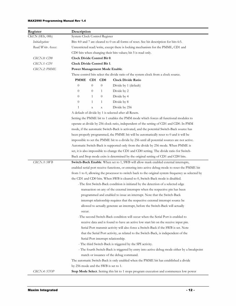
Register Description CKCN (0Eh, 08h)
Initialization:
Read/Write Access:
CKCN.0: CD0
CKCN.1: CD1
CKCN.2: PMME
System Clock Control Register
Bits 4:0 and 7 are cleared to 0 on all forms of reset. See bit description for bits 6:5.
Unrestricted read/write, except there is locking mechanism for the PMME, CD1 and
CD0 bits when changing their bits values; bit 5 is read only.
Clock Divide Control Bit 0.
Clock Divide Control Bit 1.
Power Management Mode Enable.
These control bits select the divide ratio of the system clock from a clock source.
PMME CD1 CD0 Clock Divide Ratio
0 0 0 Divide by 1 (default)
0 0 1 Divide by 2
0 1 0 Divide by 4
0 1 1 Divide by 8
1 x x Divide by 256
A default of divide by 1 is selected after all Resets.
Setting the PMME bit to 1 enables the PMM mode which forces all functional modules to
operate at divide by 256 clock ratio, independent of the setting of CD1 and CD0. In PMM
mode, if the automatic Switch-Back is activated, and the potential Switch-Back source has
been properly programmed, the PMME bit will be automatically reset to 0 and it will be
impossible to set the PMME bit to a divide by 256 until all potential sources are not active.
Automatic Switch-Back is supported only from the divide by 256 mode. When PMME is
set, it is also impossible to change the CD1 and CD0 setting. The divide ratio for Switch-
Back and Stop mode exits is determined by the original setting of CD1 and CD0 bits.
CKCN.3: SWB
CKCN.4: STOP
Switch-Back Enable. When set to 1, SWB will allow mask enabled external interrupts,
enabled serial port receive functions, or entering into active debug mode to reset the PMME bit
from 1 to 0, allowing the processor to switch back to the original system frequency as selected by
the CD1 and CD0 bits. When SWB is cleared to 0, Switch-Back mode is disabled.
-The first Switch-Back condition is initiated by the detection of a selected edge
transaction on any of the external interrupts when the respective pin has been
programmed and enabled to issue an interrupt. Note that the Switch-Back
interrupt relationship requires that the respective external interrupt source be
allowed to actually generate an interrupt, before the Switch-Back will actually
occur.
-The second Switch-Back condition will occur when the Serial Port is enabled to
receive data and is found to have an active low start bit on the receive input pin.
Serial Port transmit activity will also force a Switch-Back if the SWB is set. Note
that the Serial Port activity, as related to the Switch-Back, is independent of the
Serial Port interrupt relationship.
- The third Switch-Back is triggered by the SPI activity.
- The fourth Switch-Back is triggered by entry into active debug mode either by a breakpoint
match or issuance of the debug command.
The automatic Switch-Back is only enabled when the PMME bit has established a divide
by 256 mode and the SWB is set to 1.
Stop Mode Select. Setting this bit to 1 stops program execution and commences low power

MAX2990 Programming Manual Rev 1.4
Maxim Integrated - 13 -
Register Description
CKCN.5: RGMD
CKCN.6: RGSL
CKCN.7: IDLE
operation. This bit is cleared by a reset or any of the enabled external interrupts. Setting and
resetting the STOP bit will not change the system clock source and the divide ratio.
Ring Oscillator Mode. This read only bit reflects the selection of clock source. RGMD=1
indicates the ring oscillator is providing the system clock. RGMD=0 indicates that the system
clock is being derived from the external crystal or clock.
Ring Oscillator Select. This bit selects the internal ring oscillator for system clock generation.
When RGSL is set to 1, the internal ring oscillator (following the PMME, CD1:0 selected divide
ratio) is immediately sourced as the system clock and the internal crystal amplifier and PLL are
disabled. When RGSL is cleared to 0, the internal ring oscillator (following the clock divide
selection) will continue to serve as the system clock until the crystal warm-up counter has expired
and PLL output is ready. At which point, that clock (following the PMME, CD1:0 selected divide
ratio) is sourced as the system clock. The RGSL bit is cleared to 0 on power-on reset only and is
unaffected by other resets.
IDLE Mode Select. Setting this bit to a 1 stops program execution by halting the Instruction
Pointer and disabling the internal module selects (similar to a NOP operation). This provides a
low power mode that does not require a crystal warmup on exit.
MAX2990 Programming Manual Rev 1.4
Maxim Integrated - 14 -
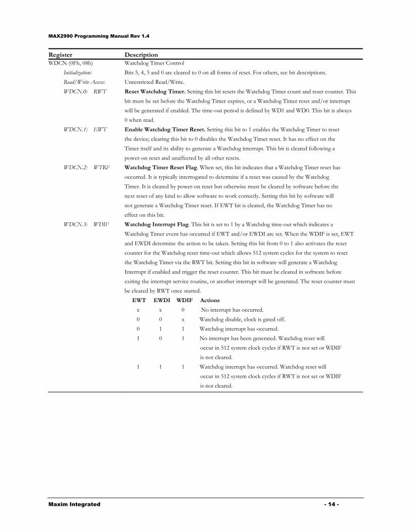
Register Description WDCN (0Fh, 08h)
Initialization:
Read/Write Access:
WDCN.0: RWT
WDCN.1: EWT
WDCN.2: WTRF
WDCN.3: WDIF
Watchdog Timer Control
Bits 5, 4, 3 and 0 are cleared to 0 on all forms of reset. For others, see bit descriptions.
Unrestricted Read/Write.
Reset Watchdog Timer. Setting this bit resets the Watchdog Timer count and reset counter. This
bit must be set before the Watchdog Timer expires, or a Watchdog Timer reset and/or interrupt
will be generated if enabled. The time-out period is defined by WD1 and WD0. This bit is always
0 when read.
Enable Watchdog Timer Reset. Setting this bit to 1 enables the Watchdog Timer to reset
the device; clearing this bit to 0 disables the Watchdog Timer reset. It has no effect on the
Timer itself and its ability to generate a Watchdog interrupt. This bit is cleared following a
power-on reset and unaffected by all other resets.
Watchdog Timer Reset Flag. When set, this bit indicates that a Watchdog Timer reset has
occurred. It is typically interrogated to determine if a reset was caused by the Watchdog
Timer. It is cleared by power-on reset but otherwise must be cleared by software before the
next reset of any kind to allow software to work correctly. Setting this bit by software will
not generate a Watchdog Timer reset. If EWT bit is cleared, the Watchdog Timer has no
effect on this bit.
Watchdog Interrupt Flag. This bit is set to 1 by a Watchdog time-out which indicates a
Watchdog Timer event has occurred if EWT and/or EWDI are set. When the WDIF is set, EWT
and EWDI determine the action to be taken. Setting this bit from 0 to 1 also activates the reset
counter for the Watchdog reset time-out which allows 512 system cycles for the system to reset
the Watchdog Timer via the RWT bit. Setting this bit in software will generate a Watchdog
Interrupt if enabled and trigger the reset counter. This bit must be cleared in software before
exiting the interrupt service routine, or another interrupt will be generated. The reset counter must
be cleared by RWT once started.
EWT EWDI WDIF Actions
x x 0 No interrupt has occurred.
0 0 x Watchdog disable, clock is gated off.
0 1 1 Watchdog interrupt has occurred.
1 0 1 No interrupt has been generated. Watchdog reset will
occur in 512 system clock cycles if RWT is not set or WDIF
is not cleared.
1 1 1 Watchdog interrupt has occurred. Watchdog reset will
occur in 512 system clock cycles if RWT is not set or WDIF
is not cleared.
MAX2990 Programming Manual Rev 1.4
Maxim Integrated - 15 -
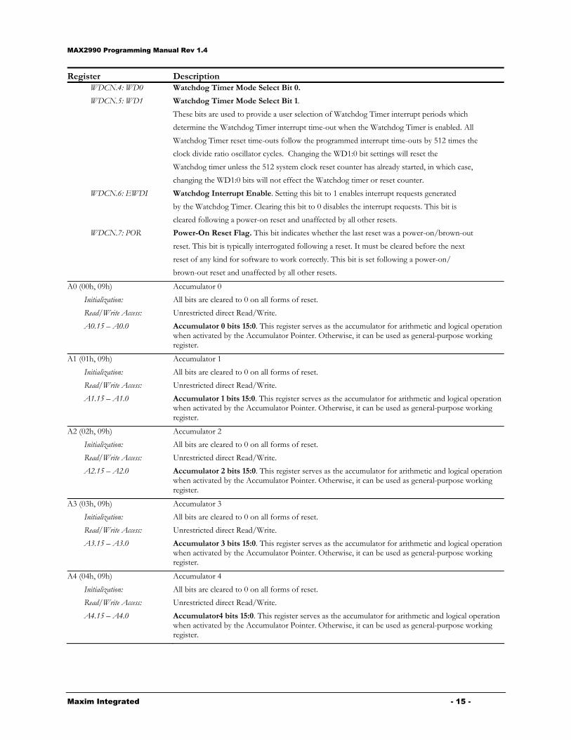
Register Description WDCN.4: WD0
WDCN.5: WD1
WDCN.6: EWDI
WDCN.7: POR
Watchdog Timer Mode Select Bit 0.
Watchdog Timer Mode Select Bit 1.
These bits are used to provide a user selection of Watchdog Timer interrupt periods which
determine the Watchdog Timer interrupt time-out when the Watchdog Timer is enabled. All
Watchdog Timer reset time-outs follow the programmed interrupt time-outs by 512 times the
clock divide ratio oscillator cycles. Changing the WD1:0 bit settings will reset the
Watchdog timer unless the 512 system clock reset counter has already started, in which case,
changing the WD1:0 bits will not effect the Watchdog timer or reset counter.
Watchdog Interrupt Enable. Setting this bit to 1 enables interrupt requests generated
by the Watchdog Timer. Clearing this bit to 0 disables the interrupt requests. This bit is
cleared following a power-on reset and unaffected by all other resets.
Power-On Reset Flag. This bit indicates whether the last reset was a power-on/brown-out
reset. This bit is typically interrogated following a reset. It must be cleared before the next
reset of any kind for software to work correctly. This bit is set following a power-on/
brown-out reset and unaffected by all other resets.
A0 (00h, 09h)
Initialization:
Read/Write Access:
A0.15 – A0.0
Accumulator 0
All bits are cleared to 0 on all forms of reset.
Unrestricted direct Read/Write.
Accumulator 0 bits 15:0. This register serves as the accumulator for arithmetic and logical operation when activated by the Accumulator Pointer. Otherwise, it can be used as general-purpose working register.
A1 (01h, 09h)
Initialization:
Read/Write Access:
A1.15 – A1.0
Accumulator 1
All bits are cleared to 0 on all forms of reset.
Unrestricted direct Read/Write.
Accumulator 1 bits 15:0. This register serves as the accumulator for arithmetic and logical operation when activated by the Accumulator Pointer. Otherwise, it can be used as general-purpose working register.
A2 (02h, 09h)
Initialization:
Read/Write Access:
A2.15 – A2.0
Accumulator 2
All bits are cleared to 0 on all forms of reset.
Unrestricted direct Read/Write.
Accumulator 2 bits 15:0. This register serves as the accumulator for arithmetic and logical operation when activated by the Accumulator Pointer. Otherwise, it can be used as general-purpose working register.
A3 (03h, 09h)
Initialization:
Read/Write Access:
A3.15 – A3.0
Accumulator 3
All bits are cleared to 0 on all forms of reset.
Unrestricted direct Read/Write.
Accumulator 3 bits 15:0. This register serves as the accumulator for arithmetic and logical operation when activated by the Accumulator Pointer. Otherwise, it can be used as general-purpose working register.
A4 (04h, 09h)
Initialization:
Read/Write Access:
A4.15 – A4.0
Accumulator 4
All bits are cleared to 0 on all forms of reset.
Unrestricted direct Read/Write.
Accumulator4 bits 15:0. This register serves as the accumulator for arithmetic and logical operation when activated by the Accumulator Pointer. Otherwise, it can be used as general-purpose working register.
MAX2990 Programming Manual Rev 1.4
Maxim Integrated - 16 -
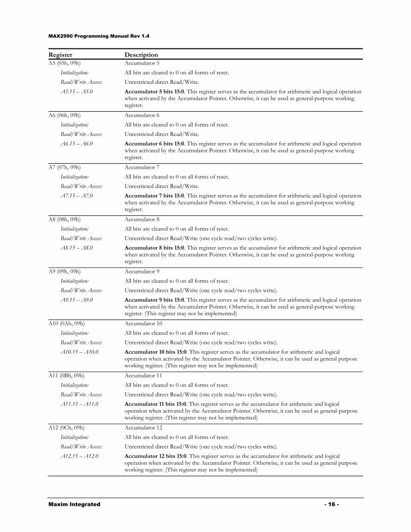
Register Description A5 (05h, 09h)
Initialization:
Read/Write Access:
A5.15 – A5.0
Accumulator 5
All bits are cleared to 0 on all forms of reset.
Unrestricted direct Read/Write.
Accumulator 5 bits 15:0. This register serves as the accumulator for arithmetic and logical operation when activated by the Accumulator Pointer. Otherwise, it can be used as general-purpose working register.
A6 (06h, 09h)
Initialization:
Read/Write Access:
A6.15 – A6.0
Accumulator 6
All bits are cleared to 0 on all forms of reset.
Unrestricted direct Read/Write.
Accumulator 6 bits 15:0. This register serves as the accumulator for arithmetic and logical operation when activated by the Accumulator Pointer. Otherwise, it can be used as general-purpose working register.
A7 (07h, 09h)
Initialization:
Read/Write Access:
A7.15 – A7.0
Accumulator 7
All bits are cleared to 0 on all forms of reset.
Unrestricted direct Read/Write.
Accumulator 7 bits 15:0. This register serves as the accumulator for arithmetic and logical operation when activated by the Accumulator Pointer. Otherwise, it can be used as general-purpose working register.
A8 (08h, 09h)
Initialization:
Read/Write Access:
A8.15 – A8.0
Accumulator 8
All bits are cleared to 0 on all forms of reset.
Unrestricted direct Read/Write (one cycle read/two cycles write).
Accumulator 8 bits 15:0. This register serves as the accumulator for arithmetic and logical operation when activated by the Accumulator Pointer. Otherwise, it can be used as general-purpose working register.
A9 (09h, 09h)
Initialization:
Read/Write Access:
A9.15 – A9.0
Accumulator 9
All bits are cleared to 0 on all forms of reset.
Unrestricted direct Read/Write (one cycle read/two cycles write).
Accumulator 9 bits 15:0. This register serves as the accumulator for arithmetic and logical operation when activated by the Accumulator Pointer. Otherwise, it can be used as general-purpose working register. (This register may not be implemented)
A10 (0Ah, 09h)
Initialization:
Read/Write Access:
A10.15 – A10.0
Accumulator 10
All bits are cleared to 0 on all forms of reset.
Unrestricted direct Read/Write (one cycle read/two cycles write).
Accumulator 10 bits 15:0. This register serves as the accumulator for arithmetic and logical operation when activated by the Accumulator Pointer. Otherwise, it can be used as general purpose working register. (This register may not be implemented)
A11 (0Bh, 09h)
Initialization:
Read/Write Access:
A11.15 – A11.0
Accumulator 11
All bits are cleared to 0 on all forms of reset.
Unrestricted direct Read/Write (one cycle read/two cycles write).
Accumulator 11 bits 15:0. This register serves as the accumulator for arithmetic and logical operation when activated by the Accumulator Pointer. Otherwise, it can be used as general-purpose working register. (This register may not be implemented)
A12 (0Ch, 09h)
Initialization:
Read/Write Access:
A12.15 – A12.0
Accumulator 12
All bits are cleared to 0 on all forms of reset.
Unrestricted direct Read/Write (one cycle read/two cycles write).
Accumulator 12 bits 15:0. This register serves as the accumulator for arithmetic and logical operation when activated by the Accumulator Pointer. Otherwise, it can be used as general purpose working register. (This register may not be implemented)
MAX2990 Programming Manual Rev 1.4
Maxim Integrated - 17 -
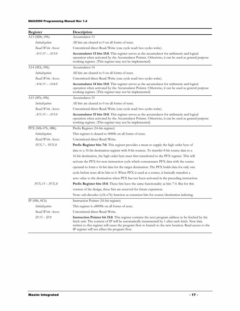
Register Description A13 (0Dh, 09h)
Initialization:
Read/Write Access:
A13.15 – A13.0
Accumulator 13
All bits are cleared to 0 on all forms of reset.
Unrestricted direct Read/Write (one cycle read/two cycles write).
Accumulator 13 bits 15:0. This register serves as the accumulator for arithmetic and logical operation when activated by the Accumulator Pointer. Otherwise, it can be used as general purpose working register. (This register may not be implemented)
A14 (0Eh, 09h)
Initialization:
Read/Write Access:
A14.15 – A14.0
Accumulator 14
All bits are cleared to 0 on all forms of reset.
Unrestricted direct Read/Write (one cycle read/two cycles write).
Accumulator 14 bits 15:0. This register serves as the accumulator for arithmetic and logical operation when activated by the Accumulator Pointer. Otherwise, it can be used as general purpose working register. (This register may not be implemented)
A15 (0Fh, 09h)
Initialization:
Read/Write Access:
A15.15 – A15.0
Accumulator 15
All bits are cleared to 0 on all forms of reset.
Unrestricted direct Read/Write (one cycle read/two cycles write).
Accumulator 15 bits 15:0. This register serves as the accumulator for arithmetic and logical operation when activated by the Accumulator Pointer. Otherwise, it can be used as general purpose working register. (This register may not be implemented)
PFX (00h-07h, 0Bh)
Initialization:
Read/Write Access:
PFX.7 – PFX.0
PFX.15 – PFX.8
Prefix Register (16-bit register)
This register is cleared to 0000h on all forms of reset.
Unrestricted direct Read/Write.
Prefix Register bits 7:0. This register provides a mean to supply the high order byte of
data to a 16-bit destination register with 8-bit sources. To transfer 8-bit source data to a
16-bit destination, the high order byte must first transferred to the PFX register. This will
activate the PFX for next instruction cycle which concatenates PFX data with the source
operand to form a 16-bit data for the target destination. The PFX holds data for only one
cycle before reset all its bits to 0. When PFX is used as a source, it basically transfers a
zero value to the destination when PFX has not been activated in the preceding instruction.
Prefix Register bits 15:8. These bits have the same functionality as bits 7-0. But for this
version of the design, these bits are reserved for future expansion.
Note: sub-decodes (x1h-x7h) function as extension bits for source/destination indexing.
IP (00h, 0Ch)
Initialization:
Read/Write Access:
IP.15 – IP.0
Instruction Pointer (16-bit register)
This register is x8000h on all forms of reset.
Unrestricted direct Read/Write.
Instruction Pointer bit 15:0. This register contains the next program address to be fetched by the fetch unit. The content of IP will be automatically incremented by 1 after each fetch. New data written to this register will cause the program flow to branch to the new location. Read access to the IP register will not affect the program flow.

MAX2990 Programming Manual Rev 1.4
Maxim Integrated - 18 -
Register Description SP (01h, 0Dh)
Initialization:
Read/Write Access:
SP.3 – SP.0
SP.15 – SP.4
Stack Pointer (16-bit register)
This register is cleared to Fh on all forms of reset.
Unrestricted direct Read/Write.
Stack Pointer Bit 3:0. The SP designates the memory location that is at the top of the stack
which is the storage location of the last word. The contents of the SP is post-decremented for a
Pop operation, and is pre-incremented for a Push operation.
(This is for 16-level stack implementation only. The level of stack required for an implementation
determines the length of SP requirement.)
Reserved, read returns 0.
IV (02h, 0Dh)
Initialization:
Read/Write Access:
IV.15 – IV.0
Interrupt Vector Register (16-bit register)
This register is 0000h on all forms of reset.
Unrestricted direct Read/Write.
Interrupt Vector bit 15:0. This register contains the interrupt vector address. The interrupt handler will force a hardware call to this vector location when there is an enabled interrupt request pending.
LC0 (06h, 0Dh)
Initialization:
Read/Write Access:
LC0.15 – LC0.0
Loop Counter 0 (16-bit register)
This register is 0000h on all forms of reset.
Unrestricted direct Read/Write.
Loop Counter 0 bit 15:0. This register contains the loop count for a loop operation. The content of LC0 will be automatically decremented by 1 after each loop. This register is normally used as loop control for conditional branch to a new location.
LC1 (07h, 0Dh)
Initialization:
Read/Write Access:
LC1.15 – LC1.0
Loop Counter 1 (16-bit register)
This register is 0000h on all forms of reset.
Unrestricted direct Read/Write.
Loop Counter 1 bit 15:0. This register contains the loop count for a loop operation. The content of LC1 will be automatically decremented by 1 after each loop. This register is normally used as loop control for conditional branch to a new location.
Offs (03h, 0Eh)
Initialization:
Read/Write Access:
Offs.7 – Offs.0
Frame Pointer Offset Register (8-bit register)
This register is 00h on all forms of reset.
Unrestricted direct Read/Write.
Frame Pointer Offset Register Bit 7:0. This 8-bit register is intended primarily for supporting Frame Pointer (FP) function which is formed by unsigned addition of Frame Pointer Base Register (BP) and Frame Pointer Offset Register (Offs). The contents of this register can be pre-incremented/decremented when using the Frame Pointer for write operation and post-incremented/decremented when using the Frame Pointer for read.
MAX2990 Programming Manual Rev 1.4
Maxim Integrated - 19 -
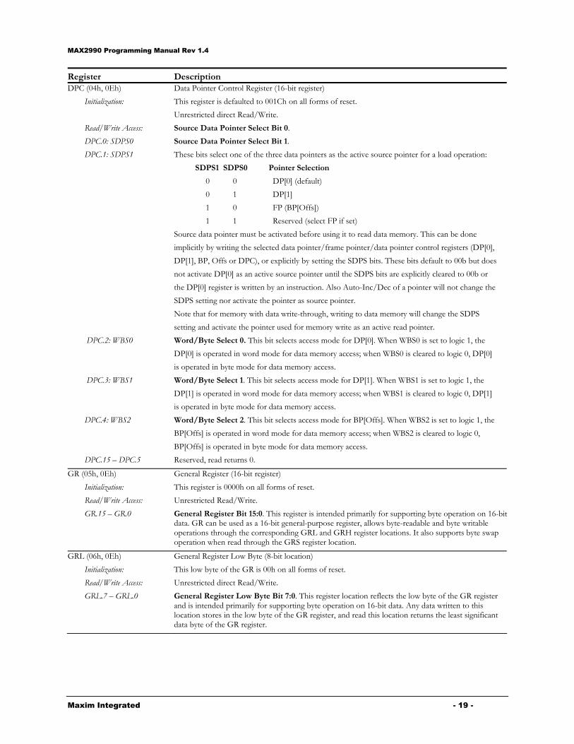
Register Description DPC (04h, 0Eh)
Initialization:
Read/Write Access:
DPC.0: SDPS0
DPC.1: SDPS1
DPC.2: WBS0
DPC.3: WBS1
DPC.4: WBS2
DPC.15 – DPC.5
Data Pointer Control Register (16-bit register)
This register is defaulted to 001Ch on all forms of reset.
Unrestricted direct Read/Write.
Source Data Pointer Select Bit 0.
Source Data Pointer Select Bit 1.
These bits select one of the three data pointers as the active source pointer for a load operation:
SDPS1 SDPS0 Pointer Selection
0 0 DP[0] (default)
0 1 DP[1]
1 0 FP (BP[Offs])
1 1 Reserved (select FP if set)
Source data pointer must be activated before using it to read data memory. This can be done
implicitly by writing the selected data pointer/frame pointer/data pointer control registers (DP[0],
DP[1], BP, Offs or DPC), or explicitly by setting the SDPS bits. These bits default to 00b but does
not activate DP[0] as an active source pointer until the SDPS bits are explicitly cleared to 00b or
the DP[0] register is written by an instruction. Also Auto-Inc/Dec of a pointer will not change the
SDPS setting nor activate the pointer as source pointer.
Note that for memory with data write-through, writing to data memory will change the SDPS
setting and activate the pointer used for memory write as an active read pointer.
Word/Byte Select 0. This bit selects access mode for DP[0]. When WBS0 is set to logic 1, the
DP[0] is operated in word mode for data memory access; when WBS0 is cleared to logic 0, DP[0]
is operated in byte mode for data memory access.
Word/Byte Select 1. This bit selects access mode for DP[1]. When WBS1 is set to logic 1, the
DP[1] is operated in word mode for data memory access; when WBS1 is cleared to logic 0, DP[1]
is operated in byte mode for data memory access.
Word/Byte Select 2. This bit selects access mode for BP[Offs]. When WBS2 is set to logic 1, the
BP[Offs] is operated in word mode for data memory access; when WBS2 is cleared to logic 0,
BP[Offs] is operated in byte mode for data memory access.
Reserved, read returns 0.
GR (05h, 0Eh)
Initialization:
Read/Write Access:
GR.15 – GR.0
General Register (16-bit register)
This register is 0000h on all forms of reset.
Unrestricted Read/Write.
General Register Bit 15:0. This register is intended primarily for supporting byte operation on 16-bit data. GR can be used as a 16-bit general-purpose register, allows byte-readable and byte writable operations through the corresponding GRL and GRH register locations. It also supports byte swap operation when read through the GRS register location.
GRL (06h, 0Eh)
Initialization:
Read/Write Access:
GRL.7 – GRL.0
General Register Low Byte (8-bit location)
This low byte of the GR is 00h on all forms of reset.
Unrestricted direct Read/Write.
General Register Low Byte Bit 7:0. This register location reflects the low byte of the GR register and is intended primarily for supporting byte operation on 16-bit data. Any data written to this location stores in the low byte of the GR register, and read this location returns the least significant data byte of the GR register.
MAX2990 Programming Manual Rev 1.4
Maxim Integrated - 20 -
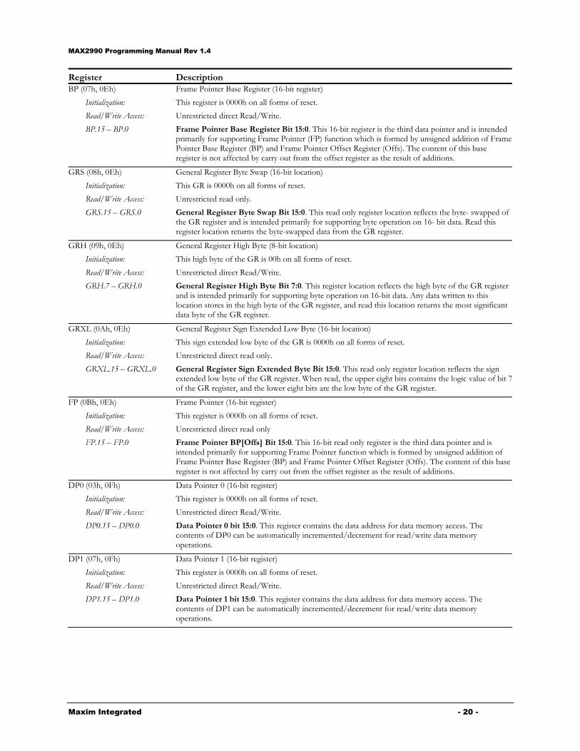
Register Description BP (07h, 0Eh)
Initialization:
Read/Write Access:
BP.15 – BP.0
Frame Pointer Base Register (16-bit register)
This register is 0000h on all forms of reset.
Unrestricted direct Read/Write.
Frame Pointer Base Register Bit 15:0. This 16-bit register is the third data pointer and is intended primarily for supporting Frame Pointer (FP) function which is formed by unsigned addition of Frame Pointer Base Register (BP) and Frame Pointer Offset Register (Offs). The content of this base register is not affected by carry out from the offset register as the result of additions.
GRS (08h, 0Eh)
Initialization:
Read/Write Access:
GRS.15 – GRS.0
General Register Byte Swap (16-bit location)
This GR is 0000h on all forms of reset.
Unrestricted read only.
General Register Byte Swap Bit 15:0. This read only register location reflects the byte- swapped of the GR register and is intended primarily for supporting byte operation on 16- bit data. Read this register location returns the byte-swapped data from the GR register.
GRH (09h, 0Eh)
Initialization:
Read/Write Access:
GRH.7 – GRH.0
General Register High Byte (8-bit location)
This high byte of the GR is 00h on all forms of reset.
Unrestricted direct Read/Write.
General Register High Byte Bit 7:0. This register location reflects the high byte of the GR register and is intended primarily for supporting byte operation on 16-bit data. Any data written to this location stores in the high byte of the GR register, and read this location returns the most significant data byte of the GR register.
GRXL (0Ah, 0Eh)
Initialization:
Read/Write Access:
GRXL.15 – GRXL.0
General Register Sign Extended Low Byte (16-bit location)
This sign extended low byte of the GR is 0000h on all forms of reset.
Unrestricted direct read only.
General Register Sign Extended Byte Bit 15:0. This read only register location reflects the sign extended low byte of the GR register. When read, the upper eight bits contains the logic value of bit 7 of the GR register, and the lower eight bits are the low byte of the GR register.
FP (0Bh, 0Eh)
Initialization:
Read/Write Access:
FP.15 – FP.0
Frame Pointer (16-bit register)
This register is 0000h on all forms of reset.
Unrestricted direct read only
Frame Pointer BP[Offs] Bit 15:0. This 16-bit read only register is the third data pointer and is intended primarily for supporting Frame Pointer function which is formed by unsigned addition of Frame Pointer Base Register (BP) and Frame Pointer Offset Register (Offs). The content of this base register is not affected by carry out from the offset register as the result of additions.
DP0 (03h, 0Fh)
Initialization:
Read/Write Access:
DP0.15 – DP0.0
Data Pointer 0 (16-bit register)
This register is 0000h on all forms of reset.
Unrestricted direct Read/Write.
Data Pointer 0 bit 15:0. This register contains the data address for data memory access. The contents of DP0 can be automatically incremented/decrement for read/write data memory operations.
DP1 (07h, 0Fh)
Initialization:
Read/Write Access:
DP1.15 – DP1.0
Data Pointer 1 (16-bit register)
This register is 0000h on all forms of reset.
Unrestricted direct Read/Write.
Data Pointer 1 bit 15:0. This register contains the data address for data memory access. The contents of DP1 can be automatically incremented/decrement for read/write data memory operations.

MAX2990 Programming Manual Rev 1.4
Maxim Integrated - 21 -
Special Function Registers:
Register Description PO0 (00h, 00h)
Initialization:
Read/Write Access:
PO0.7 – PO0.0
Port 0 Output Register
This register is cleared to FFh on all forms of reset.
Unrestricted Read/Write
Port 0 Output Register Bits 7:0. Port 0 is a type D I/O port since they require external interrupt support logic. The PO0 register stores output data for Port 0 when it is defined as an output port and controls whether the internal weak P-channel pullup transistor is enabled/disabled if a port pin is defined as an input. The contents of this register can be modified by a write access. Readingfrom the register returns the contents of the register. Changing the direction of Port 0 does not change the data contents of the register.
PO1 (01h, 00h)
Initialization:
Read/Write Access:
PO1.7 – PO1.0
Port 1 Output Register
This register is cleared to FFh on all forms of reset.
Unrestricted Read/Write
Port 1 Output Register Bits 7:0. Port 1 is a type C I/O port. The PO1 register stores output data for Port 1 when it is defined as an output port and controls whether the internal weak P-channel pullup transistor is enabled/disabled if a port pin is defined as an input. The contents of this register can be modified by a write access. Reading from the register returns the contents of the register. Changing the direction of Port 1 does not change the data contents of the register.
PO2 (02h, 00h)
Initialization:
Read/Write Access:
PO2.7 – PO2.0
Port 2 Output Register
This register is cleared to FFh on all forms of reset.
Unrestricted Read/Write
Port 2 Output Register Bits 7:0. Port 2 is a type C I/O port. The PO2 register stores output data for Port 2 when it is defined as an output port and controls whether the internal weak P-channel pullup transistor is enabled/disabled if a port pin is defined as an input. The contents of this register can be modified by a write access. Reading from the register returns the contents of the register. Changing the direction of Port 1 does not change the data contents of the register.
PO3 (03h, 00h)
Initialization:
Read/Write Access:
PO3.8 – PO3.0
Port 3 Output Register
This register is cleared to FFFFh on all forms of reset.
Unrestricted Read/Write
Port 3 Output Register Bits 8:0. Port 3 is a type C I/O port. The PO3 register stores output data for Port 3 when it is defined as an output port and controls whether the internal weak P-channel pullup transistor is enabled/disabled if a port pin is defined as an input. The contents of this register can be modified by a write access. Reading from the register returns the contents of the register. Changing the direction of Port 3 does not change the data contents of the register.
PO3.9 –PO3.15 Reserved, Read Returns 0.
EIF0 (04h, 00h)
Initialization:
Read/Write Access:
External Interrupt Flag 0 Register
EIF0 is cleared to 00h on all forms of reset.
Unrestricted read/write.
EIF0.0: IE0
Interrupt 0 Edge Detect. This bit is set when a negative edge (IT0=1) or a positive edge (IT0=0) isdetected on the Interrupt 0 pin. Setting this bit to 1 will generate an interrupt to the CPU if enabled.This bit will remain set until cleared by software or a reset. It must be cleared by software before exiting the interrupt source routine or another interrupt will be generated as long as this bit is set.
EIF0.1: IE1
Interrupt 1 Edge Detect. This bit is set when a negative edge (IT1=1) or a positive edge (IT1=0) is detected on the Interrupt 1 pin. Setting this bit to 1 will generate an interrupt to the CPU if enabled.This bit will remain set until cleared by software or a reset. It must be cleared by software beforeexiting the interrupt source routine or another interrupt will be generated as long as this bit is set.

MAX2990 Programming Manual Rev 1.4
Maxim Integrated - 22 -
Register Description EIF0.2: IE2
Interrupt 2 Edge Detect. This bit is set when a negative edge (IT2=1) or a positive edge (IT2=0) isdetected on the Interrupt 2 pin. Setting this bit to 1 will generate an interrupt to the CPU if enabled. This bit will remain set until cleared by software or a reset. It must be cleared by software beforeexiting the interrupt source routine or another interrupt will be generated as long as this bit is set.
EIF0.3: IE3
Interrupt 3 Edge Detect. This bit is set when a negative edge (IT3=1) or a positive edge (IT3=0) isdetected on the Interrupt 3 pin. Setting this bit to 1 will generate an interrupt to the CPU if enabled.This bit will remain set until cleared by software or a reset. It must be cleared by software beforeexiting the interrupt source routine or another interrupt will be generated as long as this bit is set.
EIF0.4: IE4
Interrupt 4 Edge Detect. This bit is set when a negative edge (IT4=1) or a positive edge (IT4=0) is detected on the Interrupt 4 pin. Setting this bit to 1 will generate an interrupt to the CPU if enabled.This bit will remain set until cleared by software or a reset. It must be cleared by software beforeexiting the interrupt source routine or another interrupt will be generated as long as this bit is set.
EIF0.5: IE5
Interrupt 5 Edge Detect. This bit is set when a negative edge (IT5=1) or a positive edge (IT5=0) isdetected on the Interrupt 5 pin. Setting this bit to 1 will generate an interrupt to the CPU if enabled.This bit will remain set until cleared by software or a reset. It must be cleared by software beforeexiting the interrupt source routine or another interrupt will be generated as long as this bit is set.
EIF0.6: IE6
Interrupt 6 Edge Detect. This bit is set when a negative edge (IT6=1) or a positive edge (IT6=0) isdetected on the Interrupt 6 pin. Setting this bit to 1 will generate an interrupt to the CPU if enabled. This bit will remain set until cleared by software or a reset. It must be cleared by software beforeexiting the interrupt source routine or another interrupt will be generated as long as this bit is set.
EIF0.7: IE7 Interrupt 7 Edge Detect. This bit is set when a negative edge (IT7=1) or a positive edge (IT7=0) isdetected on the Interrupt 7 pin. Setting this bit to 1 will generate an interrupt to the CPU if enabled.This bit will remain set until cleared by software or a reset. It must be cleared by software before exiting the interrupt source routine or another interrupt will be generated as long as this bit is set.
EIE0 (05h, 00h)
Initialization:
Read/Write Access:
External Interrupt Enable 0 Register
EIE0 is cleared to 00h on all forms of reset.
Unrestricted read/write.
EIE0.0: EX0 Enable External Interrupt 0. Setting this bit to 1 enables external interrupt 0. Clearing this bit to 0disables the interrupt function.
EIE0.1: EX1 Enable External Interrupt 1. Setting this bit to 1 enables external interrupt 1. Clearing this bit to 0disables the interrupt function.
EIE0.2: EX2 Enable External Interrupt 2. Setting this bit to 1 enables external interrupt 2. Clearing this bit to 0 disables the interrupt function.
EIE0.3: EX3 Enable External Interrupt 3. Setting this bit to 1 enables external interrupt 3. Clearing this bit to 0disables the interrupt function.
EIE0.4: EX4 Enable External Interrupt 4. Setting this bit to 1 enables external interrupt 4. Clearing this bit to 0 disables the interrupt function.
EIE0.5: EX5 Enable External Interrupt 5. Setting this bit to 1 enables external interrupt 5. Clearing this bit to 0disables the interrupt function.
EIE0.6: EX6 Enable External Interrupt 6. Setting this bit to 1 enables external interrupt 6. Clearing this bit to 0disables the interrupt function.
EIE0.7: EX7 Enable External Interrupt 7. Setting this bit to 1 enables external interrupt 7. Clearing this bit to 0 disables the interrupt function.
PI0 (08h, 00h)
Initialization:
Read/Write Access:
PI0.7 – PI0.0
Port 0 Input Register
The reset value for this register is dependent on the logical states of the pins.
Unrestricted Read only
Port 0 Input Register Bits 7:0. The PI0 register always reflects the logic state of its pins when read. Note that each port pin has a weak pullup circuit when functioning as an input and the P channel pullup transistor is controlled by its respective PO bits. If the PO bit is set to 1, the weak pullup is on, if the PO bit is cleared to 0, the weak pullup is off and forces the port pin into tri-state.

MAX2990 Programming Manual Rev 1.4
Maxim Integrated - 23 -
Register Description PI1 (09h, 00h)
Initialization:
Read/Write Access:
PI1.7 – PI1.0
Port 1 Input Register
The reset value for this register is dependent on the logical states of the pins.
Unrestricted Read
Port 1 Input Register Bits 7:0. Port 1 is a type C I/O port. The PI1 register always reflects the logic state of its pins when read. Note that each port pin has a weak pullup circuit when functioning as an input and the P channel pullup transistor is controlled by its respective PO bits. If the PO bit is set to 1, the weak pullup is on, if the PO bit is cleared to 0, the weak pullup is off and forces the port pin into tri-state.
PI2 (0Ah, 00h)
Initialization:
Read/Write Access:
PI2.7 – PI2.0
Port 2 Input Register
The reset value for this register is dependent on the logical states of the pins.
Unrestricted Read
Port 2 Input Register Bits 7:0. Port 2 is a type C I/O port. The PI2 register always reflects the logic state of its pins when read. Note that each port pin has a weak pullup circuit when functioning as an input and the P channel pullup transistor is controlled by its respective PO bits. If the PO bit is set to 1, the weak pullup is on, if the PO bit is cleared to 0, the weak pullup is off and forces the port pin into tri-state.
PI3 (0Bh, 00h)
Initialization:
Read/Write Access:
PI3.8 – PI3.0
Port 3 Input Register
The reset value for this register is dependent on the logical states of the pins.
Unrestricted Read
Port 3 Input Register Bits 8:0. Port 3 is a type C I/O port. The PI3 register always reflects the logic state of its pins when read. Note that each port pin has a weak pullup circuit when functioning as an input and the P channel pullup transistor is controlled by its respective PO bits. If the PO bit is set to 1, the weak pullup is on, if the PO bit is cleared to 0, the weak pullup is off and forces the port pin into tri-state.
PI3.9 –PI3.15 Reserved, Read Returns 0.
EIES0 (0Ch, 00h)
Initialization:
Read/Write Access:
External Interrupt Edge Select 0 Register
EIES0 is cleared to 00h on all forms of reset.
Unrestricted read/write.
EIES0.0: IT0
Edge Select for External Interrupt 0
IT0 = 0: External Interrupt 0 is positive edge triggered.
IT0 = 1: External Interrupt 0 is negative edge triggered.
EIES0.1: IT1
Edge Select for External Interrupt 1
IT1 = 0: External Interrupt 1 is positive edge triggered.
IT1 = 1: External Interrupt 1 is negative edge triggered.
EIES0.2: IT2
Edge Select for External Interrupt 2
IT2 = 0: External Interrupt 2 is positive edge triggered.
IT2 = 1: External Interrupt 2 is negative edge triggered.
EIES0.3: IT3
Edge Select for External Interrupt 3
IT3 = 0: External Interrupt 3 is positive edge triggered.
IT3 = 1: External Interrupt 3 is negative edge triggered.
EIES0.4: IT4
Edge Select for External Interrupt 4
IT4 = 0: External Interrupt 4 is positive edge triggered.
IT4 = 1: External Interrupt 4 is negative edge triggered.
EIES0.5: IT5
Edge Select for External Interrupt 5
IT5 = 0: External Interrupt 5 is positive edge triggered.
IT5 = 1: External Interrupt 5 is negative edge triggered.

MAX2990 Programming Manual Rev 1.4
Maxim Integrated - 24 -
Register Description EIES0.6: IT6
Edge Select for External Interrupt 6
IT6 = 0: External Interrupt 6 is positive edge triggered.
IT6 = 1: External Interrupt 6 is negative edge triggered.
EIES0.7: IT7
Edge Select for External Interrupt 7
IT7 = 0: External Interrupt 7 is positive edge triggered.
IT7 = 1: External Interrupt 7 is negative edge triggered.
EGCKCN (0Dh, 00h)
Initialization:
Read/Write Access:
EGCKCN.0: X1EGCKSEL
EGCKCN.1: X2EGCKSEL
EGCKCN.2 – 7
External GPIO Clock Control Register
This register is cleared to 00h on POR reset. It is unaffected by all other forms of reset.
Unrestricted read/write access.
XTAL1 External GPIO Clock Select Bit. If set, his bit activates the external 3.3V clock input for the system clock on pin P2.4. This bit over-rides the X1BY bit in the PMR register and forces the base system clock (prior to the PLL or PMM divider) to be source from the GPIO pin. Any clock or crystal connected to XTAL1 will be ignored.
XTAL2 External GPIO Clock Select Bit. If set, his bit activates the external 3.3V clock input for the AFE clock on pin P2.6. This bit over-rides the X2BY bit in the PMR register and forces the base AFE clock (prior to the PLL or PMM divider) to be source from the GPIO pin. Any clock or crystal connected to XTAL2 will be ignored.
Reserved, read returns zero.
PD0 (10h, 00h)
Initialization:
Read/Write Access:
PD0.7 – PD0.0
Port 0 Direction Register
This register is cleared to 00h on all forms of reset.
Unrestricted Read/Write
Port 0 Direction Register Bits 7:0. PD0 is used to determine the direction of the Port 0 function. The port pins are independently controlled by their direction bit. When a bit is set to 1, its corresponding pin is used as an output; data in the PO register will be driven on the pin. When a bit is cleared to 0, its corresponding pin is used as an input, and allows an external signal to drive the pin. Note that each port pin has a weak pullup circuit when functioning as an input and the P channel pullup transistor is controlled by its respective PO bits. If the PO bit is set to 1, the weak pullup is on, if the PO bit is cleared to 0, the weak pullup is off and forces the port pin into tri-state.
PD1 (11h, 00h)
Initialization:
Read/Write Access:
PD1.7 – PD1.0
Port 1 Direction Register
This register is cleared to 00h on all forms of reset.
Unrestricted Read/Write
Port 1 Direction Register Bits 7:0. Port 1 is a type C I/O port. PD1 is used to determine the direction of the Port 1 function. The port pins are independently controlled by their direction bit. When a bit is set to 1, its corresponding pin is used as an output; data in the PO register will be driven on the pin. When a bit is cleared to 0, its corresponding pin is used as an input, and allows an external signal to drive the pin. Note that each port pin has a weak pullup circuit when functioning as an input and the P channel pullup transistor is controlled by its respective PO bits. If the PO bit is set to 1, the weak pullup is on, if the PO bit is cleared to 0, the weak pullup is off and forces the port pin into tri-state.
PD2 (12h, 00h)
Initialization:
Read/Write Access:
PD2.7 – PD2.0
Port 2 Direction Register
This register is cleared to 00h on all forms of reset.
Unrestricted Read/Write
Port 2 Direction Register Bits 7:0. Port 2 is a type C I/O port. PD2 is used to determine the direction of the Port 2 function. The port pins are independently controlled by their direction bit. When a bit is set to 1, its corresponding pin is used as an output; data in the PO register will be driven on the pin. When a bit is cleared to 0, its corresponding pin is used as an input, and allows an external signal to drive the pin. Note that each port pin has a weak pullup circuit when functioning as an input and the P channel pullup transistor is controlled by its respective PO bits. If the PO bit is set to 1, the weak pullup is on, if the PO bit is cleared to 0, the weak pullup is off and forces the port pin into tri-state.

MAX2990 Programming Manual Rev 1.4
Maxim Integrated - 25 -
Register Description PD3 (13h, 00h)
Initialization:
Read/Write Access:
PD3.8 – PD3.0
Port 3 Direction Register
This register is cleared to 0000h on all forms of reset.
Unrestricted Read/Write
Port 3 Direction Register Bits 8:0. Port 3 is a type C I/O port. PD3 is used to determine the direction of the Port 3 function. The port pins are independently controlled by their direction bit. When a bit is set to 1, its corresponding pin is used as an output; data in the PO register will be driven on the pin. When a bit is cleared to 0, its corresponding pin is used as an input, and allows an external signal to drive the pin. Note that each port pin has a weak pullup circuit when functioning as an input and the P channel pullup transistor is controlled by its respective PO bits. If the PO bit is set to 1, the weak pullup is on, if the PO bit is cleared to 0, the weak pullup is off and forces the port pin into tri-state.
RTRM (18h, 00h)
Initialization:
Real Time Clock Trim Register (8-bit register)
This register is battery-backed through POR so long as VBAT(min) < VBAT <VBAT(max), however it is indeterminate on the very first POR and must be configured initially by the user. This register is unaffected by other resets.
Read/Write Access: Unrestricted read/write access.
RTRM.6-0: TRM6:0 RTC Trim Calibration Register Bits 6:0. These register bits provide a binary value between 00h-7Fh which is used for adjusting 32K clocks insertion/removal. At every 10 second intervals, number of 32K clocks equal to the TRM[6:0] numeric value will be inserted/removed from the RTC counter depending on the value in the TSGN bit.
The Trim bits are write protected by WE. WE must be set to 1 in order for the bits to be updated.
RTRM.7:TSGN RTC Trim Sign Bit. This register bit selects whether 32K clock will be inserted (TSGN=1) or removed (TSGN=0).
RCNT (19h, 00h)
Initialization:
Read/Write Access:
Real Time Clock Control Register
Bits 15, 12:4, 2:1 are reset to 0b on any reset. Bit 3 (BUSY) is set to 1 on system reset. Bits 14,
13 and 0are unaffected by resets other than Power-On Reset.
Unrestricted Read. Bit 3 (BUSY) is read only. Bit 15 (WE), bit 5 (RDYE), and bit 4 (RDY) are unrestricted write. Bit 0 (RTCE) is write accessible only when WE=1 and BUSY=0. Bits 14 (X32D) and 13 (ACS) are write accessible only when RTCE=0. All other bits are write accessible only when BUSY=0. An attempted write operation is not complete until hardware clears the BUSY bit.
RCNT.0: RTCE
Real Time Clock Enable. The RTCE is the Real Time Enable bit, setting this bit to logic 1 activates the clocking by allowing the divided clock to the ripple counters. Clearing this bit to logic 0 disables the clock.
RCNT.1: ADE
Alarm Time-of-Day Enable. The ADE bit is the RTC’s Time-of-Day alarm enable and must be set to logic 1 in order for the alarm to generate a system interrupt request. When the ADE is cleared to logic 0, the Time-of-Day alarm is disabled, no interrupt is generated even the alarm is set.
RCNT.2: ASE
Alarm Sub-second Enable. The ASE bit is the RTC’s sub-second timer enable and must beset to logic 1 in order for the sub-second alarm to generate a system interrupt request. When the ASE is cleared to logic 0, the sub-second alarm is disabled, no interrupt is generated even the alarm is set.
RCNT.3: BUSY
RTC Busy. This bit is set to 1 by hardware when any of the following conditions occur:
1) System reset,
2) Software writes to RTC count registers or
3) Software changes RTCE, ASE, or ADE.
For conditions 2) and 3), the write or change should not be considered complete until hardware clears the BUSY bit. This is an indication that a 32kHz synchronized version of the register bit(s) is in place.
RCNT.4:RDY
RTC Ready. This bit is set to 1 by hardware when the RTC count registers update. It can be cleared to 0 by software at any time. It will also be cleared to 0 by hardware just prior to an update of the RTC count register. This bit can generate an interrupt if the RDYE bit is set to 1.
RCNT.5: RDYE
RTC Ready Enable. Setting this bit to 1 allows a system interrupt to be generated when RDY becomes active (if interrupts are enabled globally and modularly). Clearing this bit to 0 disables the RDY interrupt.
MAX2990 Programming Manual Rev 1.4
Maxim Integrated - 26 -
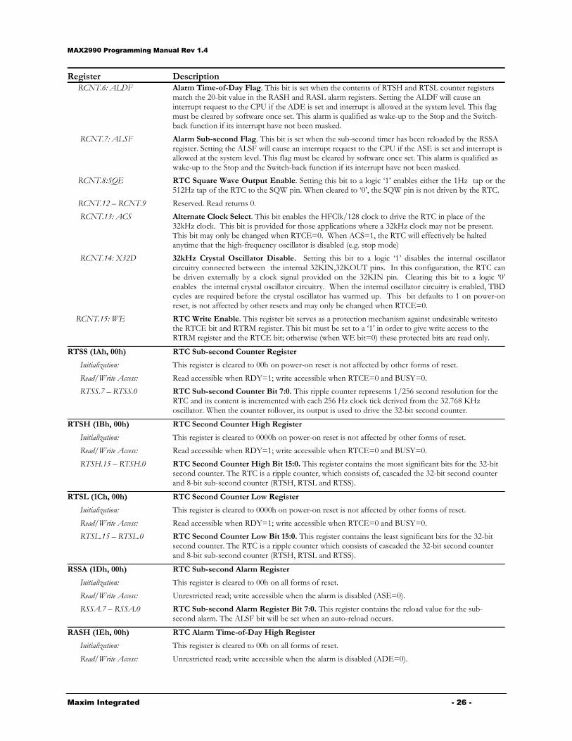
Register Description RCNT.6: ALDF
Alarm Time-of-Day Flag. This bit is set when the contents of RTSH and RTSL counter registers match the 20-bit value in the RASH and RASL alarm registers. Setting the ALDF will cause an interrupt request to the CPU if the ADE is set and interrupt is allowed at the system level. This flag must be cleared by software once set. This alarm is qualified as wake-up to the Stop and the Switch-back function if its interrupt have not been masked.
RCNT.7: ALSF
Alarm Sub-second Flag. This bit is set when the sub-second timer has been reloaded by the RSSA register. Setting the ALSF will cause an interrupt request to the CPU if the ASE is set and interrupt is allowed at the system level. This flag must be cleared by software once set. This alarm is qualified as wake-up to the Stop and the Switch-back function if its interrupt have not been masked.
RCNT.8:SQE RTC Square Wave Output Enable. Setting this bit to a logic ‘1’ enables either the 1Hz tap or the 512Hz tap of the RTC to the SQW pin. When cleared to ‘0’, the SQW pin is not driven by the RTC.
RCNT.12 – RCNT.9 Reserved. Read returns 0.
RCNT.13: ACS
Alternate Clock Select. This bit enables the HFClk/128 clock to drive the RTC in place of the 32kHz clock. This bit is provided for those applications where a 32kHz clock may not be present. This bit may only be changed when RTCE=0. When ACS=1, the RTC will effectively be halted anytime that the high-frequency oscillator is disabled (e.g. stop mode)
RCNT.14: X32D
32kHz Crystal Oscillator Disable. Setting this bit to a logic ‘1’ disables the internal oscillator circuitry connected between the internal 32KIN,32KOUT pins. In this configuration, the RTC canbe driven externally by a clock signal provided on the 32KIN pin. Clearing this bit to a logic ‘0’ enables the internal crystal oscillator circuitry. When the internal oscillator circuitry is enabled, TBDcycles are required before the crystal oscillator has warmed up. This bit defaults to 1 on power-on reset, is not affected by other resets and may only be changed when RTCE=0.
RCNT.15: WE RTC Write Enable. This register bit serves as a protection mechanism against undesirable writesto the RTCE bit and RTRM register. This bit must be set to a ‘1’ in order to give write access to the RTRM register and the RTCE bit; otherwise (when WE bit=0) these protected bits are read only.
RTSS (1Ah, 00h)
Initialization:
Read/Write Access:
RTSS.7 – RTSS.0
RTC Sub-second Counter Register
This register is cleared to 00h on power-on reset is not affected by other forms of reset.
Read accessible when RDY=1; write accessible when RTCE=0 and BUSY=0.
RTC Sub-second Counter Bit 7:0. This ripple counter represents 1/256 second resolution for the RTC and its content is incremented with each 256 Hz clock tick derived from the 32.768 KHz oscillator. When the counter rollover, its output is used to drive the 32-bit second counter.
RTSH (1Bh, 00h)
Initialization:
Read/Write Access:
RTSH.15 – RTSH.0
RTC Second Counter High Register
This register is cleared to 0000h on power-on reset is not affected by other forms of reset.
Read accessible when RDY=1; write accessible when RTCE=0 and BUSY=0.
RTC Second Counter High Bit 15:0. This register contains the most significant bits for the 32-bit second counter. The RTC is a ripple counter, which consists of, cascaded the 32-bit second counter and 8-bit sub-second counter (RTSH, RTSL and RTSS).
RTSL (1Ch, 00h)
Initialization:
Read/Write Access:
RTSL.15 – RTSL.0
RTC Second Counter Low Register
This register is cleared to 0000h on power-on reset is not affected by other forms of reset.
Read accessible when RDY=1; write accessible when RTCE=0 and BUSY=0.
RTC Second Counter Low Bit 15:0. This register contains the least significant bits for the 32-bit second counter. The RTC is a ripple counter which consists of cascaded the 32-bit second counter and 8-bit sub-second counter (RTSH, RTSL and RTSS).
RSSA (1Dh, 00h)
Initialization:
Read/Write Access:
RSSA.7 – RSSA.0
RTC Sub-second Alarm Register
This register is cleared to 00h on all forms of reset.
Unrestricted read; write accessible when the alarm is disabled (ASE=0).
RTC Sub-second Alarm Register Bit 7:0. This register contains the reload value for the sub-second alarm. The ALSF bit will be set when an auto-reload occurs.
RASH (1Eh, 00h)
Initialization:
Read/Write Access:
RTC Alarm Time-of-Day High Register
This register is cleared to 00h on all forms of reset.
Unrestricted read; write accessible when the alarm is disabled (ADE=0).

MAX2990 Programming Manual Rev 1.4
Maxim Integrated - 27 -
Register Description RASH.3 – RASH.0
RTC Time-of-Day High Bit 3:0. This register contains the most significant bits for the 24-bit Time-of-Day alarm. The Time-of-Day alarm is formed by the RASH and the RASL registers and only the lower 20 bits is meaningful for the alarm function. The Timer-of-Day alarm is trigged when sub-second counter rollover while the lower 20-bit contents of the Time-of-Day alarm is matched the 20 least significant bits of the second counter formed by the RTSH and the RTSL registers.
RASH.7 – RASH.4 Reserved, read returns 0.
RASL (1Fh, 00h)
Initialization:
Read/Write Access:
RASL.15 – RASL.0
RTC Alarm Time-of-Day Low Register
This register is cleared to 0000h on all forms of reset.
Unrestricted Read/Write
RTC Time-of-Day Low Bit 15:0. This register contains the least significant bits for the 24-bit Time-of-Day alarm. The Time-of-Day alarm is formed by the RASH and the RASL registers and only the lower 20 bits are meaningful for the alarm function. The Timer-of-Day alarm is trigged when sub-second counter rollover while the lower 20-bit contents of the Time-of-Day alarm is matched the 20 least significant bits of the second counter formed by the RTSH and the RTSL registers.
SPIB0 (00h, 01h)
Initialization:
Read/Write Access:
SPIB0.15-SPIB0.0
SPI 0 Data Buffer
This buffer is cleared to 0000h on all forms of reset.
Unrestricted read, write is allowed outside of a transfer cycle; when the STBY bit is set, write is
blocked and will cause write collision error.
SPI 0 Data Buffer Bits 15:0. Data for SPI is read from or written to this location. The serial transmit and receive buffers are separate but both are addressed at this location.
SPICN0 (01h, 01h)
Initialization:
Read/Write Access:
SPI 0 Control Register
This buffer is cleared to 00h on all forms of reset.
Unrestricted read/write except bit 7 are read only.
SPICN0.0: SPIEN SPI 0 Enable. Setting this bit to a logic 1 enables the SPI module and its baud rate generator for SPI operation. Clearing this bit to 0 disables the SPI module and its baud rate generator.
SPICN0.1: MSTM
Master Mode Enable. MSTM functions as a master mode enable bit for the SPI module. When MSTM is set to a logic 1, the SPI operates as a master. When MSTM is cleared to 0, the SPI module operates in slave mode. Note that this bit can be set from 0 to 1 only when the SSEL signal is de-asserted.
SPICN0.2: MODFE
Mode Fault Enable. When set to a logic 1 in master mode, this bit enables the use of SSEL input as a mode fault signal; when cleared to 0, the SSEL has no function and its port pin can be used for other purposes. In slave mode, the SSEL pin always functions as a slave select input signal to the SPI module, independent of the setting of the MODFE bit.
SPICN0.3: MODF
Mode Fault Flag. This bit is the mode fault flag when the SPI is operating as a master. When mode fault detection is enabled as MODFE=1 in master mode, a detection of a high to low transition on the SSEL pin signifies a mode fault and sets the MODF to 1. This bit must be cleared to 0 by software once set. Setting this bit to a logic 1 by software will cause an interrupt if enabled. This flag has no meaning in slave mode.
SPICN0.4: WCOL
Write Collision Flag. This bit indicates a write collision when set to 1. This is caused by attempting to write to the SPIB while a transfer cycle is in progress. This bit must be cleared to 0 by software once set. Setting this bit to a logic 1 by software will cause an interrupt if enabled.
SPICN0.5: ROVR
Receive Overrun Flag. This bit indicates a receive overrun when set to 1. This is caused by two or more characters have been received since the last read by the processor. The newer data is lost. This bit must be cleared to 0 by software once set. Setting this bit to a logic 1 by software will cause an interrupt if enabled.
SPICN0.6: SPIC
SPI Transfer Complete Flag. This bit indicates the completion of a transfer cycle when set to 1. This bit must be cleared to 0 by software once set. Setting this bit to a logic 1 by software will cause an interrupt if enabled.
SPICN0.7: STBY
SPI Transfer Busy Flag. This bit is used to indicate the current status of the SPI module. STBY is set to 1 when starting a SPI transfer cycle and will be cleared to 0 when the transfer cycle iscompleted. This bit is controlled by hardware and is read only for user software.

MAX2990 Programming Manual Rev 1.4
Maxim Integrated - 28 -
Register Description SPICF0 (02h, 01h)
Initialization:
Read/Write Access:
SPI 0 Configuration Register
This buffer is cleared to 00h on all forms of reset.
Unrestricted read/write.
SPICF0.0: CKPOL
Clock Polarity Select. This bit is used with the CKPHA bit to determine the SPI transfer format. When the CKPOL is set to 1, the SPI uses the clock falling edge as an active edge. When the CKPOL is cleared to 0, the SPI selects the clock rising edge as an active edge.
SPICF0.1: CKPHA
Clock Phase Select. This bit is used with the CKPOL bit to determine the SPI transfer format. When the CKPHA is set to 1, the SPI will sample input data at an inactive edge. When the CKPHA is cleared to 0, the SPI will sample input data at an active edge.
SPICF0.2: CHR
Character Length Bit. The CHR bit determines the character length for an SPI transfer cycle. A character can consist 8 or 16 bits in length. When CHR bit is 0, the character is 8 bits; when CHR is set to 1, the character is 16 bits.
SPICF0.6-3 Reserved, Read Returns 0.
SPICF0.7: ESPII SPI Interrupt Enable. Setting this bit to 1 enables the SPI interrupt when MODF, WCOL, ROVR, or SPIC flags are set. Clearing this bit to 0 disables the SPI interrupt.
SPICK0 (03h, 01h)
Initialization:
Read/Write Access:
SPICK0.7-SPICK0.0
SPI 0 Clock Register
This buffer is cleared to 00h on all forms of reset.
Unrestricted read/write.
Clock Divide Ratio Bit 7-0. These bits select one of the 256 divide ratios (0 to 255) used for the baud rate generator, with bit 7 as the most significant bit. The frequency of the SPI baud rate is calculated using the following equation:
SPI Baud Rate = 0.5 x System Clock/(divide ratio + 1)
This register has no function when operating in slave mode and the clock generation circuitry should be disabled.
I2CBUF (04h, 01h)
Initialization:
Read/Write Access:
I2C Data Buffer Register ( 16-bit Register )
This register is cleared to 0000h on all forms of reset
Unrestricted read access. This register can be written to only when I2CBUSY=0.
I2CBUF.9 – 0 I2C Data Buffer Bits 9:0. Data for I2C transfer is read from or written to this location. The I2Ctransmit and receive buffers are separate but both are addressed at this location.
During address transmission, if I2CEA=0, I2CBUF[6:0] is used as the address bits. If I2CEA=1,I2CBUF[9:0] are used as extended address bits.
During data transmission, only I2CBUF[7:0] are used.
I2CBUF.15-I2CBUF.10 Reserved. Read return 0.
I2CST (05h, 01h)
Initialization:
Read/Write Access:
I2C Status Register (16-bit register)
This register is cleared to 0000h on all forms of reset.
Unrestricted read. Not all the bits can be written by software. For each bit accessibility, see theindividual bit description.
I2CST.0:I2CSRI I2C START Interrupt Flag. This bit is set to ‘1’ when a START condition (S or Sr) is detected.This bit must be cleared to ‘0’ by software once set. Setting this bit to ‘1’ by software will cause aninterrupt if enabled.
I2CST.1:I2CTXI I2C Transmit Complete Interrupt Flag. This bit indicates that an address or a data byte has beensuccessfully shifted out and the I2C controller has received an acknowledgment from the receiver(NACK or ACK). This bit must be cleared by software once set. Setting this bit to 1 by softwarewill cause an interrupt if enabled.
I2CST.2:I2CRXI I2C Receive Ready Interrupt Flag. This bit indicates that a data byte has been received in the I2Cbuffer. This bit must be cleared by software once set. Setting this bit to 1 by hardware will cause aninterrupt if enabled. This bit is set by hardware only.
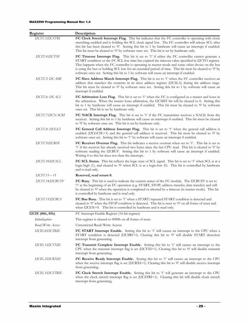
MAX2990 Programming Manual Rev 1.4
Maxim Integrated - 29 -
Register Description I2CST.3:I2CSTRI I2C Clock Stretch Interrupt Flag. This bit indicates that the I2C controller is operating with clock
stretching enabled and is holding the SCL clock signal low. The I2C controller will release SCL afterthis bit has been cleared to ‘0’. Setting this bit to 1 by hardware will cause an interrupt if enabled.This bit must be cleared to ‘0’ by software once set. This bit is set by hardware only.
I2CST.4:I2CTOI I2C Timeout Interrupt Flag. This bit is set to ‘1’ if either the I2C controller cannot generate aSTART condition or the I2C SCL low time has expired the timeout value specified in I2CTO register.This happens when the I2C controller is operating in master mode and some other device on the busis using the bus or holding SCL low for an extended period of time. This bit must be cleared to ‘0’ bysoftware once set. Setting this bit to 1 by software will cause an interrupt if enabled.
I2CST.5: I2CAMI I2C Slave Address Match Interrupt Flag. This bit is set to ‘1’ when the I2C controller receives anaddress that matches the contents in its slave address register (I2CSLA) during the address stage.This bit must be cleared to ‘0’ by software once set. Setting this bit to 1 by software will cause aninterrupt if enabled.
I2CST.6: I2CALI I2C Arbitration Loss Flag. This bit is set to ‘1’ when the I2C is configured as a master and loses inthe arbitration. When the master loses arbitration, the I2CMST bit will be cleared to 0. Setting thisbit to 1 by hardware will cause an interrupt if enabled. This bit must be cleared to ‘0’ by softwareonce set. This bit is set by hardware only.
I2CST.7:I2CNACKI I2C NACK Interrupt Flag. This bit is set to ‘1’ if the I2C transmitter receives a NACK from thereceiver. Setting this bit to 1 by hardware will cause an interrupt if enabled. This bit must be clearedto ‘0’ by software once set. This bit is set by hardware only.
I2CST.8: I2CGCI I2C General Call Address Interrupt Flag. This bit is set to ‘1’ when the general call address isenabled (I2CGCIE=1) and the general call address is received. This bit must be cleared to ‘0’ bysoftware once set. Setting this bit to ‘1’ by software will cause an interrupt if enabled.
I2CST.9:I2CROI I2C Receiver Overrun Flag. This bit indicates a receive overrun when set to ‘1’. This bit is set to‘1’ if the receiver has already received two bytes since the last CPU read. This bit is cleared to ‘0’ bysoftware reading the I2CBUF. Setting this bit to 1 by software will cause an interrupt if enabled.Writing 0 to this bit does not clear the interrupt.
I2CST.10:I2CSCL I2C SCL Status. This bit reflects the logic state of SCL signal. This bit is set to ‘1’ when SCL is at alogic-high (1), and cleared to ‘0’ when SCL is at a logic-low (0). This bit is controlled by hardwareand is read only.
I2CST.13 – 11 Reserved, read return 0.
I2CST.14:I2CBUSY I2C Busy. This bit is used to indicate the current status of the I2C module. The I2CBUSY is set to ‘1’ at the beginning of an I2C operation (e.g. START, STOP, address transfer, data transfer) and will be cleared to ‘0’ when the operation is completed or aborted by a timeout (in master mode). This bit is controlled by hardware and is read only.
I2CST.15:I2CBUS I2C Bus Busy. This bit is set to ‘1’ when a START/repeated START condition is detected and cleared to ‘0’ when the STOP condition is detected. This bit is reset to ‘0’ on all forms of reset and when I2CEN=0. This bit is controlled by hardware and is read only.
I2CIE (06h, 01h)
Initialization:
Read/Write Access:
I2C Interrupt Enable Register (16-bit register)
This register is cleared to 0000h on all forms of reset.
Unrestricted Read/Write Access.
I2CIE.0:I2CSRIE I2C START Interrupt Enable. Setting this bit to ‘1’ will causes an interrupt to the CPU when aSTART condition is detected (I2CSRI=1). Clearing this bit to ‘0’ will disable START detectioninterrupt from generating.
I2CIE.1:I2CTXIE I2C Transmit Complete Interrupt Enable. Setting this bit to ‘1’ will causes an interrupt to theCPU when the transmit interrupt flag is set (I2CTXI=1). Clearing this bit to ‘0’ will disable transmitinterrupt from generating.
I2CIE.2:I2CRXIE I2C Receive Ready Interrupt Enable. Setting this bit to ‘1’ will causes an interrupt to the CPUwhen the receive interrupt flag is set (I2CRXI=1). Clearing this bit to ‘0’ will disable receive interruptfrom generating.
I2CIE.3:I2CSTRIE I2C Clock Stretch Interrupt Enable. Setting this bit to ‘1’ will generate an interrupt to the CPUwhen the clock stretch interrupt flag is set (I2CSTRI=1). Clearing this bit will disable clock stretchinterrupt from generating.
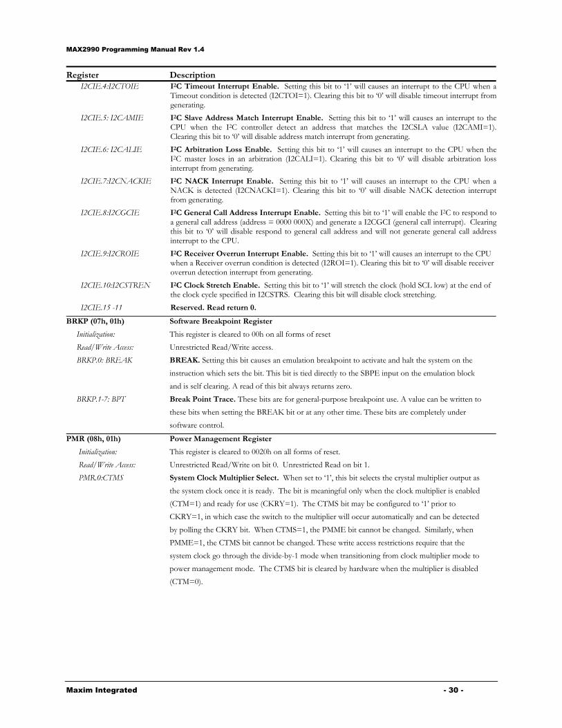
MAX2990 Programming Manual Rev 1.4
Maxim Integrated - 30 -
Register Description I2CIE.4:I2CTOIE I2C Timeout Interrupt Enable. Setting this bit to ‘1’ will causes an interrupt to the CPU when a
Timeout condition is detected (I2CTOI=1). Clearing this bit to ‘0’ will disable timeout interrupt fromgenerating.
I2CIE.5: I2CAMIE I2C Slave Address Match Interrupt Enable. Setting this bit to ‘1’ will causes an interrupt to theCPU when the I2C controller detect an address that matches the I2CSLA value (I2CAMI=1).Clearing this bit to ‘0’ will disable address match interrupt from generating.
I2CIE.6: I2CALIE I2C Arbitration Loss Enable. Setting this bit to ‘1’ will causes an interrupt to the CPU when theI2C master loses in an arbitration (I2CALI=1). Clearing this bit to ‘0’ will disable arbitration lossinterrupt from generating.
I2CIE.7:I2CNACKIE I2C NACK Interrupt Enable. Setting this bit to ‘1’ will causes an interrupt to the CPU when aNACK is detected (I2CNACKI=1). Clearing this bit to ‘0’ will disable NACK detection interruptfrom generating.
I2CIE.8:I2CGCIE I2C General Call Address Interrupt Enable. Setting this bit to ‘1’ will enable the I2C to respond toa general call address (address = 0000 000X) and generate a I2CGCI (general call interrupt). Clearingthis bit to ‘0’ will disable respond to general call address and will not generate general call addressinterrupt to the CPU.
I2CIE.9:I2CROIE I2C Receiver Overrun Interrupt Enable. Setting this bit to ‘1’ will causes an interrupt to the CPU when a Receiver overrun condition is detected (I2ROI=1). Clearing this bit to ‘0’ will disable receiver overrun detection interrupt from generating.
I2CIE.10:I2CSTREN I2C Clock Stretch Enable. Setting this bit to ‘1’ will stretch the clock (hold SCL low) at the end of the clock cycle specified in I2CSTRS. Clearing this bit will disable clock stretching.
I2CIE.15 -11 Reserved. Read return 0.
BRKP (07h, 01h)
Initialization:
Read/Write Access:
BRKP.0: BREAK
BRKP.1-7: BPT
Software Breakpoint Register
This register is cleared to 00h on all forms of reset
Unrestricted Read/Write access.
BREAK. Setting this bit causes an emulation breakpoint to activate and halt the system on the
instruction which sets the bit. This bit is tied directly to the SBPE input on the emulation block
and is self clearing. A read of this bit always returns zero.
Break Point Trace. These bits are for general-purpose breakpoint use. A value can be written to
these bits when setting the BREAK bit or at any other time. These bits are completely under
software control.
PMR (08h, 01h)
Initialization:
Read/Write Access:
Power Management Register
This register is cleared to 0020h on all forms of reset.
Unrestricted Read/Write on bit 0. Unrestricted Read on bit 1.
PMR.0:CTMS System Clock Multiplier Select. When set to ‘1’, this bit selects the crystal multiplier output as
the system clock once it is ready. The bit is meaningful only when the clock multiplier is enabled
(CTM=1) and ready for use (CKRY=1). The CTMS bit may be configured to ‘1’ prior to
CKRY=1, in which case the switch to the multiplier will occur automatically and can be detected
by polling the CKRY bit. When CTMS=1, the PMME bit cannot be changed. Similarly, when
PMME=1, the CTMS bit cannot be changed. These write access restrictions require that the
system clock go through the divide-by-1 mode when transitioning from clock multiplier mode to
power management mode. The CTMS bit is cleared by hardware when the multiplier is disabled
(CTM=0).
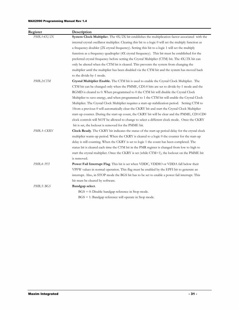
MAX2990 Programming Manual Rev 1.4
Maxim Integrated - 31 -
Register Description PMR.1:4X/2X
System Clock Multiplier. The 4X/2X bit establishes the multiplication factor associated with the
internal crystal oscillator multiplier. Clearing this bit to a logic 0 will set the multiply function as
a frequency doubler (2X crystal frequency). Setting this bit to a logic 1 will set the multiply
function as a frequency quadrupler (4X crystal frequency). This bit must be established for the
preferred crystal frequency before setting the Crystal Multiplier (CTM) bit. The 4X/2X bit can
only be altered when the CTM bit is cleared. This prevents the system from changing the
multiplier until the multiplier has been disabled via the CTM bit and the system has moved back
to the divide-by-1 mode.
PMR.2:CTM Crystal Multiplier Enable. The CTM bit is used to enable the Crystal Clock Multiplier. The
CTM bit can be changed only when the PMME, CD1:0 bits are set to divide-by-1 mode and the
RGMD is cleared to 0. When programmed to 0 the CTM bit will disable the Crystal Clock
Multiplier to save energy, and when programmed to 1 the CTM bit will enable the Crystal Clock
Multiplier. The Crystal Clock Multiplier requires a start-up stabilization period. Setting CTM to
1from a previous 0 will automatically clear the CKRY bit and start the Crystal Clock Multiplier
start-up counter. During the start-up count, the CKRY bit will be clear and the PMME, CD1:CD0
clock controls will NOT be allowed to change to select a different clock mode. Once the CKRY
bit is set, the lockout is removed for the PMME bit.
PMR.3: CKRY Clock Ready. The CKRY bit indicates the status of the start-up period delay for the crystal clock
multiplier warm-up period. When the CKRY is cleared to a logic 0 the counter for the start-up
delay is still counting. When the CKRY is set to logic 1 the count has been completed. The
status bit is cleared each time the CTM bit in the PMR register is changed from low to high to
start the crystal multiplier. Once the CKRY is set (while CTM=1), the lockout on the PMME bit
is removed.
PMR.4: PFI Power Fail Interrupt Flag. This bit is set when VDDC, VDDIO or VDDA fall below their
VPFW values in normal operation. This flag must be enabled by the EPFI bit to generate an
interrupt. Also, in STOP mode the BGS bit has to be set to enable a power fail interrupt. This
bit must be cleared by software.
PMR.5: BGS Bandgap select.
BGS = 0: Disable bandgap reference in Stop mode.
BGS = 1: Bandgap reference will operate in Stop mode.

MAX2990 Programming Manual Rev 1.4
Maxim Integrated - 32 -
Register Description PMR.6-PMR.7:ACTMS AFE Clock Multiplier Select. These bits select the base clock source for prior to the power
management clock divider (clock divide setting is in AFECD[1:0] in CKCN register.
ACTMS[1:0] Base AFE Clock Source
2'b00 AFE Crystal Oscillator
2'b01 PLLA Clock Multiplier Output
2'b10 Pre-PMM System Clock
2'b11 Reserved
When set to ‘01’, this bit selects the crystal multiplier output as the AFE clock once it is ready.
The bit is meaningful only when the clock multiplier is enabled (ACTM=1) and ready for use
(ACKRY=1). The ACTMS bits may be configured to ‘01’ prior to ACKRY=1, in which case the
switch to the multiplier will occur automatically and can be detected by polling the ACKRY bit.
The ACTMS bits are cleared by hardware when the multiplier is disabled (ACTM=0). Setting the
ACTMS bits to '10' selects the system clock (prior to any PMM clock division) as the clock
source. The clock source will be either the system crystal oscillator output, or the output of the
system clock multiplier (PLLS) depending on the setting of the CTM and CTMS bits.
PMR.8:4X/2X-A
AFE Clock Multiplier. The 4X/2X-A bit establishes the multiplication factor associated with the
AFE crystal oscillator multiplier. Clearing this bit to a logic 1 will set the multiply function as
a frequency doubler (2X crystal frequency). Setting this bit to a logic 0 will set the multiply
function as a frequency quadrupler (4X crystal frequency). This bit must be established for the
preferred crystal frequency before setting the Crystal Multiplier (ACTM) bit. The 4X/2X-A bit
can only be altered when the ACTM bit is cleared. This prevents the system from changing the
multiplier until the multiplier has been disabled via the ACTM bit and the system has moved back
to the divide-by-1 mode.
PMR.9:ACTM AFE Multiplier Enable. The ACTM bit is used to enable the AFE Clock Multiplier. The
ACTM bit can be changed only when the AFECD1:0 bits are set to divide-by-1. When
programmed to 0 the ACTM bit will disable the AFE Clock Multiplier to save energy, and
when programmed to 1 the ACTM bit will enable the AFE Clock Multiplier. The AFE Clock
Multiplier requires a start-up stabilization period. Setting ACTM to 1 from a previous 0 will
automatically clear the ACKRY bit and start the AFE Clock Multiplier start-up counter.
During the start-up count, the ACKRY bit will be clear and the AFECD1:0 AFE
clock controls will NOT be allowed to change to select a different clock mode. Once the ACKRY
bit is set the lockout on AFECD1:0 bits will be removed.
PMR.10: ACKRY AFE Clock Ready. The ACKRY bit indicates the status of the start-up period delay for the
AFE crystal clock multiplier warm-up period. When the ACKRY is cleared to a logic 0 the
counter for the start-up delay is still counting. When the ACKRY is set to logic 1 the count has
been completed. The status bit is cleared each time the ACTM bit in the PMR register is changed
from low to high to start the AFE crystal multiplier.
PMR.11: EPFI Enable Power Fail Interrupt. Setting this bit to 1 enables the internal bandgap reference to
generate a power-fail interrupt when VDDIO falls below the VPFW in normal operation. In Stop
mode, the BGS bit has to be set to enable a power-fail interrupt. Clearing this bit to 0 disables the
power fail interrupt.

MAX2990 Programming Manual Rev 1.4
Maxim Integrated - 33 -
Register Description PMR.12: X1BY XTAL1 Oscillator Bypass. Setting this bit to 1 bypasses the amplifier within the system oscillator
circuit to allow an external oscillator to drive a clock directly into the X1 input. Clearing this bit to 0 enables the amplifier and is required for operation with an external crystal between X1 and X2. Note: this bit is automatically set on entry into test mode (TME bit set via JTAG) similar to the DCW bit in the TM register.
PMR.13: X2BY XTAL2 Oscillator Bypass. Setting this bit to 1 bypasses the amplifier within the AFE oscillator circuit to allow an external oscillator to drive a clock directly into the X1 input. Clearing this bit to 0 enables the amplifier and is required for operation with an external crystal between X1 and X2. Note: this bit is automatically set on entry into test mode (TME bit set via JTAG) similar to the DCW bit in the TM register.
PMR.14: X32BY X32k Oscillator Bypass. Setting this bit to 1 bypasses the amplifier within the RTC 32k oscillator circuit to allow an external oscillator to drive a clock directly into the X1 input. Clearing this bit to 0 enables the amplifier and is required for operation with an external crystal between X1 and X2. Note: this bit is automatically set on entry into test mode (TME bit set via JTAG) similar to the DCW bit in the TM register.
PMR.15 Reserved, read returns 0.
I2CCN (09h, 01h)
Initialization:
I2C Control Register (8-bit register)
This register is cleared to 00h on all forms of reset. The I2CSTART and I2CSTOP bits will be resetto ‘0’ when I2CMST=0 or when I2CEN=0.
Read/Write Access: Unrestricted Read. This register can only be written when I2CBUSY=0. I2CMODE bit can only bewritten in master mode (I2CMST=1) and I2CBUSY=0.
I2CCN.0: I2CEN I2C Enable. This bit enables the I2C function. When set to ‘1’, the I2C communication unit isenabled. When cleared to ‘0’, the I2C function is disabled.
I2CCN.1: I2CMST I2C Master Mode Enable. The I2CMST bit functions as a master mode enable bit for the I2Cmodule. When the I2CMST bit is set to ‘1’, the I2C operates as a master. When the I2CMST iscleared to ‘0’, the I2C module operates in slave mode. This bit will automatically be cleared wheneverthe I2C controller receives a slave address match (I2CAMI=1), losses arbitration (I2CALI=1) or ageneral call (I2CGCI=1).
I2CCN.2:I2CMODE I2C Transfer Mode. The transfer mode bit selects the direction of data transfer with respect to themaster. When the I2CMODE bit is set to ‘1’, the master is operating in receiver mode (reading fromslave). When the I2CMODE bit is cleared to ‘0’, the master is operating in transmitter mode (writingto slave).
Note that software writing to this bit is prohibited in slave mode. When operating in master mode,software configures this bit to the desired direction of data transfer. When operating in slave mode,the direction of data transfer is determined by the R/W bit received during the address stage and thisbit will reflect the actual R/W bit value in the current transfer and is set by hardware. Softwarewriting to this bit in slave mode is ignored.
I2CCN.3:I2CEA I2C Extended Address Enabled. This bit selects the addressing mode used during the addressphase. When set to ‘1’, the I2C will generate/receive a 10-bit slave address in the address stage.When cleared to ‘0’, a 7-bit address will be used in the address stage.
I2CCN.4:I2CSTRS I2C Clock Stretch Select. Setting this bit to ‘1’ will enable clock stretching after the falling edge ofthe 8th clock cycle. Clearing this bit to ‘0’ will enable clock stretching after the falling edge of the 9th
clock cycle. This bit has no effect when clock stretching is disabled (I2CSTREN=0).
I2CCN.5:I2CACK I2C Data Acknowledge Bit. This bit selects the acknowledge bit returned by the I2C Controllerwhile acting as a receiver. Setting this bit to ‘1’ will generate a NACK (leaving SDA high). Clearingthe I2CACK bit to ‘0’ will generate an ACK (pulling SDA LOW) during the acknowledgement cycle.This bit will remain set unless cleared by software writing a ‘0’.

MAX2990 Programming Manual Rev 1.4
Maxim Integrated - 34 -
Register Description I2CCN.6:I2CSTART I2C START Enable. Setting this bit will automatically generate a START condition when the bus is
free or a repeated START condition during a transfer where the I2C module is operating as themaster. This bit will automatically be self-cleared to ‘0’ after the START condition has beengenerated. If the I2C START interrupt is enabled, a START condition will generate an interrupt tothe CPU.
In master mode, setting this bit will also start the timeout timer if enabled. If the timeout timerexpires before the START condition can be generated, a timeout interrupt will be generated to theCPU if enabled. The I2CSTART bit will also be cleared to ‘0’ by the timeout event.
Note that this bit has no effect when the I2C is operating in slave mode (I2CMST=0) and will bereset to ‘0’ when I2CMST =0 or I2CEN=0.
I2CCN.7:I2CSTOP I2C STOP Enable. Setting this bit to ‘1’ will generate a STOP condition. This bit will automatically be self-cleared to ‘0’ after the STOP condition has been generated.
Note that this bit has no effect when the I2C is operating in slave mode (I2CMST=0) and will be reset to ‘0’ when I2CMST=0 or I2CEN=0.
I2CCK (0Ah, 01h)
Initialization:
Read/Write Access:
I2C Clock Control Register (16-bit register)
This register is cleared to 0204h on all forms of reset.
Unrestricted Read. Write to this register is allowed only when I2CBUSY=0. This register has nofunction when operating in slave mode and the clock generation circuitry should be disabled.
I2CCK.7 – 0:
I2CCKL[7-0]
I2C Clock Low Bits 7:0. These bits define the I2C SCL low period in number of system clock, withbit 7 as the most significant bit. The duration of SCL low time is calculated using the followingequation:
I2C Low Time Period = System Clock * (I2CCKL[7:0]+1)
I2CCK.15 – 8:
I2CCKH[7-0]
I2C Clock High Bits 7:0. These bits define the I2C SCL high period in number of system clock,with bit 7 as the most significant bit. The duration of SCL high time is calculated using the followingequation:
I2C High Time Period = System Clock * (I2CCKH[7:0]+1)
I2CTO (0Bh, 01h)
Initialization:
Read/Write Access:
I2C Timeout Register (8-bit register)
This register is cleared to 00h on all forms of reset.
Unrestricted read/write access.
I2CTO.7 – 0 I2C Timeout Register Bits 7:0. This register is used only in master mode. This register determinesthe number of I2C Bit Period (SCL High + SCL Low) the I2C master will wait for SCL to go high.The timeout timer will reset to 0 and start to count after the I2CSTART bit is set or every time theSCL goes low. When cleared to 00h, the timeout function is disabled and the I2C will wait for SCL togo high indefinitely during a transmission. When set to any other values, the I2C will wait until thetimeout expires and set the I2CTOI flag.
I2C Timeout = I2C Bit Rate * (I2CTO[7:0] + 1)
Note that these bits have no effect when the I2C module is operating in slave mode (I2CMST=0).When operating in slave mode, SCL is controlled by an external master.
I2CSLA (0Ch, 01h)
Initialization:
Read/Write Access:
I2C Slave Address Register (16-bit register)
This register is cleared to 0000h on all forms of resets
Unrestricted read/write access
I2CSLA.9 – 0 I2C Slave Address Register Bits 9:0. These address bits contain the address of the I2C device. When a match to this address is detected, the I2C controller will automatically acknowledge the transmitter with the I2CACK bit value if the I2C module is enabled (I2CEN=1). The I2CAMI flag will be set to ‘1’ and the I2CMST bit will be cleared to ‘0’. An interrupt will be generated to the CPU if enabled.
I2CSLA.15 – 10 Reserved. Read returns zero.
TM2 (0Dh, 01h)
Initialization:
Read/Write Access:
Test Mode Register 2
All bits are cleared to 0 after a power-on reset or a Test-Logic-Reset TAP state.
Unrestricted read/write for bits 11:0 when TME is set. No CPU access when it is not

MAX2990 Programming Manual Rev 1.4
Maxim Integrated - 35 -
Register Description TM2.0-TM2.5: TRIM
Trim Word. These bits are the trim value to be used when accessing the internal trim register selected by the TSEL bits (TM2[7:6]). When in test mode, a write to this register updates the internal trim register for the selected function to be trimmed. When accessed for read, these bits reflect the actual value of the internal trim register that is selected by TSEL. All trim registers are updated from the flash information block on POR, these bits allow for rapid override of the POR values in the register to find the optimum trim value for the function being tested. This value should then be written to the appropriate field of the flash information block. When TME is not set, reads of this register return zero and writes to this register are ignored.
TM2.6-TM2.7:TSEL Trim Select. These bits select one of the four functions whose trim values are being accessed by the TRIM bits of SFR TM2[5:0]. A write to this register of the decode in the table below and a trim valuein TM2[5:0] will write the new trim value into the trim bit register for that function. A read of theTM2 register will reflect the actual trim values currently loaded into the trim register for the function defined in the TSEL decode table. If TME is not set, reads of this register return zero and writes areignored.
TSEL[1:0] Function Selected for Trim
2'b00 PLLA (AFE PLL)
2'b01 PLLS (System PLL)
2'b10 Bandgap
2'b11 1MHz Flash Oscillator
TM2.8-TM2.9: XT1
XTAL1 Test Bits. These two bits are used to test if the XTAL1 (system) oscillator is functioning as expected.
TM2.10-TM2.11: XT2
XTAL2 Test Bits. These two bits are used to test if the XTAL2 (AFE) oscillator is functioning as expected.
TM2.12-TM2.15 Reserved, read returns 0.
FCNTL (0Eh, 01h)
Initialization:
Read/Write Access:
Flash Memory Control Register
This register is cleared to 80h on all forms of reset.
Unrestricted read, bits 2-0 write accessible only by Utility ROM or logical data memory (This register is not accessible by program code inside the Flash memory because of the rule governing the pseudo Von Neumann mapping. Access is blocked by hardware.). Also, write access to FCNTL is prohibited when FBUSY is 0.
FCNTL.0: FC0
FCNTL.1: FC1
FCNTL.2: FC2
Flash Command Bit 0
Flash Command Bit 1
Flash Command Bit 2
These Flash Command bits provide the following commands for Flash operations:
FC2 FC1 FC0 Flash Commands
0 0 0 Read Mode (Default)
0 0 1 Verify Information Block
0 1 0 Write Information Block
0 1 1 Write Main Memory Block
1 0 0 Erase Information Block
1 0 1 Page Erase of Main Memory Block
1 1 0 Mass Erase of Main Memory Block
The MMU supports only the above commands, other settings are reserved. Using any reserved command results no operation.
FCNTL.6 – FCNTL.3 Reserved, read return 0.
FCNTL.7: FBUSY
Flash Busy. This busy flag will be cleared to a logic 0 to indicate the start of an erase/program operation by the MMU immediately following the command sequence. It will be hold low until the end of the operation. Set/reset of this flag is synchronized with the system clock.
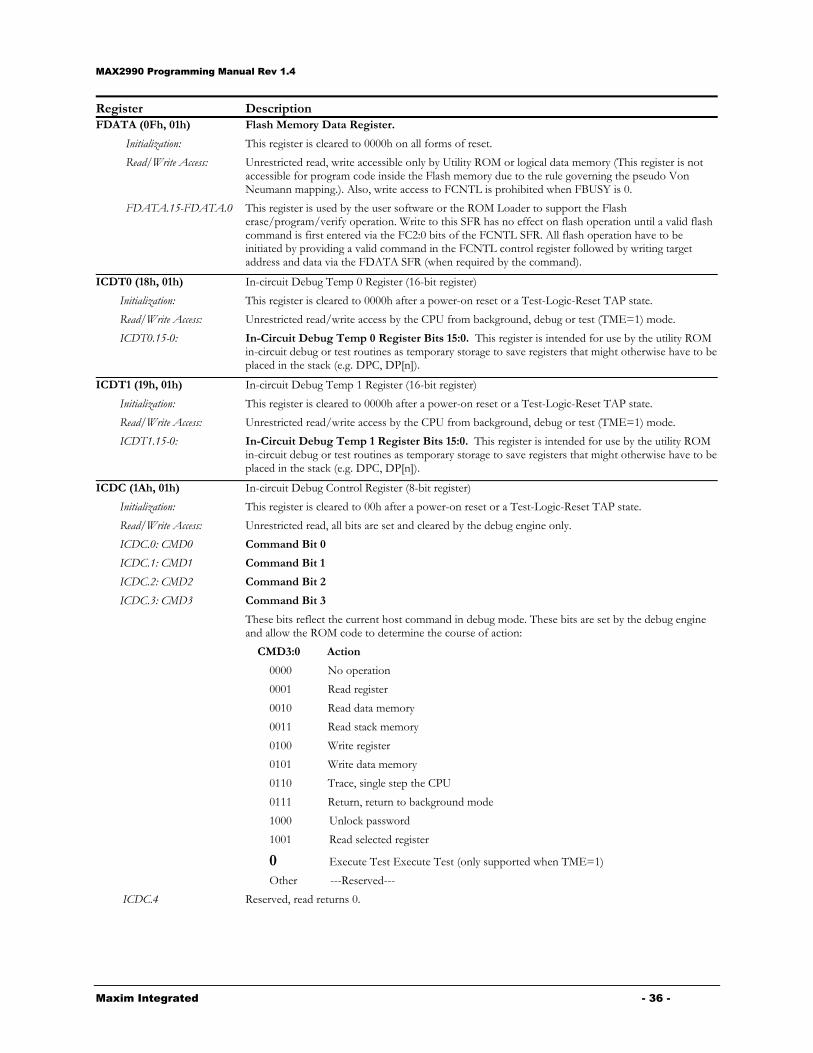
MAX2990 Programming Manual Rev 1.4
Maxim Integrated - 36 -
Register Description FDATA (0Fh, 01h)
Initialization:
Read/Write Access:
Flash Memory Data Register.
This register is cleared to 0000h on all forms of reset.
Unrestricted read, write accessible only by Utility ROM or logical data memory (This register is not accessible for program code inside the Flash memory due to the rule governing the pseudo Von Neumann mapping.). Also, write access to FCNTL is prohibited when FBUSY is 0.
FDATA.15-FDATA.0
This register is used by the user software or the ROM Loader to support the Flash erase/program/verify operation. Write to this SFR has no effect on flash operation until a valid flash command is first entered via the FC2:0 bits of the FCNTL SFR. All flash operation have to be initiated by providing a valid command in the FCNTL control register followed by writing target address and data via the FDATA SFR (when required by the command).
ICDT0 (18h, 01h)
Initialization:
Read/Write Access:
ICDT0.15-0:
In-circuit Debug Temp 0 Register (16-bit register)
This register is cleared to 0000h after a power-on reset or a Test-Logic-Reset TAP state.
Unrestricted read/write access by the CPU from background, debug or test (TME=1) mode.
In-Circuit Debug Temp 0 Register Bits 15:0. This register is intended for use by the utility ROM in-circuit debug or test routines as temporary storage to save registers that might otherwise have to be placed in the stack (e.g. DPC, DP[n]).
ICDT1 (19h, 01h)
Initialization:
Read/Write Access:
ICDT1.15-0:
In-circuit Debug Temp 1 Register (16-bit register)
This register is cleared to 0000h after a power-on reset or a Test-Logic-Reset TAP state.
Unrestricted read/write access by the CPU from background, debug or test (TME=1) mode.
In-Circuit Debug Temp 1 Register Bits 15:0. This register is intended for use by the utility ROM in-circuit debug or test routines as temporary storage to save registers that might otherwise have to be placed in the stack (e.g. DPC, DP[n]).
ICDC (1Ah, 01h)
Initialization:
Read/Write Access:
In-circuit Debug Control Register (8-bit register)
This register is cleared to 00h after a power-on reset or a Test-Logic-Reset TAP state.
Unrestricted read, all bits are set and cleared by the debug engine only.
ICDC.0: CMD0
ICDC.1: CMD1
ICDC.2: CMD2
ICDC.3: CMD3
Command Bit 0
Command Bit 1
Command Bit 2
Command Bit 3
These bits reflect the current host command in debug mode. These bits are set by the debug engine and allow the ROM code to determine the course of action:
CMD3:0 Action
0000 No operation
0001 Read register
0010 Read data memory
0011 Read stack memory
0100 Write register
0101 Write data memory
0110 Trace, single step the CPU
0111 Return, return to background mode
1000 Unlock password
1001 Read selected register
0 Execute Test Execute Test (only supported when TME=1)
Other ---Reserved---
ICDC.4 Reserved, read returns 0.

MAX2990 Programming Manual Rev 1.4
Maxim Integrated - 37 -
Register Description ICDC.5: REGE
Break on Register Enable. The REGE bit is used to enable the break on register function. When REGE bit is set to 1, BP4 and BP 5 are used as the breakpoint for register content. A break occurs when the content of BP4 is matched with the destination address of the current instruction. For BP5, a break occurs only on a selected data pattern for a selected destination register addressed by BP5, the data pattern is determined by the contents in the ICDA and ICDD register. The REGE bit alone does not enable register breakpoint; it is simple changes the manner in which BP4 and BP5 are used. The DME bit still must be configured to logic 1 in order for any breakpoint to occur. This bit has no meaning for the ROM code.
ICDC.6:TE Timer Enable. The TE bit is used to enable the internal timer function in debug mode. Setting thisbit to 1 allows the internal timers to continue their normal function. When this bit is cleared to 0, theinternal timer function will be automatically disabled in debug mode, including the watchdog timer.This bit must be set before entering the debug mode. This bit has no meaning for the ROM code.
ICDC.7: DME
Debug Mode Enable. When this bit is cleared to 0, background mode commands may be executed but breakpoints are disabled. When this bit is set to 1, breakpoints are enabled while background mode commands still may be entered. This bit is only be set or cleared from background mode. This bit has no meaning for the ROM code.
ICDF (1Bh, 01h)
Initialization:
Read/Write Access:
In-circuit Debug Flag Register (8-bit register)
This register is cleared to 00h after a power-on reset or a Test-Logic-Reset TAP state.
Unrestricted read, only bits 3:0 is writable by the CPU.
ICDF.0: TXC
Serial Transfer Complete. This bit is set by hardware at the end of a transfer cycle at the TAP communication link. The TXC helps the debug engine to recognize host requests, either command or data. This bit is normally set by ROM code to signify/request sending or receiving data; the TXC must be cleared by the debug engine once set. CPU writes to the TXC bit will result in clearing of the JTAG PSS1:0 bits.
ICDF.1: SPE
System Program Enable. The SPE bit is used for In-System programming support and its logical state, when read by the CPU, I reflects the logical-OR of the SPE bit that is write accessible by the CPU and the SPE bit of the System Programming Buffer (SPB) Register in the TAP Module (which is accessible via JTAG). The logical state of this bit determines the program flow after a reset. When it is set to logic 1, In-System programming will be executed by the Utility ROM. When it is cleared to 0, execution will be transferred to user code. This bit allows read/write access by the CPU and is cleared to 0 only on a power-on reset or Test-Logic-Reset. The JTAG SPE bit will be cleared by hardware when the ROD bit is set. CPU writes to the SPE bit will result in clearing of the JTAG PSS1:0 bits.
ICDF.2: PSS0
Programming Source Select Bit.
This bit is used to select a programming interface during In-System programming when SPE is set to logic 1, otherwise, the logic values of these bits have no meaning:
PSS0 Source Selection
0 JTAG
1 UART
The logical states of these bits, when read by the CPU, reflect the logical-OR of the PSS bits that are write accessible by the CPU and those in the System Programming Buffer (SPB) Register of the TAP module (which are accessible via JTAG). These bits are read/write accessible for the CPU and are cleared to 0 by a power-on reset or Test-Logic-Reset. CPU writes to the PSS bits will result in clearing of the JTAG PSS1:0 bits.
ICDF.4:PSPE PROG SPE: This read only bit will be forced to 1 when the PROG pin is detected with a low
state for 4 consecutive system clocks. The setting of the PSPE will cause a reset. The reset state
will be maintained for 4 system clock cycles. Once the reset is removed, the processor will
resume execution at address 8000h. Note that the PSPE can only be cleared by a POR or the
setting of ROD bit. When the PSPE bit is already set, PROG assertion will not cause additional
reset. The purpose of the PROG pin is to signal a UART programming request without going
through the JTAG interface.
ICDF.7-ICDF.3 Reserved, read returns 0.

MAX2990 Programming Manual Rev 1.4
Maxim Integrated - 38 -
Register Description ICDB (1Ch, 01h)
Initialization:
Read/Write Access:
ICDB.7 – ICDB.0
In-circuit Debug Buffer Register (8-bit register)
This register is cleared to 00h after a power-on reset or a Test-Logic-Reset TAP state.
Unrestricted read/write by CPU
In-Circuit Debug Buffer Bits 7:0. ICDB serves as the parallel holding buffer for the debug shift register of the TAP. Data is read from or written to ICDB for serial communication between the debug function and the external host. This register is mapped to the SFR space for read/write access by the CPU.
ICDA (1Dh, 01h)
Initialization:
Read/Write Access:
ICDA.15 – ICDA.0
In-circuit Debug Address Register (16-bit register)
This register is cleared to FFFFh after a power-on reset or a Test-Logic-Reset TAP state.
Unrestricted read by CPU
In-Circuit Debug Address Bits 15:0. This register serves as the address register for the debug engine to store a specific location for ROM code execution. This register is also used by the debug engine as a mask register to mask out don’t care bits in the ICDD register when BP5 is used as a register breakpoint. When a bit in this register is set to 1, the corresponding bit location in the ICDD register will be compared to the updating destination data to determine if a break should be generated. When a bit in this register is cleared, the corresponding bit in the ICDD register becomes a don’t care and is not compared against the updating data. When all bits in this register are cleared, any updated data pattern will cause a break when the BP5 register matches the destination register address of the current instruction.
ICDD (1Eh, 01h)
Initialization:
Read/Write Access:
ICDD.15 – ICDD.0
In-circuit Debug Data Register (16-bit register)
This register is cleared to 0000h after a power-on reset or a Test-Logic-Reset TAP state.
Unrestricted read by CPU
In-Circuit Debug Data Bits 15:0. This register serves as the data/count register for the debug engine to store data or read count for ROM code execution. This register is also used by the debug engine as a data register for content matching when BP5 is used as a register breakpoint. In this case, only data bits in this register with their corresponding mask bits in the ICDA register set will be compared with the updated destination data to determine if a break should be generated.
TM (1Fh, 01h)
Initialization:
Read/Write Access:
Test Mode Register (16-bit register)
All bits are cleared to 0 after a power-on reset or a Test-Logic-Reset TAP state, except the SRT
and DCW bits are cleared by power-on reset only.
Unrestricted read/write for bits 15:1 when TME is set, bits 0 are read only for the CPU.
TM.0: TME
Test Mode Enable. This bit is used to enable the test state machine and its logical state is always reflected the logical state of the TME bit of the Test Data Buffer in the TAP module. This bit is read only by the CPU.
TM.1: Reserved, read returns 0.
TM.2: CKT
Clock Test Enable. Setting this bit to a logic 1 enables the test functions in the clock switch over circuitry. In this mode, the micro will always be clocked from the divide by 1 crystal clock input regardless of the state of CD1 and CD0 or any of the other clock source select inputs. The CKT is automatically set to 1 when the test mode is enabled (TME=1).
TM.3: SRT
Switch Reset Trip Point Voltage. When this bit is cleared to 0 the Reset trip point occurs at its normal voltage in relation to use of the bandgap and Vcc input. The Vccmin value is approximately TBD volts. When this bit is set to 1, the Reset trip point is referenced to ground instead of the bandgap. The SRT is cleared by a power-on reset or software once set.
TM.4: DOFF Stop Watchdog Count. Setting this bit to 1 disables the clock to the watchdog. Clearing this bit to 0 allows the watchdog to count.
TM.5: IDDQ IDDQ Test. Setting this bit to 1 will put the device in stop mode, essentially shut off all current sources for IDDQ test. Clearing this bit to 0 allows the device to resume it normal function.

MAX2990 Programming Manual Rev 1.4
Maxim Integrated - 39 -
Register Description TM.6: DCW
Disable Crystal Warm-Up. This bit allows the tester to disable the crystal warm-up circuitry for power-up during device test. Setting this bit to logic 1 bypasses the crystal warm-up period. Clearing this bit to 0 the device will cycle through the normal crystal warm-up time before releasing the chip reset. The DCW is automatically set to 1 when the test mode is enabled (TME=1) which allows to by-pass the warm-up period when entering test mode. This warm up period bypass applies to both crystal oscillators, the system oscillator and the AFE oscillator. The DCW is cleared by a power-on reset or software once set.
TM.7-TM8: COUT
System Clock Output Enable. These bits control what clock is output on port pin P2.3 in test mode. The selected clock is sent out, post prescaling, divided by two to reduce the switching rate of the package pin. This function is only available when TME is set. The clock source selected by these bits are shown below.
COUT[1:0] Selected Clock
2'b00 No clocks selected (function disabled
2'b01 System (MCU) Clock Source
2'b10 PHY Clock Source
2'b11 AFE Clock Source
TM.9: DBPIDLE
Debug PHY IDLE. Setting this bit to a logic 1 will force the PHY TX path into a debug/test mode where in it repeats back to back 'P' symbols for as long as the mode is set.
TM.10: PLLTRIM
PLL Trim Mode. Setting this bit to a logic 1 will output the currents required for trimming both PLLs on port pins. PLLA will output its trim current on P3.0, and PLLB will output on P0.7.
TM.11: BGTRIM
Bandgap Trim Mode. Setting this bit to a logic 1 will output the current required for trimming the Bandgap on P1.0.
TM.12-TM14: RCOUT Raw Clock Output Enable. These bits control raw clock output on the specified port pins. These clock sources are output on the pins prior to any conditioning and irrespective of any clock divide modes or other settings.
RCOUT[2:0] Selected Clock Output Pin 3'b000 No clocks selected (function
disabled) -
3'b001 No clocks selected (function disabled)
3'b010 XTALS P1.0 3'b011 PLLS P1.0 3’b100 XTALA P3.0 3’b101 PLLA P3.0 3’b110 1MHz Ring P0.3 3’b111 32kHz P0.3
TM.15 Reserved, read returns 0.
DMINT (00h, 02h)
Initialization:
Read/Write Access:
Data Manager Interrupt Control Register
The Data Manager Interrupt Control Register is cleared to 0000h on all forms of reset.
Unrestricted read/write.
DMINT.0: PYTXIF
PHY Tx Interrupt Flag. When set, this bit indicates the last bit of a frame of data has been transferred to the AFE. This bit must be cleared by software. There are three sources of a data transfer to the AFE, the OSTART bit in the DMCN register, the TXRetran and ACKSTART bits in the PCR register will all start a transmit operation and will trigger this interrupt if enabled.
DMINT.1: DMTXIF
Data Manager Tx Interrupt Flag. When set, this bit indicates the last byte of a complete frame of data has been transferred from the buffer manager to the PHY. This bit must be cleared by software. There are three ways to start a transmit, the OSTART bit in the DMCN register, the TXRetran and ACKSTART bits in the PCR register. Of these three, only the OSTART will cause a transfer of data between the packet memory and the PHY, and only the OSTART based transmission will cause a DMTXIF interrupt on completion.

MAX2990 Programming Manual Rev 1.4
Maxim Integrated - 40 -
Register Description DMINT.2: PYRXIF
PHY Rx Interrupt Flag. When set, this bit indicates the last bit of a frame of data has been decoded by the PHY. This bit must be cleared by software.
DMINT.3: DMRXIF
Data Manager Rx Interrupt Flag. When set, this bit indicates the last byte of a complete frame of data has been transferred from the PHY to the buffer and is ready for MAC processing. This bit must be cleared by software.
DMINT.4: DESIF
DES Interrupt Flag. When set, this bit indicates the currently running DES operation has completed. This includes the two cycles required to transfer the CRC32 value to the buffer memory. This bit must be cleared by software.
DMINT.5: PCSIF
PHY Carrier Sense Interrupt Flag. When set, this bit indicates the PHY has detected a carrier. This bit must be cleared by software.
DMINT.6: FDIF
Frame Detect Interrupt Flag. When set, this bit indicates the frame synchronizer has detected a valid frame. This bit must be cleared by software.
DMINT.7: RXOVRIF RX Overflow Interrupt Flag. If enabled by RXOVRIE, this bit indicates an RX overflow condition has been detected and the frame of data in the FEC has been automatically flushed to prevent a lock up condition. If not enabled, no flush will be performed on overflow and firmware must handle the condition manually.
DMINT.8: PYTXIE
PHY Tx Interrupt Enable. When set, this bit enables the interrupt triggered by the last bit of data being transferred to the AFE.
DMINT.9: DMTXIE
Data Manager Tx Interrupt Enable. When set, this bit enables the interrupt triggered by the last byte of a complete frame of data being transferred from the buffer manager to the PHY.
DMINT.10: PYRXIE
PHY Rx Interrupt Enable. When set, this bit enables the interrupt triggered by the last bit of a frame of data having been decoded by the PHY.
DMINT.11: DMRXIE
Data Manager Rx Interrupt Enable. When set, this bit enables the interrupt triggered by the last byte of a complete frame of data having been transferred from the PHY to the buffer.
DMINT.12: DESIE
DES Interrupt Enable. When set, this bit enables the interrupt triggered by the completion of the currently running DES operation.
DMINT.13: PCSIE
PHY Carrier Sense Interrupt Enable. When set, this bit enables the interrupt triggered by the PHY carrier sense detect.
DMINT.14: FDIE
Frame Detect Interrupt Enable. When set, this bit enables the interrupt triggered by the frame synchronizer frame detect.
DMINT.15: RXOVRIE RX Overflow Interrupt Enable. When set, this bit enables circuitry that will detect the presence of a new incoming frame (FRMRX bit in PSR) and monitor the status of the FECDATA bit. If the FECDATA bit remains set when the FRMRX bit is asserted, an overflow condition is detected, the RXOVRIF flag is set and the frame in the FEC is automatically flushed to prevent a lock up condition.
DESCN (01h, 02h)
Initialization:
Read/Write Access:
DES Control Register
The DES Control Register is cleared to 1Ch on all forms of reset.
Unrestricted read/write to bits 0 through 3. Bit 4 is read only.
DESCN.0: START
START bit. When set, this bit starts a DES operation using the configuration currently set in the DES/CRC32 registers. The DES engine reads data to be encrypted or decrypted (set with the MODE bit) from the address pointed to by the DESAD register. Data is written back over the source data in the buffer memory when the operation is complete and the next block of data is processed until the number of blocks indicated by the DESCNT register is done. The CRC32 checksum for the whole block of data is automatically appended to the processed data. This bit also resets the CRC32 register to it’s seed value of FFFFFFFFh. This bit is cleared by hardware when the DES operation has started.
DESCN.1: MODE MODE bit. This bit sets the mode (0 = decryption, 1 = encryption) for DES operation. it is set and cleared by software only.

MAX2990 Programming Manual Rev 1.4
Maxim Integrated - 41 -
Register Description DESCN.2-DESCN.3:
DOP
DES Operation bits. These bits set the operating mode for the DES block.
DOP[1:0](DESCN[3:2]) DES/CRC32 Operating Mode
00 DES and CRC32 disabled
01 CRC32 operation only, no DES
10 DES operation only, no CRC32
11 DES and CRC32 enabled
If the DES and CRC32 are both disabled, the START bit has no meaning and should be ignored. DES and CRC32 both enabled will require the most processing time, as there is full read and write back of the data being operated on, and a write of the CRC32 result at the end of the operation. DES only mode, will require slightly less operation time, as the write of the CRC checksum does not have to be performed at the end of the operation. CRC32 only mode will require the least processing time, as the data in the packet memory does not need to be written back to, as with a encrypt or decrypt operation.
DESCN.4: DONE DONE bit. This bit indicates when the DES is busy or idle. This bit goes low when a DES operation is running and is high when there is no operation running.
DESCN.5 –DESCN.7 Reserved, read returns 0.
DESAD (02h, 02h)
Initialization:
Read/Write Access:
DESAD.0 – DESAD.15
DES Address Register
The DES Address Register is cleared to 0000h on all forms of reset.
Unrestricted read/write.
This register defines the starting address of the block of data in the buffer memory to be operated on. The DES block automatically fetches the number of blocks defined by DESCNT starting at this address to encrypt or decrypt. Note that this address is the logical address that the MCU used to store this data in the buffer memory. Logical to physical address mapping will be done in the Buffer Manager. Also note that this is a word address only. The Buffer Manager must be configured to use word mode for the interface to the DES block, and therefore, this register should always be written with word addresses.
DESCNT (03h, 02h)
Initialization:
Read/Write Access:
DESCNT.0–DESCNT.15
DES Block Count Register
The DES Block Count Register is cleared to 00h on all forms of reset.
Unrestricted read/write.
This register defines the number of 64 bit cypher blocks to be operated on starting at DESAD in the buffer memory. It is the MAC firmwares responsibility to ensure there are an integer number of complete 64 bit cypher blocks stored in the memory. If this is a block to be encrypted and CRC32 is enabled, this count does not include the extra cipher block needed to store the encrypted CRC result.
DESKEY (04h, 02h)
Initialization:
Read/Write Access:
DESKEY.0-DESKEY.15
DES Key Register
The Data Key Register is cleared to 0000000000000000h on all forms of reset.
Unrestricted read/write.
This register address serves as the access point for the 64 bit DES key register. To initialize the whole key register, four consecutive 16 bit writes are done on this register. This first write sets the low word, the second sets the 2nd word, the third write sets the 3rd word, and the fourth write sets the highest word. All forms of reset will clear all 64 bits.
CRC32 (05h, 02h)
Initialization:
Read/Write Access:
CRC32.0-CRC32.15
DES CRC32 Register
The DES CRC32 Register is cleared to 00000000h on all forms of reset and the start of a new DES operation (DESCN register START bit set)
Unrestricted read, no write is allowed.
This register address serves as the access point for the 32 bit CRC32 register. This register reflects the contents of the actual CRC32 LFSR shift register. The CRC32 register is automatically set to the appropriate seed value of all zeros when a new DES operation is started. It requires two consecutive reads to access the whole 32 bit long word. Starting a CRC32 operation will automatically set the internal read pointer to the low word. Subsequent reads will toggle the internal read pointer between the low word and the high word. Note: these bits is meant for diagnostic use only, it is not needed for normal DES operation based CRC32 operation.
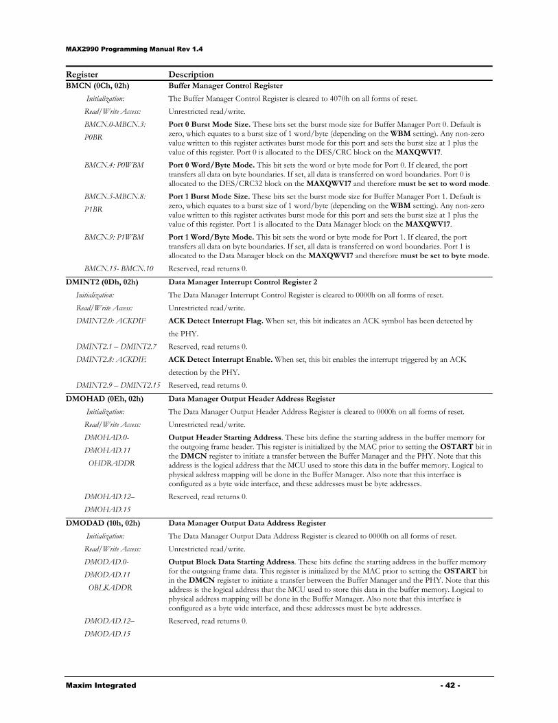
MAX2990 Programming Manual Rev 1.4
Maxim Integrated - 42 -
Register Description BMCN (0Ch, 02h)
Initialization:
Read/Write Access:
Buffer Manager Control Register
The Buffer Manager Control Register is cleared to 4070h on all forms of reset.
Unrestricted read/write.
BMCN.0-MBCN.3:
P0BR
Port 0 Burst Mode Size. These bits set the burst mode size for Buffer Manager Port 0. Default is zero, which equates to a burst size of 1 word/byte (depending on the WBM setting). Any non-zero value written to this register activates burst mode for this port and sets the burst size at 1 plus the value of this register. Port 0 is allocated to the DES/CRC block on the MAXQWV17.
BMCN.4: P0WBM
Port 0 Word/Byte Mode. This bit sets the word or byte mode for Port 0. If cleared, the port transfers all data on byte boundaries. If set, all data is transferred on word boundaries. Port 0 is allocated to the DES/CRC32 block on the MAXQWV17 and therefore must be set to word mode.
BMCN.5-MBCN.8:
P1BR
Port 1 Burst Mode Size. These bits set the burst mode size for Buffer Manager Port 1. Default is zero, which equates to a burst size of 1 word/byte (depending on the WBM setting). Any non-zero value written to this register activates burst mode for this port and sets the burst size at 1 plus the value of this register. Port 1 is allocated to the Data Manager block on the MAXQWV17.
BMCN.9: P1WBM
Port 1 Word/Byte Mode. This bit sets the word or byte mode for Port 1. If cleared, the port transfers all data on byte boundaries. If set, all data is transferred on word boundaries. Port 1 is allocated to the Data Manager block on the MAXQWV17 and therefore must be set to byte mode.
BMCN.15- BMCN.10 Reserved, read returns 0.
DMINT2 (0Dh, 02h)
Initialization:
Read/Write Access:
DMINT2.0: ACKDIF
DMINT2.1 – DMINT2.7
DMINT2.8: ACKDIE
DMINT2.9 – DMINT2.15
Data Manager Interrupt Control Register 2
The Data Manager Interrupt Control Register is cleared to 0000h on all forms of reset.
Unrestricted read/write.
ACK Detect Interrupt Flag. When set, this bit indicates an ACK symbol has been detected by
the PHY.
Reserved, read returns 0.
ACK Detect Interrupt Enable. When set, this bit enables the interrupt triggered by an ACK
detection by the PHY.
Reserved, read returns 0.
DMOHAD (0Eh, 02h)
Initialization:
Read/Write Access:
Data Manager Output Header Address Register
The Data Manager Output Header Address Register is cleared to 0000h on all forms of reset.
Unrestricted read/write.
DMOHAD.0-
DMOHAD.11
OHDRADDR
Output Header Starting Address. These bits define the starting address in the buffer memory for the outgoing frame header. This register is initialized by the MAC prior to setting the OSTART bit in the DMCN register to initiate a transfer between the Buffer Manager and the PHY. Note that this address is the logical address that the MCU used to store this data in the buffer memory. Logical to physical address mapping will be done in the Buffer Manager. Also note that this interface is configured as a byte wide interface, and these addresses must be byte addresses.
DMOHAD.12–
DMOHAD.15
Reserved, read returns 0.
DMODAD (10h, 02h)
Initialization:
Read/Write Access:
Data Manager Output Data Address Register
The Data Manager Output Data Address Register is cleared to 0000h on all forms of reset.
Unrestricted read/write.
DMODAD.0-
DMODAD.11
OBLKADDR
Output Block Data Starting Address. These bits define the starting address in the buffer memory for the outgoing frame data. This register is initialized by the MAC prior to setting the OSTART bit in the DMCN register to initiate a transfer between the Buffer Manager and the PHY. Note that this address is the logical address that the MCU used to store this data in the buffer memory. Logical to physical address mapping will be done in the Buffer Manager. Also note that this interface is configured as a byte wide interface, and these addresses must be byte addresses.
DMODAD.12–
DMODAD.15
Reserved, read returns 0.
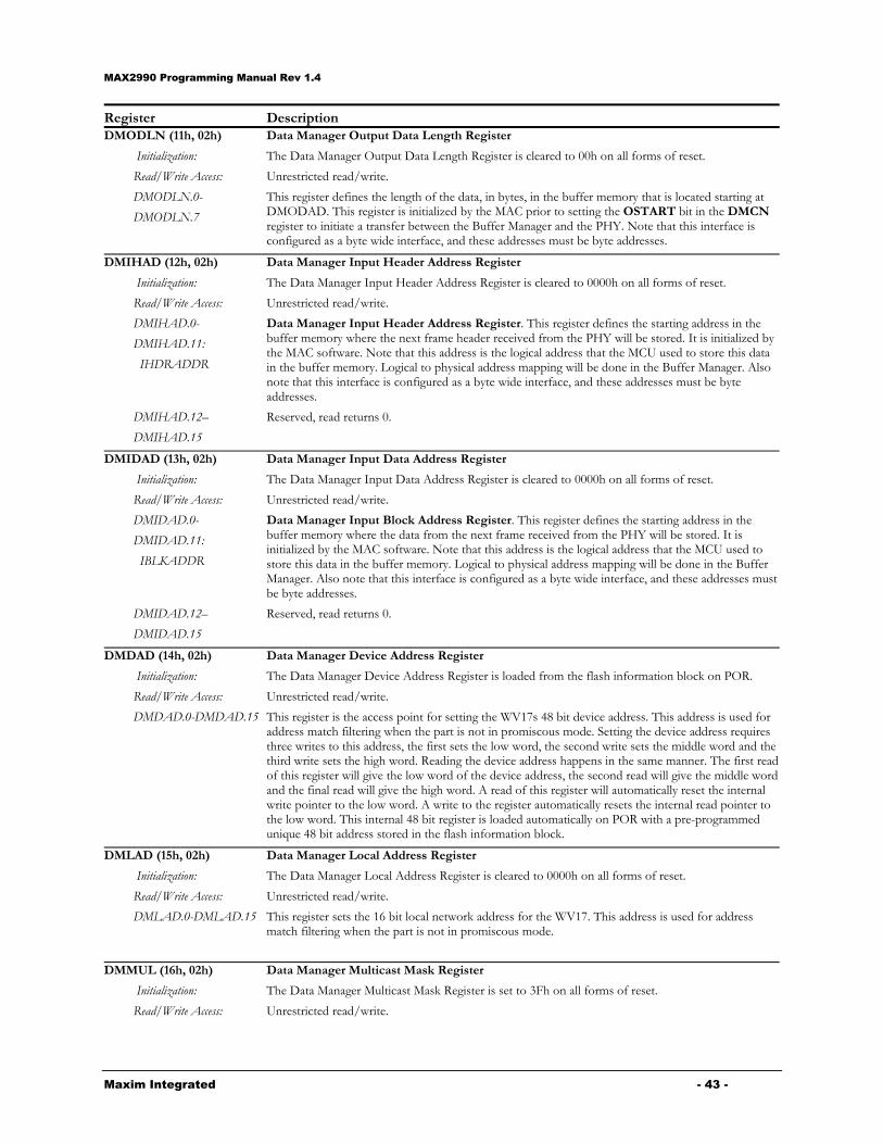
MAX2990 Programming Manual Rev 1.4
Maxim Integrated - 43 -
Register Description DMODLN (11h, 02h)
Initialization:
Read/Write Access:
DMODLN.0-
DMODLN.7
Data Manager Output Data Length Register
The Data Manager Output Data Length Register is cleared to 00h on all forms of reset.
Unrestricted read/write.
This register defines the length of the data, in bytes, in the buffer memory that is located starting at DMODAD. This register is initialized by the MAC prior to setting the OSTART bit in the DMCN register to initiate a transfer between the Buffer Manager and the PHY. Note that this interface is configured as a byte wide interface, and these addresses must be byte addresses.
DMIHAD (12h, 02h)
Initialization:
Read/Write Access:
Data Manager Input Header Address Register
The Data Manager Input Header Address Register is cleared to 0000h on all forms of reset.
Unrestricted read/write.
DMIHAD.0-
DMIHAD.11:
IHDRADDR
Data Manager Input Header Address Register. This register defines the starting address in the buffer memory where the next frame header received from the PHY will be stored. It is initialized by the MAC software. Note that this address is the logical address that the MCU used to store this data in the buffer memory. Logical to physical address mapping will be done in the Buffer Manager. Also note that this interface is configured as a byte wide interface, and these addresses must be byte addresses.
DMIHAD.12–
DMIHAD.15
Reserved, read returns 0.
DMIDAD (13h, 02h)
Initialization:
Read/Write Access:
Data Manager Input Data Address Register
The Data Manager Input Data Address Register is cleared to 0000h on all forms of reset.
Unrestricted read/write.
DMIDAD.0-
DMIDAD.11:
IBLKADDR
Data Manager Input Block Address Register. This register defines the starting address in the buffer memory where the data from the next frame received from the PHY will be stored. It is initialized by the MAC software. Note that this address is the logical address that the MCU used to store this data in the buffer memory. Logical to physical address mapping will be done in the Buffer Manager. Also note that this interface is configured as a byte wide interface, and these addresses must be byte addresses.
DMIDAD.12–
DMIDAD.15
Reserved, read returns 0.
DMDAD (14h, 02h)
Initialization:
Read/Write Access:
DMDAD.0-DMDAD.15
Data Manager Device Address Register
The Data Manager Device Address Register is loaded from the flash information block on POR.
Unrestricted read/write.
This register is the access point for setting the WV17s 48 bit device address. This address is used for address match filtering when the part is not in promiscous mode. Setting the device address requires three writes to this address, the first sets the low word, the second write sets the middle word and the third write sets the high word. Reading the device address happens in the same manner. The first read of this register will give the low word of the device address, the second read will give the middle word and the final read will give the high word. A read of this register will automatically reset the internal write pointer to the low word. A write to the register automatically resets the internal read pointer to the low word. This internal 48 bit register is loaded automatically on POR with a pre-programmed unique 48 bit address stored in the flash information block.
DMLAD (15h, 02h)
Initialization:
Read/Write Access:
DMLAD.0-DMLAD.15
Data Manager Local Address Register
The Data Manager Local Address Register is cleared to 0000h on all forms of reset.
Unrestricted read/write.
This register sets the 16 bit local network address for the WV17. This address is used for address match filtering when the part is not in promiscous mode.
DMMUL (16h, 02h)
Initialization:
Read/Write Access:
Data Manager Multicast Mask Register
The Data Manager Multicast Mask Register is set to 3Fh on all forms of reset.
Unrestricted read/write.
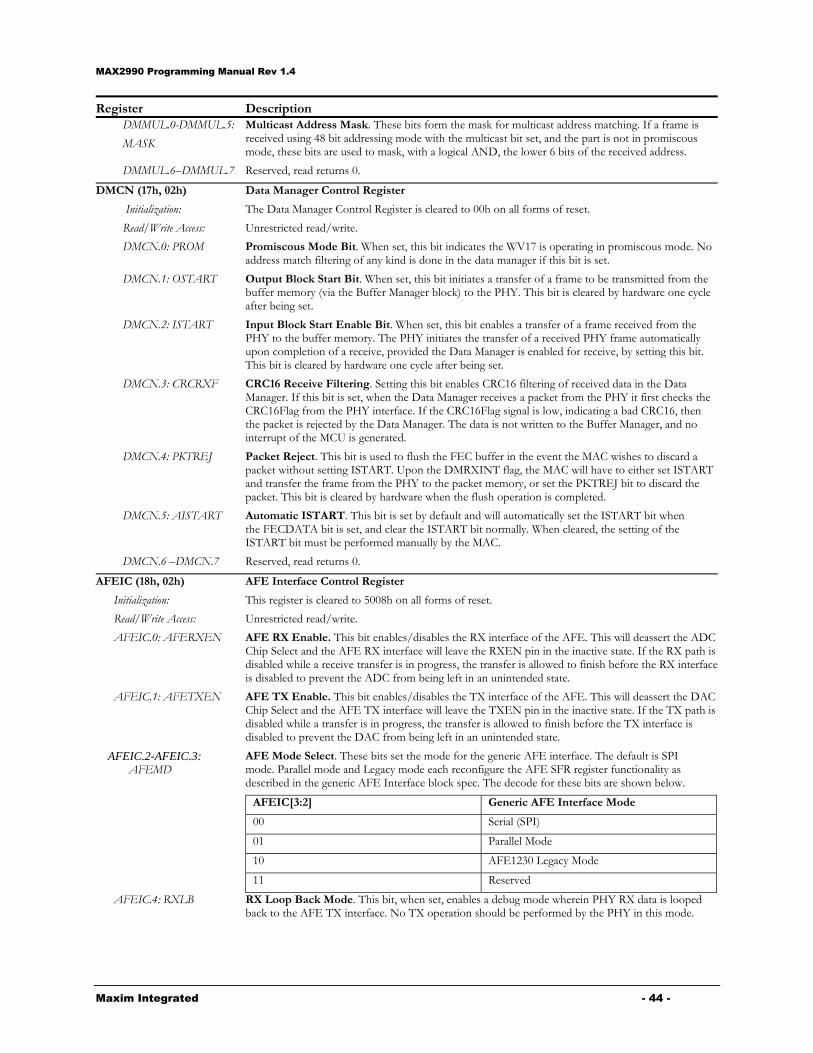
MAX2990 Programming Manual Rev 1.4
Maxim Integrated - 44 -
Register Description DMMUL.0-DMMUL.5:
MASK
Multicast Address Mask. These bits form the mask for multicast address matching. If a frame is received using 48 bit addressing mode with the multicast bit set, and the part is not in promiscous mode, these bits are used to mask, with a logical AND, the lower 6 bits of the received address.
DMMUL.6–DMMUL.7 Reserved, read returns 0.
DMCN (17h, 02h)
Initialization:
Read/Write Access:
Data Manager Control Register
The Data Manager Control Register is cleared to 00h on all forms of reset.
Unrestricted read/write.
DMCN.0: PROM Promiscous Mode Bit. When set, this bit indicates the WV17 is operating in promiscous mode. No address match filtering of any kind is done in the data manager if this bit is set.
DMCN.1: OSTART Output Block Start Bit. When set, this bit initiates a transfer of a frame to be transmitted from the buffer memory (via the Buffer Manager block) to the PHY. This bit is cleared by hardware one cycle after being set.
DMCN.2: ISTART Input Block Start Enable Bit. When set, this bit enables a transfer of a frame received from the PHY to the buffer memory. The PHY initiates the transfer of a received PHY frame automatically upon completion of a receive, provided the Data Manager is enabled for receive, by setting this bit. This bit is cleared by hardware one cycle after being set.
DMCN.3: CRCRXF CRC16 Receive Filtering. Setting this bit enables CRC16 filtering of received data in the Data Manager. If this bit is set, when the Data Manager receives a packet from the PHY it first checks the CRC16Flag from the PHY interface. If the CRC16Flag signal is low, indicating a bad CRC16, then the packet is rejected by the Data Manager. The data is not written to the Buffer Manager, and no interrupt of the MCU is generated.
DMCN.4: PKTREJ Packet Reject. This bit is used to flush the FEC buffer in the event the MAC wishes to discard a packet without setting ISTART. Upon the DMRXINT flag, the MAC will have to either set ISTART and transfer the frame from the PHY to the packet memory, or set the PKTREJ bit to discard the packet. This bit is cleared by hardware when the flush operation is completed.
DMCN.5: AISTART Automatic ISTART. This bit is set by default and will automatically set the ISTART bit when the FECDATA bit is set, and clear the ISTART bit normally. When cleared, the setting of the ISTART bit must be performed manually by the MAC.
DMCN.6 –DMCN.7 Reserved, read returns 0.
AFEIC (18h, 02h)
Initialization:
Read/Write Access:
AFE Interface Control Register
This register is cleared to 5008h on all forms of reset.
Unrestricted read/write.
AFEIC.0: AFERXEN AFE RX Enable. This bit enables/disables the RX interface of the AFE. This will deassert the ADC Chip Select and the AFE RX interface will leave the RXEN pin in the inactive state. If the RX path is disabled while a receive transfer is in progress, the transfer is allowed to finish before the RX interface is disabled to prevent the ADC from being left in an unintended state.
AFEIC.1: AFETXEN AFE TX Enable. This bit enables/disables the TX interface of the AFE. This will deassert the DAC Chip Select and the AFE TX interface will leave the TXEN pin in the inactive state. If the TX path is disabled while a transfer is in progress, the transfer is allowed to finish before the TX interface is disabled to prevent the DAC from being left in an unintended state.
AFEIC.2-AFEIC.3: AFEMD
AFE Mode Select. These bits set the mode for the generic AFE interface. The default is SPI mode. Parallel mode and Legacy mode each reconfigure the AFE SFR register functionality as described in the generic AFE Interface block spec. The decode for these bits are shown below.
AFEIC[3:2] Generic AFE Interface Mode
00 Serial (SPI)
01 Parallel Mode
10 AFE1230 Legacy Mode
11 Reserved
AFEIC.4: RXLB RX Loop Back Mode. This bit, when set, enables a debug mode wherein PHY RX data is looped back to the AFE TX interface. No TX operation should be performed by the PHY in this mode.

MAX2990 Programming Manual Rev 1.4
Maxim Integrated - 45 -
Register Description AFEIC.5: SWRT Single Write Configuration Mode. Setting this bit will transfer the contents of the AFETXC1
register, using the settings of the AFETXC0 register to allow the MCU to send a configuration frame to the serially connected device in SPI mode only. This bit is ignored in legacy or parallel modes. This allows configuration, sleep, wake-from-sleep, etc to be sent without activating the PHY TX path. This bit is cleared by hardware when the transfer of the configuration frame is complete.
AFEIC.6: RXENPL RX Enable Polarity. If this bit is '0', the AFE_RXEN pin is active low. If this bit is set to '1', then the AFE_RXEN pin is active high.
AFEIC.7: TXENPL TX Enable Polarity. If this bit is '0', the AFE_TXEN pin is active low. If this bit is set to '1', then the AFE_TXEN pin is active high.
AFEIC.8: RXCLKINV RX CLK Invert. If this bit is set to '1', the AFE_RXCLK pin is inverted, to capture data from the ADC on the negative edge of the receive clock. If this bit is '0', then the AFE_RXCLK pin is sent out uninverted and data is received relative to the positive edge of the receive clock.
AFEIC9: TXCLKINV TX CLK Invert. If this bit is set to '1', the AFE_TXCLK pin is inverted so that data sent to the DAC is clocked on the negative edge of the transmit clock. If this bit is '0', then the AFE_TXCLK pin is sent out uninverted and data is sent relative to the positive edge of the transmit clock.
AFEIC10: ADCFMT ADC Format. If this bit is set to '0', the data received on the AFE_SDI pin is in twos complement binary. If this bit is '1', the received data is in unsigned binary.
AFEIC11: DACFMT DAC Format. If this bit is set to '0', the data sent on the AFE_SDO pin is in twos complement binary. If this bit is '1', the sent data is in unsigned binary.
AFEIC.12-AFEIC.13:
RXGAIN
RX Gain. The bits set the RX gain factor as shown:
AFEIC[13:12] RX Gain
00 Divide by 2
01 Divide by 1
10 Multiply by 2
11 Multiply by 4
AFEIC.15-AFEIC.14:
TXGAIN
TX Gain. The bits set the TX gain factor as shown:
AFEIC[15:14] TX Gain
00 Multiply by 2
01 Divide by 1
10 Divide by 2
11 Divide by 4
AFERXC (19h, 02h)
Initialization:
Read/Write Access:
AFE RX Control Register
This register is cleared to 0040h on all forms of reset.
Unrestricted read/write, except ADCRES which is read only.
AFERXC.0–AFERXC.1:
ADCDL
ADC Data Length. These bits define the data length, as 8, 10, 12 or 14, bits for the RX AFE SPI frame. 2'b00 indicates an 8 bit data word is embedded in the 16 bit data frame from the external ADC. A 2'b01 = 10 bits, 2'b10 = 12 bits and 2'b11 indicates a 14 bit word.
AFERXC.2 Reserved, read returns zero.
AFERXC.3–AFERXC.5:
ADCDP
ADC Data Position. These bits define the position of the LSB of the received data word from the ADC within the 16 bit RX SPI frame. A 3'b000 indicates the LSB of the data word received from the AFE RX interface will start with the very first bit received within the 16 bit SPI frame. A value of 3'b001 indicates there is one non-data bit received prior to the data word and so on. Together with the ADCDL bits this allows the AFE to pick off the data word from the ADC within the SPI receive frame.
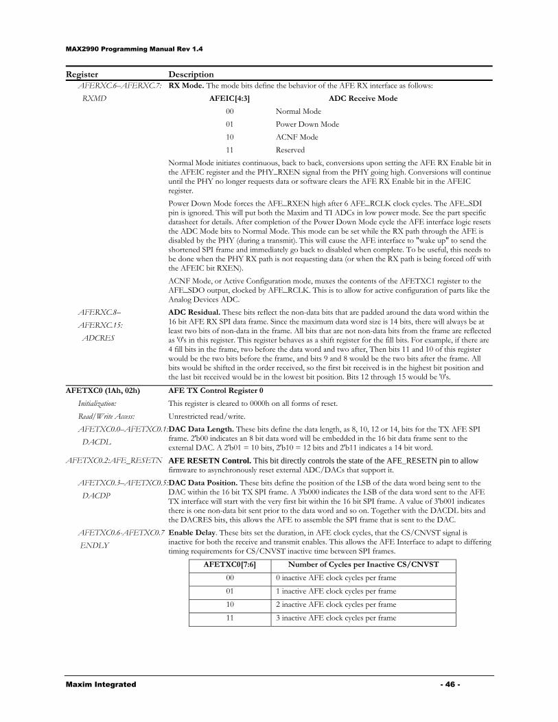
MAX2990 Programming Manual Rev 1.4
Maxim Integrated - 46 -
Register Description AFERXC.6–AFERXC.7:
RXMD
RX Mode. The mode bits define the behavior of the AFE RX interface as follows:
AFEIC[4:3] ADC Receive Mode
00 Normal Mode
01 Power Down Mode
10 ACNF Mode
11 Reserved
Normal Mode initiates continuous, back to back, conversions upon setting the AFE RX Enable bit in the AFEIC register and the PHY_RXEN signal from the PHY going high. Conversions will continue until the PHY no longer requests data or software clears the AFE RX Enable bit in the AFEIC register.
Power Down Mode forces the AFE_RXEN high after 6 AFE_RCLK clock cycles. The AFE_SDI pin is ignored. This will put both the Maxim and TI ADCs in low power mode. See the part specific datasheet for details. After completion of the Power Down Mode cycle the AFE interface logic resets the ADC Mode bits to Normal Mode. This mode can be set while the RX path through the AFE is disabled by the PHY (during a transmit). This will cause the AFE interface to "wake up" to send the shortened SPI frame and immediately go back to disabled when complete. To be useful, this needs to be done when the PHY RX path is not requesting data (or when the RX path is being forced off with the AFEIC bit RXEN).
ACNF Mode, or Active Configuration mode, muxes the contents of the AFETXC1 register to the AFE_SDO output, clocked by AFE_RCLK. This is to allow for active configuration of parts like the Analog Devices ADC.
AFERXC.8–
AFERXC.15:
ADCRES
ADC Residual. These bits reflect the non-data bits that are padded around the data word within the 16 bit AFE RX SPI data frame. Since the maximum data word size is 14 bits, there will always be at least two bits of non-data in the frame. All bits that are not non-data bits from the frame are reflected as '0's in this register. This register behaves as a shift register for the fill bits. For example, if there are 4 fill bits in the frame, two before the data word and two after, Then bits 11 and 10 of this register would be the two bits before the frame, and bits 9 and 8 would be the two bits after the frame. All bits would be shifted in the order received, so the first bit received is in the highest bit position and the last bit received would be in the lowest bit position. Bits 12 through 15 would be '0's.
AFETXC0 (1Ah, 02h)
Initialization:
Read/Write Access:
AFE TX Control Register 0
This register is cleared to 0000h on all forms of reset.
Unrestricted read/write.
AFETXC0.0–AFETXC0.1:
DACDL
DAC Data Length. These bits define the data length, as 8, 10, 12 or 14, bits for the TX AFE SPI frame. 2'b00 indicates an 8 bit data word will be embedded in the 16 bit data frame sent to the external DAC. A 2'b01 = 10 bits, 2'b10 = 12 bits and 2'b11 indicates a 14 bit word.
AFETXC0.2:AFE_RESETN AFE RESETN Control. This bit directly controls the state of the AFE_RESETN pin to allow firmware to asynchronously reset external ADC/DACs that support it.
AFETXC0.3–AFETXC0.5:
DACDP
DAC Data Position. These bits define the position of the LSB of the data word being sent to the DAC within the 16 bit TX SPI frame. A 3'b000 indicates the LSB of the data word sent to the AFE TX interface will start with the very first bit within the 16 bit SPI frame. A value of 3'b001 indicates there is one non-data bit sent prior to the data word and so on. Together with the DACDL bits and the DACRES bits, this allows the AFE to assemble the SPI frame that is sent to the DAC.
AFETXC0.6-AFETXC0.7
ENDLY
Enable Delay. These bits set the duration, in AFE clock cycles, that the CS/CNVST signal is inactive for both the receive and transmit enables. This allows the AFE Interface to adapt to differing timing requirements for CS/CNVST inactive time between SPI frames.
AFETXC0[7:6] Number of Cycles per Inactive CS/CNVST
00 0 inactive AFE clock cycles per frame
01 1 inactive AFE clock cycles per frame
10 2 inactive AFE clock cycles per frame
11 3 inactive AFE clock cycles per frame
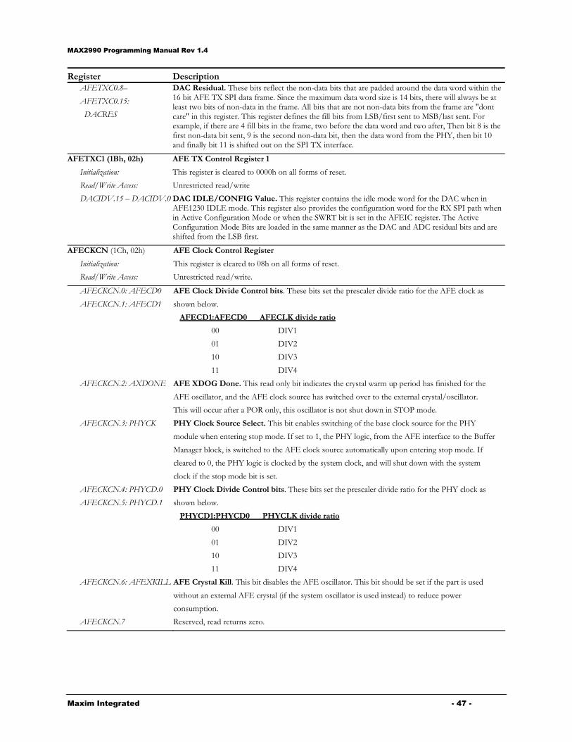
MAX2990 Programming Manual Rev 1.4
Maxim Integrated - 47 -
Register Description AFETXC0.8–
AFETXC0.15:
DACRES
DAC Residual. These bits reflect the non-data bits that are padded around the data word within the 16 bit AFE TX SPI data frame. Since the maximum data word size is 14 bits, there will always be at least two bits of non-data in the frame. All bits that are not non-data bits from the frame are "dont care" in this register. This register defines the fill bits from LSB/first sent to MSB/last sent. For example, if there are 4 fill bits in the frame, two before the data word and two after, Then bit 8 is the first non-data bit sent, 9 is the second non-data bit, then the data word from the PHY, then bit 10 and finally bit 11 is shifted out on the SPI TX interface.
AFETXC1 (1Bh, 02h)
Initialization:
Read/Write Access:
DACIDV.15 – DACIDV.0
AFE TX Control Register 1
This register is cleared to 0000h on all forms of reset.
Unrestricted read/write
DAC IDLE/CONFIG Value. This register contains the idle mode word for the DAC when in AFE1230 IDLE mode. This register also provides the configuration word for the RX SPI path when in Active Configuration Mode or when the SWRT bit is set in the AFEIC register. The Active Configuration Mode Bits are loaded in the same manner as the DAC and ADC residual bits and are shifted from the LSB first.
AFECKCN (1Ch, 02h)
Initialization:
Read/Write Access:
AFE Clock Control Register
This register is cleared to 08h on all forms of reset.
Unrestricted read/write.
AFECKCN.0: AFECD0
AFECKCN.1: AFECD1
AFECKCN.2: AXDONE
AFECKCN.3: PHYCK
AFECKCN.4: PHYCD.0
AFECKCN.5: PHYCD.1
AFECKCN.6: AFEXKILL
AFECKCN.7
AFE Clock Divide Control bits. These bits set the prescaler divide ratio for the AFE clock as
shown below.
AFECD1:AFECD0 AFECLK divide ratio
00 DIV1
01 DIV2
10 DIV3
11 DIV4
AFE XDOG Done. This read only bit indicates the crystal warm up period has finished for the
AFE oscillator, and the AFE clock source has switched over to the external crystal/oscillator.
This will occur after a POR only, this oscillator is not shut down in STOP mode.
PHY Clock Source Select. This bit enables switching of the base clock source for the PHY
module when entering stop mode. If set to 1, the PHY logic, from the AFE interface to the Buffer
Manager block, is switched to the AFE clock source automatically upon entering stop mode. If
cleared to 0, the PHY logic is clocked by the system clock, and will shut down with the system
clock if the stop mode bit is set.
PHY Clock Divide Control bits. These bits set the prescaler divide ratio for the PHY clock as
shown below.
PHYCD1:PHYCD0 PHYCLK divide ratio
00 DIV1
01 DIV2
10 DIV3
11 DIV4
AFE Crystal Kill. This bit disables the AFE oscillator. This bit should be set if the part is used
without an external AFE crystal (if the system oscillator is used instead) to reduce power
consumption.
Reserved, read returns zero.

MAX2990 Programming Manual Rev 1.4
Maxim Integrated - 48 -
Register Description TB0R (00h, 03h)
Initialization:
Read/Write Access:
Timer 0 Capture/Reload Value
This register is cleared to x0000h on all forms of reset.
Unrestricted Read/Write
TB0R.15 – TB0R.0 Timer 0 Capture/Reload Bits 15:0. This register is used to capture the TBV value when Timer B is configured in capture mode. This register is also used as the 16-bit reload value when Timer B is configured in auto-reload mode.
TB0C (01h, 03h)
Initialization:
Read/Write Access:
Timer 0 Compare
This register is cleared to 0000h on all forms of reset.
Unrestricted Read/Write
TB0C.15 – TB0C.0 Timer 0 Compare Bits 15:0. This register is used for comparison versus the TBV value when Timer B is operated in compare mode.
TB1R (02h, 03h) Timer 1 Capture/Reload Value (see TB0R register bit descriptions)
TB1C (03h, 03h) Timer 1 Compare (see TB0C register bit descriptions)
TB2R (04h, 03h) Timer 2 Capture/Reload Value (see TB0R register bit descriptions)
TB2C (05h, 03h) Timer 2 Compare (see TB0C register bit descriptions)
TB3R (06h, 03h) Timer 3 Capture/Reload Value (see TB0R register bit descriptions)
TB3C (07h, 03h) Timer 3 Compare (see TB0C register bit descriptions)
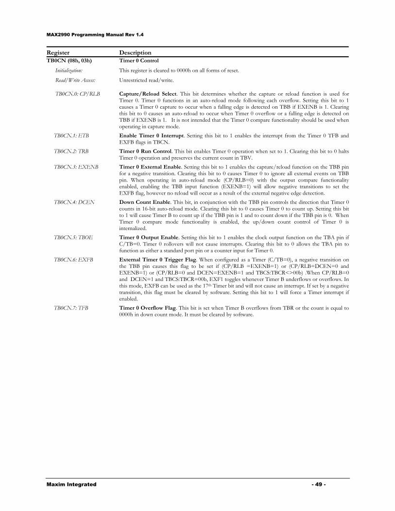
MAX2990 Programming Manual Rev 1.4
Maxim Integrated - 49 -
Register Description TB0CN (08h, 03h)
Initialization:
Read/Write Access:
Timer 0 Control
This register is cleared to 0000h on all forms of reset.
Unrestricted read/write.
TB0CN.0: CP/RLB
Capture/Reload Select. This bit determines whether the capture or reload function is used forTimer 0. Timer 0 functions in an auto-reload mode following each overflow. Setting this bit to 1 causes a Timer 0 capture to occur when a falling edge is detected on TBB if EXENB is 1. Clearing this bit to 0 causes an auto-reload to occur when Timer 0 overflow or a falling edge is detected onTBB if EXENB is 1. It is not intended that the Timer 0 compare functionality should be used whenoperating in capture mode.
TB0CN.1: ETB Enable Timer 0 Interrupt. Setting this bit to 1 enables the interrupt from the Timer 0 TFB andEXFB flags in TBCN.
TB0CN.2: TRB Timer 0 Run Control. This bit enables Timer 0 operation when set to 1. Clearing this bit to 0 haltsTimer 0 operation and preserves the current count in TBV.
TB0CN.3: EXENB
Timer 0 External Enable. Setting this bit to 1 enables the capture/reload function on the TBB pinfor a negative transition. Clearing this bit to 0 causes Timer 0 to ignore all external events on TBB pin. When operating in auto-reload mode (CP/RLB=0) with the output compare functionality enabled, enabling the TBB input function (EXENB=1) will allow negative transitions to set theEXFB flag, however no reload will occur as a result of the external negative edge detection.
TB0CN.4: DCEN
Down Count Enable. This bit, in conjunction with the TBB pin controls the direction that Timer 0counts in 16-bit auto-reload mode. Clearing this bit to 0 causes Timer 0 to count up. Setting this bit to 1 will cause Timer B to count up if the TBB pin is 1 and to count down if the TBB pin is 0. WhenTimer 0 compare mode functionality is enabled, the up/down count control of Timer 0 isinternalized.
TB0CN.5: TBOE
Timer 0 Output Enable. Setting this bit to 1 enables the clock output function on the TBA pin ifC/TB=0. Timer 0 rollovers will not cause interrupts. Clearing this bit to 0 allows the TBA pin tofunction as either a standard port pin or a counter input for Timer 0.
TB0CN.6: EXFB
External Timer 0 Trigger Flag. When configured as a Timer (C/TB=0), a negative transition on the TBB pin causes this flag to be set if (CP/RLB =EXENB=1) or (CP/RLB=DCEN=0 andEXENB=1) or (CP/RLB=0 and DCEN=EXENB=1 and TBCS:TBCR<>00b) .When CP/RLB=0and DCEN=1 and TBCS:TBCR=00b, EXF1 toggles whenever Timer B underflows or overflows. Inthis mode, EXFB can be used as the 17th Timer bit and will not cause an interrupt. If set by a negative transition, this flag must be cleared by software. Setting this bit to 1 will force a Timer interrupt if enabled.
TB0CN.7: TFB Timer 0 Overflow Flag. This bit is set when Timer B overflows from TBR or the count is equal to0000h in down count mode. It must be cleared by software.

MAX2990 Programming Manual Rev 1.4
Maxim Integrated - 50 -
Register Description TB0CN.10-8: TBPS2:0
Timer 0 Clock Prescaler Bits 2:0. The TBPS2:0 bits select the clock prescaler applied to the system clock input to Timer 0.
Timer 0 Clock = System Clock/2(2xTBPS2:0)
TBPS2:0 Timer B Input Clock
000 Sysclk/1
001 Sysclk/4
010 Sysclk/16
011 Sysclk/64
100 Sysclk/256
101 Sysclk/1024
11x Reserved
TB0CN.11.TBCR
TB0CN.12:TBCS
Timer 0 Compare Mode Reset.
Timer 0 Compare Mode Set.
These compare mode bits define whether the PWM/Compare Mode output function is enabled onthe TBB pin, the initial output starting state, and what compare mode output function is in effect.When the timer is not running (TRB=0), the initial output starting state of the TBB output isestablished as low or high respectively if the Reset function (TBCR=1,TBCS=0) or Set function (TBCR=0, TBCS=1) is established. Invoking the toggle function does not change the already definedstarting state for TBB. The initial starting state will take effect on the pin when the Timer is started(TRB=1). Changing the output function to Set or Reset while the Timer is running does affect the current output. The table below summarizes the compare output function when the compare (TBC)register is present and when it is not.
TBCS:TBCR Function
(TBC register exists)
Function
(no TBC register)
Initial State (if
TRB=0)
00 None (Compare Disable) None (Compare Disable) No change
01 Reset on TBC Match, Set on 0000h Set on 0000h Low
10 Set on TBC Match, Reset on TBR Match Reset on TBR Match High
11 Toggle on TBC Match (except TBR or 0h) Toggle on TBR Match No change
TB0CN.14-13 Reserved, read returns 0. These bits are reserved for future addition of TBCRn, TBCSn Output
compare bits for a second compare strobe that operates from the same Timer 0.
TB0CN.15: C/TB Counter/Timer Select. This bit determines whether Timer B functions as a Timer or counter.Setting this bit to 1 causes Timer 0 to count negative transitions on the TBA pin. Clearing this bit to 0causes Timer 0 to function as a Timer. The speed of Timer B is determined by the TBPS2:0 bits of TBCN.
TB0V (09h, 03h)
Initialization:
Read/Write Access:
Timer 0 Value Register
The Timer B Value is cleared to x0000h on all forms of reset.
Unrestricted Read/Write
TB0V.15 – TB0V.0 Timer 0 Value Bits 15:0. This register is used to load and read the 16-bit Timer 0 value.
TB1CN (0Ah, 03h) Timer 1 Control Register (see TB0CN register bit descriptions)
TB1V (0Bh, 03h) Timer 1 Value Register (see TB0V register bit descriptions)
TB2CN (0Ch, 03h) Timer 2 Control Register (see TB0CN register bit descriptions.)
TB2V (0Dh, 03h) Timer 2 Value Register (see TB0V register bit descriptions)
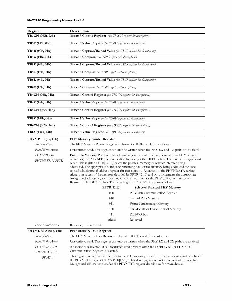
MAX2990 Programming Manual Rev 1.4
Maxim Integrated - 51 -
Register Description TB3CN (0Eh, 03h) Timer 3 Control Register (see TB0CN register bit descriptions)
TB3V (0Fh, 03h) Timer 3 Value Register (see TB0V register bit descriptions)
TB4R (00h, 04h) Timer 4 Capture/Reload Value (see TB0R register bit descriptions)
TB4C (01h, 04h) Timer 4 Compare (see TB0C register bit descriptions)
TB5R (02h, 04h) Timer 5 Capture/Reload Value (see TB0R register bit descriptions)
TB5C (03h, 04h) Timer 5 Compare (see TB0C register bit descriptions)
TB6R (04h, 04h) Timer 6 Capture/Reload Value (see TB0R register bit descriptions)
TB6C (05h, 04h) Timer 6 Compare (see TB0C register bit descriptions)
TB4CN (08h, 04h) Timer 4 Control Register (see TB0CN register bit descriptions.)
TB4V (09h, 04h) Timer 4 Value Register (see TB0V register bit descriptions)
TB5CN (0Ah, 04h) Timer 5 Control Register (see TB0CN register bit descriptions.)
TB5V (0Bh, 04h) Timer 5 Value Register (see TB0V register bit descriptions)
TB6CN (0Ch, 04h) Timer 6 Control Register (see TB0CN register bit descriptions.)
TB6V (0Dh, 04h) Timer 6 Value Register (see TB0V register bit descriptions)
PHYMPTR (0h, 05h)
Initialization:
Read/Write Access:
PHY Memory Pointer Register
The PHY Memory Pointer Register is cleared to 0000h on all forms of reset.
Unrestricted read. This register can only be written when the PHY RX and TX paths are disabled.
PHYMPTR.0-
PHYMPTR.12:PPTR
Preamble Memory Pointer. This address register is used to write to one of three PHY physical memories, the PHY SFR Communication Register, or the DEBUG bus. The three most significant bits of this register ,PPTR[12:10], select the physical memory or register interface being addressed. The appropriate number of remaining bits for the memory being addressed are used to load a background address register for that memory. An access to the PHYMDATA register triggers an access of the memory decoded by PPTR[12:10] and post-increments the appropriate background address register. Post increment is not done for the PHY SFR Communication Register or the DEBUG bus. The decoding for PPTR[12:10] is shown below:
PPTR[12:10] Selected Physical PHY Memory
000 PHY SFR Communication Register
010 Symbol Data Memory
011 Frame Synchronizer Memory
100 TX Modulator Phase Control Memory
111 DEBUG Bus
others Reserved
PMA.13–PMA.15 Reserved, read returns 0.
PHYMDATA (01h, 05h)
Initialization:
Read/Write Access:
PHYMDATA.0-
PHYMDATA.15:
PDATA
PHY Memory Data Register
The PHY Memory Data Register is cleared to 0000h on all forms of reset.
Unrestricted read. This register can only be written when the PHY RX and TX paths are disabled.
if a memory is selected. It is unrestricted read or write when the DEBUG bus or PHY SFR Communication Register is selected.
This register initiates a write of data to the PHY memory selected by the two most significant bits of the PHYMPTR register (PHYMPTR[12:0]). This also triggers the post increment of the selected background address register. See the PHYMPTR register description for more details.

MAX2990 Programming Manual Rev 1.4
Maxim Integrated - 52 -
Register Description PCTHR (02h, 05h)
Initialization:
Read/Write Access:
PCTHR.0-PCTHR.15:
CHANNEL_THR
Channel Threshold Register
The Channel Threshold Register is cleared to 0000h on all forms of reset.
Unrestricted read/write.
This register sets the threshold for doing channel estimation.
PCR (03h, 05h)
Initialization:
Read/Write Access:
PHY Control Register
The PHY Control Register is cleared to 0000h on all forms of reset.
Unrestricted read/write.
PCR.0: TXRetran
Start Retransmit. When set, this bit initiate a re-transmit of the frame of data already stored in the PHY buffer, in the event a NAK is received upon completion of a tranmit operation. Data should have already been transferred from the buffer memory to the PHY, so this bit must be set prior to a new frame being transferred from the buffer memory. This bit is cleared by hardware one cycle after being set.
PCR.1: ACKstart Start ACK. Setting this bit starts the transmission of an ACK packet. This bit is cleared by hardware one cycle after being set.
PCR.2: PHYEN PHY Enable. When set, this bit enables the clock to the PHY. When cleared, the clock to the PHY transmit path will be gated off.
PCR.3: PHYMOD PHY Mode. This bit selects either transmit or receive mode for the PHY. When set, this bit enables the PHY transmit path and disables the receive path. When cleared, the PHY receive path is enabled and the transmit path is disabled.
PCR.4: JDEN Jammer Detector Enable. Setting this bit enables the Jammer Detection circuitry.
PCR.5: JCEN Jammer Canceller Enable. Setting this bit enables the Jammer Canceller circuitry.
PCR.6: HPFEN DC Blocker Enable. Setting this bit enables the DC Blocker circuitry.
PCR.7: TXROBOEN TXROBO Mode Enable. If set, this bit enables Robust mode (ROBO) for the PHY transmit path. If zero, the PHY transmitter will operate in normal mode.
PCR.8: DAGCEN Digital Automatic Gain Control Enable. Setting this bit enables the Digital Automatic Gain Control circuitry.
PCR.9: DAGCFRZ Digital Automatic Gain Control Freeze. Setting this bit disables the automatic adjustment of gain in the Digital Automatic Gain Control circuitry and uses a fixed gain/attenuation factor instead, essentially overriding the AGC with a manual setting. The AAFO bit in the AGC4 register controls whether the AGC is locked into attenuating or amplifying and the gain shift value (GS) in the AGC4 register sets the attenuation/gain value.
PCR.10-PCR.11:
RXMD
Receive Mode. These bits set the receive mode of the demodulator as shown below:
RXMD[1:0] RX Mode
00 Auto Mode
01 Normal Mode
10 ROBO Mode
11 Invalid
PCR.12: RXRST RX Reset. Setting this bit resets the receive path in the PHY. This bit is OR'd with the global RSTN. When set by software, this bit will be cleared by hardware when the reset is complete.
PCR.13: TXRST TX Reset. Setting this bit resets the transmit path in the PHY. This bit is OR'd with the global RSTN. When set by software, this bit will be cleared by hardware when the reset is complete.
PCR.14: CRCEN CRC16 Enable. This bit enables or disables the CRC16 calculations for PHY frames. If set to '1', a CRC16 checksum is calculated for each outgoing PHY frame and appended to the data. If cleared to '0', the transmitter does not append a CRC16 checksum to the frame, and only data is sent. On the receive side, a CRC16 checksum is always calculated for all received data and compared to the received CRC16 checksum (last two bytes). This is done regardless of the state of the CRCEN bit. If the transmitter did not calculate and append a CRC16 checksum, the receiver will simply have a CRC16 failure (reflected in the CRCOK bit in the PSR register) and software will ignore the CRC result.
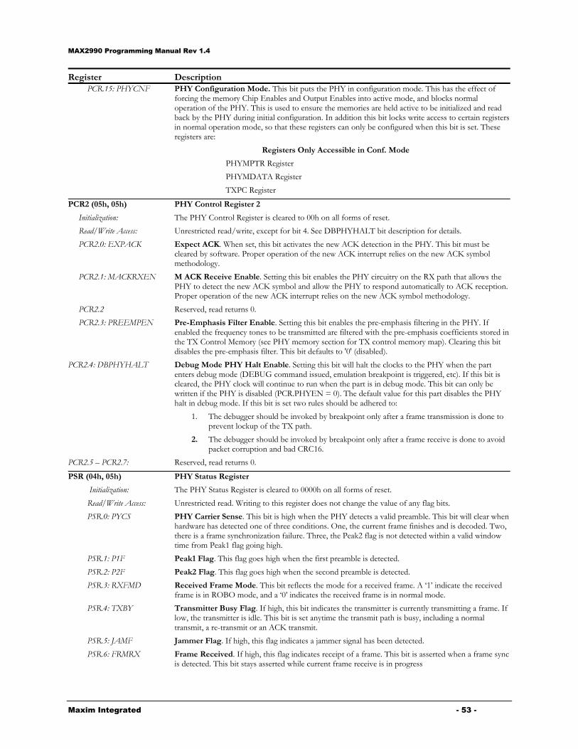
MAX2990 Programming Manual Rev 1.4
Maxim Integrated - 53 -
Register Description PCR.15: PHYCNF PHY Configuration Mode. This bit puts the PHY in configuration mode. This has the effect of
forcing the memory Chip Enables and Output Enables into active mode, and blocks normal operation of the PHY. This is used to ensure the memories are held active to be initialized and read back by the PHY during initial configuration. In addition this bit locks write access to certain registers in normal operation mode, so that these registers can only be configured when this bit is set. These registers are:
Registers Only Accessible in Conf. Mode
PHYMPTR Register
PHYMDATA Register
TXPC Register
PCR2 (05h, 05h)
Initialization:
Read/Write Access:
PHY Control Register 2
The PHY Control Register is cleared to 00h on all forms of reset.
Unrestricted read/write, except for bit 4. See DBPHYHALT bit description for details.
PCR2.0: EXPACK Expect ACK. When set, this bit activates the new ACK detection in the PHY. This bit must be cleared by software. Proper operation of the new ACK interrupt relies on the new ACK symbol methodology.
PCR2.1: MACKRXEN M ACK Receive Enable. Setting this bit enables the PHY circuitry on the RX path that allows the PHY to detect the new ACK symbol and allow the PHY to respond automatically to ACK reception. Proper operation of the new ACK interrupt relies on the new ACK symbol methodology.
PCR2.2 Reserved, read returns 0.
PCR2.3: PREEMPEN Pre-Emphasis Filter Enable. Setting this bit enables the pre-emphasis filtering in the PHY. If enabled the frequency tones to be transmitted are filtered with the pre-emphasis coefficients stored in the TX Control Memory (see PHY memory section for TX control memory map). Clearing this bit disables the pre-emphasis filter. This bit defaults to '0' (disabled).
PCR2.4: DBPHYHALT Debug Mode PHY Halt Enable. Setting this bit will halt the clocks to the PHY when the part enters debug mode (DEBUG command issued, emulation breakpoint is triggered, etc). If this bit is cleared, the PHY clock will continue to run when the part is in debug mode. This bit can only be written if the PHY is disabled (PCR.PHYEN = 0). The default value for this part disables the PHY halt in debug mode. If this bit is set two rules should be adhered to:
1. The debugger should be invoked by breakpoint only after a frame transmission is done to prevent lockup of the TX path.
2. The debugger should be invoked by breakpoint only after a frame receive is done to avoid packet corruption and bad CRC16.
PCR2.5 – PCR2.7: Reserved, read returns 0.
PSR (04h, 05h)
Initialization:
Read/Write Access:
PHY Status Register
The PHY Status Register is cleared to 0000h on all forms of reset.
Unrestricted read. Writing to this register does not change the value of any flag bits.
PSR.0: PYCS
PHY Carrier Sense. This bit is high when the PHY detects a valid preamble. This bit will clear when hardware has detected one of three conditions. One, the current frame finishes and is decoded. Two, there is a frame synchronization failure. Three, the Peak2 flag is not detected within a valid window time from Peak1 flag going high.
PSR.1: P1F Peak1 Flag. This flag goes high when the first preamble is detected.
PSR.2: P2F Peak2 Flag. This flag goes high when the second preamble is detected.
PSR.3: RXFMD Received Frame Mode. This bit reflects the mode for a received frame. A ‘1’ indicate the received frame is in ROBO mode, and a ‘0’ indicates the received frame is in normal mode.
PSR.4: TXBY Transmitter Busy Flag. If high, this bit indicates the transmitter is currently transmitting a frame. If low, the transmitter is idle. This bit is set anytime the transmit path is busy, including a normal transmit, a re-transmit or an ACK transmit.
PSR.5: JAMF Jammer Flag. If high, this flag indicates a jammer signal has been detected.
PSR.6: FRMRX Frame Received. If high, this flag indicates receipt of a frame. This bit is asserted when a frame sync is detected. This bit stays asserted while current frame receive is in progress
MAX2990 Programming Manual Rev 1.4
Maxim Integrated - 54 -
Register Description PSR.7: CRCOK CRC OK. If high, this flag indicates the received frame CRC16 checksum is valid. A low value
indicates the CRC16 checksum is invalid.
PSR.8: ATEN Attenuation Flag. If high, this flag indicates the AGC is attenuating data. If clear, the AGC is amplifying data. This flag is only valid if the AGC is enabled, if the AGC is not enabled this flag will always return 0.
PSR.9: FECDATA FEC Data. This bit indicates there is data in the FEC buffer. It is used by the MAC software to determine if there is a frame in the RXFEC waiting to be read or flushed by the data manager. This bit is needed to help MAC assess the state of RXFEC if it fails to set ISTART bit on time after an RX interrupt and causing the PHY to stay in a waiting state. If another frame arrives during this period it will create a lock up condition in the logic. A PHY RX reset is required if the lock up situation does occur.
PSR.15-PSR.10 Reserved, returns 0.
AGC1 (07h, 05h)
Initialization:
Read/Write Access:
AFF.0:AFF.15
AGC Control Register 1 - AGC Forget Factor
The AGC Control Register 1 is cleared to 007Ch on all forms of reset.
Unrestricted read/write.
This register contains the forget factor for the Automatic Gain Control Circuitry. The forget factor specifies the effective length of the window we are computing energy on.
AGC2 (08h, 05h)
Initialization:
Read/Write Access:
ADE.0:ADE.15
AGC Control Register 2 - AGC Desired Energy
The AGC Control Register 2 is cleared to 00F0h on all forms of reset.
Unrestricted read/write.
This register contains the desired energy level for the output of the Automatic Gain Control Circuitry.
AGC3 (09h, 05h)
Initialization:
Read/Write Access:
AWL.0:AWL.15
AGC Control Register 3 - AGC Window Length
The AGC Control Register 3 is cleared to 00FFh on all forms of reset.
Unrestricted read/write.
This register contains the window length for the Automatic Gain Control Circuitry. The window length specifies the interval after which we can update the AGC gain.
AGC4 (0Ah, 05h)
Initialization:
Read/Write Access:
AGC Control Register 4 - AGC Gain Shift and Window Shift
The AGC Control Register 4 is cleared to 0008h on all forms of reset.
Unrestricted read/write.
AGC4.0-AGC4.3:
AWS
AGC Window Shift. These bits set the programmable window shift for the Automatic Gain Control Circuitry.
AGC4.4-AGC4.7:
AGS
AGC Gain Shift. These bits set the programmable gain shift for the Automatic Gain Control Circuitry.
AGC4.8: AAFO AGC Attenuation Flag Override. This bit determines whether the AGC circuitry is attenuating or amplifying if the DAGCFRZ bit is set. If the DAGCFRZ bit is not set this bit has no meaning. If the AAFO bit is set to '1' the AGC will be forced to attenuate. If it is cleared to '0' the AGC will be forced to amplify.
AGC4.9: RMSMD RMS Mode. This bit controls the mode of the RMS block. When set (‘1’) the RMS block is in “free running” mode and will make energy calculations after a fixed time that will include noise. If the bit is cleared (‘0’) the RMS block is not in free running mode and will start energy calculations on the start of data.
AGC4.10-AGC4.15 Reserved. Read returns zero
MAX2990 Programming Manual Rev 1.4
Maxim Integrated - 55 -
Register Description DEM (0Bh, 05h)
Initialization:
Read/Write Access:
Demodulator Control Register
The Demodulator Control Register is cleared to 001Ch on all forms of reset.
Unrestricted read/write.
DEM.0-DEM.7:
SYMOF
Symbol Offset. These bits set the symbol offset.
DEM.8-DEM.11:
SOFT
Soft Shift. These bits set the number of soft shifts.
DEM.12-DEM.15 Reserved. Read returns zero.
SYNC1 (0Ch, 05h)
Initialization:
Read/Write Access:
Synchronizer Control Register 1
The Synchronizer Control Register 1 is cleared to 020Ch on all forms of reset.
Unrestricted read/write.
SYNC1.0: SYNCMD
Synchronizer Mode. This bit sets the frame and symbol synchronizer modes. If set to ‘1’, the synchronizer is in wideband mode. If ‘0’, the synchronizer is in narrowband mode.
SYNC1.1-SYNC1.5:
NBSBS
Narrow Band Synchronizer Buffer Shift Register. These bits set the synchronizer shift value. It is always a positive (right) shift. Note that setting the NBSS bits to a value larger than 16h will result in clearing the filter output.
SYNC1.8-SYNC1.15:
SOFS
Synchronizer Offset. These bits set the synchronizer offset
SYNC1.6-SYNC1.7 Reserved, read returns 0.
SYNC2 (0Dh, 05h)
Initialization:
Read/Write Access:
Synchronizer Control Register 2
The Synchronizer Control Register 2 is cleared to 2A2Ah on all forms of reset.
Unrestricted read/write.
SYNC2.0-SYNC2.7:
P2TW
Peak2 Time Window. Sets the valid time window for Peak2 detection in the synchronizer.
SYNC2.8-SYNC2.15:
P1TW
Peak1 Time Window. Sets the valid time window for Peak1 detection in the synchronizer.
SYNC3 (0Eh, 05h)
Initialization:
Read/Write Access:
SYNC3.0-SYNC3.15:
P1THR
Synchronizer Control Register 3
The Synchronizer Control Register 3 is cleared to 02BCh on all forms of reset.
Unrestricted read/write.
Peak 1 Symbol Synchronizer Threshold 1. This register sets the symbol synchronizer threshold for Peak 1 detection.
SYNC4 (0Fh, 05h)
Initialization:
Read/Write Access:
SYNC4.0-SYNC4.15:
P2THR
Synchronizer Control Register 4
The Synchronizer Control Register 4 is cleared to 02BCh on all forms of reset.
Unrestricted read/write.
Peak 2 Symbol Synchronizer Threshold. This register sets the symbol synchronizer threshold for Peak 2 detection.
INTRL (10h, 05h)
Initialization:
Read/Write Access:
Interleaver/Deinterleaver Control Register
The Interleaver/Deinterleaver Control Register is cleared to 7464h on all forms of reset.
Unrestricted read/write.
INTRL.0-INTRL.6:
NCOL
Number of Interleaver Columns. This sets the number of columns in the interleaver/deinterleaver block.
INTRL.7-INTRL.15:
IOFS
Interleaver Offset. This sets the offset for the interleaver/deinterleaver block.
MAX2990 Programming Manual Rev 1.4
Maxim Integrated - 56 -
Register Description FEC1 (11h, 05h)
Initialization:
Read/Write Access:
FEC Control Register 1
The FEC Control Register 1 is cleared to 0084h on all forms of reset.
Unrestricted read/write.
FEC1.0-FEC1.4:
NMPAD
Number of Normal M Pads. This sets the number of ‘M’ padding bits in normal mode.
FEC1.5-FEC1.9:
RMPAD
Number of ROBO M Pads. This sets the number of ‘M’ padding bits in ROBO mode.
FEC1.10:RSPAR Reed-Solomon Parity Bytes. This bit sets the number of Reed-Solomon parity bytes. If set to 1, there will be 16 parity bytes. If cleared to 0, there will be 8 parity bytes.
FEC1.11–FEC1.15 Reserved, read returns 0.
FEC2 (12h, 05h)
Initialization:
Read/Write Access:
FEC Control Register 2
The FEC Control Register 2 is cleared to 3DF9h on all forms of reset.
Unrestricted read/write.
FEC2.0-FEC2.7:
RSNSZ
Reed-Solomon Normal Mode Block Size. This sets the Reed-Solomon block size in normal mode.
FEC2.8-FEC2.15:
RSRSZ
Reed-Solomon ROBO Mode Block Size. This sets the Reed-Solomon block size in ROBO mode.
DCB (13h, 05h)
Initialization:
Read/Write Access:
DCB.0-DCB.15:DCBC
DC Blocker Register
The DCB Register is cleared to 0000h on all forms of reset.
Unrestricted read/write.
DCB Coefficients. This register sets the coefficient value for the DC Blocker, if enabled.
TXPC (14h, 05h)
Initialization:
Read/Write Access:
TX Preamble Control Register
The TX Preamble Control Register is cleared to 0044h on all forms of reset.
Unrestricted read. This register can only be written when the PHY RX and TX paths are disabled.
TXPC.0-TXPC.3:
PSYM
‘P’ Symbols. Sets the number of ‘P’ preamble symbols. The minimum number of P symbols is 1, if this register is cleared, there will still be a single P symbol transmitted.
TXPC.4-TXPC.7:
F1F2P
‘F1F2’ Symbols. Sets the number of transmissions of the ‘F1F2’ pair in the preamble.
TXPC.8-TXPC.11
PACK
‘P’ ACK Symbols. Sets the number of ‘P’ symbols in an ACK transmission. The minimum number of P symbols is 1, if this register is cleared, there will still be a single P symbol transmitted.
TXPC.12-TXPC.15:
F1F2ACK
‘F1F2’ ACK Symbols. Sets the number of ‘F1F2’ pairs in an ACK transmission.
PCSNR (16h, 05h)
Initialization:
Read/Write Access:
PC Signal to Noise Ratio Register
The PC Signal to Noise Ratio Register is cleared to 0000h on all forms of reset.
Unrestricted read/write.
PCSNR.0-PCSNR.15:
SNR
Signal to Noise Ratio. This register reflects the status of the Signal to Noise Ratio of the channel.
MOD1 (17h, 05h)
Initialization:
Read/Write Access:
TX Modulator Control Register 1
The TX Modulator Control Register is cleared to 0028h on all forms of reset.
Unrestricted read/write.
MOD1.0-MOD1.11:
PYSYM
PHY Symbols. This register sets the number of PHY Symbols.
MOD1.12–MOD1.15 Reserved, read returns 0.

MAX2990 Programming Manual Rev 1.4
Maxim Integrated - 57 -
Register Description MOD2 (18h, 05h)
Initialization:
Read/Write Access:
TX Modulator Control Register 2
The TX Modulator Control Register 2 is cleared to 3203h on all forms of reset.
Unrestricted read/write.
MOD2.0-MOD2.6:
SFREQ
Start Frequency. These bits set the starting frequency for the transmit modulator
MOD2.7-MOD2.13:
NFREQ
Number of Frequencies. These bits set the number of frequencies for the transmit modulator
MOD2.14–MOD2.15 Reserved, read returns 0.
MOD3 (19h, 05h)
Initialization:
Read/Write Access:
MOD3.0-MOD3.7:
CPRFX
TX Modulator Control Register 3
The TX Modulator Control Register 3 is cleared to 1Eh on all forms of reset.
Unrestricted read/write.
This register sets the size of the Cyclic Prefix from the IFFT operation.
JAM1 (1Ah, 05h)
Initialization:
Read/Write Access:
JAM1.0-JAM1.15:
JTIMER
Jammer Control Register 1
The Jammer Control Register 1 is cleared to 2710h on all forms of reset.
Unrestricted read/write.
The JTIMER register sets the maximum jammer samples required to reset the LMS algorithm
JAM2 (1Bh, 05h)
Initialization:
Read/Write Access:
JAM2.0-JAM2.15:
JUTHR
Jammer Control Register 2
The Jammer Control Register 2 is cleared to 03C0h on all forms of reset.
Unrestricted read/write.
The Upper Threshold register sets the Jammer Detector upper threshold.
JAM3 (1Ch, 05h)
Initialization:
Read/Write Access:
JAM3.0-JAM3.15:
JLTHR
Jammer Control Register 3
The Jammer Control Register 3 is cleared to 01C0h on all forms of reset.
Unrestricted read/write.
The Lower Threshold register sets the Jammer Detector lower threshold.
JAM4 (1Dh, 05h)
Initialization:
Read/Write Access:
Jammer Control Register 4
The Jammer Control Register 4 is cleared to 0A0Ah on all forms of reset.
Unrestricted read/write.
JAM4.0-JAM4.7:
JDETP
Positive Detection. Number of positive detection.
JAM4.8-JAM4.15:
JDETN
Negative Detection. Number of negative detection.
JAM5 (1Eh, 05h)
Initialization:
Read/Write Access:
JAM5.0-JAM5.15:JFF
Jammer Control Register 5
The Jammer Control Register 5 is cleared to 0F85h on all forms of reset.
Unrestricted read/write.
The JFF register sets the Jammer Detector “forget factor”.
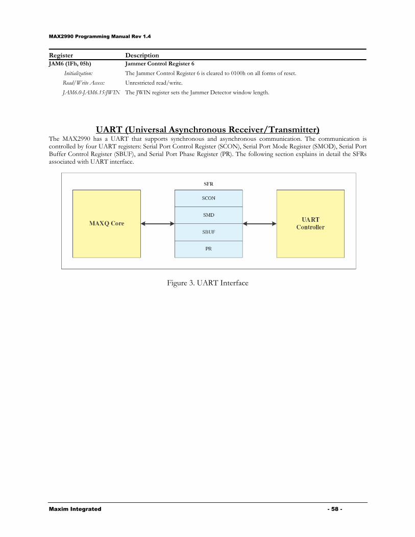
MAX2990 Programming Manual Rev 1.4
Maxim Integrated - 58 -
Register Description JAM6 (1Fh, 05h)
Initialization:
Read/Write Access:
JAM6.0-JAM6.15:JWIN
Jammer Control Register 6
The Jammer Control Register 6 is cleared to 0100h on all forms of reset.
Unrestricted read/write.
The JWIN register sets the Jammer Detector window length.
UART (Universal Asynchronous Receiver/Transmitter)
The MAX2990 has a UART that supports synchronous and asynchronous communication. The communication is controlled by four UART registers: Serial Port Control Register (SCON), Serial Port Mode Register (SMOD), Serial Port Buffer Control Register (SBUF), and Serial Port Phase Register (PR). The following section explains in detail the SFRs associated with UART interface.
Figure 3. UART Interface

MAX2990 Programming Manual Rev 1.4
Maxim Integrated - 59 -
UART SFRs
SCON (06h, 02h)
Initialization:
Read/Write Access:
Serial Port Control Register
The serial port control is cleared to 00h on all forms of reset.
Unrestricted read/write.
SCON.0: RI Receive Interrupt Flag. This bit serves as the receive interrupt flag. It is set by hardware when abyte of data is received and certain conditions are met. In mode 0, this bit is set every time a data byteis received, regardless of whether or not the FIFO is enabled. In all other modes, provided the conditions defined by SM2 (SCON.5) are met, this bit is set as follows. If the FIFO is disabled, thisbit is set every time a data byte is received. If the FIFO is enabled, this bit is set whenever a byte has been received and the FIFO has reached the capacity threshold determined by RXFT (FCON.3-FCON.2). The bit is set at the end of the 8th bit for mode 0, after the last sample of the incoming stop bit for mode 1 subject to the value of the SM2 bit, or after the last sample of RB8 for modes 2 and 3. This bit must be cleared by software once set.
SCON.1: TI Transmit Interrupt Flag. This bit serves as the transmit interrupt flag. If the FIFO is disabled, thisbit is set by hardware every time a byte of data has been transmitted. If the FIFO is enabled, this bit is set when a byte of data has been transmitted and the transmit FIFO has reached the capacitythreshold determined by TXFT (FCON.5-FCON.4).
SCON.2: RB8 9th Received Bit State. This bit identifies the state of the 9th bit of received data in serial port modes 2 and 3. When SM2 is 0, it is the state of the stop bit in mode 1. This bit has no meaning in mode 0.If the FIFO is enabled, this bit always reflects the state of the first word in the FIFO and is updated whenever software reads from the SBUF register. Software that needs to determine the state of thisbit must therefore always read SCON before reading from SBUF
SCON.3: TB8 9th Transmission Bit State. This bit defines the state of the 9th transmission bit in modes 2 and 3. If the FIFO is enabled, the state of this bit is loaded into the FIFO when software writes to the SBUFregister. Software that operates in modes 2 or 3 must therefore always write the correct state of this bit before writing to the SBUF register.
SCON.4: REN
Receive Enable.
REN_0 = 0: Serial port 0 receiver disabled.
REN_0 = 1: Serial port 0 receiver enabled for modes 1, 2 and 3.
Initiate synchronous reception for mode 0.
SCON.5: SM2
Serial Port Mode Bit 2. Setting this bit in mode 1 ignores reception if an invalid stop bit is detected. Setting this bit in mode 2 or 3 enables multiprocessor communications, and prevents the RI bit from being set and the interrupt from being asserted if the 9th bit received is 0. This bit also used to support mode 0 for clock selection:
SM2=0: Clock is divided by 12
SM2=1: Clock is divided by 4.
SCON.6: SM1
SCON.7:SM0/FE
Serial Port Mode Bit 1.
Serial Port Mode Bit 0 when FEDE is 0. When FEDE is set to 1, this bit is the Framing Error Flag that is set upon detection of an invalid stop bit. It must be cleared by software. Modification of this bit when FEDE is set has no effect on the serial mode.
Mode SM2 SM1 SM0 Function Length Period
0 0 0 0 Synchronous 8 bits 12 System clock
0 1 0 0 Synchronous 8 bits 4 System clock
1 x 1 0 Asynchronous 10 bits 64/16 Baud clock (SMOD=0/1)
2 0 0 1 Asynchronous 11 bits 64/32 System Clock (SMOD=0/1)
2 1 0 1 Asynchronous (MP) 11 bits 64/32 System clock (SMOD=0/1)
3 0 1 1 Asynchronous 11 bits 64/16 Baud clock (SMOD=0/1)
3 1 1 1 Asynchronous (MP) 11 bits 64/16 baud clock (SMOD=0/1)
MAX2990 Programming Manual Rev 1.4
Maxim Integrated - 60 -
SBUF (07h, 02h)
Initialization:
Read/Write Access:
SBUF.7 – SBUF.0
Serial Data Buffer
This buffer is cleared to 00h on all forms of reset.
Unrestricted read/write.
Serial Data Buffer 0 Bit 7:0. Data for serial port is read from or written to this location. The serial transmit and receive buffers are separate but both are addressed at this location. The depth of the buffers depends on the individual receive and transmit FIFO enables.
FCON (08h, 02h) Serial Port FIFO Control Register (8-bit Register)
Initialization: The serial port FIFO control is cleared to 00h on all forms of reset.
Read/Write Access: Unrestricted read/write.
FCON.0: FE
FIFO Enable. When set to 1, this bit enables the transmit and receive FIFO buffers. When this bitis cleared to 0, the transmit and receive buffers will be a single word deep and transmit/receive operation will be fully compatible with the 80C32.
FCON.1: OEIE
Overrun Error Interrupt Enable. When the receive FIFO is enabled (C_RFIFO_DEPTH > 1 and FEN = 1), this bit enables the Receive Overflow Error interrupt. The interrupt flag is the OE bit in FSTAT.6. If this bit is cleared, no interrupt is generated if a receive FIFO overflow occurs.
FCON.[3:2] –
RXFT[1:0]
Receive FIFO Threshold Level Bits [1:0]. When the FIFO is enabled, these bits select thethreshold for receive interrupt generation as follows:
RXFT[1:0] Rx Interrupt Condition
00 RxFIFO is Full
01 RxFIFO >= 25% full
10 RxFIFO >= 50% full
11 RxFIFO >= 75% full
When these conditions are met, a receive interrupt will be generated and the RXFAE flag will be set.
FCON.[5:4] –
TXFT[1:0]
Transmit FIFO Threshold Level Bits [1:0]. When the FIFO is enabled, these bits select thethreshold for transmit interrupt generation as follows:
TXFT[1:0] TX Interrupt Condition
00 TxFIFO is Empty
01 TxFIFO <= 25% full
10 TxFIFO <= 50% full
11 TxFIFO <= 75% full
When these conditions are met, a transmit interrupt will be generated and the TXFAE flag will be set.
FCON.6: FRF
Flush RX FIFO. Setting this bit to 1 will reset the receive FIFO pointer to 0 and reset all associatedflags to indicate the empty condition. This bit always reads 0.
FCON.7: FTF
Flush TX FIFO. Setting this bit to 1 will reset the transmit FIFO pointer to 0 and reset allassociated flags to indicate the empty condition. This bit always reads 0.
FSTAT (09h, 02h)
Initialization:
Read/Write Access:
Serial Port FIFO Status Register
The serial port status control is cleared to 00h on all forms of reset.
Unrestricted read.
FSTAT.0:RX FE Receive FIFO Empty. This flag indicates there is no data in the serial port receive FIFO.
FSTAT.1: RXFAF
Receive FIFO Almost Full. This flag indicates the serial port receive FIFO is almost full as defined by the RXFT bits in the FCON register. The setting of this flag is accompanied by a receive interrupt (if enabled).
FSTAT.2: RXFF
Receive FIFO Full. This flag indicates the serial port receive FIFO is full. If not read prior to receiving the next byte, a receive FIFO overflow will occur and the OE flag in the FCON register will be set.
FSTAT.3:TX FE Transmit FIFO Empty. This flag indicates there is no data in the serial port transmit FIFO.
FSTAT.4: TXFAE
Transmit FIFO Almost Empty. This flag indicates the serial port transmit FIFO is almost empty as defined by the TXFT bits in the FCON register. The setting of this flag is accompanied by a transmit interrupt (if enabled).
MAX2990 Programming Manual Rev 1.4
Maxim Integrated - 61 -
FSTAT.5: TXFF Transmit FIFO Full. This flag indicates the serial port transmit FIFO is full.
FSTAT.6: OE Overrun Error. When the receive FIFO is enabled (C_RFIFO_DEPTH > 1 and FEN = 1) and the FCON OEIE bit is set, this flag is set and an interrupt is generated if the Receive FIFO overflows. If this bit is set by software, a Receive FIFO overflow occurs. This bit must be cleared by software.
FSTAT.7 Reserved, read returns 0.
SMD (0Ah, 02h)
Initialization:
Read/Write Access:
Serial Port Mode Register
This register is cleared to 00h on all forms of reset.
Unrestricted read/write.
SMD.0: FEDE
Framing Error Detection Enable. This bit selects the function of SM0 (SCON.7):
FEDE = 0: SCON.7 functions as SM0 for serial port mode selection.
FEDE = 1: SCON.7 is converted to the Framing Error (FE) flag.
SMD.1: SMOD
Serial Port Baud Rate Select. The SMOD selects the final baud rate for the asynchronous mode:
SMOD=1: 16 times the baud clock for mode 1 and 3,
32 times the system clock for mode 2.
SMOD=0: 32 times the baud clock for mode 1 and 3,
64 times the system clock for mode 2.
SMD.2: ESI Enable Serial Port Interrupt. Setting this bit to 1 enables interrupt requests generated by the RI or TI flags in SCON. Clearing this bit to 0 disables the serial port interrupt.
SMD.7 – SMD.3 Reserved, read returns 0.
PR (0Bh, 02h)
Initialization:
Read/Write Access:
PR.15 – PR.0
Phase Register
The phase register is cleared to 0000h on all forms of reset.
Unrestricted read/write.
Phase Register 15:0. This register is used to load and read the 16-bit value in the phase register that determines the baud rate for the serial port.
UART Operating Modes There are four modes of UART operation (see the SCON register description). The default mode is Mode 1. Mode 0 is used to communicate in synchronous, half-duplex format. In this mode, the MAXQ generates the clock and functions as a master. Serial I/O occurs on the RXD pin, which is bi-directional data line, and the shift clock is provided on the TXD pin. The shift clock is used to shift data into and out of the microcontroller and the remote device. The shift clock may be selected to be either the clock source divided by 12 or divided by 4 as determined by the SM2 bit in the SCON register. Mode 1 is the default mode. Mode 1 is asynchronous, full duplex with a 10-bit data stream as illustrated in Figure 4. The data stream consists of a logic 0 start bit, eight data bits, and logic 1 stop bit. The data is transferred least significant bit first. The baud rate generation will be discussed in section Baud Rate Generation on page 43. The UART will begin transmission a few cycles after the first baud clock of the baud rate generator following a write to SBUF. Transmission takes place on the TXD pin. It begins with the start bit being placed on the pin, then data then is shifted out on the pin, least significant bit first, followed by the stop bit. The TI bit is set two clock cycles after the stop bit is placed on the TXD pin. All bits are shifted out at the rate determined by the baud rate generator. Once the baud rate generator is active, reception can begin at any time. The REN bit must be set to a logic 1 to enable the reception. The falling edge of a start bit on the RXD pin will begin the reception process. Data will be shifted in at the selected baud rate. At the middle the stop bit time, certain condition must be met to load SBUF with the received data in the receive shift register:
RI must be 0, and If SM2 is 0, the state of the stop bit does not matter, or If SM2 is 1, the state of the stop bit must be 1.
If these conditions are true, the SBUF will be loaded with the received byte, the RB8 bit will be loaded with the stop bit and the RI bit will be set. If these conditions are false, then SBUF and RB8 will not be loaded, the received data will be
MAX2990 Programming Manual Rev 1.4
Maxim Integrated - 62 -
lost and the RI bit will not be set. Regardless of the receive word status, the receive logic will go back to looking for a 1 to 0 transition on the RXD pin after the middle of the stop bit time. Each data bit received is sampled on the 7th, 8th, and 9th clock used by the counter, which is divided by 16. Using majority voting, two equal samples out of the three determine the logic value for each received bit. If the start bit was determined to be invalid, then the receive logic goes back to looking for a 1 to 0 transition on the RXD pin in order to start the reception again.
Figure 4. UART Mode 1
Mode 2 is asynchronous, full duplex mode with 11-bit data stream. The 11-bit data steam consists of a logic 0 start bit, eight data bits, a programmable 9th bit (can be Parity), and a logic 1 stop bit. The data is transferred least significant bit first. The transmissions occur on the TXD pin and reception on the RXD pin.
MAX2990 Programming Manual Rev 1.4
Maxim Integrated - 63 -
Mode 3 and mode 2 operation is the same, except for the baud rate generation. In Mode 2 the baud rate is generated from a system clock and is not programmable. In Mode 3 baud rate generation is programmable in the UART module like Mode 1.
UART Baud Rate Generation The baud rate generator generates the baud clock for UART modes 1 and 3. The baud clock is dependent on the system clock and the user selected phase delta value (P):
Baud Clock (for mode 1 and 3) = (P x fSYSCLK)/(217)
As illustrated in Figure 5, a 16-bit Phase Delta Register (PR) is used by the user program to select a suitable phase delta for its baud clock. When the baud rate generator is enabled, the content of the phase delta register adds to the value of the 17-bit register triggered by the system clock, essentially performing a phase accumulation. The baud clock is the result of the adder carry output to the most significant bit of the 17-bit register. Note that the baud clock is 16 times of the desired baud rate for mode 1 or 3. The trigger clock can be divided by 4 when selected by the SMOD bit.
The baud rates for mode 1 and 3 are given by the formula:
Mode 1 and 3 baud rate = (P x fSYSCLK)/(223/2(SMODx2))
where P is the phase value in the phase register. As stated in the above formula, the resulting baud rate is dependent on the phase value and the system clock frequency.
Timer B All timers in the MAX2990 are timer B type of timer. Timer B supports different input clock pre-scaling and set/reset/compare output functionality. It will also count in the range 0000h to TBR instead of TBR to 0FFFFh. This Timer will be referred to as Timer B.
Figure 5. Timer B Interface
MaxQ Core
TBCN
TBV
TBR
TBC
Timer B
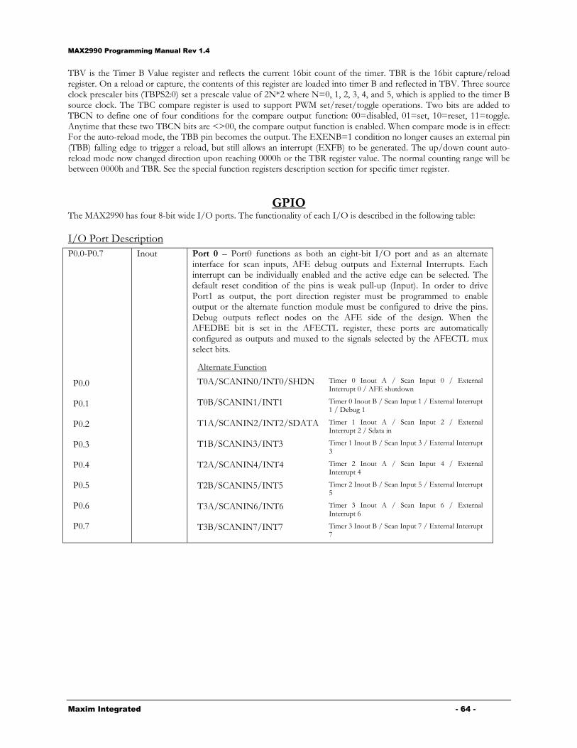
MAX2990 Programming Manual Rev 1.4
Maxim Integrated - 64 -
TBV is the Timer B Value register and reflects the current 16bit count of the timer. TBR is the 16bit capture/reload register. On a reload or capture, the contents of this register are loaded into timer B and reflected in TBV. Three source clock prescaler bits (TBPS2:0) set a prescale value of 2N*2 where N=0, 1, 2, 3, 4, and 5, which is applied to the timer B source clock. The TBC compare register is used to support PWM set/reset/toggle operations. Two bits are added to TBCN to define one of four conditions for the compare output function: 00=disabled, 01=set, 10=reset, 11=toggle. Anytime that these two TBCN bits are <>00, the compare output function is enabled. When compare mode is in effect: For the auto-reload mode, the TBB pin becomes the output. The EXENB=1 condition no longer causes an external pin (TBB) falling edge to trigger a reload, but still allows an interrupt (EXFB) to be generated. The up/down count auto-reload mode now changed direction upon reaching 0000h or the TBR register value. The normal counting range will be between 0000h and TBR. See the special function registers description section for specific timer register.
GPIO The MAX2990 has four 8-bit wide I/O ports. The functionality of each I/O is described in the following table:
I/O Port Description P0.0-P0.7
P0.0
P0.1
P0.2
P0.3
P0.4
P0.5
P0.6
P0.7
Inout Port 0 – Port0 functions as both an eight-bit I/O port and as an alternate interface for scan inputs, AFE debug outputs and External Interrupts. Each interrupt can be individually enabled and the active edge can be selected. The default reset condition of the pins is weak pull-up (Input). In order to drive Port1 as output, the port direction register must be programmed to enable output or the alternate function module must be configured to drive the pins. Debug outputs reflect nodes on the AFE side of the design. When the AFEDBE bit is set in the AFECTL register, these ports are automatically configured as outputs and muxed to the signals selected by the AFECTL mux select bits.
Alternate Function
T0A/SCANIN0/INT0/SHDN Timer 0 Inout A / Scan Input 0 / External Interrupt 0 / AFE shutdown
T0B/SCANIN1/INT1 Timer 0 Inout B / Scan Input 1 / External Interrupt 1 / Debug 1
T1A/SCANIN2/INT2/SDATA Timer 1 Inout A / Scan Input 2 / External Interrupt 2 / Sdata in
T1B/SCANIN3/INT3 Timer 1 Inout B / Scan Input 3 / External Interrupt 3
T2A/SCANIN4/INT4 Timer 2 Inout A / Scan Input 4 / External Interrupt 4
T2B/SCANIN5/INT5 Timer 2 Inout B / Scan Input 5 / External Interrupt 5
T3A/SCANIN6/INT6 Timer 3 Inout A / Scan Input 6 / External Interrupt 6
T3B/SCANIN7/INT7 Timer 3 Inout B / Scan Input 7 / External Interrupt 7

MAX2990 Programming Manual Rev 1.4
Maxim Integrated - 65 -
P1.0-P1.7
P1.0
P1.1
P1.2
P1.3
P1.4
P1.5
P1.6
P1.7
Inout Port 1 – Port1 functions as both an eight-bit I/O port and as alternate interface for serial protocols, AFE debug outputs and scan outputs. The default reset condition of the pins is weak pullup (Input). In order to drive Port1 as Output, the port direction register must be programmed to enable Output or the alternate function module must be configured to drive the pins.
Alternate Function
TXD/ SCANOUT0 MCU UART Transmit/Scan Output 0
RXD/ SCANOUT1 MCU UART Receive/Scan Output 1
I2CCLK/ SCANOUT2 I2C Clock/Scan Output 2
I2CDATA/ SCANOUT3 I2C Data/Scan Output 3
MSCLK/SCANOUT4 SPI Clk/Scan Output 4
MOSI/SCANOUT5 SPI Master Out/Scan Output 5
MISO/SCANOUT6 SPI Master In/Scan Output 6
MSSEL/SCANOUT7 SPI Master/Slave Select/Scan Output 7
P2.0-P2.7
P2.0
P2.1
P2.2
P2.3
P2.4
P2.5
P2.6
P2.7
Inout Port 2 – Port2 functions as both an eight-bit I/O port and as alternate interface for serial protocols and scan outputs. The default/reset condition of the pins is weak pullup (Input). In order to drive Port2 as Output, the port direction register must be programmed to enable Output or the alternate function module must be configured to drive the pins.
Alternate Function
GP2/SCANIN8 General Purpose 2/Scan Input 8
GP3/SCANIN9 General Purpose 3/Scan Input 9
AGC FRZ/SCANOUT8 AFE AGC freeze/Scan Output 8
UART RTS/SCANOUT9 UART RTS to jumper/Scan Output 9
UART CTS/SCANEN UART CTS to jumper/Scan Enable
AFE_CS AFE Host SPI Chip Select
AFE_SCLK AFE Serial Clock
AFE_SDOUT AFE Serial Data Out
P3.0-P3.8
P3.0
P3.1
P3.2
P3.3
P3.4
P3.5
P3.6
P3.7
P3.8
Inout Port 3 – Port3 functions as both an nine-bit I/O port and as alternate interface for the AFE. The default/reset condition of the pins is weak pullup (Input). In order to drive Port3 as Output, the port direction register must be programmed to enable Output or the alternate function module must be configured to drive the pins.
Alternate Function
AFE_TXEN AFE Transmit Enable
AFE_SDO AFE Serial Data Out
AFE_TXCLK AFE Transmit Clock
AFE_RXCLK AFE Receive Clock
AFE_SDI AFE Serial Data In
AFE_RXEN AFE Receive Enable
AFE_RSTN AFE Reset
AFE_GP1 AFE General-Purpose Pin 1
AFE_GP0 AFE General-Purpose Pin 0
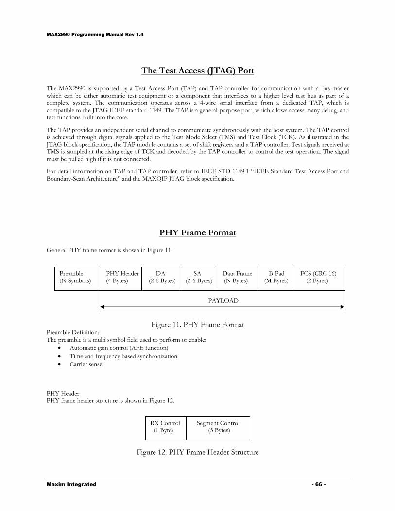
MAX2990 Programming Manual Rev 1.4
Maxim Integrated - 66 -
The Test Access (JTAG) Port
The MAX2990 is supported by a Test Access Port (TAP) and TAP controller for communication with a bus master which can be either automatic test equipment or a component that interfaces to a higher level test bus as part of a complete system. The communication operates across a 4-wire serial interface from a dedicated TAP, which is compatible to the JTAG IEEE standard 1149. The TAP is a general-purpose port, which allows access many debug, and test functions built into the core.
The TAP provides an independent serial channel to communicate synchronously with the host system. The TAP control is achieved through digital signals applied to the Test Mode Select (TMS) and Test Clock (TCK). As illustrated in the JTAG block specification, the TAP module contains a set of shift registers and a TAP controller. Test signals received at TMS is sampled at the rising edge of TCK and decoded by the TAP controller to control the test operation. The signal must be pulled high if it is not connected.
For detail information on TAP and TAP controller, refer to IEEE STD 1149.1 “IEEE Standard Test Access Port and Boundary-Scan Architecture” and the MAXQIP JTAG block specification.
PHY Frame Format
General PHY frame format is shown in Figure 11.
Figure 11. PHY Frame Format Preamble Definition: The preamble is a multi symbol field used to perform or enable:
Automatic gain control (AFE function) Time and frequency based synchronization Carrier sense
PHY Header: PHY frame header structure is shown in Figure 12.
Figure 12. PHY Frame Header Structure
Preamble PHY Header DA SA Data Frame B-Pad FCS (CRC 16)(N Symbols) (4 Bytes) (2-6 Bytes) (2-6 Bytes) (N Bytes) (M Bytes) (2 Bytes)
PAYLOAD
RX Control Segment Control (1 Byte) (3 Bytes)

MAX2990 Programming Manual Rev 1.4
Maxim Integrated - 67 -
PHY Frame Header Description
Field Byte Bit
Number Bits Description
7 1 Channel Quality Request ‘1’ – Channel Quality requested; ‘0’ – Disabled;
6 1 Encryption: ‘1’ – Enabled; ‘0’ – Disabled;
5-3 3 Encryption Key Select (EKS) Value from 0 to 7
2 1 ARQ type: ‘1’ – ACK requested; ‘0’ – ACK disabled;
1 1 Priority: ‘1’ – High; ‘0’ – Normal;
RX Control
0
0 1 Addressing mode: ‘1’ – 48-bit address; ‘0’ – 16-bit address
1 7-0 8 Sequence number (SN) 2 7 1 Last Segment Flag (LSF) 2 6-3 4 Segment Count (SC) 2 2-0 3 Segment Length, SL[10-8]
Segment Control
3 7-0 8 Segment Length, SL[7-0] Sequence Number: This field contains 8-bit sequence number (SN) that is to be incremented for each new Service Block to be transmitted. Segment Length: The 11-bit Segment Length (SL) field contains the number of bytes in the Data Frame. The Segment Length is required to properly remove B-Padding. Last Segment Flag: The one-bit last segment flag shall be set to 0b1 if the current segment is the last (or only) segment of the Service Block. Segment Count:: The 4-bit Segment Count field contains the incrementing sequential count of the transmitted segment(s) and is used by the segmentation and reassembly algorithm. The first segment is indicated by SC = 0b0000. Destination Address: The Destination Address field specifies the station(s)for which the frame is intended. It may be an individual or multicast (including broadcast) address. Source Address: The Source Address field specifies the station sending the frame. Data Frame: This variable length field carries the data the MAC was requested to deliver. It may be encrypted depends on “Encryption Enable” flag in the Header. Block Pad (B-PAD): A frame may require padding to ensure that the payload fills an entire PHY transmission block. Zeros are padded between the Data and the 16-bit CRC at the end of a frame. B-PAD shall only be used in the last frame.

MAX2990 Programming Manual Rev 1.4
Maxim Integrated - 68 -
MAC Code
The MAX2990 Digital Transceiver chip combines both the Physical (PHY) and Media Access Control (MAC) layers using 16-bit MAXQ microprocessor. The MAC software is developed using “IAR Embedded Workbench® for MAXQ” from IAR Systems. The MAC software source code is provided with the MAX2990 Evaluation Kit package. This section gives a brief introduction about IAR Embedded Workbench and explains the MAC programmability of MAX2990. Following are the features of IAR Embedded Workbench for MAXQ:
The highly optimizing IAR MAXQ C compiler The powerful IAR MAXQ assembler The IAR XLINK Linker™ The IAR XAR Library Builder™ and the IAR XLIB Librarian™ A powerful editor A project manager A command line build utility IAR C-SPY® debugger
For a detailed description, refer to the online documentation of IAR Embedded Workbench at www.iar.com.
Figure 13. IAR Embedded Workbench IDE for MAX2990
Changing Transmitter Gain The transmitter gain can be chose among –10dB, -6dB, -4dB, 0dB, 4dB, and 6dB. The transmitter gain can be changed in ‘menue.c’ source file.
Workspace Window Editor
Window
IAR Embedded Workbench and C-SPY are registered trademarks of IAR Systems AB. IAR XLINK Linker, IAR XAR Library Builder, and the IAR XLIB Librarian are trademarks of IAR Systems AB.
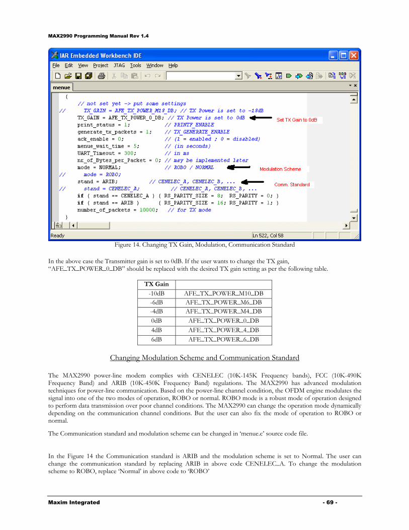
MAX2990 Programming Manual Rev 1.4
Maxim Integrated - 69 -
Figure 14. Changing TX Gain, Modulation, Communication Standard
In the above case the Transmitter gain is set to 0dB. If the user wants to change the TX gain, “AFE_TX_POWER_0_DB” should be replaced with the desired TX gain setting as per the following table.
TX Gain -10dB AFE_TX_POWER_M10_DB -6dB AFE_TX_POWER_M6_DB -4dB AFE_TX_POWER_M4_DB 0dB AFE_TX_POWER_0_DB 4dB AFE_TX_POWER_4_DB 6dB AFE_TX_POWER_6_DB
Changing Modulation Scheme and Communication Standard The MAX2990 power-line modem complies with CENELEC (10K-145K Frequency bands), FCC (10K-490K Frequency Band) and ARIB (10K-450K Frequency Band) regulations. The MAX2990 has advanced modulation techniques for power-line communication. Based on the power-line channel condition, the OFDM engine modulates the signal into one of the two modes of operation, ROBO or normal. ROBO mode is a robust mode of operation designed to perform data transmission over poor channel conditions. The MAX2990 can change the operation mode dynamically depending on the communication channel conditions. But the user can also fix the mode of operation to ROBO or normal.
The Communication standard and modulation scheme can be changed in ‘menue.c’ source code file.
In the Figure 14 the Communication standard is ARIB and the modulation scheme is set to Normal. The user can change the communication standard by replacing ARIB in above code CENELEC_A. To change the modulation scheme to ROBO, replace ‘Normal’ in above code to ‘ROBO’

MAX2990 Programming Manual Rev 1.4
Maxim Integrated - 70 -
MAC Functions Description The MAX2990 receives the raw data from UART or generate data inside MAC code. If data is from UART, MAC code gets it from ISR in isr.c – serial port interrupt service routine. The UART initialization is implemented in ‘uart.c’ source code file. The MAX2990 composes the power-line packet (see Figure 11 for frame format) and encrypts the data payload if DES is enabled. The encryption implementation functions are in ‘des.c’ source code file. Once the power-line packet is ready, MAC indicates PHY that the packet is ready to transmit over the power line. On the receive side MAC get data from the power line, analyze the packet header, decrypt the data, and send the data payload to the UART.
Main function example flowchart
This example program initializes clock, MAC, PHY, MAC buffer, encryption key, UART, timer, LED and CSMA, then runs five tasks MAC_transmit, PHY_transmit, PHY_receive, MAC_receive, and LED control one by one continually.
main
MAC_transmit
PHY_transmit
PHY_receive
EXIT
init clock, MAC, PHY,MAC buffer, encryptionkey, UART, timer, LED,
CSMA
MAC_receive
LED control
System Init
Functions in this section are used to initialize MAC and PHY, peripherals. CLK_init() This function sets MAQX(32 MHz), AFE(19.2 MHz) and PHY(16 MHz) clocks.

MAX2990 Programming Manual Rev 1.4
Maxim Integrated - 71 -
Syntax void CLK_init() Parameters None Return None Limitation None UART_init() This function configures PD2(module 0, register 18) for CTS, RTS of UART. It also configures UART asynchronous mode, buffer, baud rate and interrupt, set phase register. The formula for baud rate and phase value P in phase register is: P = Baud rate x (223/2(SMODx2))/fSYSCLK, SMOD can be 0 or 1. Syntax void UART_init(UINT16 baud) Parameters UINT16 baud - baud rate for UART Return None Limitation None DES_key_init() This function initializes DES key using network encryption key parameter. Syntax void DES_key_init(UINT16 *nekPtr) Parameters UINT16* nekPtr – DES key Return None Limitation None MAC_init() This function sets phyFrameDataSize based on supported standard and mode. phyFrameDataSize = (RS block size) - (RS parity size) - (CRC16 size) - (Header size) Syntax void MAC_init(ENUM_PHY_STANDARD standard, ENUM_FEC_MODE fecMode) Parameters ENUM_PHY_STANDARD standard - PHY supported standard (FCC, ARIB, CENELEC_A, CENELEC_B,
CENELEC_C, CENELEC_BC) default FCC
MAX2990 Programming Manual Rev 1.4
Maxim Integrated - 72 -
ENUM_FEC_MODE fecMode - FEC Normal or ROBO mode Return None Limitation None MAC_buffer_init() This function initializes MAC TX/RX buffers. There are two TX buffers and two RX buffers. While data in one buffer is being processed, the other buffer can be used to get more data. It uses the following structure for the buffer: typedef struct { UINT16 dSize; //data size UINT8 hSize; //header size UINT8 *dPtr; //data pointer UINT8 *hPtr; //header pointer } PACKET_STR; Syntax void MAC_buffer_init(void) Parameters None Return None Limitation None PHY_init() This function sets/configures the following PHY parameters/registers:
1. Jammer detector, jammer canceller, jammer control register 2. High pass filter 3. AGC control register 4. CRC16 5. DC block register 6. TX FEC mode, TX pre-emphasis filter 7. Channel estimation threshold. 8. Modulator/Demodulator control registers 9. Symbol synchronizer control register 10. Buffer manager control register 11. Device address for filtering 12. Preamble parameters 13. FEC control registers 14. Interleaver control register 15. RMS block 16. Analog PGA. 17. PHY, Data manager and DES interrupts.
Syntax void PHY_init(ENUM_PHY_STANDARD standard, ENUM_FEC_MODE fecMode) Parameters
MAX2990 Programming Manual Rev 1.4
Maxim Integrated - 73 -
ENUM_PHY_STANDARD standard - PHY supported standard ENUM_FEC_MODE fecMode - FEC Normal or ROBO mode Return None Limitation None TIMER_init() This function sets timer registers and enable timer interrupt module. Syntax void TIMER_init(void) Parameters None Return None Limitation None LED_init() This function enables LED, turns on link LED, and turns off activity and collision LED. These LEDs’ on/off are controlled through PO0 (module0, register0), bit 5,6,7. Direction is controlled by PD0 (module0, register 16) bit 5,6,7. Syntax void LED_init(void) Parameters None Return None Limitation None CSMA_init() This function sets initial CSMA seed based on unique 48-bit device address. Syntax void CSMA_init(void) Parameters None Return None Limitation None
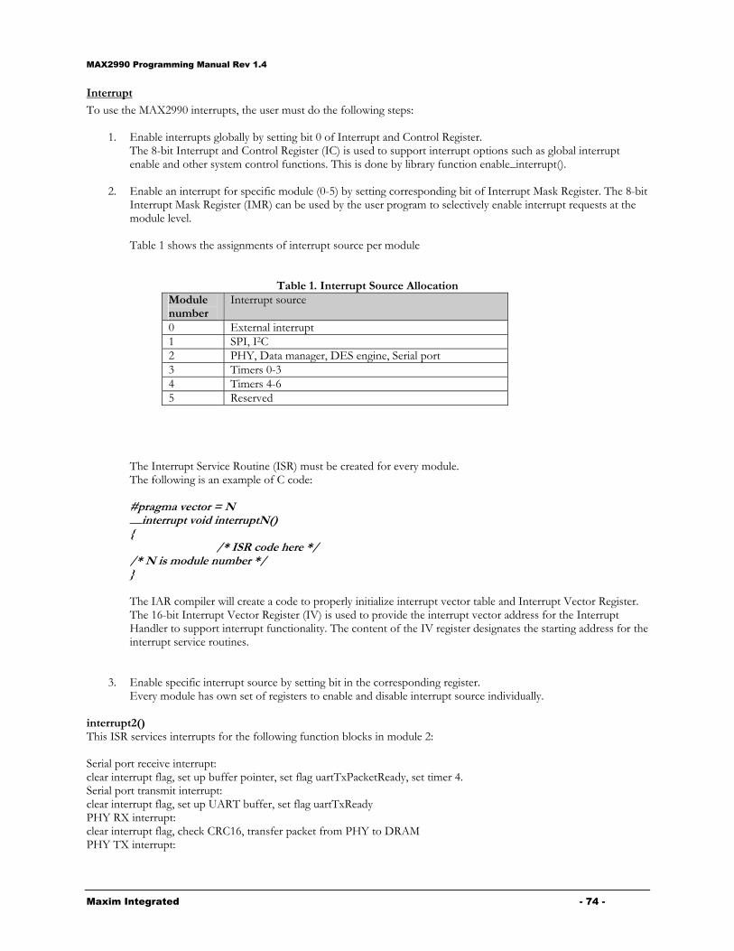
MAX2990 Programming Manual Rev 1.4
Maxim Integrated - 74 -
Interrupt
To use the MAX2990 interrupts, the user must do the following steps:
1. Enable interrupts globally by setting bit 0 of Interrupt and Control Register. The 8-bit Interrupt and Control Register (IC) is used to support interrupt options such as global interrupt enable and other system control functions. This is done by library function enable_interrupt().
2. Enable an interrupt for specific module (0-5) by setting corresponding bit of Interrupt Mask Register. The 8-bit
Interrupt Mask Register (IMR) can be used by the user program to selectively enable interrupt requests at the module level.
Table 1 shows the assignments of interrupt source per module
Table 1. Interrupt Source Allocation Module number
Interrupt source
0 External interrupt 1 SPI, I2C 2 PHY, Data manager, DES engine, Serial port 3 Timers 0-3 4 Timers 4-6 5 Reserved
The Interrupt Service Routine (ISR) must be created for every module. The following is an example of C code:
#pragma vector = N __interrupt void interruptN() { /* ISR code here */ /* N is module number */ }
The IAR compiler will create a code to properly initialize interrupt vector table and Interrupt Vector Register. The 16-bit Interrupt Vector Register (IV) is used to provide the interrupt vector address for the Interrupt Handler to support interrupt functionality. The content of the IV register designates the starting address for the interrupt service routines.
3. Enable specific interrupt source by setting bit in the corresponding register. Every module has own set of registers to enable and disable interrupt source individually.
interrupt2() This ISR services interrupts for the following function blocks in module 2: Serial port receive interrupt: clear interrupt flag, set up buffer pointer, set flag uartTxPacketReady, set timer 4. Serial port transmit interrupt: clear interrupt flag, set up UART buffer, set flag uartTxReady PHY RX interrupt: clear interrupt flag, check CRC16, transfer packet from PHY to DRAM PHY TX interrupt:

MAX2990 Programming Manual Rev 1.4
Maxim Integrated - 75 -
clear interrupt flag, switch to RX mode after sending ACK. Data Manager TX interrupt: clear interrupt flag, prepare to receive data from UART Data Manager RX interrupt: clear interrupt flag. If ACK required, switch to TX mode, sending ACK. DES interrupt: clear interrupt flag PHY Carrier Sense Interrupt: clear interrupt flag ACK interrupt: clear interrupt, switch to normal RX mode to receive the next packet. Syntax __interrupt void interrupt2() Parameters None Return None Limitation None interrupt3() This ISR services interrupts for the following function blocks in module 3: Timer 0 interrupt: clear interrupt flag, check medium state for CSMA. Timer 1 interrupt: clear interrupt flag Timer 2 interrupt: clear interrupt flag Timer 3 interrupt: clear interrupt flag, enable data rate calculation. Syntax __interrupt void interrupt3() Parameters None Return None Limitation None interrupt4() This ISR services interrupts for the following function block in module 4: Timer 4 interrupt: clear interrupt flag, configure data buffer, set flag uartTxPacketReady, switch buffer Syntax __interrupt void interrupt4()
MAX2990 Programming Manual Rev 1.4
Maxim Integrated - 76 -
Parameters None Return None Limitation None
LED
These functions control the LED activities. ACT_LED_control() This function controls LED to show RX/TX activities, when there is new TX/RX packet, the LED is on. There is also a counter for LED. When there is no TX/RX packet, and the counter decreases to 0, turn off the activity LED. Syntax void ACT_LED_control(void) Parameters None Return None Limitation None COLL_LED_control() This function controls LED to show collisions, when there are retransmission or CRC16 error of the received packet, turn on collision LED. When there is no collisions and CRC16 error, and collLedState counter reaches 0, turn off the collision LED. Syntax void COLL_LED_control(void) Parameters None Return None Limitation None
Timer
These functions set up, start and stop timer. TIMER_start() This function starts the timer by setting the timer control register bit TRB.

MAX2990 Programming Manual Rev 1.4
Maxim Integrated - 77 -
Syntax void TIMER_start(UINT8 timer) Parameters UNIT8 timer – the timer number that will be started. Return None Limitation None TIMER_stop() This function stops the timer by clearing the timer control register bit TRB. Syntax void TIMER_stop(UINT8 timer) Parameters None Return None Limitation None TIMER_load() This function sets auto reload value for the timer. Syntax void TIMER_load(UINT8 timer, UINT16 value) Parameters UNIT8 timer – the timer number that will be reloaded. UNIT8 value – the value that reloaded into timer TBR register. Return None Limitation None
Encryption
DES algorithm is used for encryption. It is implemented in hardware. The following function is the API to control this hardware. DES_start() This function encrypts/decrypts data. Syntax void DES_start(UINT16 *dataPtr, UINT16 blockCount, UINT16 mode)

MAX2990 Programming Manual Rev 1.4
Maxim Integrated - 78 -
Parameters UINT16* dataPtr - data address in word mode UINT16 blockCount - nymber of cypher blocks (4 bytes) INT16 mode - DES engine mode: 0 - decryption, 1 – encryption Return None Limitation DataPtr is in word mode, Size of the data should be multiple of 4 bytes.
MAC functions
These functions process packet at MAC layer. MAC_transmit() This function checks flag uartTxPacketReady, If the flag is 1 this function prepares packet header and data buffer for transmission, encrypts it if required. Syntax void MAC_transmit(void) Parameters None Return None Limitation None

MAX2990 Programming Manual Rev 1.4
Maxim Integrated - 79 -
M A C T ransm it
C om pose packet
uartTxP acketR eady=1
E ncrypt packetpayload
E N D
N O
Y E S
TX packet isready
MAC_receive() This function processes received packet from physical layer. It checks flag macRxPacketReady. It decrypts if required, analyzes header, and checks bit error, Syntax void MAC_receive(void) Parameters None Return None Limitation None

MAX2990 Programming Manual Rev 1.4
Maxim Integrated - 80 -
MAC_receive
macRxPacketReadyNo
Yes
Process Packet
Decrypt
EXIT
Send packet toUART
CRC32 error
No
Yes
PHY functions
These functions configure different PHY modes, and TX/RX at PHY layer. PHY_tx_mode() This function configures PHY to transmit mode. Syntax void PHY_tx_mode(void) Parameters None Return None Limitation None PHY_rx_mode() This function configures PHY to receive mode. Syntax void PHY_rx_mode(void)
MAX2990 Programming Manual Rev 1.4
Maxim Integrated - 81 -
Parameters None Return None Limitation None PHY_fec_mode() This function configures PHY FEC mode. Syntax void PHY_fec_mode(ENUM_FEC_MODE fecMode) Parameters ENUM_FEC_MODE fecMode - FEC Normal or ROBO mode Return None Limitation None PHY_rx_reset() This function resets PHY RX circuit. Syntax void PHY_rx_reset(void) Parameters None Return None Limitation None PHY_tx_reset() This function resets PHY TX circuit. Syntax void PHY_tx_reset(void) Parameters None Return None Limitation None PHY_receive()

MAX2990 Programming Manual Rev 1.4
Maxim Integrated - 82 -
This function checks packet on PHY, if packet is received it sets flag macRxPacketReady. It also checks packet header, and removes redundant packet based on sequence number from header. Syntax void PHY_receive(void) Parameters None Return None Limitation None
PHY_receive
phyRxPacketReady=1No
Yes
set macRxPacketReady flag
compute RMS
EXIT
redundant packetNewSN=OldSN
update oldsequence number
drop redundant packet,clear
macRxPacketReadyflag
Yes
No
PHY_transmit() This function checks flag macTxPacketReady. It configures PHY to TX mode. Running CSMA if required, checking ACK if required. If no ACK is received, it retransmits the packet. Syntax void PHY_transmit(void) Parameters None

MAX2990 Programming Manual Rev 1.4
Maxim Integrated - 83 -
Return None Limitation None
Transmit Packet
ResponseTime Expired?
RetransmitPacket
END
ReceivedACK?
Number ofRetries expired?
DiscardPacket
NOYES
YES NO
YES NO
YES
NOmacTxPacketReady=1
PHY Transmit
MAXIM_AFE_config() This function configures Maxim MAX1077 ADC/MAX5144 DAC for discrete AFE solution or MAX2991. Syntax void MAXIM_AFE_config(void) Parameters None
MAX2990 Programming Manual Rev 1.4
Maxim Integrated - 84 -
Return None Limitation None
Channel Estimation
Channel_estimation() This function sets registers for channel estimation, reads pseudo SNR value for received packet. Syntax void Channel_estimation(void) Parameters None Return None Limitation None
CSMA(Carrier Sense Multiple Access)
CSMA_random_backoff() This function sets CSMA random backoff number, and loads backoff timeout to timer 0. Syntax void CSMA_random_backoff(void) Parameters None Return None Limitation None
Miscellaneous
These functions are used for testing and debugging. MAC_transmit_print() This function outputs TX statistical information: phyTxPacket, ackReceived, txRetransmit, dataRate. Syntax void MAC_transmit_print(void) Parameters None Return None
MAX2990 Programming Manual Rev 1.4
Maxim Integrated - 85 -
Limitation None MAC_receive_print() This function outputs RX statistical information: macRxPacket, crc16Error, crc32Error, dataRate. Syntax void MAC_receive_print() Parameters None Return None Limitation None delay() This function implements delay. Syntax void delay(UINT32 n) Parameters UINT32 n – the delay cycle Return None Limitation None TX_packet_generate() This function generates TX packet for test. There are two types of data payload: all ones and “+”, “-“ alternately. Syntax void TX_packet_generate(void) Parameters None Return None Limitation None RMS_read() This function gets RMS value for received packet. Syntax void RMS_read(void) Parameters None

MAX2990 Programming Manual Rev 1.4
Maxim Integrated - 86 -
Return None Limitation None
Macros description
This section describes global definitions in global.h ALL_ONES: If it is defined all data inside test TX packet will be 0xFF. RMS_ENABLE: It enables the RMS calculation. CH_EST: It enables channel estimation. CSMA_ENABLE: It enables CSMA. APGA_ENABLE: It controls the outside analog AGC, it uses three bits to control the gain. It must be disabled for MAX2991 AFE. BER_FER_ENABLE: It enables bit error and frame error calculation for receiver. DES_ENABLE: It enables data payload encryption/decryption. CRC32_ENABLE: It enables CRC32 calculation. DES_OPERATION_MODE: Define it as 0 means DES and CRC32 disabled. Define it as 1 means CRC32 operation only, no DES. Define it as 2 means DES operation only, no CRC32. Define it as 3 means DES and CRC32 enabled. ADDR_FILTER_ENABLE: It enables address filtering on receiver. Destination address is part of the packet header. CRC16_FILTER_ENABLE: It enables CRC16 filtering. If receive packet is corrupted it will be ignored by PHY. The following code defines sizes of header, crc16 and crc32 in bytes. #define HEADER_SIZE 16 #define CRC16_SIZE 2 #define CRC32_SIZE 4 ENUM_PHY_STANDARD: This enumerator contains PHY supported standards: FCC, ARIB, CENELEC_A, CENELEC_B, CENELEC_C, and CENELEC_BC. ENUM_FEC_MODE: This enumerator contains PHY modes: NORMAL, ROBO, and AUTO.

MAX2990 Programming Manual Rev 1.4
Maxim Integrated - 87 -
Global variables description
This section describes global variables in main.c const UINT16 NEK[4] network encryption key const UINT8 DA[6] destination address const UINT8 SA[6] source address const UINT8 deviceAddress[6] device address to filter the received packet.