max121 308ksps adc ith dsp interace an 78b sinad · general description the max121 is a complete,...
TRANSCRIPT

General DescriptionThe MAX121 is a complete, BiCMOS, serial-output, sampling 14-bit analog-to-digital converter (ADC) that com bines an on-chip track/hold and a low-drift, low-noise, buried-zener voltage reference with fast conversion speed and low power consumption. The throughput rate is as high as 308k samples per second (ksps). The full-scale analog input range is ±5V.The MAX121 utilizes the successive-approximation archi-tecture with a high-speed DAC to achieve both fast conversion speeds and low-power operation. Operating with +5V and -12V or -15V power supplies, power con-sumption is only 210mW.The MAX121 can be directly interfaced to the serial port of most popular digital-signal processors, and comes in space-saving 16-pin DIP and SO and smaller 20-pin SSOP packages. The MAX121 operates with TTL- and CMOS-compatible clocks in the frequency range from 1.1MHz to 5.5MHz. All logic inputs and outputs are TTL - and CMOS-compatible. This data sheet includes applica-tion notes for easy interface to TMS320, µPD77230, and ADSP2101 digital-signal processors, as well as µPs using the Motorola SPI and QSPI interface standards.
Applications Digital Signal Processing Audio and Telecom Processing Speech Recognition and Synthesis DSP Servo Control Spectrum Analysis
Benefits and Features 14-Bit Resolution 2.9µs Conversion Time/308ksps Throughput 400ns Acquisition Time Low Noise and Distortion
• 78d8 SINAD • -85dB THD
±5V Bipolar Input Range, Overvoltage Tolerant to ±15V
210mW Power Dissipation Continuous-Conversion Mode Available 30ppm/°C, -5V Internal Reference Interfaces to DSP Processors 16-Pin DIP and SO Packages,
20-Pin SSOP Package
Ordering Information appears at end of data sheet.
For related parts and recommended products to use with this part, refer to www.maximintegrated.com/MAX121.related.
DAC
SAR
AIN
3kΩ
TRACK/HOLD
CONTROL LOGIC
MAX121 BUFFER
7pF
REFERENCE
SAMPLINGCOMPARATOR
-5V
VDD
VSS
AGND
DGND
SDATA
SCLK
FSTRT
SFRM
CONVST CS MODE INVCLK INVFRM
3kΩ
VREF
CLIKIN
MAX121 308ksps ADC with DSP Interface and 78dB SINAD
19-0108; Rev 3; 1/12
Functional Diagram
EVALUATION KIT AVAILABLE

VDD to DGND . ........................................................-0.3V to +6VVSS to DGND ........................................................+0.3V to -17VAIN to AGND .......................................................................±15VAGND to DGND .................................................................±0.3VDigital Inputs to DGNO ............................. -0.3V to (VDD + 0.3V)(CS, CONVST, MODE, CLKIN, INVCLK, INVFRM)Digital Outputs to DGND ......................... +0.3V to (VDD + 0.3V)(SFRM, FSTRT, SCLK, SDATA)
Continuous Power Dissipation (TA = +70°C) 16-Pin PDIP (derate 10.53mW/°C above +70°C) .........842mW 16-Pin Wide SO (derate 9.52mW/°C above +70°C) .....762mW 20-Pin SSOP (derate 8.00mW/°C above +70°C)..........640mWOperating Temperature Ranges MAX121C_ ..........................................................0°C to +70°C MAX121E_ ...................................................... -40°C to +85°CStorage Temperature Range ........................... -65°C to + 160°CLead Temperature (soldering, 10s) .................................+300°CSoldering Temperature (reflow) .......................................+260°C
(VDD = 4.75V to 5.25V, VSS = -10.8V to -15.75V, fCLK = 5.5MHz, TA = TMIN to TMAX, unless otherwise noted.)
PARAMETER SYMBOL CONDITIONS MIN TYP MAX UNITSDYNAMIC PERFORMANCE (fS = 308kHz, VAIN = 10VP-P, 50kHz)
Signal-to-Noise Ratio SINAD Including distortionMAX121C 75 78
dBMAX121E 73 77
Total Harmonic Distortion THD First five harmonics -85 -77 dB
Spurious-Free Dynamic Range SFDR 77 86 dB
ACCURACYResolution RES 14 Bits
Differential Nonlinearity (Note 1) DNL 12 bits no missing codes over temperature range ±1.5 LSB
Integral Nonlinearity INL ±2 LSB
Bipolar Zero ErrorCode 00..00 to 00..01 transition, near VAIN = 0V ±10 mV
Temperature drift ±1 ppm/°C
Full-Scale Error (Notes 1, 2) Including reference; adjusted for bipolar zero error; TA = +25°C ±0.2 %
Full-Scale Temperature Drift Excluding reference ±1 ppm/°C
Power-Supply RejectionVDD only, 5V ±5% ±1/2 ±2
LSBVSS only, -12V ±10% ±1 ±2
VSS only, -15V ±5% ±1 ±2
ANALOG INPUTInput Range -5 +5 V
Input Current VAIN = 5V (RIN approximately 6kW to REF) 2.5 mA
Input Capacitance (Note 3) 10 pF
Full-Power Bandwidth 1.5 MHz
MAX121 308ksps ADC with DSP Interface and 78dB SINAD
www.maximintegrated.com Maxim Integrated 2
Absolute Maximum Ratings
Stresses beyond those listed under “Absolute Maximum Ratings” may cause permanent damage to the device. These are stress ratings only, and functional operation of the device at these or any other conditions beyond those indicated in the operational sections of the specifications is not implied. Exposure to absolute maximum rating conditions for extended periods may affect device reliability.
Electrical Characteristics

(VDD = 4.75V to 5.25V, VSS = -10.8V to -15.75V, fCLK = 5.5MHz, TA = TMIN to TMAX, unless otherwise noted.)
PARAMETER SYMBOL CONDITIONS MIN TYP MAX UNITSREFERENCEOutput Voltage No external load, VAIN = 5V, TA = +25°C -5.02 -4.98 V
External Load Regulation 0mA < ISINK < 5mA, VAIN = 0V 5 mV
Temperature Drift (Note 4) ±30 ppm/°C
CONVERSION TIMESynchronous tCONV 16 tCLK 2.91 µs
Clock Frequency fCLK 0.1 5.5 MHz
DIGITAL INPUTS (CLKIN, CONVST, CS)Input High Voltage VIH 2.4 V
Input Low Voltage VIL 0.8 V
Input Capacitance (Note 3) 10 pF
Input Current VDD = 0V or VDD ±5 µA
DIGITAL OUTPUTS (SCLK, SDATA, FSTRT, SFRM)Output Low Voltage VOL ISINK = 1.6mA 0.4 V
Output High Voltage VOH ISOURCE = 1mA VDD - 0.5 V
Leakage Current ILKG VOUT = 0V or VDD ±5 µA
Output Capacitance (Note 3) 10 pF
POWER REQUIREMENTSPositive Supply Voltage VDD By supply rejection test 4.75 5.25 V
Negative Supply Voltage VSS By supply rejection test -10.8 -15.75 V
Positive Supply Current IDDVDD = 15.25V, VSS = -15.75V, VAIN = 0V, VCS = VCONVST = VMODE = 5V 9 15 mA
Negative Supply Current ISSVDD = 15.25V, VSS = -15.75V, VAIN = 0V, VCS = VCONVST = VMODE = 5V 14 20 mA
Power Dissipation VDD = 15.25V, VSS = 12V, VAIN = 0V, VCS = VCONVST = VMODE = 5V 213 315 mW
MAX121 308ksps ADC with DSP Interface and 78dB SINAD
www.maximintegrated.com Maxim Integrated 3
Electrical Characteristics (continued)

(VDD = 5V, VSS = -12V or -15V, TA = TMIN to TMAX, unless otherwise noted.) (Note 5)
Note 1: These tests are performed at VDD = +5V. VSS = -15V. Operation over supply is guaranteed by supply-rejection tests.Note 2: Ideal full-scale transition is at +5V - 3/2 LSB = +4.9991V adjusted for offset error.Note 3: Guaranteed, not tested.Note 4: Temperature drift is defined as the change in output voltage from +25°C to TMIN or TMAX. It is calculated as
TC = (ΔVREF/VREF)/ΔT. Note 5: Control inputs specified with tr = tf = 5ns (10% to 90% of +5V) and timed from a voltage level of 1.6V. Output delays are
measured to +0.8V if going low, or +2.4V if going high. For a data-hold time, a change of 0.5V is measured. See Figures 4 and 5 for load circuits.
Note 6: Guaranteed, not tested.
PARAMETER SYMBOL CONDITIONSTA = +25°C MAX121C/E MAX121M
UNITSMIN TYP MAX MIN TYP MAX MIN TYP MAX
CONVST Pulse Width (Note 6)
tCW 20 30 35 ns
Data-Access Time tDA CL = 50pF 25 50 65 80 ns
Data-Hold Time tDH 25 50 65 80 ns
CLKIN to SCLK tCD CL = 50pF 40 65 85 105 ns
SCLK to SDATA Skew tSC CL = 50pF ±65 ±80 ±100 ns
SCLK to SFRM or FSTRT Skew tSC CL = 50pF ±25 ±35 ±40 ns
Acquisition Time (Note 6) tAQ 400 400 400 ns
Aperture Delay tAP 10 ns
Aperture Jitter 30 ns
Clock Setup/Hold Time tCK 10 50 10 50 10 50 ns
MAX121 308ksps ADC with DSP Interface and 78dB SINAD
www.maximintegrated.com Maxim Integrated 4
Timing Characteristics
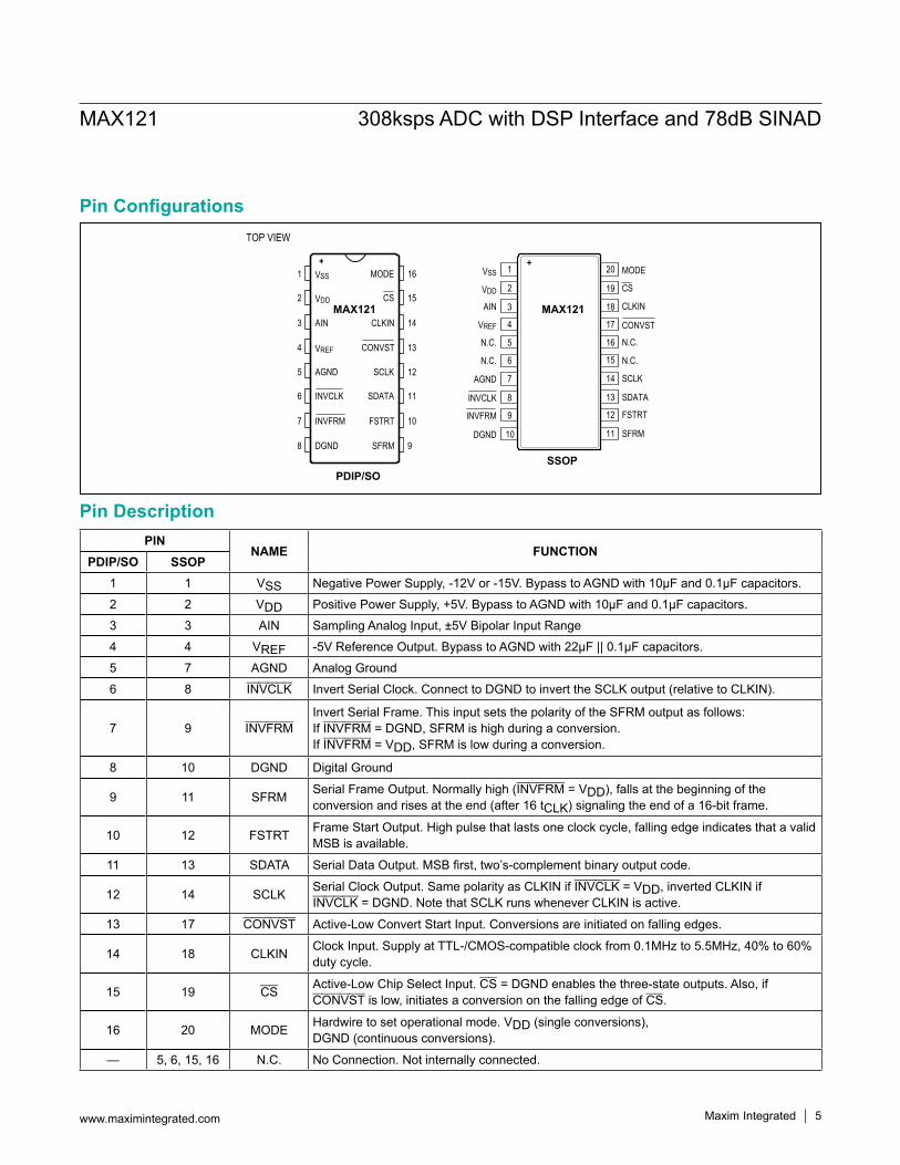
PINNAME FUNCTION
PDIP/SO SSOP1 1 VSS Negative Power Supply, -12V or -15V. Bypass to AGND with 10µF and 0.1µF capacitors.
2 2 VDD Positive Power Supply, +5V. Bypass to AGND with 10µF and 0.1µF capacitors.
3 3 AIN Sampling Analog Input, ±5V Bipolar Input Range
4 4 VREF -5V Reference Output. Bypass to AGND with 22µF || 0.1µF capacitors.
5 7 AGND Analog Ground
6 8 INVCLK Invert Serial Clock. Connect to DGND to invert the SCLK output (relative to CLKIN).
7 9 INVFRMInvert Serial Frame. This input sets the polarity of the SFRM output as follows:If INVFRM = DGND, SFRM is high during a conversion.If INVFRM = VDD, SFRM is low during a conversion.
8 10 DGND Digital Ground
9 11 SFRM Serial Frame Output. Normally high (INVFRM = VDD), falls at the beginning of the conversion and rises at the end (after 16 tCLK) signaling the end of a 16-bit frame.
10 12 FSTRT Frame Start Output. High pulse that lasts one clock cycle, falling edge indicates that a valid MSB is available.
11 13 SDATA Serial Data Output. MSB first, two’s-complement binary output code.
12 14 SCLK Serial Clock Output. Same polarity as CLKIN if INVCLK = VDD, inverted CLKIN if INVCLK = DGND. Note that SCLK runs whenever CLKIN is active.
13 17 CONVST Active-Low Convert Start Input. Conversions are initiated on falling edges.
14 18 CLKIN Clock Input. Supply at TTL-/CMOS-compatible clock from 0.1MHz to 5.5MHz, 40% to 60% duty cycle.
15 19 CS Active-Low Chip Select Input. CS = DGND enables the three-state outputs. Also, if CONVST is low, initiates a conversion on the falling edge of CS.
16 20 MODE Hardwire to set operational mode. VDD (single conversions), DGND (continuous conversions).
— 5, 6, 15, 16 N.C. No Connection. Not internally connected.
AIN
VREF CONVST
1
2
16
15
VSS
VDD CS
CLKIN
MODE
PDIP/SO
TOP VIEW
3
4
14
13
INVFRM
DGND SFRM
5
6
12
11
AGND
INVCLK SDATA
FSTRT
SCLK
7
8
10
9
MAX121
+20
19
18
17
16
15
13
1
2
3
4
5
6
8
MODE
CS
CLKIN
CONVSTVREF
AIN
VDD
VSS
N.C.
N.C.
SDATAINVCLK
N.C.
147 SCLKAGND
1110 SFRMDGND
129 FSTRTINVFRM
N.C.
SSOP
+
MAX121
MAX121 308ksps ADC with DSP Interface and 78dB SINAD
www.maximintegrated.com Maxim Integrated 5
Pin Description
Pin Configurations

Detailed DescriptionADC OperationThe MAX121 uses successive approximation and input track/hold (T/H) circuitry to convert an analog signal to a 14-bit serial digital output code. The control logic interfac-es easily to most microprocessors (µPs) and digital signal processors (DSPs), requiring only a few passive com-ponents for most applications. The T/H does not require an external capacitor. Figure 1 shows the MAX121 in its simplest operational configuration.
Analog Input Track/HoldThe Equivalent Input Circuit (Figure 2) illustrates the sampling architecture of the ADC’s analog comparator. An internal buffer charges the hold capacitor to minimize the required acquisition time between conversions. The analog input appears as a 6kΩ resistor in parallel with a 10pF capacitor.Between conversions, the buffer input is connected to AIN through the input resistance. When a conversion starts, the buffer input is disconnected from AIN, thus sampling the input. At the end of the conversion, the buffer input is reconnected to AIN, and the hold capacitor tracks the input voltage.The T/H is in its tracking mode whenever a conversion is not in progress. Hold mode starts approximately 10ns after
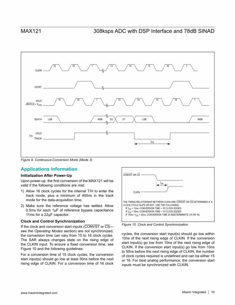
a conversion is initiated (aperture delay). The variation in this delay from one conversion to the next (aperture jitter) is typically 30ps. Figures 7–9 detail the track/hold mode and interface timing for the three different interface modes.
lntemal ReferenceThe MAX121 -5.00V buried-zener reference biases the internal DAC. The reference output is available at the VREF pin and must be bypassed to the AGND pin with a 0.1µF ceramic capacitor in parallel with a 22µF or greater electrolytic capacitor. The electrolytic capacitor’s equiva-lent series resistance (ESR) must be 100mΩ or less to properly compensate the reference output buffer. Sanyo’s organic semiconductor capacitors work well; telephone and FAX numbers are provided below.
Sanyo Video Components (USA) Phone: (619) 661-6835 FAX: (619) 661-1055Sanyo Electric Company, LTD. (Japan) Phone: 0720-70-1005 FAX: 0720-70-1174Sanyo Fisher Vertriebs GmbH (Germany) Phone: 06102-27041, ext. 44 FAX: 06102-27045
Figure 1. MAX121 in the Simplest Operational Mode (Continuous-Conversion Mode)
Figure 2. Equivalent Input Circuit
AIN
VREF CONVST
VSS
VDD CS
CLKIN
MODE
INVFRM
DGND
AGND
TOSERIALPORT
DGND
DGND
10µF
10µF
22µF
0.1µF
0.1µF
0.1µF
AGND
AGND
AGND
DGND
-12V/-15V
+5V
ANALOGINPUT
VDD
CLOCKINPUT
INVCLK SDATA
FSTRT
SCLK
MAX121
DAC
SAR
AIN
VREF
VREF(-5V)
CPACKAGE10pF
CSWITCH2pF
CHOLD7pF
SAMPLINGCOMPARATOR
3kΩ
3kΩ
HOLD
TRACK BUFFER
MAX121 308ksps ADC with DSP Interface and 78dB SINAD
www.maximintegrated.com Maxim Integrated 6

Proper bypassing minimizes reference noise and main-tains a low impedance at high frequencies. The internal-reference output buffer can sink up to 5mA from an external load.An external reference voltage can be used to overdrive the MAX121’s internal reference, if the external reference lies within the range from -5.05V to -5.10V. The external reference must be capable of sinking a minimum of 5mA. The external VREF bypass capacitors are still required.
External ClockThe MAX121 requires a TTL-/CMOS-compatible clock for proper operation. The MAX121 accepts clocks in the frequency range from 0.1MHz to 5.5MHz when operating in mode 1 or mode 2 (see the Operating Modes section). To satisfy the 400ns acquisition-time requirement with 2 clock cycles, the maximum clock frequency is limited to 5MHz when operating in mode 3 (continuous-conversion mode). The minimum clock frequency in all modes is lim-ited to 0.1MHz due to the droop rate of the internal T/H.
Output Data FormatThe conversion result is output as a 16-bit serial data stream, starting with the 14 data bits (MSB first) followed by 2 trailing zeros. The format of the output data is two’s-complement binary. Data is clocked out of the SDATA pin on the rising edge of CLKIN.The output data can be framed using either the FSTRT or the SFRM output. FSTRT (normally low) goes high for 1
clock cycle preceding the MSB. A falling edge on FSTRT indicates that the MSB is available on the SDATA output.The SFRM output (normally high when INVFRM = VDD) goes low coincident with the MSB appearing at the SDATA pin. SFRM returns high 16 clock cycles later. The polarity of SFRM can be inverted by tying the INVFRM input to DGND. A minimum of 18 clock cycles per conver-sion is required to obtain a valid SFRM output.See Figure 3 for the data-access and data-hold timing diagram if several devices share the serial bus. The equivalent load circuits for data-access and data-hold tim-ing are shown in Figures 4 and 5.
Digital InterfaceThe MAX121 serial interface is compatible with SPI and QSPI serial interfaces. In addition, two framing signals (FSTRT and SFRM) are provided to allow the MAX121 to easily interface to most digital-signal processors (DSP) with no external glue logic. The INVCLK input inverts the phase of SCLK relative to CLKIN, and the INVFRM input inverts the phase of the SFRM output. These control signals allow the MAX121 to directly interface to devices with many different serial-interface standards. Specific information for interfacing the MAX121 with SPI, QSPI, and several DSP devices is included in the Applications Information section.
Figure 3. Data-Access + Data-Hold Timing
Figure 4. Load Circuits for Data-Access Time
Figure 5. Load Circuits for Data-Hold Time
Figure 6. Conversion Control Logic
CS
SDATA, SCLK,SFRM + FSTRT HIGH
IMPEDEANCEHIGH
IMPEDEANCEOUTPUTS ENABLED
tDA tDH
SERIALOUTPUTS
SERIALOUTPUTS
3kΩ
3kΩ
CL CL
+5V
DGND
b. HIGH-Z TO VOL (tDA)a. HIGH-Z TO VOH (tDA)
DGND
SERIALOUTPUTS
SERIALOUTPUTS
3kΩ
3kΩ
10pF 10pF
+5V
DGND
b. VOL TO HIGH-Z (tDH)a. VOH TO HIGH-Z (tDH)
DGND
CS
CONVST ADCBUSY
STARTCONVERSION
ENABLEDIGITALOUTPUTS
Q
Q
MAX121 308ksps ADC with DSP Interface and 78dB SINAD
www.maximintegrated.com Maxim Integrated 7

Timing and ControlThe MAX121 has three possible modes of operation, as outlined in the timing diagrams of Figures 7–9 and dis-cussed in the Operating Modes section.In Mode 1, the CONVST input is used to control the start of the conversion. Mode 1 is intended for DSP and other applications where the analog input must be sampled at a precise instant in time.In Mode 2, the CS input controls the start of the conver-sion. This mode is useful when several devices are mul-tiplexed on the same serial data bus, since the MAX121 outputs are placed in a high-impedance state when CS is pulled high.Mode 3 is the continuous-conversion mode. This mode is intended for data logging and similiar applications where the MAX121 is directly linked to memory through a first-in/first-out (FIFO) buffer or a direct memory access (OMA) port.In all three operating modes, the start of conversion is controlled by either the CS or the CONVST input. Both of these inputs must be low for a conversion to take place. Figure 6 shows the logic equivalent for the conversion circuitry. Once the conversion is in progress, it cannot be restarted.
Operating ModesMode 1: CONVST Controls Conversion Starts (MODE = VDD, CS = DGND)Figure 7 shows the timing diagram for mode 1. In this mode, conversion start operations are controlled by the CONVST input.A falling edge on the CONVST input places the T/H into the hold mode and starts a conversion in the successive approximation register (SAR). The FSTRT (normally low) output goes high on the next rising clock edge and remains high for one clock cycle. On the next rising clock edge, FSTRT goes low and the SFRM output goes low (INVFRM = VDD), indicating that the MSB is ready to be latched. SFRM remains high for 16 clock cycles ( 4 data bits plus 2 trailing zeros).The T/H amplifier returns to the track mode when the 14th bit (D0) is clocked out of the SDATA pin. A new conver-sion can be initiated by the CONVST input after the 400ns minimum acquisition time has been satisfied.CS must be low to start a conversion. In applications where the MAX121 interfaces with a dedicated serial port, CS can be hardwired to DGND. To interface the MAX121 to a multiplexed serial bus, CS can be externally driven low to enable conversions, or driven high to place the serial outputs into a high-impedance state.
Figure 7. CONVST Controls Conversion Starts (Mode 1)
CONVST
CLKIN 1
1
13
13
MSB
* THESE CLOCK CYCLES MAY BE OMITTED IF THE SFRM SIGNAL IS NOT NEEDED
D2 LSB
14 15 16* 17*
14 15 16*
SFRM(INVFRM = VDD)
SCLK(INVCRM = VDD)
FSTRT
SDATA
HOLD
TRACKT/H
tAP
tCD
tCW
tAQ
D1
17*
MAX121 308ksps ADC with DSP Interface and 78dB SINAD
www.maximintegrated.com Maxim Integrated 8

Mode 2: CS Controls Conversion Starts (MODE = VDD, CONVST = DGND)Figure 8 shows the timing diagram for mode 2. In mode 2, CS controls the conversion start and enables the serial output pins. Mode 2 is useful in applications where the MAX121 shares the output data bus with other devices. When CS is driven high, the MAX121 is disabled and its serial outputs (SCLK, SDATA, SFRM, and FSTRT) are placed into a high-impedance state.A falling edge on the CS input places the T/H into the hold mode and starts a conversion in the SAR. The FSTRT and SFRM outputs can be used to frame the output data as described in the mode 1 section. CS must remain low for the duration of the conversion. The T/H amplifier returns to the track mode when the 14th bit (D0) is clocked out of the SDATA pin. A new conversion can be initiated by the CS input after the 400ns acquisition time has been satisfied.
Mode 3: Continuous-Conversion Mode (CONVST = CS = MODE = DGND)For applications that do not require precise control of sampling in time, such as data logging, the MAX121 can operate in continuous-conversion mode, directly linked to memory through DMA ports or a FIFO buffer.In this mode, conversions are performed continuously at the rate of one conversion for every 16 clock cycles, which includes 2 clock cycles for the T/H acquisition time. To satisfy the 400ns minimum acquisition-time require-ment within 2 clock cycles, the MAX121 ‘s maximum clock frequency is limited to 5MHz when operating in mode 3.The FSTRT output is used to frame data, as described in the mode 1 section and the mode 3 timing diagram (Figure 9). The SFRM output is meaningless in mode 3, since it will not change state.The MODE input should be hardwired to DGND, since this input must be low when the MAX121 powers up for proper operation of mode 3. To disable conversions, drive CONVST high. To put the serial outputs into a high-impedance state, drive CS high.
Figure 8. CS Controls Conversion Starts (Mode 2)
CS
CLKIN
SFRM(INVFRM = VDC)
HIGHIMPENDANCE
HIGHIMPENDANCE
HIGHIMPENDANCE
HIGHIMPENDANCE
HIGHIMPENDANCE
HIGHIMPENDANCE
HIGHIMPENDANCE
HIGHIMPENDANCE
SCLK(INVCLK = VDC)
FSTRT
SDATA
HOLD
tAP
tCD
1 13 14 15 16* 17*
17*16*1514131
MSB D2 D1 LSB
T/H
* THESE CLOCK CYCLES MAY BE OMITTED IF THE SFRM SIGNAL IS NOT NEEDED
MAX121 308ksps ADC with DSP Interface and 78dB SINAD
www.maximintegrated.com Maxim Integrated 9
Applications InformationInitialization After Power-UpUpon power-up, the first conversion of the MAX121 will be valid if the following conditions are met:1) Allow 16 clock cycles for the internal T/H to enter the
track mode, plus a minimum of 400ns in the track mode for the data-acquisition time.
2) Make sure the reference voltage has settled. Allow 0.5ms for each 1µF of reference bypass capacitance 11ms for a 22µF capacitor.
Clock and Control SynchronizationIf the clock and conversion start inputs (CONVST or CS—see the Operating Modes section) are not synchronized, the conversion time can vary from 15 to 16 clock cycles. The SAR always changes state on the rising edge of the CLKIN input. To ensure a fixed conversion time, see Figure 10 and the following guidelines.For a conversion time of 15 clock cycles, the conversion start input(s) should go low at least 50ns before the next rising edge of CLKIN. For a conversion time of 16 clock
cycles, the conversion start input(s) should go low within 10ns of the next rising edge of CLKIN. If the conversion start input(s) go low from 10ns of the next rising edge of CLKIN. If the conversion start input(s) go low from 10ns to 50ns before the next rising edge of CLKIN, the number of clock cycles required is undefined and can be either 15 or 16. For best analog performance, the conversion start inputs must be synchronized with CLKIN.
Figure 10. Clock and Control Synchronization
Figure 9. Continuous-Conversion Mode (Mode 3)
ICK
CONVST OR CS
CLKIN
THE TIMING RELATIONSHIP BETWEEN CLKIN AND CONVST OR CS DETERMINES IF ACLOCK CYCLE SLIPS OR NOT. USE THE FOLLOWING: IF tCK < 10ns, CONVERSION TIME = 16 CLOCK EDGES IF tCK > 50ns, CONVERSION TIME = 15 CLOCK EDGES IF 10ns < tCK < 50ns, CONVERSION TIME IS INDETERMINATE (15 OR 16)
CLKIN
FSTRT
SDATA
T/H
LSB
15
15 16 1 13 14 15 16 1
tAQ
16 1 13 14 15 16 1
MSB D2 D1 LSB
HOLD
TRACK
SCLK(INVCLK = VCD)
MSB
MAX121 308ksps ADC with DSP Interface and 78dB SINAD
www.maximintegrated.com Maxim Integrated 10

Maximum Clock Rate tor Serial InterfaceThe maximum serial clock rate depends upon the mini-mum setup time required by the receiving processor’s serial data input and the ADC’s maximum clock-to-data delay. The MAX121 allows two fundamentally different methods of clocking data into the processor. In the first clocking method, CLKIN is both the input clock to the MAX121 and the serial clock for the processor. With the second method, CLKIN is the input clock for the MAX121 while SCLK is the serial clock for shifting data into the processor (see Figure 11).The first method would generally be used with simple serial-interface standards (such as SPI) where the pro-cessor does not support asynchronous data transfers. The maximum clock-to-data delay would be tCD + tSC. For this case, calculate the maximum serial clock rate with the following formula:
fCLKIN = (1/2) x 1/(tSU + tCD + tSC)where tSU is the minimum data setup time required at the processor serial data input, tCD is the maximum CLKIN to-SCLK delay of the MAX121, and tSC is the maximum SCLK-to-SDATA delay for the MAX121.The second type of interface is intended for applications where the processor supports asynchronous data trans-fers. The SCLK output of the MAX121 drives the serial clock of the processor, eliminating the tCD term from the above equation and allowing the use of faster clocks. For this case, calculate the maximum serial clock rate with the following formula:
fCLKIN = (1/2) x 1/(tSU + tSC)where the variables are as defined above.
Motorola SPI Serial Interface (CPOL = 0, CPHA = 1)Figure 13 shows the MAX121 and processor interface connections required to support the SPl standard. Figure 12 shows the SPI interface timing diagram. For SPI inter-faces, the processor SS input should be pulled high, to configure the processor as the master. An I/O port from the processor drives the MAX121 CONVST (mode 1) or CS (mode 2) low to control the conversion starts. The SCK output of the processor will drive the CLKIN of the MAX121. The MISO I/O of the processor is driven by the SDATA output of the MAX121.The SPI standard requires that all data transfers occur in blocks of 8 bits, but the MAX121 outputs data in 16-bit blocks. Therefore, two 1-byte read operations are required to receive the full 14 data bits from the MAX121.A conversion is initiated by driving the processor I/O port low. Next, a write operation must be performed by the processor to activate the serial clock and read the first 8 bits of data from the MAX121.The MAX121 output data transitions on the rising edge of the clock. The processor reads data on the falling edge of the clock (CPHA = 1). This provides one half clock cycle to satisfy the minimum setup and hold time requirement of the processor data input. The maximum clock rate for SPI interfaces is 2MHz.The first byte of data read by the processor will consist of a leading zero followed by the 7 MSBs of data. A second write operation should then be initiated to read the second byte of data, which contains the 7 LSBs of conversion data followed by a trailing zero. To minimize errors due to the droop of the MAX121 internal T/H, limit the maximum time delay between the conversion start and the end of the second read operation to no more than 160µs.
Figure 11. Timing Diagram for Serial Data
CLKIN
SCLK(INVCLK = VDD)
SDATA FSTRTSFRM
* tSS CAN BE POSITIVE OR NEGATIVE
tSC*
tCD tCD
MAX121 308ksps ADC with DSP Interface and 78dB SINAD
www.maximintegrated.com Maxim Integrated 11

Motorola QSPI Serial Interlace(CPOL = 0, CPHA = 1)Figure 14 shows the connections required to implement a QSPI interface with the MAX121. The timing diagram for this interface is shown in Figure 15. The QSPI standard is similiar to SPI, with the primary differences as follows:1) QSPI allows arbitrary length data transfers from 8
to 16 bits, so only one read operation is required to receive the 14 bits of output data from the MAX121.
2) QSPI allows clock rates up to 4MHz, compared to 2MHz with SPI.
ADSP2101 Serial InterlaceFigure 16 shows the connections required to interface the MAX121 to Analog Devices’ ADSP2101 DSP. Figure 17 is a plot of the timing diagram. The ADSP2101 has a high-speed serial interface with a minimum serial data setup
time of 10ns (tSCS) and a minimum data-hold time of 10ns (tSCH). This interface permits operation of the MAX121 at its maximum clock rate of 5.5MHz.An output port of the ADSP2101 drives the MAX121 CONVST input low to initiate a conversion. The SFRM output of the MAX121 drives the RFS (Receive Frame Synchronization) input to the DSP low to indicate that the MSB has been shifted out of the MAX121 SDATA pin. On the next falling edge on SCLK, the MSB is shifted into the ADSP2101 serial input. Note that the MAX121 INVFRM input is grounded to provide the proper phase for the SFRM output.The SCLK terminal of the ADSP2101 is configured as an input and is driven by the MAX121 SCLK output to clock data into the DSP. The SFRM output remains low for 16 clock cycles, allowing the 14 data bits to be shifted into the ADSP2101, followed by 2 trailing zeros.
Figure 12. SPI Interface Timing Diagram
Figure 15. QSPI Interface Timing Diagram
Figure 13. SPI Interface Circuit Figure 14. QSPI Interface Circuit
CLKIN
1ST BYTE READ
1 2
MSB D12 D11 D10 D9 D8 D7 D6 D5 D4 D3 D2 D1 D0
3 4 5 6 7 8 1 2 3 4 5 6 7 8
2ND BYTE READ
CONVST
SDATALEADING
ZEROTRAILINGZERO
CLKIN 1 2 3 4 5 6 7 8 9 10 11 12 13 14 15 16
MSB D12 D11 D10 D9 D8 D7 D6 D5 D4 D3 D2 D1 LSB
CONVST
SDATATRAILINGZERO
LEADINGZERO
SS
I/O CONVST
CPOL = 0CPHA = 1
PROCESSOR MAX121
SCK
INVFRM
INVCLKCLKIN
+5V
MISO SDATA CS
DGND
SS
I/O CONVST
CPOL = 0CPHA = 1
PROCESSOR MAX121
SCK
INVFRM
INVCLKCLKIN
+5V
MISO SDATA CS
DGND
MAX121 308ksps ADC with DSP Interface and 78dB SINAD
www.maximintegrated.com Maxim Integrated 12

Figure 17. ADSP2101 Interface Timing Diagram
Figure 18. NEC µP077230 Interlace Circuit
Figure 16. ADSP2101 to MAX121 Interface
CLKIN 1 2 14 15 16 17
LSBMSB
tSCS tSCH
CONVST
SCLK(INVCLK = VCC)
1 2
D12 D1
14 15 16 17
SFRM(INVFRM = GND)
SDATA
SI CONVST
µPD77230 MAX121SCLK SCLK
SIEN
P2
SFRM
CONVST
CLKIN
OSC
CS
INVFRM
INVCLK
DGND
+5V
DMS OR PMS CONVST
ADSP2101 MAX121SCLK SCLK
RFS
DR INVFRMSFRM
SDATA
CLKIN
OSC 0.1MHz ≤ f ≤ 5.5MHz
CS
INVCLK
DGND
+5V
MAX121 308ksps ADC with DSP Interface and 78dB SINAD
www.maximintegrated.com Maxim Integrated 13

NEC µPD77230 Serial InterfaceFigure 18 shows the connections required to interface the MAX121 to NEC’s µPD77230 DSP without external glue logic. The timing diagram is shown in Figure 19. See the Maximum Clock Rate for Serial Interface section to deter-mine the maximum usable clock rate for this interface, substituting tSISS for tSU in the equations. The tHSSI term in the timing diagram is the minimum data-hold time for the µPD77230’s serial data input.An I/O port of the µPD77230 drives the MAX121 CONVST pin low to initiate a conversion. The MAX121 SFRM out-put drives the SIEN (Serial Input Enable) terminal of the DSP low to frame the data. On the next falling edge of SCLK, the MSB is shifted into the SI (Serial Input) pin of the µPD77230. SDATA drives the SI terminal of the DSP. The MSB is followed by the other 13 data bits and two trailing zeros, after which the SFRM output returns high to disable the DSP serial input until the next conversion is initiated.
TMS320 High-Speed Serial InterfaceThe flexibility of the MAX121 permits the implementa-tion of a variety of interfaces with the Texas Instruments’ TMS320 DSP. The TMS320 Simple Serial Interface sec-tion of this data sheet discusses the simplest type of MAX121-to-TMS320 interface, which works with serial clock rates up to 3.2MHz.
This section describes an interface that allows the maximum throughput to be obtained from the MAX121-to-TMS320 system, by operating the MAX121 at its maximum clock. Figure 20 shows the interconnections required to implement this interface. Figure 21 is the tim-ing diagram for this interface.The MAX121 CLKIN is driven by an external clock oscillator. The XFO I/O port of the TMS320 drives the MAX121 CONVST input low to initiate a conversion. CLKR (Receive Clock) of the TMS320 is configured as an input and driven by the MAX121 SCLK output. Data on the MAX121 SDATA output changes state on the rising edge of the clock, while data is latched into the DR input of the TMS320 on the falling edge. This provides one half clock cycle to meet the setup and hold time requirements of the TMS320 DR input. The maximum skew between the MAX121 SCLK and SDATA is ±65ns at +25°C, so one half clock cycle is more than sufficient to guarantee that the setup and hold time requirement is satisfied.The FSTRT output of the MAX121 drives the FSR input of the TMS320 to frame the data. A falling edge on the FSTRT output indicates that the MSB is ready to be latched. On the next falling clock edge, the MSB is latched into the TMS320. For this interface, the TMS320 is config-ured to receive a 16-bit word (RLEN = 01 in the TMS320 serial-port global control register) so the 14 bits of data are clocked into the DSP, followed by two trailing zeros.
Figure 19. NEC µPD77230 Interface Timing Diagram
CLKIN 1 2 14 15 16 17
tSISS tHSS
CONVST
1 2 14 15 16 17SCLK(INVCLK = VDD)
LSBMSB D12 D1
SFRM(INVFRM = GND)
SDATA
MAX121 308ksps ADC with DSP Interface and 78dB SINAD
www.maximintegrated.com Maxim Integrated 14

TMS320 Simple Serial InterfaceFigure 22 shows an application circuit using the simplest interface between the MAX121 and the TMS320. The tim-ing diagram for this circuit is shown in Figure 23. In this circuit, the CLKR port of the TMS320 is configured as a clock output and drives the CLKIN of the MAX121. The MAX121 output changes state on the rising edge of the CLKIN while the data is latched into the DR port of the TMS320 on the falling edge. The XF1 I/O port of the TMS320 drives the MAX121 CONVST input low to initiate a conversion. The FSTRT output of the MAX121 drives the FSR input of the TMS320 to frame the data. A falling edge on the FSTRT output indicates that the MSB is ready to be latched. On the next falling clock edge, the MSB is latched into the TMS320. For this interface, the TMS320 is config-ured to receive a 16-bit word (RLEN = 01 in the TMS320 serial-port global control register) so the 14 bits of data are
clocked into the DSP, followed by two trailing zeros. At TA = +25°C, the clock frequency is limited to approximately 3.2MHz with this interface, due to the CLKIN-to-SDATA maximum delay of 130ns and the 25ns setup and hold time requirement for the TMS320. Figure 24 is a listing of a short program written in the TMS320 assembly language that initiates conversions in the TMS320 and ships the output data back to the host PC. The C language program listed in Figure 25 displays the results of every 30,000th conversion on the PC screen, along with the min and max values for all conver-sions performed during one operating sequence.
Digital Bus/Clock NoiseIf the clock is active when the T/H is sampling the input signal, errors can be caused by coupling from the CLKIN pin to the analog input. If this is a problem, the clock should be disabled for one clock cycle while the T/H is placed into hold mode. In mode 1, the clock should be disabled (CLKIN = DGND) for one cycle while CONVST is pulsed low. In mode 2, the clock should be disabled (CLKIN = DGND) for one clock cycle while CS is driven low. The clock should be reactivated on the first cycle after the conversion is started (CONVST or CS pulsed low).
Layout, Grounding and BypassingFor best system performance, use PCBs with separate analog and digital ground planes. Wire wrap boards are not recommended. The two ground planes should be tied together at the low-impedance power-supply source, as shown in Figure 26.
Figure 21. TMS320 High-Speed Serial-Interface Timing Diagram
Figure 20. TMS320 High-Speed Serial-lnterface Circuit
CLKIN
tSU(FSR) tH(FSR)
CONVST
SCLK
LSBMSB
1 2 14 15
1 2 14 15
D12 D1SDATA
FSTRT
XF CONVST
TMS320 MAX121CLKR SCLK
DR
FSR
SDATA
FSTRT
CLKIN
OSC
CS
INVFRM
INVCLK
DGND
+5V
0.1MHz ≤ F ≤ 5.5MHz
MAX121 308ksps ADC with DSP Interface and 78dB SINAD
www.maximintegrated.com Maxim Integrated 15

The board layout should ensure that digital and analog signal lines are kept separate, as much as possible. Take care not to run analog and digital (especially clock) lines parallel to one another.The high-speed comparator in the ADC is sensitive to high-frequency noise in the VDD and VSS power sup-plies. Bypass these supplies to the analog-ground plane with 0.1µF and 10µF bypass capacitors. Keep capacitor leads at a minimum length for best supply-noise rejection. If the +5V power supply is very noisy, a 5Ω resistor can be connected, as shown in Figure 26, to filter this noise. Figure 27 shows the negative power-supply (VSS) rejec-tion vs. frequency. Figure 28 shows the positive power -supply (VDD) rejection vs. frequency, with and without the optional 5Ω resistor.
Dynamic PerformanceHigh-speed sampling capability and 308kHz throughput make the MAX121 ideal for wideband signal processing. To support these and other related applications, FFT (Fast Fourier Transform) test techniques are used to guarantee the ADC’s dynamic frequency response, distortion, and noise at the rated throughput. Specifically, this involves applying a low-distortion sinewave to the ADC input and recording the digital conversion results for a specified time. The data is then analyzed using an FFT algorithm, which determines its spectral content. Conversion errors are then seen as spectral elements outside of the funda-mental input frequency.ADCs have traditionally been evaluated by specifications such as Zero and Full-Scale Error, Integral Nonlinearity (INL), and Differential Nonlinearity (DNL). Such param-eters are widely accepted for specifying performance with DC and slowly varying signals, but are less useful in signal processing applications where the ADC’s impact on the system transfer function is the main concern. The significance of various DC errors does not translate well to the dynamic case, so different tests are required.
Signal-to-Noise Ratio and Effective Number of BitsThe signal-to-noise plus distortion ratio (SINAD) is the ratio of the fundamental input frequency’s RMS amplitude to the RMS amplitude of all other ADC output signals. The output band is limited to frequencies above DC and below one-half the ADC sample (conversion) rate.The theoretical minimum ADC noise is caused by quanti-zation error and is a direct result of the ADC’s resolution: SINAD = (6.02N + 1.76)dB, where N is the number of bits of resolution. A perfect 14-bit ADC can, therefore, do no better than 86dB. An FFT plot of the output shows the output level in various spectral bands. Figure 29 shows the result of sampling a pure 50kHz sinusoid at a 300kHz rate with the MAX121.By transposing the equation that converts resolution to SINAD, the user can, from the measured SINAD, deter-mine the effective resolution (effective number of bits) that the ADC provides: N = (SINAD - 1.76)/6.02. Figure 30 shows the effective number of bits as a function of the input frequency for the MAX121.
Figure 22. TMS320 Simple Serial-lnterface Circuit
XF CONVST
TMS320 MAX121
CLKR SCLK
DR
FSR
SDATA
FSTRT CS
INVFRM
INVCLK
DGND
+5V
MAX121 308ksps ADC with DSP Interface and 78dB SINAD
www.maximintegrated.com Maxim Integrated 16

Figure 23. TMS320 Simple Serial-Interface Timing Diagram
Figure 24.TMS320 Assembly Language Program to Control Conversions Using the TMS320 Simple Serial Interface
CLKIN
CONVST
1 2 14 15
SDATA
FSTRT
LSBMSB D12 D1
Project : Maxim 121 to TI TMS320C30 Application NoteFile: maximti.asmPurpose: This file contains the code that is loaded onto the TMS320C30 Evaluation Module (EVM). It’s purpose is to collect digitized samples
from the Maxim 121 ADC at a regular rate and ship those values to the PC.Tabstops: 8
$Log : $Edit History:
Date By Description ------ ---- --------------- 09/24/92 KHB Initial Creation
; ; # ; ; ; ; ; ; ; ; ; ; ; ; ; ; ; ; ; ; ; ; ; ; ; ; ; ; ; ; ; ; ; ; ; ; ; ; ; ; ; ; ; ; ; ; ; ; ; ; ; ; ; ; ; ; ; ; ; ; ; ; ; ; ; ; ; ; ; ; ; ; ; ; ; ; ; ; ; ; ; ; ; ; ; ; ; ; ; ; ; ; ; ; ; ; ; ; ; ; ; ; ; ; ; ; ; ; ; ; ; ; ; ; ; ; ; ; ; ; ; ; ; ; ; ; ; ; ; ; ; ; ; ; ; ; ; ; ; ; ; ; ; ; ;; ;; ;; ;; ;; ;; ;; ;; ;; ;; ;; ;; ;; ;; ;; ;; ;; ;; ;; ;; ; ; ; ; ; ; ; ; ; ; ; ; ; ; ; ; ; ; ; ; ; ; ; ; ; ; ; ; ; ; ; ; ; ; ; ; ; ; ; ; ; ; ; ; ; ; ; ; ; ; ; ; ; ; ; ; ; ; ; ; ; ; ; ; ; ; ; ; ; ; ; ; ; ; ; ; ; ; ; ; ; ; ; ; ; ; ; ; ; ; ; ; ; ; ; ; ; ; ; ; ; ; ; ; ; ; ; ; ; ; ; ; ; ; ; ; ; ; ; ; ; ; ; ; ; ; ; ; ; ; ; ; ; ; ; ; ; ; ; ; ; ; # ; ;
MAX121 308ksps ADC with DSP Interface and 78dB SINAD
www.maximintegrated.com Maxim Integrated 17

Figure 24.TMS320 Assembly Language Program to Control Conversions Using the TMS320 Simple Serial Interface (continued)
.global maxim
.global wait_sample
.global wait_loop
.global next_sample
.global IOF_MASK_AMASK
.global IOF_SET_XFI
.global IOF_RESET_XFI
.global CTRL
.global SERGLOB1
.global SERPRTX1
.global SERPRTR1
.global SERTIM1
.global SERTIM1VAL
.global HOST_DATA
IOF_AMASK .word 000000EH ; Preserve XFO settingsIOF_SET_XF1 .word 0000060H ; Set XF1 as output highIOF_RESET_XF1 .word 0000020H ; Set XF1 as output low
CTRL .word 0808000H ; Pointer to peripheral-bus memory map
SERGLOB1 .word 8120280H ; Setup serial 1 global control (80) ; Use internal recieve clock ; FSR active during entire transfer ; 16-bit rcv data length ; FSR active low ; Take rcvr out of resetSERPRTX1 .word 0000000H ; Setup serial 1 xmt port control (82)SERPRTR1 .word 0000111H ; Setup serial 1 rcv port control (83) ; CLKR1 = serial port pin ; DR1 = serial port pin ; FSR1 = serial port pinSERTIM1 .word 00003C0H ; Setup serial 1 timer control (84) ; Start rcv timer, 50% duty cycle, ; internal clk src = 1/2 CLKOUT is ; used to increment rcvr timer.SERTIMIVAL .word 00020000H ; Timer period values RX and TX ; Rcvr timer is high order 16-bits ; (CLKOUT/2)/2 = 1.875Mhz CLKR1 - >MAX121 CLKINHOST_DATA .word 00804000H ; Memory address of host data port
; ; ; ; ; ; ; ; ; ; ; ; ; ; ; ; ; ; ; ; ; ; ; ; ; ; ; ; ; ; ; ; ; ; ; ; ; ; ; ; ; ; ; ; ; ; ; ; ; ; ; ; ; ; ; ; ; ; ; ; ; ; ; ; ; ; ; ; ; ; Publics; ; ; ; ; ; ; ; ; ; ; ; ; ; ; ; ; ; ; ; ; ; ; ; ; ; ; ; ; ; ; ; ; ; ; ; ; ; ; ; ; ; ; ; ; ; ; ; ; ; ; ; ; ; ; ; ; ; ; ; ; ; ; ; ; ; ; ; ; ;
; ; ; ; ; ; ; ; ; ; ; ; ; ; ; ; ; ; ; ; ; ; ; ; ; ; ; ; ; ; ; ; ; ; ; ; ; ; ; ; ; ; ; ; ; ; ; ; ; ; ; ; ; ; ; ; ; ; ; ; ; ; ; ; ; ; ; ; ; ; Data; ; ; ; ; ; ; ; ; ; ; ; ; ; ; ; ; ; ; ; ; ; ; ; ; ; ; ; ; ; ; ; ; ; ; ; ; ; ; ; ; ; ; ; ; ; ; ; ; ; ; ; ; ; ; ; ; ; ; ; ; ; ; ; ; ; ; ; ; ; ; ;
.data
MAX121 308ksps ADC with DSP Interface and 78dB SINAD
www.maximintegrated.com Maxim Integrated 18
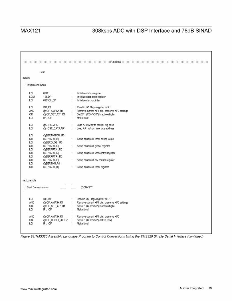
Figure 24.TMS320 Assembly Language Program to Control Conversions Using the TMS320 Simple Serial Interface (continued)
; ; ; ; ; ; ; ; ; ; ; ; ; ; ; ; ; ; ; ; ; ; ; ; ; ; ; ; ; ; ; ; ; ; ; ; ; ; ; ; ; ; ; ; ; ; ; ; ; ; ; ; ; ; ; ; ; ; ; ; ; ; ; ; ; ; ; ; ; ; Functions; ; ; ; ; ; ; ; ; ; ; ; ; ; ; ; ; ; ; ; ; ; ; ; ; ; ; ; ; ; ; ; ; ; ; ; ; ; ; ; ; ; ; ; ; ; ; ; ; ; ; ; ; ; ; ; ; ; ; ; ; ; ; ; ; ; ; ; ; ;
LDI 0,ST ; Initialize status registerLDIU 128,DP ; Initialize data page registerLDI 0985CH,SP ; Initialize stack pointer
LDI IOF,R1 ; Read in I/O Flags register to R1AND @IOF_AMASK,R1 ; Remove current XF1 bits, preserve XF0 settingsOR @IOF_SET_XF1,R1 ; Set XF1 (CONVST*) Inactive (high)LDI R1, IOF ; Make it so!
LDI @CTRL, AR0 ; Load AR0 w/ptr to control reg baseLDI @HOST_DATA,AR1 ; Load AR1 w/host interface address
LDI @SERTIM1VAL,R0STI R0, *+AR0(86) ; Setup serial ch1 timer period valueLDI @SERGLOB1,R0STI R0, *+AR0(80) ; Setup serial ch1 global registerLDI @SERPRTX1,R0STI R0, *+AR0(82) ; Setup serial ch1 xmt control registerLDI @SERPRTR1,R0STI R0, *+AR0(83) ; Setup serial ch1 rcv control registerLDI @SERTIM1,R0STI R0, *+AR0(84) ; Setup serial ch1 timer register
LDI IOF,R1 ; Read in I/O Flags register to R1AND @IOF_AMASK,R1 ; Remove current XF1 bits, preserve XF0 settingsOR @IOF_SET_XF1,R1 ; Set XF1 (CONVST*) Inactive (high)LDI R1, IOF ; Make it so!
AND @IOF_AMASK,R1 ; Remove current XF1 bits, preserve XF0OR @IOF_RESET_XF1,R1 ; Set XF1 (CONVST*) Active (low)LDI R1, IOF ; Make it so!
.text
maxim;; Initialization Code;
next_sample;; Start Conversion -->;
(CONVST*)
MAX121 308ksps ADC with DSP Interface and 78dB SINAD
www.maximintegrated.com Maxim Integrated 19

Figure 24.TMS320 Assembly Language Program to Control Conversions Using the TMS320 Simple Serial Interface (continued)
; ; ; ; ; ; ; ; ; ; ; ; ; ; ; ; ; ; ; ; ; ; ; ; ; ; ; ; ; ; ; ; ; ; ; ; ; ; ; ; ; ; ; ; ; ; ; ; ; ; ; ; ; ; ; ; ; ; ; ; ; ; ; ; ; ; ; ; ; ; ; ; ; ; ; ; ; ; ; ; ; ; ; ; ; ; ; ; ; ; ; ; ; ; ; ; ; ; ; ; ; ; ; ; ; ; ; ; ; ; ; ; ; ; ; ; ; ; ; ; ; ; ; ; ; ; ; ; ; ; ; ; ; ; ; ; ; ; ; ; ; ; ; ; ; ; ; ;
; ; ; ; ; ; ; ; ; ; ; ; ; ; ; ; ; ; ; ; ; ; ; ; ; ; ; ; ; ; ; ; ; ; ; ; ; ; ; ; ; ; ; ; ; ; ; ; ; ; ; ; ; ; ; ; ; ; ; ; ; ; ; ; ; ; ; ; ; ; ; ; ; ; ; ; ; ; ; ; ; ; ; ; ; ; ; ; ; ; ; ; ; ; ; ; ; ; ; ; ; ; ; ; ; ; ; ; ; ; ; ; ; ; ; ; ; ; ; ; ; ; ; ; ; ; ; ; ; ; ; ; ; ; ; ; ; ; ; ; ; ; ; ; ; ; ; ;
LDI *+AR0 (80), R2 ; Read in Serial Ch 1 global registerAND 01H, R2 ; Check for RRDY Active (1) ; RRDY goes active when 16-bits have been rcvdBZ wait_sample ; Keep waiting if not ready
LDI *+AR0 (92), R3 ; Ready, read value from Data Receive registerSTI R3, *+AR1 (0) ; Send out value to host
LDI 100, R0
SUB1 1, R0BNZ wait_loop ; Keep waiting until R0 decremented to zero
BR @next_sample ; Go start next convert
wait_sample;; wait for completion of conversion; MAX121 SFRM Active signals TMS320 FSR1 that data transfer; is ready to start.
;; Arbitrary wait time until start of next convert.;
wait_loop:
.end
MAX121 308ksps ADC with DSP Interface and 78dB SINAD
www.maximintegrated.com Maxim Integrated 20
Figure 25. C Language Program to Log Data from MAX121 Conversions
Project : Maxim 121 to TMS320C30 Application NoteFile: readdata.cPurpose: This file contains a PC based program used to read data from the TMS320C30 Evaluation Module (EVM) and display the
data on the PC screen. This file may be compiled with either the Microsoft C Compiler of Borland C++ Compiler.Tabstops: 4
$Log : $Edit History:
Date By Description ------ ---- --------------- 09/24/92 KHB Initial Creation
#include <stdio.h> /* for printf( ) */#include <conio.h> /* for kbhit( ), getch( ), and inpw */
#define VERSION_STAMP 1
voidmain(void) int x; int value; int quit = 0; int min = 32767; int max = -32768;
printf( “\n”) ; printf( “TMS320 EVM Data Display Program - Version %d\n”, VERSION_STAMP) ;
printf( ”m = reset Max/Min values, ESC to quit\n\n” )`
/ * # * * * * * * * * * * * * * * * * * * * * * * * * * * * * * * * * * * * * * * * * * * * * * * * * * * * * * * * * * * * * * * * * * * * * * * * * * * * * * * * * * * * * * * * * * * * * * * * * * * * * * * * * * * * * * * * * * * * * *
* * * * * * * * * * * * * * * * * * * * * * * * * * * * * * * * * * * * * * * * * * * * * * * * * * * * * * * * * * * * * * * * * * * * * * * * * * * * * * * * * * * * * * * * * * * * * * * * * * * * * * * * * * * * * * * * * * * * * # * /
* ** ** ** ** ** ** ** ** ** ** ** ** ** ** *
MAX121 308ksps ADC with DSP Interface and 78dB SINAD
www.maximintegrated.com Maxim Integrated 21

Figure 25. C Language Program to Log Data from MAX121 Conversions (continued)
while( !quit ) if(kbhit( )) switch ( gletch ( )) case ‘m’ : /* Clear Max/Min Storage Variables */ max = -32768 min = 32767; break; case ‘q’: /* Quit Program */ case 0x1B: quit = 1; break;
for (x=o; x<30000; x++) /* Gather samples as fast as possible and update Max/Min */ /* Only output every 30,000th sample. The 30,000 has no */ /* specific origin other than the display updated at a */ /* comfortable rate. */ value = inpw ( 0x0240+0x0808 ); /* EVM Data Port */ value >>= 2; /* Shift from 16-bit back to 14-bit */
/* Update Max/Min */ If( value > max ) max = value; else if( value < min) main = value; /* Output the latest sample in decimal and hex along with Max/Min */ printf(” %06d %04Xh min:%06d \r”, value, value, min, max);/* Exit */Printf( ‘\n\n” );return;
MAX121 308ksps ADC with DSP Interface and 78dB SINAD
www.maximintegrated.com Maxim Integrated 22

Figure 26. Power-Supply Grounding
Figure 27. VSS Power-Supply Rejection vs. Frequency
Figure 28. VDD Power-Supply Rejection vs. Frequency
Figure 29. MAX121 FFT Plot
FREQUENCY (Hz)
V SS
REJE
CTIO
N (d
B)
100k
40
50
60
3010k 1M
TA = +25°C
FREQUENCY (kHz)
SIGN
AL A
MPLIT
UDE
(dB)
10050
-120
-100
-80
-60
-40
-20
0
0 150
fS = 300kHzIIN = 50kHzTA = +25°CSINAD = 78dB
-15V
-15V-15V
AGND
ANALOGSUPPLY
DIGITALSUPPLY
DIGITALCIRCUITRY
+5V DGND
OPTIONAL5Ω FILTER RESISTOR
DGND
MAX121
+5V
+5VAGND DGND
FREQUENCY (Hz)
V DD
REJE
CTIO
N (d
B)
100k
30
40
50
60
2010k 1M
TA = +25°C
WITH PI FILTER
NO PI FILTER
0.1µF
TOMAX121VDD PIN
VDD+5V
10µF
5Ω PI FILTER
MAX121 308ksps ADC with DSP Interface and 78dB SINAD
www.maximintegrated.com Maxim Integrated 23
Total Harmonic DistortionIf a pure sine wave is sampled by an ADC at greater than the Nyquist frequency, the nonlinearities in the ADC’s transfer function create harmonics of the input frequency present in the sampled output data.Total Harmonic Distortion (THD) is the ratio of the RMS sum of all the harmonics (in the frequency band above DC and below one-half the sample rate, but not including the DC component) to the RMS amplitude of the fundamental frequency. This is expressed as follows:
2 2 2 22 3 4 N
1
V + V + VTHD =
+ V 20 log
V
where V1 is the fundamental RMS amplitude, and V2 through VN are the amplitudes of the 2nd through Nth harmonics. The THD specification in the Electrical Characteristics includes the 2nd through 5th harmonics.
Spurious-Free Dynamic RangeSpurious-free dynamic range is the ratio of the fundamen-tal RMS amplitude to the amplitude of the next largest spectral component (in the frequency band above DC and below one-half the sample rate). Usually the next largest spectral component occurs at some harmonic of the input frequency. However, if the ADC is exceptionally linear, it may occur only at a random peak in the ADC’s noise floor.
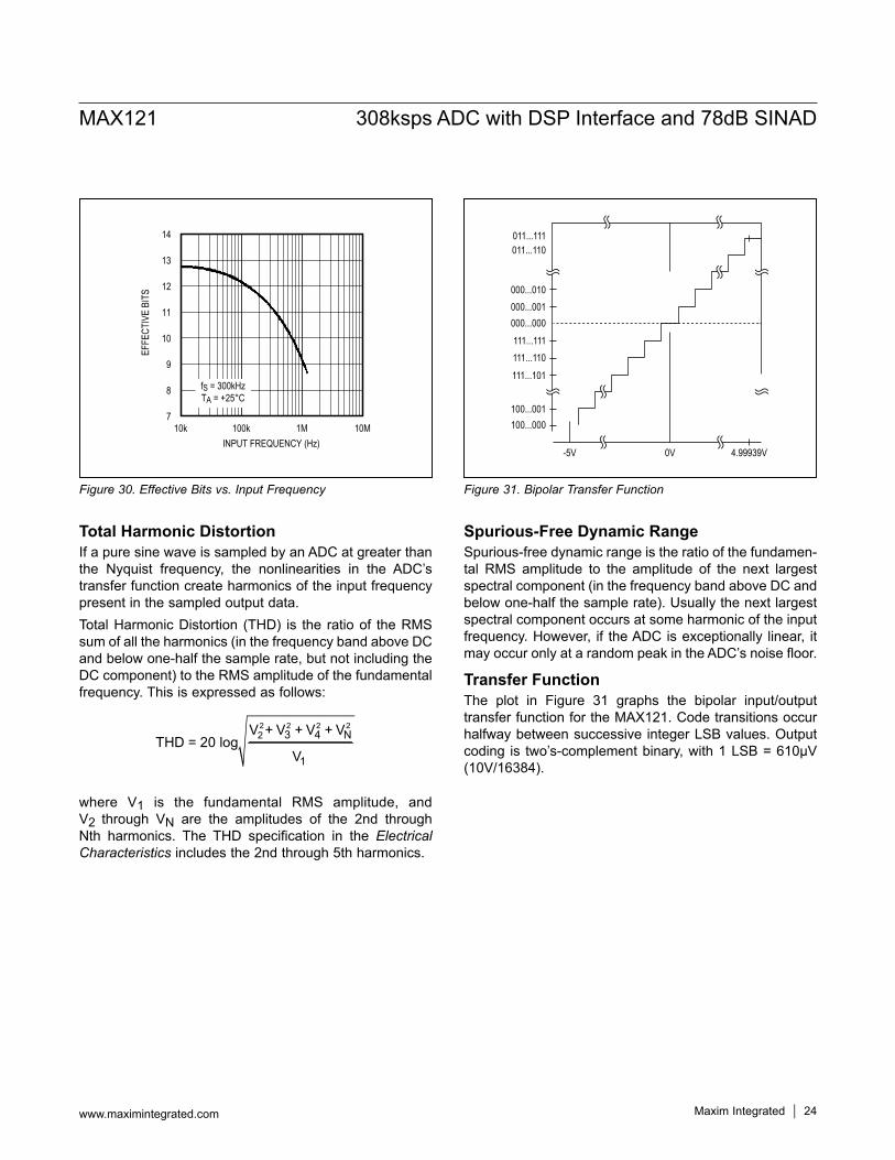
Transfer FunctionThe plot in Figure 31 graphs the bipolar input/output transfer function for the MAX121. Code transitions occur halfway between successive integer LSB values. Output coding is two’s-complement binary, with 1 LSB = 610µV (10V/16384).
Figure 30. Effective Bits vs. Input Frequency Figure 31. Bipolar Transfer Function
INPUT FREQUENCY (Hz)
EFFE
CTIV
E BI
TS
1M100k
8
9
10
11
12
13
14
710k 10M
fS = 300kHzTA = +25°C
0V-5V
100...001
111...101111...110111...111
000...000000...001000...010
011...110011...111
100...000
4.99939V
MAX121 308ksps ADC with DSP Interface and 78dB SINAD
www.maximintegrated.com Maxim Integrated 24

+Denotes a lead(Pb)-free/RoHS-compliant package.*20-pin SSOP is 50% smaller than 16-pin SO.
PART TEMP RANGE PIN-PACKAGEMAX121CPE+ 0°C to +70°C 16 PDIP
MAX121CWE+ 0°C to +70°C 16 Wide SO
MAX121CAP+ 0°C to +70°C 20 SSOP*
MAX121EPE+ -40°C to +85°C 16 PDIP
MAX121EWE+ -40°C to +85°C 16 Wide SO
MAX121EAP+ -40°C to +85°C 20 SSOP*
MAX121EVKIT-DIP 0°C to +70°C Through-Hole
PACKAGE TYPE
PACKAGE CODE OUTLINE NO. LAND
PATTERN NO.
16 PDIP P16+3 21-0043 —
16 Wide SO W16+2 21-0042 90-0107 20 SSOP A20+1 21-0056 90-0094
MAX121 308ksps ADC with DSP Interface and 78dB SINAD
www.maximintegrated.com Maxim Integrated 25
Package InformationFor the latest package outline information and land patterns (footprints), go to www.maximintegrated.com/packages. Note that a “+”, “#”, or “-” in the package code indicates RoHS status only. Package drawings may show a different suffix character, but the drawing pertains to the package regardless of RoHS status.
Chip InformationPROCESS: BiCMOS
Ordering Information

REVISIONNUMBER
REVISIONDATE DESCRIPTION PAGES
CHANGED
0 1/93 Initial release —
3 1/12 Remove military grade and update Ordering Information 1–4, 24
Maxim Integrated cannot assume responsibility for use of any circuitry other than circuitry entirely embodied in a Maxim Integrated product. No circuit patent licenses are implied. Maxim Integrated reserves the right to change the circuitry and specifications without notice at any time. The parametric values (min and max limits) shown in the Electrical Characteristics table are guaranteed. Other parametric values quoted in this data sheet are provided for guidance.
Maxim Integrated and the Maxim Integrated logo are trademarks of Maxim Integrated Products, Inc.
MAX121 308ksps ADC with DSP Interface and 78dB SINAD
© 2012 Maxim Integrated Products, Inc. 26
Revision History
For pricing, delivery, and ordering information, please contact Maxim Direct at 1-888-629-4642, or visit Maxim Integrated’s website at www.maximintegrated.com.