materials science: from research to technologycms.iopscience.iop.org/.../materials-science.pdf ·...
TRANSCRIPT

Materials science: from research to technologyiopscience.org/materials-science

Advanced Material Testing
NEW – Vacuum-tight Thermo-Microbalance TG 209 F1 Libra®
The ability to begin measuring immediately upon start-up increases productivityNo baseline determination needs to be carried out – BeFlat® function automatically compensates for any external factors
Faster resultsHeating rates of up to 200 K/min due to the new high-performance ceramics used in the micro furnace
Long LifespanLifespan is many times longer due to the new furnace concept – even when investigating substances containing corrosive components
NETZSCH-Gerätebau GmbH
Wittelsbacherstraße 42 95100 SelbGermanyTel.: +49 9287 881-0 Fax: +49 9287 881 [email protected]/tg209f1
Faster, Easier and More
Comprehensive Characterization
of Materials

3
iopscience.org/mater ials - sc ience
Materials science: from research to technology
Contents
Materials for fuel-cell membranes p7
Small features in epitaxial graphene p15
Welcome 5
Materials for energy technologies 7● Nanowires promise solar success ● New views inside a fuel-cell membrane ● Nanostructures for photovoltaics ● Reeling in cheap plastic solar film ● New light dawns on solar energy ● Single-layer graphene delivers photocurrent ● Bar-milled graphite for better batteries
Soft materials and biomaterials 11● Bioprinting builds tissue structures ● Injectable hydrogels deliver biological success ● The unbearable heaviness of colloids ● Spider webs offer engineering lessons ● Nanofibres mimic natural bone ● Nanoparticles deliver drugs into brain ● Simulations produce new insight into bacterial flow ● Biomedical engineering
Functional materials and nanomaterials 15● Graphene growth hits the big time ● Nanowires speed up light detectors ● Stepped substrate generates ordered nanostripes ● Corrosion carves out 3D nanostructures ● Applications beckon for graphene spintronics ● Brighter future for carbon dots ● Nanofibres sense the future ● Metamaterials
Structural and advanced materials 19● High-grade steels reach new heights ● Topological insulators: fabricating devices without doping ● Knee device hints at end for batteries ● Robot jellyfish fuelled by hydrogen ● Smart adhesives detect aircraft failure ● New horizons in adaptive and active materials ● Curtains for noise
Synthesis, characterization and modelling methods 23● Simulations probe polycrystals ● Supercomputers power nanomaterial design ● Mapping out crystal structure ● Lissajous curves speed SPM imaging ● Graphyne: the next wonder material? ● Taking control of self-assembly ● Nanomagnets built one atom at a time
IOP materials science journals 26● Biofabrication ● Biomedical Materials ● Computational Science & Discovery ● Journal of Physics: Condensed Matter ● Journal of Physics D: Applied Physics ● Modelling and Simulation in Materials Science and Engineering ● Nanotechnology ● Science and Technology of Advanced Materials ● Semiconductor Science and Technology ● Smart Materials and Structures
Other IOP journals covering the scope of materials science 28 IOP Publishing supporting the materials science community 29
Editor Susan CurtisProduction Editor Alison GardinerMarketing Manager Claire WebberMarketing Executive Zoe AndersonAdvertisement Sales Chris ThomasAdvertisement Production Mark TrimnellDiagram Artist Alison ToveyArt Director Andrew Giaquinto
Copyright © 2012 by IOP Publishing Ltd and individual contributors. All rights reserved
Temple Circus, Temple Way,Bristol BS1 6HG, UKTel +44 (0)117 929 7481E-mail [email protected] ioppublishing.org
Materials science: from research to technology
Research benefits high-grade steels p19

www.goodfellow.com
Metalsand materialsfor research
SMALLQUANTITIES
FASTDELIVERY
70 000PRODUCTS
CUSTOMFABRICATION
GoodfellowCambridge LimitedErmine Business ParkHuntingdonPE29 6WR UKTel: 0800 731 4653 or+44 1480 424 800Fax: 0800 328 7689 or+44 1480 424 [email protected]
ON-LINE CATALOGUE
Werkstoffe_193x262_uk:Mise en page 1 22/10/12 12:33 Page 1
Untitled-7 1 22/10/2012 13:10

iopscience.org/mater ials - sc ience
5
Materials science: from research to technology
Welcome
Materials research has always acted as a crucible for scientific discovery. The creative mash-up between biology, chemistry and physics has produced a steady stream of game-changing innovations, ranging from such household names as Teflon® and Velcro® to more recent technological marvels like graphene and carbon nanotubes. Today’s research into exotic materials and novel structures promises to have just as broad an impact in areas as diverse as healthcare, next-generation electronics, and sustainable energy technologies.
This special collection of content from IOP Publishing offers a snapshot of that scientific crucible in action. You’ll find articles from our broad portfolio of journals, magazines and websites that show how scientists are using all of their ingenuity to solve some of the biggest problems facing society today. High-performance materials for solar photovoltaics and energy storage, better ways to deliver drugs and fabricate artificial implants, and safer and stronger construction materials are just a few of the subjects covered in the collection.
If you like what you read, there’s much more to explore in our online collection at iopscience.org/materials-science. The collection highlights research articles that we feel are making a significant contribution to this fast-moving field – whether by exploring the behaviour of novel materials, conceiving new formulations or structures, or finding clever ways to fabricate materials for real-world applications.
And if you’re inspired by all of this fantastic research, then why not consider submitting your next paper to an IOP Publishing journal? You’ll find a full run-down of relevant journals on pp26–28, followed by some top tips to help you submit your work to IOP Publishing.
We hope that you enjoy this special collection, and we hope to have the opportunity to work with you soon.
Susan CurtisManaging editor, IOP [email protected]
Cover image: A computer model reveals the interference patterns formed by quantum waves in a topological insulator, showing how numerical and quantum models can be used together to predict the properties of new materials. Credit: A Yazdani/SPL.

April 1–5, San Francisco, CA
SAVE THE DATE
MATERIALS RESEARCH SOCIETY Advancing materials. Improving the quality of life.
ENERGY NANOMATERIALS ELECTRONICS/PHOTONICS BIOMATERIALS GENERAL
Meeting Registration Opens Late January 2013
2013 MRS SPRING MEETING CHAIRS
Mark L. Brongersma Stanford University Vladimir Matias iBeam Materials, Inc. Rachel Segalman University of California, Berkeley Lonnie D. Shea Northwestern University Heiji Watanabe Osaka University
www.mrs.org/spring2013
Tel: +44 (0)1256 467055, Fax: +44 (0)1256 842929, Email: [email protected], www.testbourne.com
Testbourne LtdProducts for Industry, Research & Development
Unit 2, Hatch Industrial Park, Greywell Road, Hatch, Basingstoke, Hampshire, RG24 7NG, England
Testbourne Ltd has been supplying high purity metals, alloys & compounds to industries such as photovoltaics, glass coatings, data storage, thin-films, electronics, electro-optics and research establishments for over 30 years. You will find an extensive selection of materials available in fabricated forms including sputtering targets, evaporation materials, powders, wires, rods & sheets.
We can also accommodate any custom requirements you may have.
Visit us at: www.testbourne.com

7
iopscience.org/mater ials - sc ience
Materials science: from research to technology
Membrane dynamics Measuring proton conductivity is crucial for developing improved fuel cells.
Nafion membranes are widely used as electrolytes in polymer electrolyte fuel cells, and the proton conductivity of Nafion is one of the key parameters for achieving high-power densities. Measuring the proton conductivity has traditionally relied on impedance spectroscopy, which achieves a mac-roscopic resolution of around 1 cm2, but the mechanisms that influence Nafion’s proton conductivity operate on a much smaller scale.
In an article for Journal of Physics: Condensed Matter, a team of German scientists have shown that electro-chemical atomic force microscopy (EC-AFM), which uses a conductive tip as a nano-sized electrode that scans across the membrane surface,
can measure proton conductivity on a scale of 100 nm2, some 10 orders of magnitude better than for imped-ance spectroscopy.
EC-AFM can also reveal infor-mation about the dynamics within the Nafion polymer, as well as its structure. This is important because a polymer like Nafion, which has water-repelling backbones and polar side groups, forms hydrophobic and hydrophilic domains. The hydro-philic domains connect by perco-lation as the water content of the polymer increases, creating a net-work of water-containing channels that controls the proton conductivity of the fuel cell membrane.
The new results confirm the model
of a network of conducting channels, but they also reveal pronounced in- homogeneities. New pores open up, which, together with existing pores, enhance the conductivity as the water content of the membrane increases.
Changes in the proton conductiv-ity when a voltage is applied suggest that the distribution of water fluctu-ates over time, even when the system is in equilibrium. If enough current is drawn, the conductivity reaches a critical value and breaks down due to local water depletion by osmotic drag. The researchers believe that the results will be important for opti-mizing water management and mem-brane conductivity in fuel cells.J. Phys.: Condens. Matter 23 234109
New views inside a fuel-cell membraneJournal of Physics: Condensed Matter
Sun seeker New designs based on InGaN/GaN nanowires could boost conversion efficiencies.
Indium gallium nitride (InGaN) semiconductors are often described as potential next-generation photo-voltaic materials. The energy absorp-tion of the alloy can be tuned across the entire solar spectrum by vary-ing its composition, which in theory should lead to devices with higher conversion efficiencies.
Unfortunately, there are some fabrication issues to contend with. InGaN layers are grown on thin films of GaN, and the mismatch between their atomic lattices induces struc-tural strain between the layers, limit-ing the amount of indium that can be included in the InGaN layer. Under these conditions InGaN is only able to absorb at the highest energies of the solar spectrum and the resulting solar cells only have low power-con-version efficiencies.
To overcome these strain limita-tions, a team of scientists at Sandia National Laboratories in the US has grown InGaN-based shell layers on a GaN nanowire array, rather than
on a flat thin film. Reporting their results in the journal Nanotechnol-ogy, the researchers say that the small surface area of the nanowires allows the shell layer to partially relax along each wire to accommodate the increased indium content.
The team used several unique
techniques to create this novel solar cell. First, the nanowire array was produced in a top-down fabrication process, which involved masking an n-type GaN layer with colloidal silica and then dry and wet etching. Next, shell layers were formed on the GaN nanowire template via metal organic chemical vapour deposition, creating a InGaN/GaN multiple quantum well structure with indium percentages of 33%. Last, a p-type In0.02Ga0.98N layer was grown. Here, the close proximity of the nanowires allowed the material to coalescence, which produced a canopy over the top of the structure and facilitated simple planar processing.
This approach enabled the team to lower the energy band gap of the solar cells from 2.4 to 2.1 eV, the low-est of any III-nitride solar cell to date. In future work, the scientists plan to refine the nanowire templates, which should lead to higher efficiencies and even lower energies. Nanotechnology 23 194007
Nanowires promise solar success
Materials for energy technologies

iopscience.org/mater ials - sc ienceMaterials for energy technologiesMaterials science: from research to technology
8
Solar for rural areas One of the small solar panels provided by Eight19 powers a house in Nimule, South Sudan.
A UK-based start-up is develop-ing printable, thin-film plastic solar cells aimed at providing affordable electricity to homes that have no grid connection, such as those in rural Africa. The flexible device’s photo-active layer will contain two organic semiconductor materials positioned between metallic electrodes, all sandwiched by plastic substrates. The firm plans to start manufactur-ing the sheets by 2013.
Eight19, a Cambridge University spin-off firm, is named after the 8 min, 19 s it takes sunlight to reach the Earth. Its founders believe that their lightweight films will slash the cost of transporting and installing solar panels compared with con-ventional solar panels or cells. This should make it more affordable for farmers and villagers in remote areas, who can fix the sheets to their roofs to power their homes.
The design involves a photoactive layer of two organic semiconductor materials: a polymer for the “donor” and a fullerene for the “acceptor”. Sunlight creates excitons – bound pairs of electrons and holes – that dif-fuse into the interface where the poly-mer and fullerene meet, known as an artificial “heterojunction”. Here, the pairs split apart, with the electrons moving to the film’s metallic cathode layer and the holes to the anode.
Eight19 plans to deploy a transpar-ent metal for the anode, so that sun-light is not prevented from hitting the photoactive layer. The cathode could be a semi-transparent conductor or an opaque metal, which would cause the light to bounce back onto the
Physics World
Reeling in cheap plastic solar film
photoactive layer. The outer protective layers will be
formed with polyethylene terephtha-late (PET) so that the films remain lightweight and flexible. The plan is to deposit the electrode and photo-active layers onto a PET substrate using reel-to-reel printing. Although PET does not last as long as glass – a module will last around five years, compared with 25 years for conven-tional panels – tougher versions can be made by adding extra PET layers.
The company claims that a small, 2.5 MW sheet should provide enough electricity for rudimentary LED lighting and mobile-phone charg-ing. Larger sheets will power media devices and appliances.
Eight19 currently provides areas in Kenya, South Sudan, Malawi and Zambia with an innovative service – it sells $10 kits containing small, 2.5 W conventional solar panels, two LED lamps and a rechargeable lithium-ion battery. For $1 per week, kit owners buy a scratch card and text the card’s number, receiving a code that allows unlimited use of the panel.
Nanostructured mater ials are expected to drive the development of new photovoltaic technologies that allow more solar energy to be con-verted into electrical power.
To support research in this rapidly evolving field, Journal of Physics D: Applied Physics is publishing a special issue on Nanostructured Photovolta-ics in December 2012.
Guest edited by Lan Fu, Hoe Tan and Chennupati Jagadish of the Australian National University, the articles in the special issue will cover different design approaches, includ-ing quantum-dot structures, organic solar cel ls , and dye-sensitized devices. Light-trapping techniques to improve conversion efficiencies will also be discussed.
Nanostructures for photovoltaics
Journal of Physics D: Applied Physics
Light trapping Nanoshells of silicon can improve the absorption of solar radiation.
Journal of Physics DApplied Physics
iopscience.org/jphysd
ISSN 0022-3727
Journal of Physics DApplied Physics
Volume 45 Number 40 10 October 2012
Topical reviewQuadrupole mass spectrometry of reactive plasmasJ Benedikt, A Hecimovic, D Ellerweg and A von Keudell
Stay up to date with the latest special issues from Journal of Physics D
iopscience.org/jphysd/specialissuesImpact Factor
As listed in 2011 Journal Citation reports (Thomson Reuters 2012)®
2.544
SOME ARTICLES IN THIS ISSUE
Sputter-grown Si quantum dot nanostructures for tandem solar cellsGavin Conibeer et al
Self-organized InGaAs/GaAs quantum dot arrays for use in high-efficiency intermediate-band solar cellsYoshitaka Okada et al
Exploration of nano-imprinted organic photovoltaic: influence of nanostructure in the deviceRene Lopez et al
A novel carbon-PEDOT composite counter electrode for monolithic dye sensitised solar cellsYibing Cheng et al

9
LabTalkBall-milled graphite for better batteriesLithium-ion batteries are one of the most popular energy-storage systems for portable electronics, since they offer one of the best energy densities, no memory effect, and suffer only a slow loss of charge when not in use. One key focus of current research is to enhance the energy density of commercial systems by introducing enhanced materials for the negative electrode.
Graphitic carbon has been widely studied because it can accommodate lithium atoms rapidly, reversibly and without generating much mechanical stress. Pristine graphitic carbon can accommodate up to one lithium atom per six carbon atoms, which yields a charge storage capacity of 372 mA h g–1.
Experiments have shown that carbon nanostructures can store 2–3 times more lithium than bulk graphitic carbon, but these approaches remain too expensive for large-scale industrial applications. Ball-milled carbons offer a more practical alternative, but the increased lithium storage in these materials has puzzled scientists because it has been found to fluctuate with the milling time.
X-rays reveal graphitic structureWriting in Journal of Physics: Condensed Matter, a US collaboration between scientists at General Motors, the Advanced Photon Source at Argonne National Laboratory and Central Michigan University reports on the use of high-energy X-ray diffraction (XRD) to investigate how lithium intercalates in ball-milled carbons.
For short milling times they find that the graphitic planes break into smaller pieces and remain quite flat. This allows the lithium atoms to be accommodated within the layers, which increases the storage capacity to about 900 mA h g–1. For longer milling times, the graphitic layers become buckled and fuse together, making it increasingly difficult for lithium to intercalate between them and so reducing the overall storage capacity.
The researchers conclude that technology routes that produce fine graphitic platelets should be explored to maximize the lithium storage capacity. They also recommend the use of total XRD to provide precise structural information on the complex materials that are now being studied for energy-storage applications.J. Phys.: Condens. Matter 23 435003
Materials for energy technologiesiopscience.org/mater ials - sc ience
Materials science: from research to technology
Semiconductor Science and Technology
New light dawns on solar energyA special collection of articles in Semiconductor Science and Tech-nology highlights recent research to improve the efficiency and reduce the cost of photovoltaics and solar cells. Since the first practical pho-tovoltaic cell was developed at Bell Laboratories in 1954, research inter-est has intensified as solar power has emerged as a practical and sustain-able source of clean energy.
The articles cover a range of
challenges facing the research community, including the design, characterization and use of photo-voltaic devices in real-life applica-tions. Novel design approaches are also discussed, including devices made from quantum dots, nanowires and thin films. Material systems cov-ered by the articles include silicon, cadmium telluride and compound semiconductors as well as a range of organic materials.
Using a simple air-assisted fabrica-tion process, researchers from the Small Systems Laboratory at the University of Louisville, US, have demonstrated large photocurrents in single-layer graphene assemblies when they are illuminated with near-infrared light. The group, reporting their work in Nanotechnology, say that the results could pave the way for low-cost solar cells, as well as graphene-based photodetectors and infrared bolometers.
In the study, photocurrents in excess of 1800% of dark current were obtained when the graphene struc-tures were irradiated with 335 mW of near-infrared light. The photo-current was also found to depend on position, increasing when the positive electrode was illuminated, decreas-ing when the negative electrode was illuminated, and showing a negligi-ble response when the area between the electrodes was illuminated.
According to the team, such large responses result from built-in electric fields and optically generated temper-ature gradients. These low-density thin films not only exhibit interesting morphology, but also demonstrate classic Haynes-Shockley characteris-tics of drift and diffusion.
The single-layer graphene films are fabricated using a straight- forward air-assisted deposition pro-cess, which does not require litho-graphic patterning, and produces devices with reliable and repeatable photocurrent responses. The sim-ple shadow/spray masking for gold/ graphene deposition could be of inter-est in astronomy, telecommunication and imaging applications, while the researchers believe that demonstrat-ing Haynes-Shockley experiments in graphene thin films could offer a valuable educational tool for young scientists and engineers.Nanotechnology 23 265203
Single-layer graphene delivers photocurrentNanotechnology
Spray coated A simple fabrication technique could lead to low-cost solar cells.
SOME ARTICLES IN THIS COLLECTION
Photoconductivity peculiarities in InGaAs quantum wire heterostructures: anisotropy and high photoresponsivity at room temperatureS V Kondratenko, O V Vakulenko, Vas P Kunets, Yu I Mazur, V G Dorogan, M E Ware and G J Salamo Semicond. Sci. Technol. 27 105024
Flexible organic/inorganic hybrid solar cells based on conjugated polymer and ZnO nanorod arrayFei Tong, Kyusang Kim, Daniel Martinez, Resham Thapa, Ayayi Ahyi, John Williams, Dong-Joo Kim, Sungkoo Lee, Eunhee Lim, Kyeong K Lee and Minseo Park Semicond. Sci. Technol. 27 105005
Atomic layer deposition for photovoltaics: applications and prospects for solar cell manufacturingJ A van Delft, D Garcia-Alonso and W M M KesselsSemicond. Sci. Technol. 27 074002

METALS & ALLOYS for Research / Development & IndustrySmall Quantities • Competitive Prices • Fast Shipment
57-70
*
89-102
**
*Lanthanoids
**Actinoids
Periodic Table of the Elements
1
2
3 4 5 6 7 8 9 10 11 12
13 14 15 16 17
18
1.00790.090-252.87
Hydrogen
H1
6.9410.54180.5
Lithium
Li39.01221.851287
Beryllium
Be4
22.9900.9797.7
Sodium
Na1124.3051.74650
Magnesium
Mg12
39.0980.8663.4
Potassium
K1940.0781.55842
Calcium
Ca20
85.4681.5339.3
Rubidium
Rb3787.622.63777
Strontium
Sr38
132.911.8828.4
Caesium
Cs55137.333.51727
Barium
Ba56
[223]––
Francium
Fr87[226]5.0700
Radium
Ra88
138.916.146920
Lanthanum
La57140.126.689795
Cerium
Ce58140.916.64935
Praseodymium
Pr59144.246.801024
Neodymium
Nd60[145]7.2641100
Promethium
Pm61150.367.3531072
Samarium
Sm62151.965.244826
Europium
Eu63157.257.9011312
Gadolinium
Gd64158.938.2191356
Terbium
Tb65162.508.5511407
Dysprosium
Dy66164.938.7951461
Holmium
Ho67167.269.0661497
Erbium
Er68168.939.3211545
Thulium
Tm69173.046.57824
Ytterbium
Yb70
[227]10.071050
Actinium
Ac89232.0411.721842
Thorium
Th90231.0415.371568
Protactinium
Pa91238.0319.051132
Uranium
U92[237]20.45637
Neptunium
Np93[244]19.816639
Plutonium
Pu94[243]–
1176
Americium
Am95[247]13.511340
Curium
Cm96[247]14.78986
Berkelium
Bk97[251]15.1900
Californium
Cf98[252]–860
Einsteinium
Es99[257]–
1527
Fermium
Fm100[258]–827
Mendelevium
Md101[259]–827
Nobelium
No102
44.9562.991541
Scandium
Sc2147.8674.511668
Titanium
Ti2250.9426.111910
Vanadium
V2351.9967.141907
Chromium
Cr2454.9387.471246
Manganese
Mn2555.8457.871538
Iron
Fe2658.9338.901495
Cobalt
Co2758.6938.911455
Nickel
Ni2863.5468.921084.6
Copper
Cu2965.397.14419.5
Zinc
Zn3069.7235.9029.8
Gallium
Ga3172.645.32938.3
Germanium
Ge3274.9225.73816.9
Arsenic
As3378.964.82221
Selenium
Se3479.9043.12-7.3
Bromine
Br3583.803.733-153.22
Krypton
Kr36
10.8112.462076
Boron
B512.0112.273900
Carbon
C614.0071.251-195.79
Nitrogen
N715.9991.429-182.95
Oxygen
O818.9981.696-188.12
Fluorine
F920.1800.900-246.08
Neon
Ne10
26.9822.70660.3
Aluminium
Al1328.0862.331414
Silicon
Si1430.9741.8244.2
Phosphorus
P1532.0651.96115.2
Sulphur
S1635.4533.214-34.04
Chlorine
Cl1739.9481.784-185.85
Argon
Ar18
4.00260.177-268.93
Helium
He2
88.9064.471526
Yttrium
Y3991.2246.511855
Zirconium
Zr4092.9068.572477
Niobium
Nb4195.9410.282623
Molybdenum
Mo42[98]11.52157
Technetium
Tc43101.0712.372334
Ruthenium
Ru44102.9112.451964
Rhodium
Rh45106.4212.021554.9
Palladium
Pd46107.8710.49961.8
Silver
Ag47112.418.65321.1
Cadmium
Cd48114.827.31156.6
Indium
In49118.717.31231.9
Tin
Sn50121.766.70630.6
Antimony
Sb51127.606.24449.5
Tellurium
Te52126.904.94113.7
Iodine
I53131.295.887-108.05
Xenon
Xe54
174.979.841652
Lutetium
Lu71178.4913.312233
Hafnium
Hf72180.9516.653017
Tantalum
Ta73183.8419.253422
Tungsten
W74186.2121.023186
Rhenium
Re75190.2322.613033
Osmium
Os76192.2222.652466
Iridium
Ir77195.0821.091768.3
Platinum
Pt78196.9719.301064.2
Gold
Au79200.5913.55-38.83
Mercury
Hg80204.3811.85304
Thallium
Tl81207.211.34327.5
Lead
Pb82208.989.78271.3
Bismuth
Bi83[209]9.20254
Polonium
Po84[210]–302
Astatine
At85[222]9.73-61.85
Radon
Rn86
[262]–
1627
Lawrencium
Lr103[265]––
Rutherfordiu
m104
[268]––
Dubnium
Db105[271]––
Seaborgium
Sg106[272]––
Bohrium
Bh107[270]––
Hassium
Hs108[276]––
Meitnerium
Mt109[281]––
Darmstadtium
Ds110[280]––
Roentgenium
Rg111[285]––
Copernicium
Cn112[289]––
Ununquadium
Uuq114
Solids�& Liquids (g/cm3)�Gases(g/l)
€
Melting�point�(Solids�&�Liquids)�•�Boiling�point�(Gases)
€
Standard Catalogue Items
Element Name
SymbolAtomic�weight
DensityM.pt./B.pt.(˚C)
AtomicNo.
advent-rm.com� � � � � � � � �
ADVENT
[284]––
Ununtrium
Uut113[288]––
Ununpentium
Uup115[293]––
Ununhexium
Uuh116
Tel + 44 1865 884440Fax + 44 1865 [email protected]
RESEARCH MATERIALS
[–]––
Ununseptium
Uus117[294]––
Ununoctium
Uuo118
85595�P�T�A5�2010��14/07/2010��14:14��Page�1
Advent�Research�Materials�Ltd�•�Oxford�•�England�OX29�4JA
METALS & ALLOYS for Research / Development & IndustrySmall Quantities • Competitive Prices • Fast Shipment
57-70
*
89-102
**
*Lanthanoids
**Actinoids
Periodic Table of the Elements
1
2
3 4 5 6 7 8 9 10 11 12
13 14 15 16 17
18
1.00790.090
-252.87
Hydrogen
H1
6.9410.54180.5
Lithium
Li39.01221.851287
Beryllium
Be4
22.9900.9797.7
Sodium
Na1124.3051.74650
Magnesium
Mg12
39.0980.8663.4
Potassium
K1940.0781.55842
Calcium
Ca20
85.4681.5339.3
Rubidium
Rb3787.622.63777
Strontium
Sr38
132.911.8828.4
Caesium
Cs55137.333.51727
Barium
Ba56
[223]––
Francium
Fr87[226]5.0700
Radium
Ra88
138.916.146920
Lanthanum
La57140.126.689795
Cerium
Ce58140.916.64935
Praseodymium
Pr59144.246.801024
Neodymium
Nd60[145]7.2641100
Promethium
Pm61150.367.3531072
Samarium
Sm62151.965.244826
Europium
Eu63157.257.9011312
Gadolinium
Gd64158.938.2191356
Terbium
Tb65162.508.5511407
Dysprosium
Dy66164.938.7951461
Holmium
Ho67167.269.0661497
Erbium
Er68168.939.3211545
Thulium
Tm69173.046.57824
Ytterbium
Yb70
[227]10.071050
Actinium
Ac89232.0411.721842
Thorium
Th90231.0415.371568
Protactinium
Pa91238.0319.051132
Uranium
U92[237]20.45637
Neptunium
Np93[244]
19.816639
Plutonium
Pu94[243]
–1176
Americium
Am95[247]13.511340
Curium
Cm96[247]14.78986
Berkelium
Bk97[251]15.1900
Californium
Cf98[252]
–860
Einsteinium
Es99[257]
–1527
Fermium
Fm100[258]
–827
Mendelevium
Md101[259]
–827
Nobelium
No102
44.9562.991541
Scandium
Sc2147.8674.511668
Titanium
Ti2250.9426.111910
Vanadium
V2351.9967.141907
Chromium
Cr2454.9387.471246
Manganese
Mn2555.8457.871538
Iron
Fe2658.9338.901495
Cobalt
Co2758.6938.911455
Nickel
Ni2863.5468.92
1084.6
Copper
Cu2965.397.14419.5
Zinc
Zn3069.7235.9029.8
Gallium
Ga3172.645.32938.3
Germanium
Ge3274.9225.73816.9
Arsenic
As3378.964.82221
Selenium
Se3479.904
3.12-7.3
Bromine
Br3583.803.733
-153.22
Krypton
Kr36
10.8112.462076
Boron
B512.0112.273900
Carbon
C614.0071.251
-195.79
Nitrogen
N715.9991.429
-182.95
Oxygen
O818.9981.696
-188.12
Fluorine
F920.1800.900
-246.08
Neon
Ne10
26.9822.70660.3
Aluminium
Al1328.0862.331414
Silicon
Si1430.9741.8244.2
Phosphorus
P1532.0651.96115.2
Sulphur
S1635.4533.214-34.04
Chlorine
Cl1739.9481.784
-185.85
Argon
Ar18
4.00260.177
-268.93
Helium
He2
88.9064.471526
Yttrium
Y3991.2246.511855
Zirconium
Zr4092.9068.572477
Niobium
Nb4195.9410.282623
Molybdenum
Mo42[98]11.52157
Technetium
Tc43101.0712.372334
Ruthenium
Ru44102.9112.451964
Rhodium
Rh45106.4212.021554.9
Palladium
Pd46107.8710.49961.8
Silver
Ag47112.418.65321.1
Cadmium
Cd48114.827.31156.6
Indium
In49118.717.31231.9
Tin
Sn50121.766.70630.6
Antimony
Sb51127.606.24449.5
Tellurium
Te52126.904.94113.7
Iodine
I53131.295.887
-108.05
Xenon
Xe54
174.979.841652
Lutetium
Lu71178.4913.312233
Hafnium
Hf72180.9516.653017
Tantalum
Ta73183.8419.253422
Tungsten
W74186.2121.023186
Rhenium
Re75190.2322.613033
Osmium
Os76192.2222.652466
Iridium
Ir77195.0821.091768.3
Platinum
Pt78196.9719.301064.2
Gold
Au79200.5913.55-38.83
Mercury
Hg80204.3811.85304
Thallium
Tl81207.211.34327.5
Lead
Pb82208.989.78271.3
Bismuth
Bi83[209]9.20254
Polonium
Po84[210]
–302
Astatine
At85[222]9.73
-61.85
Radon
Rn86
[262]–
1627
Lawrencium
Lr103[265]
––
Rutherfordium
Rf104[268]
––
Dubnium
Db105[271]
––
Seaborgium
Sg106[272]
––
Bohrium
Bh107[270]
––
Hassium
Hs108[276]
––
Meitnerium
Mt109[281]
––
Darmstadtium
Ds110[280]
––
Roentgenium
Rg111[285]
––
Copernicium
Cn112[289]
––
Ununquadium
Uuq114
Solids�& Liquids (g/cm3)�Gases(g/l)
€
Melting�point�(Solids�&�Liquids)�•�Boiling�point�(Gases)
€
Standard Catalogue Items
Element Name
SymbolAtomic�weight
DensityM.pt./B.pt.(˚C)
AtomicNo.
advent-rm.comAdvent�Research�Materials�Ltd�•�Oxford�•�England�OX29�4JA
ADVENT
[284]––
Ununtrium
Uut113[288]
––
Ununpentium
Uup115[293]
––
Ununhexium
Uuh116
2010
Dat
a�pr
ovid
ed�b
y�ki
nd�p
erm
issi
on�o
f�ww
w.w
ebel
emen
ts.c
om
Tel + 44 1865 884440Fax + 44 1865 [email protected]
RESEARCH MATERIALS
[–]––
Ununseptium
Uus117[294]
––
Ununoctium
Uuo118
�83442�P�T�A5�2010��23/04/2010��12:29��Page�1
J A N I S
Contact us today:[email protected] +1 978 657-8750www.janis.com/ProbeStations.aspxwww.facebook.com /JanisResearch
Applications include nano science, materials and spintronics3.2 K - 675 K; high vacuum or UHVUp to 8 probes, DC to 67 GHz, plus fiber opticsZoom optics with camera and monitor Cooling options: liquid helium, liquid nitrogen or cryogen freeHorizontal, vertical or vector magnetic field options are available
Cryogenic Wafer Probe Stations
Cryogenic WafPro#1-CERN 5/21/04 2:13 PM Page 1

11
iopscience.org/mater ials - sc ience
Materials science: from research to technology
Bioreaction A custom-built reactor completes the formation of vascular and nerve grafts.
Tissue engineering is emerging as a promising solution that has the potential to alleviate the growing demand for replacement tissues and organs. A major pillar of most tissue engineering approaches is the scaf-fold, a biocompatible network of syn-thetic or natural polymers that, when seeded with cells, provides the right conditions for cell proliferation and tissue growth.
Numerous methods have been used to fabricate scaffolds with ever increasing complexity, and more recently novel approaches have been pursued that do not rely on artificial scaffolds. The most promising ones exploit matrices of decellularized organs or multicellular self-assembly, such as sheet-based and bioprinting-based technologies.
In a topical review for the journal Biofabrication, Gabor Forgacs and colleagues at the University of Mis-souri, US, describe a scaffold-free approach that relies on biological self-assembly and bioprinting to
create three-dimensional tissue and organ structures.
In this approach, bioinks com-posed of cell types consistent with the tissue or organ structure to be printed are first prepared and pack-aged into printer cartridges. These discrete bioink units are then deliv-ered by the bioprinter into a design template that matches the architec-
tural features of the structure.Deposition of the bioink is the
first step towards building tissue and organ substitutes. Biologi-cal structures form post-printing through shape-forming processes akin to those of early embryonic morphogenesis, such as tissue fusion and cell sorting. The engineered construct is then transferred into a bioreactor, which provides near-physiological conditions to achieve the necessary biomechanical and biochemical properties needed for eventual implantation.
Forgacs and co-workers have used the technique to build vascular and nerve grafts, which are clinically relevant on their own and can also be used as building blocks for more complex structures. In the pharma-ceutical industry, such fully func-tional biological constructs could prove valuable for bridging the gap between animal and human clinical trials for drug testing.Biofabrication 4 022001
Bioprinting builds tissue structures
Biomedical Materials
The last decade has seen widespread advances in the design of novel hydro-gel systems for applications ranging from tissue engineering to drug deliv-ery. Interest in these water-swollen polymer networks stems from the ability to control their mechanical properties and degradability, and one particularly attractive feature is that they can be injected directly into voids or tissues.
A special issue of the journal Biomedical Materials provides a comprehensive picture of the use of injectable gels for organ and tissue repair. Guest edited by Jason Burdick of the University of Pennsylvania, the special issue includes review and research articles covering everything from synthesis methods to applica-
Injectable hydrogels deliver biological success
Soft materials and biomaterials
ISSN 1748-6041
BIOMEDICAL MATERIALS
Materials for t issue engineering and regenerative medicine
iopscience.org/bmm
Special issueInjectable gels for tissue/organ repair
Guest editor: Jason a Burdick
Volume 7 Number 2 April 2012
tions in relevant animal models.“The review articles are by world
experts who have made significant advances in the synthesis and appli-cation of injectable gels,” writes Burdick in his editorial. “These reviews highlight the unique needs of various tissue systems from the perspective of engineered hydrogel design and delivery.”
Other articles cover the use of injectable hydrogels for tissue engi-neering and repair in a range of bio-logical systems, ranging from bone and cartilage to the central nerv-ous system. New material systems offering extra functionality are also discussed, along with specific tissue models for tissue repair.Biomed. Mater. 7 020201
SOME ARTICLES IN THIS ISSUE
Editorial: Injectable gels for tissue/organ repairJason A BurdickBiomed. Mater. 7 020201
Injectable hydrogels for central nervous system therapyMalgosia M Pakulska et al Biomed. Mater. 7 024101
Injectable and thermosensitive PLGA-g-PEG hydrogels containing hydroxy-apatite: preparation, characterization and in vitro release behaviorGenyao Lin et alBiomed. Mater. 7 024107
Soft materials and biomaterials
12
iopscience.org/mater ials - sc ience
Materials science: from research to technology
LabTalk
The unbearable heaviness of colloidsSedimentation of particulate matter is ubiquitous in the natural environment in industrial processes. Particle and biomass settling is responsible for the formation of depositional landforms, while centrifugation is a valuable separation method in the extractive, chemical and food-processing industries.
Sedimentation has also played a key role in fundamental physics. With his celebrated settling experiments, Jean Perrin gave full support to Einstein’s theory of Brownian motion and produced a definitive proof of the existence of atoms.
Subsequent investigations have shown that much more can be learned both from sedimentation equilibrium and from particle settling dynamics. Writing in Journal of Physics: Condensed Matter, Robert Piazza and colleagues at the Politecnico di Milano, Italy, introduce some new challenges and surprises arising from gravity settling. In one example, water is poured onto a colloidal crystal of charged particles (panel A in the figure). Rather than spreading out slowly to form a thin colloidal fluid layer at the surface, the sediment expands much faster than expected and rises to a much higher level than the original colloid crystal. Only then does the sediment slowly start to compress back to its initial state. According to the authors, this “peculiar ‘colloidal yo-yo’ effect unravels subtle aspects of osmotic equilibrium”.
Another astounding effect seems to question Archimedes’ Principle, one of the oldest laws in physics. The scientists found that the settling kinetics of particle mixtures show weird instability effects, leading to fascinating patterns (panel B). To explain these effects the team has developed a general concept of buoyancy in the presence of molecular crowding, which they say is in effect a new, generalized form of Archimedes’ Principle.J. Phys.: Condens. Matter 24 284109
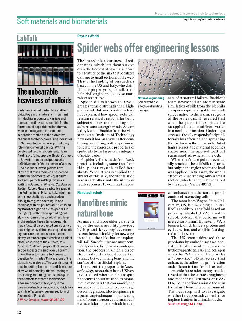
Natural engineeringSpider webs are effective at limiting damage.
The incredible robustness of spi-der webs, which lets them survive even the fiercest of storms, is down to a feature of the silk that localizes damage to small sections of the web. That’s the finding of researchers based in the US and Italy, who claim that this property of spider silk could help civil engineers to devise more robust structures.
Spider silk is known to have a greater tensile strength than high-grade steel. But previous studies have not explained how spider webs can remain relatively intact after being subjected to extreme loading such as hurricane-strength winds. A team led by Markus Buehler from the Mas-sachusetts Institute of Technology now says it has an answer after com-bining modelling with experiment to relate the nanoscale properties of spider silk to the large-scale integrity of spider webs.
A spider’s silk is made from basic proteins, including some that form thin, planar crystals called beta sheets. When stress is applied to a strand of this silk, the sheets slide across each other, until the silk even-tually ruptures. To examine this pro-
Nanotechnology
Physics World
Spider webs offer engineering lessons
cess of structural failure, Buehler’s team developed an atomic-scale simulation of silk from the Nephila clavipes – a species of golden orb-web spider native to the warmer regions of the Americas. It revealed that when the spider silk is subjected to an applied load, its stiffness varies in a nonlinear fashion. Under light stresses, the silk responds fairly uni-formly by softening and spreading the load across the entire web. But at high stresses, the material becomes stiffer near the applied load but remains soft elsewhere in the web.
When the failure point is eventu-ally reached, the stiff silk ruptures, but only in the region where the load was applied. In this way, the web is effectively sacrificing only a small section, which can then be repaired by the spider (Nature 482 72).
As more and more elderly patients enjoy the extra mobility provided by hip and knee replacements, researchers are looking for new ways to reduce the risk that an implant will fail. Such failures are most com-monly caused by poor osseointegra-tion, the process in which a direct structural and functional connection is made between living bone and the surface of an artificial implant.
In a recent study reported in Nano-technology, researchers in the US have investigated whether electrospun nanofibres could be used as biomi-metic materials that can modify the surface of the implant to encourage osseointegration. Electrospinning is a promising technique for fabricating nanofibrous structures that mimic an extracellular matrix, which in turn
Nanofibres mimic natural bone
can enhance the adhesion and prolif-eration of interacting cells.
The team from Wayne State Uni-versity, US, is developing a “bone-like” nanofibrous scaffold based on polyvinyl alcohol (PVA), a water-soluble polymer that performs well in electrospinning. However, PVA is bioinert, which hinders protein and cell adhesion, and exhibits fast deg-radation in water.
The US team addressed these problems by embedding two con-stituents of natural bone – nano-hydroxyapatite (nHA) and collagen – into the PVA matrix. This provides a “bone-like” 3D structure that enhances the adhesion, proliferation and differentiation of osteoblast cells.
Atomic force microscopy studies revealed that the surface roughness and mechanical stiffness of PVA/HA/Col nanofibres mimic those in the natural bone microenvironment. The next step will to investigate whether this approach can enhance implant fixation in animal models. Nanotechnology 23 115101
w
ISSN 0957-4484
NANOTECHNOLOGYVOLUME 23 NUMBER 11 23 MARCH 2012
iopscience.org/nano
Featured articleThe application of graphene as electrodes in
electrical and optical devices G Jo, M Choe, S Lee, W Park, Y H Kahng and T Lee

13
Special collection
Biomedical Engineering In response to the rapid pace of research in this vibrant and diverse field, IOP Publishing has launched an online collection, iopscience.org/biomedical-engineering, specially dedicated to showcasing papers that we feel make a particularly significant contribution to the biomedical engineering community.
The papers are taken from eight of our leading research publications, and cover everything from the bioprinting of cells for tissue-engineering applications, the development of biomaterials for soft- and hard-tissue regeneration, developing neural prostheses for restoring and enhancing memory, and developing a new diagnostic biomarker for chronic fatigue syndrome, to the latest developments in PET detector technology.
The collection also includes content from medicalphysicsweb which covers, in a highly accessible form, some of the most interesting and timely research published in the fields of medical physics and engineering.
Some articles from the collection:Evaluation of the tissue reaction to a new bilayered collagen matrix in vivo and its translation to the clinic Shahram Ghanaati et al 2011 Biomed. Mater. 6 015010
Toward engineering functional organ modules by additive manufacturingFrancoise Marga et al2012 Biofabrication 4 022001
A cortical neural prosthesis for restoring and enhancing memoryTheodore W Berger et al 2011 J. Neural Eng. 8 046017
Peripheral arterial volume distensibility: significant differences with age and blood pressure measured using an applied external pressureDingchang Zheng and Alan Murray2011 Physiol. Meas. 32 499
Fluid biopsy in patients with metastatic prostate, pancreatic and breast cancersDena Marrinucci et al 2012 Phys. Biol. 9 016003
The imaging performance of a LaBr3-based PET scannerM E Daube-Witherspoon et al 2010 Phys. Med. Biol. 55 45
Soft materials and biomaterialsiopscience.org/mater ials - sc ience
Materials science: from research to technology
The blood–brain barrier – which separates circulating blood from the brain extracellular fluid in the cen-tral nervous system (CNS) – often presents an obstacle for clinicians, since it is impermeable to medicines such as large-molecule neurotrophic factors that are used to treat CNS diseases. Traumatic brain injury can cause the barrier to be disrupted, potentially allowing molecules to be delivered to the injured area, but the extent of the opening depends on the trauma conditions and can change as the trauma develops.
Writing in the journal Nanotech-nology, researchers from the Shang-hai Jiao Tong University School of Medicine, China, describe how PBCA nanoparticles could effi-ciently deliver large molecules into the injured brain. In a rat model of traumatic brain injury, the team found that large-molecule horse-radish peroxidase on their own are unable to penetrate the post-trauma disrupted barrier. However, using the PBCA nanoparticles to deliver the molecules allowed large numbers to penetrate the barrier and reach the damaged area.
The ability of nanoparticles to
Nanoparticles deliver drugs into brainNanotechnology
Journal of Physics: Condensed Matter
transport material into the post-trauma brain was further confirmed by another experiment. In this case large-molecule enhanced green fluo-rescent protein (EGFP) was carried by PBCA nanoparticles across the disrupted blood–brain barrier, and more molecules were found to be distributed within the injured part of the brain when compared with EGFP molecules on their own.
The team also found that post-trauma the nanoparticle-delivered molecules reached the damaged region of the brain within 45 minutes. In contrast, under normal conditions it took 48 hours for PBCA nanopar-ticles to deliver even a small amount of EGFP into the brain. The scien-tists suggest that damaged blood ves-sels in the post-trauma brain make it easier for the PBCA nanoparticles to become attached the vascular walls, which speeds up the transport of large molecules into the brain. Nanotechnology 23 165101
Drug deliveryPBCA nanoparticle-mediated delivery of large-molecule EGFP into injured brain tissue.
Understanding the collective motion of self-propelling organisms in con-fined geometries, such as narrow channels, is of great theoretical and practical importance. For example, working out how active particles move through thin channels will be crucial for developing microfluidic devices that are able to control and sort motile cells. Moreover, study-ing the transport properties in these systems provides new and intrigu-ing examples of the very unusual behaviour of active matter, such as migration phenomena and the spon-taneous ratchet effect.
In an article for Journal of Physics: Condensed Matter, Luca Angelani and colleagues at La Sapienza Uni-versity in Rome, Italy, used numeri-
Simulations produce new insight into bacterial flow
cal simulations to study the motion of model bacteria in 2D channels under different flow conditions. The simulations indicate that the bacte-ria tend to accumulate on the chan-nel walls where they start swimming upstream. More intriguing is that the net bacterial flux can change from upstream to downstream, depending on the presence or absence of ran-dom tumble events in which each cell changes its own swimming direction.
Detailed analysis of the bacterial velocity and orientation allowed the scientists to quantify the effect by varying the cell density, channel width and fluid velocity. Based on this knowledge, the team developed a time-dependent flow protocol that can enhance the flux of bacterial cells through the channel. By performing periodic inversions in the direction of the solvent’s flow, this approach produced a particle flux that is three times greater than could be achieved with steady solvent flow. J. Phys.: Condens. Matter 24 065101
On the moveNew simulations show how active materials travel through narrow channels.

THIN FILM SURFACE ANALYSIS
l Instruments for residual gas analysis (RGA)l Evolved gas analysis l TPD/TPRl Vacuum process monitoring
PRECISION GAS ANALYSIS
l Static and dynamic SIMSl Chemical composition & depth profilingl SIMS for FIB including bolt-on modules
& integrated SIMS-on-a-Flangel Choice of primary ionsl Complete SIMS workstations
PLASMA CHARACTERISATIONl EQP ion mass and energy analyserl RF, DC, ECR and pulsed plasmal Neutrals and neutral radicalsl Time resolved analysisl HPR-60 extends analyses to
atmospheric pressure processes
QUADRUPOLES FORADVANCED SCIENCE
EQP Analyser
SIMS-on-a-Flange
QGA Gas Analysis System
Q u a d r u p o l e s f o r a d v a n c e d s c i e n c e
for further details of Hiden Analytical products contact:
H3_QuadsforAdvanced_IOP_A4_Materials_collection 19/10/2012 11:48 Page 1

15
iopscience.org/mater ials - sc ience
Materials science: from research to technology
Small is beautiful Sefaattin Tongay has grown graphene on silicon carbide to create this word “graphene”, which has features as tiny as 20 nm.
Graphene is the “wonder material” that could revolutionize electronics and possibly even replace silicon as the industry’s material of choice. Its unique properties arise partly from the fact that the electrons in graphene behave as if they have no rest mass, which means that they streak through the material at about 0.3% of the speed of light – an invaluable property in the quest for ultrafast transistors.
However, researchers must first be able to synthesize high-quality graphene in a controlled way. Two main approaches are currently being investigated: in the first the layer of graphene is deposited onto a copper film, while the second requires the graphene to be grown on a structured silicon-carbide surface.
Growing graphene on copper is more straightforward and allows the material to be produced over larger surface areas, but it produces a poly-crystalline layer with grain bounda-ries that can degrade the graphene’s electronic and mechanical properties. Growing graphene on silicon-carbide substrates is more expensive but ena-bles much smaller features to be pro-duced, such as arrays of 10 nm wide nanoribbons. The features are also produced without any jagged edges,
which maximizes electron mobility.The silicon-carbide technique has
been championed by Walt de Heer at the Georgia Institute of Technology in the US, who together with Claire Berger of the CNRS-Institut Néel in Grenoble, France, has guest edited a special issue of Journal of Physics D: Applied Physics focused on the epi-taxial growth of graphene on silicon carbide. “Silicon carbide is an impor-tant semiconductor in its own right, so graphene grown on this material can be used directly used in electron-ics applications,” he explained.
In the approach taken by de Heer’s group, the silicon-carbide crystal is heated to very high temperatures in a specially designed graphite ampoule. “This allows the growth rate of gra-
phene to be controlled and produces uniform samples,” he explains.
Technically, the graphene sam-ples can be grown as large as the silicon-carbide wafer – up to 100 mm – but smaller rectangles measuring 4–5 mm are preferred. “Bigger does not always mean better – it is all about quality,” says de Heer. “For electron-ics, well formed nanostructures on silicon carbide are much more inter-esting and important than very large, poorly formed sheets transferred from metals.”
Meanwhile, Sefaattin Tongay’s group at the University of California at Berkeley uses focused ion-beam lithography to implant ions in the silicon-carbide substrate, before loading the samples into a vacuum oven to finalize the growth process. Irradiating silicon carbide with ions creates open silicon and carbon bonds, explains Tongay, and during the annealing step the carbon rises to the surface and forms graphene.
“Our technique is good for writ-ing small features without too many complications,” he says. “We have currently made some further devel-opments and can now grow graphene even faster.” J. Phys. D: Appl. Phys. 45 15
Graphene growth hits the big timeS
ef T
onng
gay
Functional materials and nanomaterials
iopscience.org/jphysd
ISSN 0022-3727
Journal of Physics DApplied Physics
Volume 45 Number 15 18 April 2012
Special issueEpitaxial grapheneGuest Editors: Walt A de Heer and Claire Berger
Nanowire networks offer a route to making flexible and transparent electronics, and can be fabricated over large areas by depositing mate-rial from solution at room tempera-ture. In a recent study reported in the journal Nanotechnology, researchers from Middle East Tech-nical University in Ankara, Turkey, have used nanowire networks to create a fully flexible photodetec-tor that achieves very fast response
characteristics and a recovery time of less than 10 ms.
The active semiconducting ele-ment of the photodetectors consists of a network of germanium nano- wires. A high-temperature vapour transport method is used to synthe-size the nanowires, which can then be taken into solution and deposited onto various substrates in the form of a network with controllable density.
Nanowire networks are also used for the contacts to create devices that are fully flexible, but this time they are made from spray-coated silver nanowires that are synthesized through a polyol process. As part of the study, contacts made from net-works of single-walled carbon nano-
tubes were also investigated. Metal-semiconductor-metal pho-
todetectors were fabricated both on glass and flexible PET substrates. Junctions between germanium nanowires allow barrier-dominated conduction in the network, which the team found to be responsible for the fast response and recovery time of the device.
In this study the researchers oper-ated the device under solar-simulated light, and they will now investigate the near-infrared response of the ger-manium nanowire networks. They also plan to explore the use of germa-nium nanowire networks as the active material in thin-film transistors. Nanotechnology 23 325202
Nanowires speed up light detectors
Nanotechnology ISSN 0957-4484
NANOTECHNOLOGYVolume 23 Number 32 17 August 2012
iopscience.org/nano
Featured articleNanostructured porous silicon films for terahertz optics
Michael Riley, Albert Redo-Sanchez, Panagiotis Karampourniotis, Joel Plawsky
and Toh-Ming Lu

Functional materials and nanomaterials
16
iopscience.org/mater ials - sc ience
Materials science: from research to technology
LabTalk
Stepped substrate generates ordered nanostripesLow-dimensional oxide systems offer a unique playground for studying the physics of materials in reduced dimensions, and could be important for a number of emerging applications in nanotechnology. Self-organization of oxide nanostructures at metal surfaces is an attractive design route, since it offers simple and reproducible methods for engineering novel materials with no bulk analogues.
In a study reported in Journal of Physics: Condensed Matter, a team led by Falko Netzer of Karl-Franzens University Graz, Germany, has shown that a stepped metal substrate can steer the formation of a highly ordered superlattice of manganese oxide nanostripes, a finding that could be important for designing tailored nanostructures and for exploring new strategies in nanotechnology fabrication.
In the experiments, the researchers use a Pd(1 1 17) surface with (001)-terraces to drive the stabilization of a two-dimensional c(4 × 2) Mn3O4 phase. While the long-range order of this phase is poor on the flat Pd(001) surface, a highly ordered superlattice of oxide nanostripes forms on the stepped surface. The superlattice periodicity is different from the step periodicity of the original Pd(1 1 17) template, but instead corresponds to the restructuring of the substrate into Pd(1 1 21).
Extensive ab initio density functional theory calculations revealed the physical origin of this phenomenon. In the nanostripes made by building up subsequent rows of the c(4 × 2) monolayer, the stable oxide configurations are terminated by MnO2 units at both sides of the stripes. The most stable stripes cannot be accommodated on the (1 1 17) surface, but there is enough space on the (1 1 21) terraces – and this drives the terrace reorganization.
Future work will investigate the electronic and magnetic properties of these phases.J. Phys.: Condens. Matter 24 042001
New nanoparticles TEM images show a range of structures produced using corrosion processes.
Researchers in Spain have invented a new technique for making hollow nanoparticles with sophisticated shapes and compositions. The method, which combines two well known corrosion processes into a single step, modifies the shape of tiny nanoparticles after they have been created.
Edgar Gonzàlez and colleagues at the Institut Català de Nanotec-nologia have shown that well known corrosion processes can be used to attack and pit nanoparticles from the inside out, leading to complex geometric interconnected multicav-ity hollow nanostructures.
Using this technique, the team was able to produce structures with (a) spherical, (b) cubic and (c) cylindri-cal shapes, shown here as transmis-sion-electron-microscope images and accompanied by drawings that represent the morphology of each nanostructure. The structures can also range in shape from molecular labyrinths or nanomazes (made from
Physics World
Corrosion carves out 3D nanostructures
silver and gold or platinum) to gold fullerenes. Other structures, such as nanoboxes, porous nanotubes and nanoframes, can even be fashioned from silver and gold nanoparticles.
The resulting nanostructures could find use in drug delivery, catalysis and even as structural components for nanorobots, and the researchers claim that the technique can also be readily adapted to industrial-scale production levels (Science 334 1377).
Vict
or P
unte
sa
b
c
The electronic properties of gra-phene, including high carr ier mobilities, long carrier mean-free paths, polarizability in proximity to a magnetic substrate and long spin diffusion lengths, have exciting potential for charge- or spin-based device applications. First, however, scientists must devise practical and scalable methods to grow graphene directly on dielectric substrates.
Writing in Journal of Physics: Con-densed Matter, a team of US research-ers explain how they have used molecular beam epitaxy to deposit graphene in a controlled manner on Co3O4(111).
The single- or few-layer graphene was grown on an oxide heterojunc-tion structure: a few-layer Co3O4(111) film on a thin Co(111) film on a sap-phire(0001) substrate. Auger and low-energy electron diffraction data reveal the formation of large-domain graphene – (111)-ordered sp2 carbon films – on the oxide substrate at cov-erages as low as 0.4 monolayers up to
at least three monolayers. The graphene/oxide interface is
incommensurate, but the graphene layers are in registry with each other. Core-level photoemission and spec-troscopic ellipsometry measure-ments indicate that the graphene layers display electronic properties similar to those of graphene grown on SiC(0001) or transferred to SiO2, but with significant graphene-to-oxide charge transfer.
Graphene on this oxide hetero-structure is predicted to become spin polarized. Although Co3O4 is para-magnetic, and Co is ferromagnetic at room temperature, the proximity between the Co ions and the gra-phene conduction electrons could result in spin polarization of the graphene if the Co3O4 layer is thin enough. As a result, the research-ers believe that the work could lead to new opportunities for industrial-scale development of charge- and spin-based devices.J. Phys.: Condens. Matter 24 072201
Applications beckon for graphene spintronicsJournal of Physics: Condensed Matter
iopscience.org/jpcm
ISSN 0953-8984
Journal of PhysicsCondensed MatterJournal of Physics
w
Volume 24 Number 7 22 February 2012
Topical reviewsCalculation of dispersion energiesJohn F Dobson and Tim Gould
Nano-plasmonic antennas in the near infrared regimeN Berkovitch, P Ginzburg and M Orenstein

17
Special collections
MetamaterialsRepresenting one of the most active and interdisciplinary areas of materials science today, research on metamaterials continues to attract the attention of wide-ranging communities including condensed matter physics, electrical engineering, optics, nanoscience, semiconductor engineering and more.
In particular, their significant promise in terms of potential applications means that metamaterials look set to play a pivotal role in technological advances for years to come.
A collection of papers from several of IOP Publishing’s leading research publications have been brought together at iopscience.org/metamaterials.
Featured articles include:Surface whispering-gallery modeJ J Yang, M Huang, J Yu and Y Z Lan2011 EPL 96 57003
Experimental demonstration of a broadband array of invisibility cloaks in the visible frequency rangeV N Smolyaninova, I I Smolyaninov and H K Ermer2012 New J. Phys. 14 053029
GrapheneApplications that graphene cannot accommodate seem to be few and far between. As the field matures, the material continues to reveal more exotic properties, inspiring research in both fundamental physics and technology.
Recognizing the rapid pace of research, IOP Publishing has launched an online collection at iopscience.org/graphene to showcase papers covering the field in all aspects including the latest advances in technology, experiment and device development, as well as a number of topical reviews.
Papers include:Graphene prehistoryA K Geim2012 Phys. Scr. 2012 014003
Electronic properties of graphene nanostructuresF Molitor, J Güttinger, C Stampfer, S Dröscher, A Jacobsen, T Ihn and K Ensslin2011 J. Phys.: Condens. Matter 23 243201
Functional materials and nanomaterialsiopscience.org/mater ials - sc ience
Materials science: from research to technology
Carbon dots are light-emitting nanoparticles that can be used to track biological processes inside cells. They are less toxic than similar alternatives, making them more suit-able for use in live biological systems, but the light-emitting properties of current versions are not ideal.
Most attempts to make carbon dots have required the particles to be coated with other molecules to achieve useful luminescence. In work reported in Science and Technology of Advanced Materials, a team led by Amita Pathak at the Indian Institute of Technology has produced water-soluble carbon dots that selectively emit light across the entire visible range, but do not need any surface coating.
The team produced the carbon dots by using microwaves to break down dextrin, a low-molecular-
weight carbohydrate, and found that the resulting nanoparticles emit dif-ferent colours of light when excited by specific wavelengths. It remains unclear how this multi-coloured lumi-nescence arises, but it allows precise control of the light emission that can be tailored to specific applications.
To ensure that the carbon dots were non-toxic, the team added different concentrations of the nanoparticles to cultured cells. Increasing the con-centration of carbon dots made little difference to cell survival, showing that they are safe to use in live tissue.
The properties of these new carbon dots make them ideal for bioimaging applications and medical diagnostics. The researchers have already begun to look at their potential for investi-gating interactions between drugs and cells.Sci. Technol. Adv. Mater. 13 045008
Brighter future for carbon dotsScience and Technology of Advanced Materials
High-temperature electrochemi-cal gas sensors can help to improve energy efficiency and reduce the emission of pollutants when used as part of feedback control systems in vehicles, coal-fired power plants and other applications. The sensitivity of such sensors is highly dependent on the material composition and archi-tecture of the sensing electrodes, which must have a large surface area, high porosity and fast electron trans-port. One-dimensional nanomateri-als represent ideal candidates, but manufacturing challenges present a barrier to commercialization.
Writing in the journal Nanotech-nology, Nick Wu and his team at West Virginia University, US, explore whether sensor electrodes made of La0.8Sr0.2MnO3 nanofibres could address some of these issues.
Nanotechnology
Nanofibres sense the future
The group found that, compared with conventional micron-sized pow-ders, the nanofibres have a larger spe-cific surface area and form a porous network that facilitates gas diffu-sion. In addition, the nanofibres are interconnected and form a continu-ous path for charge transport. This unique architecture increases the electrochemical reaction sites, and as a result the sensor exhibits enhanced sensitivity, lower detection limits and a faster response to the change in the gas concentration.
The team showed that a sensor with a nanofibre-based electrode can successfully detect carbon monoxide at temperatures above 500 °C, which indicates that this approach offers an effective route for improving the performance of high-temperature electrochemical sensors. Nanotechnology 23 305501
Better detector A sensor electrode constructed from numerous electrospun nanofibres with a diameter of around 200 nm.
ISSN 1468-6996
iopscience.org/stam
Editor-in-Chief Teruo Kishi
Published by the National Institute for Materials Science in par tnership with IOP Publishing
Science and Technologyof Advanced Materials
Promotional copy fromScience and Technology of Advanced Materials, Vol 12 (2011) Issue 6
Focus on new Materials MiMicking nature
Science and Technology of advanced MaTerialS
Focus articles selection December 2011
Prom
otional copy
Sign up to the newswire for updates on the emerging and key applications of nanotechnology, and the very latest tools and materials.

P I E Z O N A N O P O S I T I O N I N G
P I - M I C R O S C O P Y
PIFOC® – Scans and Positions Objectives
Travel ranges to 1 mm
Resolution in the nanometer range
Minimum settling time
M-687 – Low-Profile, Precision XY Stage
Travel ranges to 135 mm
Minimum incremental motionup to 0.1 μm, highly stable
Velocity to 120 mm/s
P-545 – Dynamic Motion in 3 Axes
Travel ranges to 500 μm
Resolution in the nano meter range
Response time in the range of a few milliseconds
Positioning SystemsF O R M I C R O S C O P Y
For more information, contact us: [email protected] · www.pi.ws
Physik Instrumente (PI) GmbH & Co. KGTel. +49 (721) 4846-0
Positioning systems from PI are particularly suited for the
most challenging applications in microscopy, life science, bio-
technology or medical technology. They offer subnanometer
resolution, large travel ranges and they are extremely fast.
pi_120937_kombi_m2_193x262_en.indd 1 22.10.12 15:12BLEED.indd 1 22/10/2012 14:49

19
iopscience.org/mater ials - sc ience
Materials science: from research to technology
Topological insulators are a new state of quantum matter that exhibit a bulk energy gap and spin-polarized sur-face states that give rise to a range of novel electronic properties. Potential applications include spintronics and fault-tolerant quantum computation.
A number of materials have been shown to be topological insula-tors. Bismuth-based binary com-pounds such as Bi2Se3 and Bi2Te3 have attracted particular attention because of their relatively large bulk gaps and simple non-trivial surface states. However, doping in these sys-
tems makes it almost impossible to measure the transport properties of their unique surface states because of the large numbers of charge carri-ers present at the surface.
In contrast, Bi2Te2Se – a newly discovered ternary tetradymite com-pound – offers a promising alter-native as a result of its structural perfection and naturally large bulk resistivity. In an article in Journal of Physics: Condensed Matter, research-ers at Zhengzhou Normal University, China, report first-principles calcu-lations of the electronic structures of
Bi2Te2Se thin films based on density-functional theory, which identify top-ologically protected surface states of the system.
The researchers calculate that intrinsic Bi2Te2Se thin films of three or more quintuple layers exhibit an electronic structure with a robust topological nature. The findings pave the way for an experiment to measure the transport properties of an intrinsic topological insula-tor using a device fabricated with Bi2Te2Se thin films.J. Phys.: Condens. Matter 24 035502
Topological insulators: fabricating devices without dopingJournal of Physics: Condensed Matter
Sky highThe Tokyo Sky Tree, at 634 m the tallest sightseeing and TV broadcasting tower in the world, relies on the most advanced TMCP steels.
Although steel was first produced about 4000 years ago, scientists are still exploring new ways to improve its performance as today’s construction material of choice. China dominates basic steel production, accounting for about 45% of global output, while Japan – the world’s second largest steel producer – is shifting its focus towards the manufacture of higher-grade steels.
One key advance originally pio-neered in Japan is the water-cooled thermomechanical control process (TMCP), which yields stronger and tougher steels than is possible with conventional water-cooled steel-plate processes. TMCP steels with added alloys are also easier to weld, and as a result they are highly valued in industries such as shipbuilding, offshore structures, pipelines and building construction.
Kiyoshi Nishioka and Kazutoshi Ichikawa of Nippon Steel Corpora-tion, Japan’s largest steel producer, describe recent developments in TMCP technology in a review arti-cle for Science and Technology of Advanced Materials. They explain that TMCP combines controlled
rolling, which enhances toughness by refining the steel’s microstructure, with an accelerated cooling phase that drives a phase transformation to ferrite and bainite. It’s this trans-formation that yields a high tensile strength, which can be controlled from 500 to more than 800 MPa.
The addition of microalloys, such as trace amounts of niobium, also strengthens the steel. This is because precipitates of niobium form within the ferrite matrix during cooling, which both distorts and hardens the lattice structure. According to Mish-ioka and Ichikawa, recent neutron
scattering experiments reveal that the presence of niobium also raises the ferrite transformation temperature.
Recent improvements to TMCP technology has helped to achieve more uniform cooling, which mini-mizes strain in the steel plate. Nippon Steel has developed and commercial-ized CLC-µ, which has reduced the temperature variation by 50%, while another process known as Super-OLAC has also delivered similar results. Stronger and tougher steels have also been produced by reducing impurities through hot-metal and vacuum degassing processes, and using computational design methods to optimize the TMCP process.
Research projects have also shown that the superfine grain structure can be controlled through a combination of heavy-reduction rolling with accel-erated cooling during the rolling pro-cess. There have also been attempts to use copper in high-strength steels, while novel fine microstructures such as acicular ferrite are expected to improve toughness and the steel’s resistance to hydrogen-induced cracking. Sci. Technol. Adv. Mater. 13 023001
High-grade steels reach new heights
iopscience.org/jpcm
ISSN 0953-8984
Journal of PhysicsCondensed MatterJournal of Physics
Featured in this issueLiquids, Soft Matter and Biological Physics
w
Volume 24 Number 3 25 January 2012
Structural and advanced materials

Structural and advanced materials
20
LabTalk
Knee device hints at end for batteriesBattery-powered devices could soon be a thing of the past, thanks to a group of UK researchers who have created a novel energy harvester to power some of the latest wearable gadgets. Writing in the journal Smart Materials and Structures, the researchers say that strapping the energy harvester to the knee joint could deliver enough power when walking to operate body-monitoring devices such as heart-rate monitors, pedometers and accelerometers. Soldiers may find the device particularly useful, since they often need to carry up to 10 kg of battery equipment when on foot patrol.
The energy harvesting device, which fits onto the outside of the knee, is circular and consists of an outer ring and central hub. The outer ring rotates as the knee joint goes through a walking motion, and is fitted with 72 plectra that “pluck” four energy-generating arms – known as bimorphs – attached to the inner hub.
“A bimorph is a type of piezoelectric device capable of converting mechanical energy, such as the vibrating caused by the plectra, into electrical energy, and vice versa,” said Michele Pozzi, the lead author of the study, who at the time was at Cranfield University. Pozzi explains that the knee generates lots of energy because it moves through large angles during walking, and at relatively high speed.
At the moment the device can harvest around 2 mW of power but the researchers believe that with a few realistic improvements it could generate more than 30 mW – enough for next-generation GPS tracking, more advanced signal processing and more frequent and longer wireless transmission.
“There is an on-going project looking at manufacturing a more compact and truly wearable harvester. I’d put a price tag of less than £10 for each harvester in large-scale production,” continued Pozzi. The ultimate aim of the project is to reduce the heavy battery burden on dismounted soldiers.Smart Mater. Struct. 21 075023
iopscience.org/mater ials - sc ience
Materials science: from research to technology
Robojelly The robotic device flaps its bell using a clever combination of materials.
A robotic swimmer, dubbed “Robo-jelly”, that mimics the motion of a jel-lyfish has been built by researchers in the US. The hydrogen-powered device, which propels itself using an “artificial muscle”, could be used in a number of scientific, military and commercial marine applications, the researchers claim.
Robojelly has been built by a team led by Yonas Tadesse of the Univer-sity of Texas, Dallas that is claiming “the first successful powering of an underwater robot using external hydrogen as a fuel source”. As well as only producing water as a waste prod-uct, hydrogen is an attractive fuel for remote marine vehicles because it could, in principle, be obtained from seawater using energy from the Sun.
At Robojelly’s heart is a com-mercially available nickel–titanium shape-memory alloy (SMA) – a deformable material that returns to its original shape when heated. The SMA is wrapped in a sheet of carbon nanotubes that is itself coated with titanium particles, which catalyse the reaction between hydrogen and oxy-gen. The heat produced as a result of this oxidation then allows the SMA to revert to its original shape. Carbon nanotubes are used because they are slightly porous, thus allowing the hydrogen and oxygen to reach the catalyst.
The robot has an umbrella-like structure that mimics the propul-sion strategy of the common jel-lyfish Aurelia aurita. The “bell” of the robot is made from silicone and is supported by eight springy steel ribs, with a string running alongside each rib from the edge of the bell to a
Smart Materials and Structures
Robot jellyfish fuelled by hydrogen
pulley at its centre. To demonstrate Robojelly in
action, the team placed it in a tank of water. A fixed amount of hydrogen and oxygen was then introduced to the tube, which warmed up the SMA and made it change shape. As it reformed, the alloy pulled on the strings, caus-ing the bell to flap in one direction. As the SMA cooled, the restoring force of the steel ribs made the bell flap in the opposite direction. According to the team, an entire motion cycle can occur in less than 10 s.
The team measured the deforma-tion of the bell to be about 14%. This is smaller than the 29% achieved when the robot was electrically pow-ered and substantially less than the 42% that is typical of a real jellyfish. Although the researchers have so far only operated the robot jellyfish when it was clamped at the bottom of a water tank, they are looking at ways of boosting the performance and efficiency of the system.Smart Mater. Struct. 21 045013
Publish your latest research with SMS,with receipt to acceptance in four months
iopscience.org/sms
Smart Materials and StructuresSystems from nano- to macroscale
ww
iopscience.org/sms
ISSN 0964-1726
Smart Materialsand StructuresSystems from nano- to macroscale
w
Volume 21 Number 5 May 2012
Topical reviewA review of stimuli-responsive polymers for smart textile applicationsJinlian Hu, Harper Meng, Guoqiang Li and Samuel I Ibekwe

21
Structural and advanced materialsiopscience.org/mater ials - sc ience
Materials science: from research to technology
Recent developments in aircraft design have led to a dramatic rise in the use of composites, and struc-tural adhesive bonding has emerged as the most attractive technique for joining together aircraft components that are made from similar/dissimi-lar composites and metals. Com-pared with welding and mechanical fastening, adhesive bonding offers substantial weight reduction, low bonding temperature and uniform stress transfer – rather than the highly localized point contacts that are typical of mechanical fastening.
When used to join together the pri-mary structures that carry the flight load, any failure of these adhesive bonds would be so catastrophic that the aircraft could be lost altogether. A strategic research initiative has therefore been formed to investigate whether “smart” adhesives have the potential to monitor an aircraft’s pri-mary structures for cracks, delami-nation and other sources of failure.
The team, led by Shaker Meguid from the Mechanics and Aero-space Design Lab at the University of Toronto, Canada, explain their approach in an article for Nano-technology. The idea is to convert polymeric thermoset adhesive resins into multifunctional materials that perform multiple “structural” and “non-structural” functions at the same time.
This multifunctionality is achieved by dispersing very small amounts
Smart adhesives detect aircraft failureNanotechnology
Flight schoolSmart adhesives could detect early failure in modern aircraft.
(0.1–2%) of carbon nanotubes and nanowires in the resin, which is expected to deliver a significant improvement in the adhesive’s electromechanical properties. Using theoretical models based on net-work recognition rather than earlier Monte Carlo simulations, the group is currently investigating the effect of uniformly dispersed, aligned and agglomerated carbon nanotubes on the electrical conductivity of the mul-tifunctional nanocomposites.
The results of the study, which are in good agreement with exist-ing experimental work, reveal that the highest electrical conductivity occurs when the nanotubes are par-tially rather than perfectly aligned. The data also show that the presence of agglomerated nanotubes raises the conductivity at and close to the percolation threshold, but limits the increase in conductivity at higher nanotube concentrations.
The group’s results provide a new, robust and computationally effi-cient model that can be adopted as a predictive tool to characterize and evaluate electrical conductivity in multifunctional nanocomposites.Nanotechnology 22 485704
New horizons in adaptive and active materialsSmart Materials and Structures
ww
iopscience.org/sms
ISSN 0964-1726
Smart Materialsand StructuresSystems from nano- to macroscale
w
Volume 21 Number 9 September 2012
Adaptive and active materials: Selected papers from the ASME 2011 Conference on Smart Materials, Adaptive Structures and Intelligent Systems (SMASIS 11) (Scottsdale, AZ, USA, 18–21 September 2011)Guest Editors: Diann Brei, Stefan Seelecke, Nancy Johnson, Zoubeida Ounaies, Hani Naguib, John Huber, Travis Turner, Michael Philen and Vishnu Baba Sundaresan
A special issue of Smart Materials and Structures focuses on recent advances in adaptive and active materials, as reported at the Confer-ence on Smart Materials, Adaptive Structures and Intelligent Systems (SMASIS) in Scottsdale, USA.
The articles reveal how under-standing the behaviour and mechan-ics of these novel materials can guide the development of new material systems, an approach that has helped to improve shape-memory metals and polymers, ferroelectrics, ferro-magnetics, and more recently multi-
ferroic materials. Multifunctional materials, a new generation of active materials that integrate structural, sensing, and actuation components into the material system, are also featured in the issue.
A natural extension of these multi-functional materials is a new class of bio-inspired materials, which range from detailed bio-mimicry of sens-ing and self-healing materials to nano- and microstructures that take advantage of features observed in biological systems.Smart Mater. Struct. 21 9
If the traffic noise outside your office annoys you, then help could be at hand in the form of a new type of cur-tain that absorbs sound while allow-ing natural light to pass through. The material for the curtain has been de veloped by researchers at the Swiss Federal Laboratories for Materials Science and Technology (Empa) and can absorb up to five times as much sound as a typical lightweight curtain.
Materials such as glass and con-crete that are used in most buildings are acoustically “hard”, which means they reflect sound waves rather than reduce noise. However, acoustic ally “soft” materials absorb some of the sound energy that strikes them.
The Empa researchers designed the ma terial using a computer model to predict the acoustic behaviour of a variety of curtains. Properties such as size, porosity and mass per unit area were altered to maximize sound absorption over a wide range of frequencies. Annette Douglas, a textile de signer, then used the model to weave together four or five differ-ent modified polyester yarns.
The material was tested using Empa’s re verberation chamber. With the curtain positioned 15 cm from a wall, the researchers found that at low frequencies of 200 Hz it absorbed a fifth of the incident sound energy, a factor that rose to 75% above 500 Hz, where the human ear is at its most sensitive. The curtains are now being commercially produced by silk wea-vers Weisbrod Zürrer.
Curtains for noisePhysics World
SOME ARTICLES IN THIS ISSUE
Autonomous stimulus triggered self-healing in smart structural compositesC J Norris, J A P White, G McCombe, P Chatterjee, I P Bond and R S Trask Smart Mater. Struct. 21 094027
Switching behavior of ferroelectric thin films with dead layersYifan Xia and Jie Wang Smart Mater. Struct. 21 094019
Deformation and instabilities in dielectric elastomer compositesWenyuan Li and Chad M Landis Smart Mater. Struct. 21 094006

Our vacuum systems simply offer more. Your process will be improved by the performance of our systems!UNIVEX 250 are suitable for the production of functional coatings, resp. coating systems, thermal, e-beam and organics evaporation or RF/DC sputtering. All deposition principles are possible as single or combined processes. UNIVEX 250 are cost-effective starter systems, easy to extend or retrofi t.
www.myunivex.com
UNIVEX 250Small, but powerful!
Compact thin fi lm deposition system
©B
ICO
M_1
1618
.02
3.10
.201
2
Oerlikon Leybold Vacuum GmbHBonner Strasse 498D-50968 KölnT +49 (0)221 347-0F +49 (0)221 347-1250E-mail : [email protected]://www.oerlikon.com/leyboldvacuum
Compact Box Coater for manual or semi-automatic coating processes in research, development and pilot production
Anz_UNIVEX250_PW_EN 2012.indd 1 17.10.12 15:24

23
iopscience.org/mater ials - sc ience
Materials science: from research to technology
The latest nanoscale fabrication technology regularly produces cutting-edge materials and novel electronic devices, and scientists rely on first-principles calculations to fully understand the electronic con-figurations and transport properties within them. Introducing practical and tractable calculation methods that accurately describe the phys-ics in nanostructures suspended between electrodes has therefore become an imperative.
In an article for Journal of Phys-ics: Condensed Matter, a team of Japanese researchers describe a new ab initio simulation method that harnesses the power of massively
parallel computers to investigate electron transport within nano-structures. Such high-performance computing techniques are becoming more important as researchers seek to study more complex systems, typi-cally characterized by many atoms of different chemical species in open, low-symmetry structures.
The new algorithm combines a real-space finite-difference (RSFD) formalism with the overbridging boundary-matching (OBM) method. The researchers explain that the RSFD approach does not suffer from artificial periodicity, which can affect methods that exploit plane-wave basis sets, or the linear depend-
ence problems that occur when using atomic basis sets.
The researchers find that the com-bination of RSFD and OBM methods makes it possible to execute first-principles transport calculations using large models. To demonstrate the advantages of the technique, they present several examples of transport calculations in systems ranging from jellium nanowires to the tip-and- surface system in a scanning tunnel-ling microscope. They believe that the technique could be used in the near future to design nanomateri-als that are destined for use in mass- produced electronic devices.J. Phys.: Condens. Matter 23 394203
Supercomputers power nanomaterial designJournal of Physics: Condensed Matter
Model approachThis atomistic simulation shows the interaction of a basal dislocation with a twin boundary.
Numerical methods have become an essential tool for investigating and designing new materials, and a special issue of Modelling and Simulation in Materials Science and Engineering fea-tures a series of articles that explain how modelling is used alongside the-ory and experiment to understand the properties of polycrystals. Topics cov-ered in the issue include the crucial relationship between the microstruc-ture and properties of these materials, as well as the effects of deformation such as single-crystal anisotropy and microstructure evolution.
The articles have been selected from the invited presentations at a special symposium organized to honour the huge contributions made to this field by Carlos Tomé of the Los Alamos National Laboratory in the US. Throughout his career, Tomé pioneered the development of theoretical and numerical models of polycrystals, with particular focus on the role played by texture and micro-structure on the anisotropic behav-iour of engineering materials.
Tomé’s influence has been critical in establishing a strong connection between simulation and experiments, and in bridging different scales when integrating robust multiscale models with experimental results. It’s fitting, then, that this collection of articles are representative of the range of length-scales, materials, and experimental and modelling techniques discussed at the symposium. As an example, Tomé’s group at Los Alamos report on synchrotron X-ray measurements of lattice strains in hexagonal-close-packed iron polycrystals, and how polycrystal plasticity models are used to interpret the results.Modelling Simul. Mater. Sci. Eng. 20 2
Simulations probe polycrystals
iopscience.org/jpcm
ISSN 0953-8984
Journal of PhysicsCondensed MatterJournal of Physics
Featured in this issueSurface, Interface and Atomic-Scale Science
w
Volume 23 Number 39 5 October 2011
Topical reviewSingle ion induced surface nanostructures: a comparison between slow highly charged and swift heavy ionsFriedrich Aumayr, Stefan Facsko, Ayman S El-Said, Christina Trautmann and Marika Schleberger
Special sectionAtomically controlled fabricationGuest Editors: Yuji Kuwahara and Hideaki Kasai
Synthesis, characterization and modelling methods
SOME ARTICLES IN THIS ISSUE
Atomic structures of symmetric tilt grain boundaries in hexagonal close packed (hcp) crystalsJ Wang and I J Beyerlein Modelling Simul. Mater. Sci. Eng. 20 024002
Texture and elastic strains in hcp-iron plastically deformed up to 17.5 GPa and 600 K: experiment and modelSébastien Merkel, Marion Gruson, Yanbin Wang, Norimasa Nishiyama and Carlos N Tomé Modelling Simul. Mater. Sci. Eng. 20 024005
Low-strain plasticity in a high pressure die cast Mg–Al alloyK Vanna Yang, C H Cáceres, A V Nagasekhar and M A Easton Modelling Simul. Mater. Sci. Eng. 20 024010

Synthesis, characterization and modelling methods
24
iopscience.org/mater ials - sc ience
Materials science: from research to technology
HighlightMapping out crystal structurePredicting the crystal structure of an alloy or a compound from its constituent chemical elements has long been a challenging subject for materials research. The structure map, or structural stability diagram, has played an effective role as an a priori guide for finding possible stable phases, but new approaches are needed to reflect the large number of parameters that influence crystal chemistry.
Various mapping schemes have been proposed, each of which identifies a number of key parameters related to electronic or crystal-structure information. This yields a diagram that maps out the relative position of different structure types, and an attempt can then be made to see if there is a strong correlation between specific crystal-structure types and the selected set of parameters.
However, 2D and 3D structure maps can’t properly represent all of the parameters associated with crystal chemistry. In an article for Computational Science and Discovery, a team of Japanese, Swiss and US researchers provide a new approach that explores the collective impact of all relevant chemical and bonding parameters on the phase stability. To demonstrate the effectiveness of the scheme, they use a database of AB2-type intermetallics to develop a classification scheme of phase stability.
The new approach exploits the principles of information entropy. Key parameters that link the nature of constituent building units with structural stability are systematically identified, and the contribution of each one is mapped onto a multidimensional array of parameters. The team then use a quantitative scaling parameter to identify the dominant attributes, allowing the multidimensional array to be mapped onto a low-dimensional structure diagram for easy visualization.
This new form of structure map provides a means for exploring a multivariate array of attributes associated with structural stability, and also for investigating the effectiveness of conventional mappings for crystal chemistry. Since the new technique makes no prior assumption of the attributes governing phase stability, the researchers believe that it provides a more objective method of exploring classification schemes in crystal chemistry.Comput. Sci. Disc. 5 014009
A new group of materials called “gra-phynes” have been discovered by researchers in Germany. Graphyne, like graphene, is a sheet of carbon just one atom thick, but whereas graphene only exists with a honeycomb lattice structure, graphynes can assume sev-eral different 2D structures.
Although only molecular amounts of the material have currently been synthesized, Andreas Görling and colleagues at the University of Erlangen-Nürnberg say that gra-phynes have “Dirac cones” – a fea-ture in their band structure that was previously thought to be unique to graphene. Dirac cones – where the conduction and valence bands meet in a single point at the Fermi level – contribute to graphene’s unusual electronic properties because its electrons behave as though they
are relativistic particles with no rest mass, and so can whizz through the material at extremely high speeds. Now, computer simulations of the band structure of three graphynes –α -graphene, β -graphene and 6,6,12-graphyne – using density-functional-theory calculations show the presence of Dirac cones in each. While the first two graphynes have hexagonal structures, the structure of the third is rectangular.
Interestingly, because of the rec-tangular symmetry of 6,6,12-gra-phyne, it should have electronic properties that will vary in different directions along its plane so that the conductance depends on the direc-tion of the current. This directional dependence, which is not seen in gra-phene because it is almost isotropic, could be useful in future nanoscale devices. Graphyne also appears to have two different Dirac cones lying slightly above and below the Fermi level, meaning that it is “self-doped” and so could be used as a semicon-ductor in electronic devices (Phys. Rev. Lett. 108 086804).
Faster scanningImages acquired by (a) raster scanning and (b) Lissajous curves.
Non-raster scan trajectories have the potential to significantly speed up the imaging process in scanning probe microscopy (SPM), and also offer other advantages over con-ventional raster scanning. Writing in Nanotechnology, Tomas Tuma of IBM Research Zurich introduces a new non-raster scan trajectory for high-speed SPM in which the scanner traces a so-called Lissajous curve.
Although Lissajous curves only require two single-tone actuation frequencies, the resulting trajectory covers a rectangular image area in a high-resolution grid-like pattern. Furthermore, owing to their unique multi-resolution property, Lissajous scan trajectories provide a preview of the entire image area in fractions of the overall scan time, with a spa-tial resolution that continuously increases until the complete image has been obtained.
Scan trajectories based on Lissa-jous curves have been studied previ-ously for medical imaging. The key advantage of Lissajous scan trajec-tories is that they can be enabled using extremely narrow-band actua-
Graphyne: the next wonder material?
Physics World
Nanotechnology
Lissajous curves speed SPM imaging
tion signals, which do not excite any unwanted dynamics of the mechani-cal scanning device.
In a high-speed SPM, a pure sin-gle-tone frequency is used to actuate the SPM scanner in each of the two in-plane axes. Owing to the inter-ference between the two actuation frequencies, the scanner traces an elegant and smooth grid-like pat-tern. Also, with their narrow-band frequency spectrum, Lissajous trajectories can benefit from tail-ored scanner designs and control architectures with improved noise resiliency.Nanotechnology 23 185501
GraphyneThese 2D carbon-based materials could have exotic electronic properties.
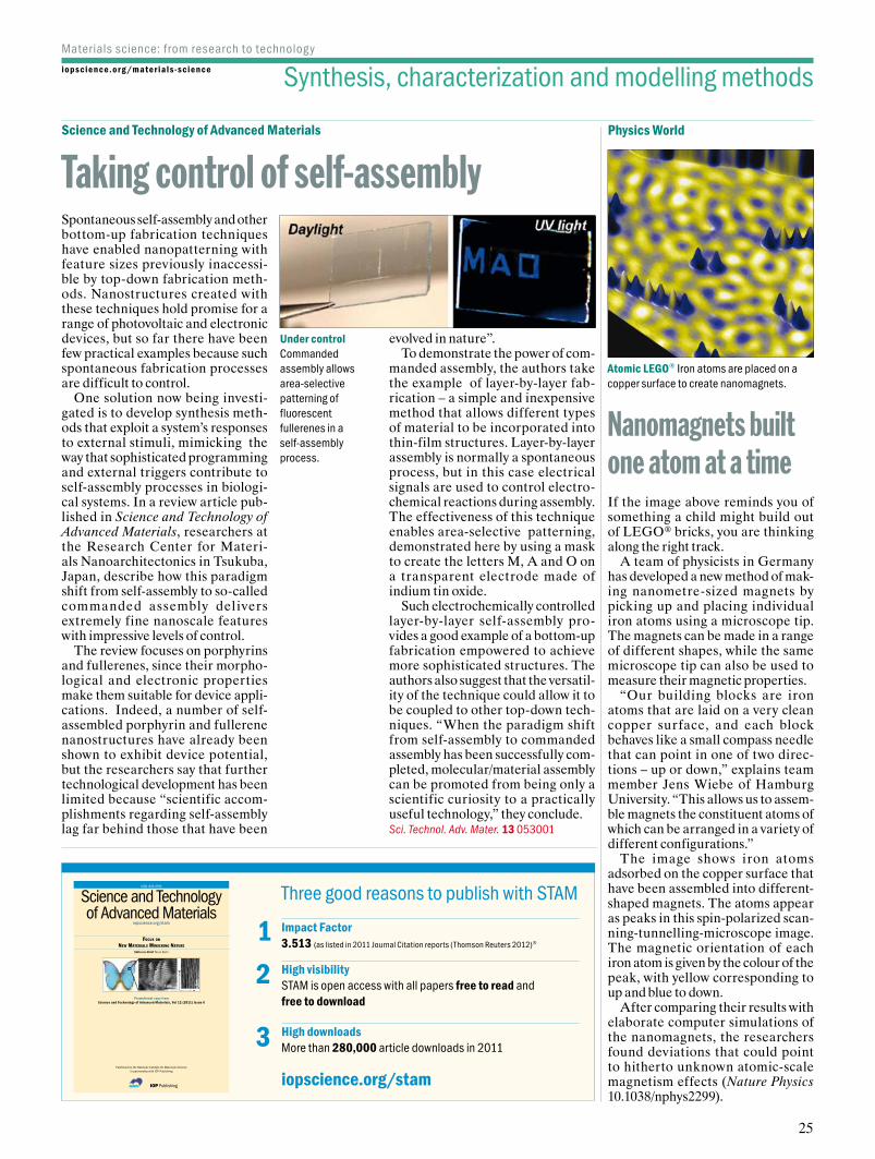
25
Synthesis, characterization and modelling methodsiopscience.org/mater ials - sc ience
Materials science: from research to technology
Spontaneous self-assembly and other bottom-up fabrication techniques have enabled nanopatterning with feature sizes previously inaccessi-ble by top-down fabrication meth-ods. Nanostructures created with these techniques hold promise for a range of photovoltaic and electronic devices, but so far there have been few practical examples because such spontaneous fabrication processes are difficult to control.
One solution now being investi-gated is to develop synthesis meth-ods that exploit a system’s responses to external stimuli, mimicking the way that sophisticated programming and external triggers contribute to self-assembly processes in biologi-cal systems. In a review article pub-lished in Science and Technology of Advanced Materials, researchers at the Research Center for Materi-als Nanoarchitectonics in Tsukuba, Japan, describe how this paradigm shift from self-assembly to so-called commanded assembly del ivers extremely fine nanoscale features with impressive levels of control.
The review focuses on porphyrins and fullerenes, since their morpho-logical and electronic properties make them suitable for device appli-cations. Indeed, a number of self-assembled porphyrin and fullerene nanostructures have already been shown to exhibit device potential, but the researchers say that further technological development has been limited because “scientific accom-plishments regarding self-assembly lag far behind those that have been
evolved in nature”.To demonstrate the power of com-
manded assembly, the authors take the example of layer-by-layer fab-rication – a simple and inexpensive method that allows different types of material to be incorporated into thin-film structures. Layer-by-layer assembly is normally a spontaneous process, but in this case electrical signals are used to control electro-chemical reactions during assembly. The effectiveness of this technique enables area-selective patterning, demonstrated here by using a mask to create the letters M, A and O on a transparent electrode made of indium tin oxide.
Such electrochemically controlled layer-by-layer self-assembly pro-vides a good example of a bottom-up fabrication empowered to achieve more sophisticated structures. The authors also suggest that the versatil-ity of the technique could allow it to be coupled to other top-down tech-niques. “When the paradigm shift from self-assembly to commanded assembly has been successfully com-pleted, molecular/material assembly can be promoted from being only a scientific curiosity to a practically useful technology,” they conclude.Sci. Technol. Adv. Mater. 13 053001
Taking control of self-assemblyScience and Technology of Advanced Materials
Under controlCommanded assembly allows area-selective patterning of fluorescent fullerenes in a self-assembly process.
If the image above reminds you of something a child might build out of LEGO® bricks, you are thinking along the right track.
A team of physicists in Germany has developed a new method of mak-ing nanometre-sized magnets by picking up and placing individual iron atoms using a microscope tip. The magnets can be made in a range of different shapes, while the same microscope tip can also be used to measure their magnetic properties.
“Our building blocks are iron atoms that are laid on a very clean copper surface, and each block behaves like a small compass needle that can point in one of two direc-tions – up or down,” explains team member Jens Wiebe of Hamburg University. “This allows us to assem-ble magnets the constituent atoms of which can be arranged in a variety of different configurations.”
The image shows iron atoms adsorbed on the copper surface that have been assembled into different-shaped magnets. The atoms appear as peaks in this spin-polarized scan-ning-tunnelling-microscope image. The magnetic orientation of each iron atom is given by the colour of the peak, with yellow corresponding to up and blue to down.
After comparing their results with elaborate computer simulations of the nanomagnets, the researchers found deviations that could point to hitherto unknown atomic-scale magnetism effects (Nature Physics 10.1038/nphys2299).
Nanomagnets built one atom at a time
Physics World
Atomic LEGO® Iron atoms are placed on a copper surface to create nanomagnets.
ISSN 1468-6996
iopscience.org/stam
Editor-in-Chief Teruo Kishi
Published by the National Institute for Materials Science in par tnership with IOP Publishing
Science and Technologyof Advanced Materials
Promotional copy fromScience and Technology of Advanced Materials, Vol 12 (2011) Issue 6
Focus on new Materials MiMicking nature
Science and Technolog
y of advanced MaTerialS
Focus articles selection December 2011
Promotional copy
Three good reasons to publish with STAM
Impact Factor 3.513 (as listed in 2011 Journal Citation reports (Thomson Reuters 2012)®
High visibility STAM is open access with all papers free to read and free to download
High downloads More than 280,000 article downloads in 2011
iopscience.org/stam
1
2
3

26
BiofabricationBiofabrication focuses on the forefront of research and development of emerging technologies that employ a range of physical, chemical, biological and engineering methods to fabricate models, systems, devices, interfaces and products oriented for bio-applications using biologically active or biologically derived materials. This research uses cells, proteins and biomaterials as building blocks to fabricate biological structures and/or cellular systems for vastly diverse applications in tissue science and engineering; in vitro biological models for 3D biology, disease pathogenesis studies and drug testing and discovery; cell/tissue/organ-on-a-chip, cell printing, patterning, and assembly and organ printing.
ISSN 1758-5082
Biofabrication
iopscience.org/bf
Featured articles:Biofabrication enables efficient interrogation and optimization of
sequential culture of endothelial cells, fibroblasts and cardiomyocytes for formation of vascular cords in cardiac tissue engineering
Rohin K iyeR, LoRaine L y Chiu, GoRdana VunjaK-noVaKoViC and MiLiCa RadisiC
An automated two-phase system for hydrogel microbead production danieLa F Coutinho, aMiR F ahaRi, nezaModdin n KaChouie,
ManueLa e GoMes, nuno M neVes, Rui L Reis and aLi KhadeMhosseini
Volume 4 Number 3 September 2012
Biofabrication Vol 4, No 3
035001–035007 Septem
ber 2012
Impact Factor
As listed in 2011 Journal Citation reports (Thomson Reuters 2012)®
3.480
Biomedical MaterialsBiomedical Materials publishes original research findings that contribute to our knowledge of the composition, properties and performance of materials for tissue engineering and regenerative medicine applications, and serves as a vehicle for the dissemination of the important work conducted internationally in this field. Topics relating to biomedical materials that are covered in this journal are: synthesis/characterization; in vitro/in vivo performance; nature-inspired synthesis/biomineralization; tissue engineering/regenerative medicine applications; interactions of cells with materials; effects of biomaterials on stem-cell behaviour, and growth factors/genes in biomaterials.
ISSN 1748-6041
BIOMEDICAL MATERIALS
Materials for t issue engineering and regenerative medicine
iopscience.org/bmm
Special Section on Materials for Healthcare Applications Symposium, EUROMAT 2011
(Montpellier, France, 12–15 September 2011)
Volume 7 Number 5 October 2012
Impact Factor
As listed in 2011 Journal Citation reports (Thomson Reuters 2012)®
2.158
Computational Science & DiscoveryComputational Science & Discovery is a multidisciplinary, international, peer- reviewed journal that aims to serve the diverse and rapidly growing computational science community by publishing work at the interface of mathematics, computation, and science application areas, including materials science and engineering. This provides authors with an opportunity to communicate computational methods and research advances across traditional disciplinary boundaries. The online format allows authors to include supplementary features such as video, audio, data, code, or other innovative presentations.
Journal of Physics: Condensed Matter
iopscience.org/jpcm
ISSN 0953-8984
Journal of PhysicsCondensed MatterJournal of Physics
w
Volume 24 Number 40 10 October 2012
Impact Factor
As listed in 2011 Journal Citation reports (Thomson Reuters 2012)®
2.546
Journal of Physics: Condensed Matter (JPCM) covers the whole of condensed matter physics including soft condensed matter and nanostructures. Papers may report experimental, theoretical or simulation studies. The area of materials science features in the journal with our published papers in this field stressing the new physics of a wide variety of materials, including materials for energy, biomaterials and advanced materials. JPCM authors benefit from fast publication times – the average receipt to online publication time for regular papers is just 70 days – and extra promotion of their most significant work.
ELECTRONIC ONLY
iopscience.org/csd
iopscience.org/bf iopscience.org/bmm
iopscience.org/jpcm
IOP materials science journals
IOP Publishing provides a range of journals covering the scope of materials science. In response to the rapid pace of research in this area we have launched an online
collection iopscience.org/materials-science to showcase the papers that we feel are at the frontiers of materials science and are making a significant contribution to this
field. The papers featured in the collection are taken from the journals listed.
iopscience.org/mater ials - sc ience
Materials science: from research to technology

27
IOP materials science journals
iopscience.org/jphysd
ISSN 0022-3727
Journal of Physics DApplied Physics
Volume 45 Number 40 10 October 2012
Topical reviewQuadrupole mass spectrometry of reactive plasmasJ Benedikt, A Hecimovic, D Ellerweg and A von Keudell
Impact Factor
As listed in 2011 Journal Citation reports (Thomson Reuters 2012)®
2.544
iopscience.org/msmse
ISSN 0965-0393
Modelling and Simulation in Materials Science and EngineeringVolume 20 Number 6 September 2012
Impact Factor
As listed in 2011 Journal Citation reports (Thomson Reuters 2012)®
2.298
NanotechnologyAny discussion of materials science would be incomplete without a reference to the extraordinary properties of nanoscale materials and their technological implications. The majority of the research published in Nanotechnology is focused on furthering our understanding of, and exploiting the properties of, nanoscale materials. With a wide range of applications from building materials and solar cells to targeted delivery of medicine and the next generation of electronic devices, nanomaterials will play a huge role in the advances of the 21st century and Nanotechnology publishes high-quality research at the leading edge of this field.
ISSN 0957-4484
NANOTECHNOLOGYVolume 23 Number 40 12 october 2012
iopscience.org/nano
Featured articleX-shaped quasi-3D plasmonic nanostructure
arrays for enhancing electric field and Raman scatteringD Wang, X Yu and Q Yu
Impact Factor
As listed in 2011 Journal Citation reports (Thomson Reuters 2012)®
3.979
ISSN 1468-6996
iopscience.org/stam
Editor-in-Chief Teruo Kishi
Published by the National Institute for Materials Science in par tnership with IOP Publishing
Science and Technologyof Advanced Materials
Promotional copy fromScience and Technology of Advanced Materials, Vol 12 (2011) Issue 6
Focus on new Materials MiMicking nature
Science and Technolog
y of advanced MaTerialS
Focus articles selection December 2011
Promotional copy
Impact Factor
As listed in 2011 Journal Citation reports (Thomson Reuters 2012)®
3.513
iopscience.org/sst
ISSN 0268-1242
Semiconductor Science and Technology
ww
Volume 27 Number 10 October 2012
Impact Factor
As listed in 2011 Journal Citation reports (Thomson Reuters 2012)®
1.723
ww
iopscience.org/sms
ISSN 0964-1726
Smart Materialsand StructuresSystems from nano- to macroscale
w
Volume 21 Number 9 September 2012
Adaptive and active materials: Selected papers from the ASME 2010 Conference on Smart Materials, Adaptive Structures and Intelligent Systems (SMASIS 11) (Scottsdale, AZ, USA, 18–21 September 2011)Guest Editors: Diann Brei, Stefan Seelecke, Nancy Johnson, Zoubeida Ounaies, Hani Naguib, John Huber, Travis Turner, Michael Philen and Vishnu Baba Sundaresan
Impact Factor
As listed in 2011 Journal Citation reports (Thomson Reuters 2012)®
2.089
Journal of Physics D: Applied PhysicsMaterials science is at the core of applied physics research and Journal of Physics D: Applied Physics (JPhysD) is proud to publish work at the forefront of this important field. The articles selected here give a flavour of the diversity of work that we publish in materials science. At JPhysD we are committed to staying one step ahead in publication speed and quality, and we would like to invite you to submit your high-quality work to the journal. With our strong Impact Factor (2.544), and our exceptionally fast decision times (average 27 days to first decision), there has never been a better time to publish with JPhysD to achieve worldwide visibility for your work.
Modelling and Simulation in Materials Science and EngineeringServing the multidisciplinary materials community, Modelling and Simulation in Materials Science and Engineering publishes new research that advances the understanding and prediction of material behaviour at scales from atomistic to macroscopic through modelling and simulation. The journal covers modelling and/or simulation that emphasizes fundamental materials issues on all classes of materials; mechanical, microstructural, electronic, chemical, biological and optical properties; multiscale materials problems; and quantitative approaches to explain and predict experimental observations.
Science and Technology of Advanced MaterialsWith an Impact Factor of 3.513, Science and Technology of Advanced Materials provides an international forum for refereed original contributions and reviews covering all aspects of materials science, including theoretical analysis, synthesis and processing, phase and structure analyses, characterization, properties, engineering and applications. This interdisciplinary journal covers advances in research on solids, liquids and colloids, and issues at the forefront of the field, such as nano-, bio- and ecomaterials. It is published in association with The National Institute for Materials Science (NIMS).
Semiconductor Science and TechnologyMaterials science has partly been driven by the development of revolutionary technologies in semiconductors among others. Articles in Semiconductor Science and Technology cover a variety of aspects from the theory, processing and characterization, to the design, manufacture and application of devices. Special issue topics published this year include atomic layer deposition and non-polar and semipolar nitride semiconductors. Looking ahead for 2013 we will be publishing issues on GaN electronics and III-V on Si devices.
Smart Materials and StructuresSmart Materials and Structures is dedicated to technical advances in smart materials, systems and structures. Since its launch in 1992, this journal has established itself as the leading publication in its field with an Impact Factor of 2.089. It is essential reading for materials scientists and engineers working on smart materials science; smart sensing and actuation (including optical sensors and wireless sensors); active control; structural health monitoring (aerospace, aviation and civil engineering); smart structures, intelligent systems and robotics; energy harvesting; smart biomimetics and bioinspiration.
iopscience.org/mater ials - sc ience
Materials science: from research to technology
iopscience.org/jphysd
iopscience.org/nano
iopscience.org/sst
iopscience.org/msmse
iopscience.org/stam
iopscience.org/sms
• National Institute for Materials Science
PARTNER

IOP materials science journals
28
Advances in Natural Science: Nanoscience and Nanotechnology
iopscience.org/ansn
Chinese Physics B
iopscience.org/cpb
Chinese Physics Letters
iopscience.org/cpl
Communications in Theoretical Physics
iopscience.org/ctp
EPL
epljournal.org
IOP Conference Series: Materials Science and Engineering
conferenceseries.iop.org
Journal of Optics
iopscience.org/jopt
Journal of Semiconductors
iopscience.org/jos
Methods and Applications in Fluorescence
iopscience.org/mafSpecial feature: Methods and Applications in Fluorescence 2012,
Guest editors david Birch, Yves MelY and otto WolfBeis
Topical review: Photoacoustic Spectroscopy for Analytical Measurements,
christoph haisch
maf.iop.org
Volume 1 Number 1 January 2000
METHODS AND APPLICATIONS IN
FLUORESCENCE
New Journal of Physics
njp.org
Physica Scripta
physica.org
Reports on Progress in Physics
iopscience.org/ropp
Superconductor Science and Technology
iopscience.org/sust
iopscience.org/mater ials - sc ience
Materials science: from research to technology
The following journals also include materials science in their scope, either as part of a broader remit or focusing on specific areas within the field:

29
PlanConsider the best way to structure your article before you start. Some journals have templates available to assist you in this process, so check this before you begin.
Choose a title that best serves your needs – an eye-catching one to attract as many readers as possible, or a descriptive one to engage readers with a specific interest in your area.
Give some thought to your abstract. It should very concisely describe the content of your paper, and encourage readers to view the entire paper. No jargon or undefined abbreviations should be used.
WritingBe clear and concise. Consider the readership of your chosen journal, bearing in mind the knowledge expected of that audience. All content of your paper should be relevant to your main scientific result.
EditingReconsider your original plan. You may decide to rewrite portions of your paper to improve clarity and conciseness.
You should repeat these processes over several successive drafts if necessary. Once the draft is ready to be submitted to a journal, carry out one final spelling and grammar check before submission.
SubmissionAll of our journals operate a fast online submission system. Simply visit the journal homepage and click on the “Submit an article” link. This will take you through to our online submission pages, where you will need to follow the steps described.
IOP Publishing supporting the materials science community
Inspired by all this great research? Here are our recommendations for successfully submitting your paper to an IOP Publishing journal.
Article Evolution is a new and ongoing project to improve the online delivery of research articles on IOPscience, enabling you to interact with research in new ways. You can enjoy a more interactive and enhanced reading experience
• It provides the functionality for you to view new articles as HTML pages
• The new article navigator contains the article contents list, the articles that users have also read, related articles and other useful links
• Tabs are attached to the left side of the article to give you instant access to reference and citation lists
• Share links next to the article title allow you to post information to a variety of social networking and bookmarking sites
• A mobile view of the article is available with improved navigation
• Video abstracts enable authors to go beyond the constraints of the written article to convey their research
• Zoom in and out of images• MathJax technology has been incorporated to improve the
rendering of mathematics • Improved export options so that you can refer back to it easily
at a later date
Article Evolution not only benefits readers, but provides a service to authors to ensure that their published work is easily accessible to the research community. Find out more at iopscience.org/article-evolution.
improving the reader experience
iopscience.org/mater ials - sc ience
Materials science: from research to technology
INTRODUCTORY GUIDE FOR AUTHORS
To help early career researchers prepare their papers for publication, we have pub-lished a digital brochure: Introductory guide for authors. The guide provides an overview of academic publishing with advice on how to choose the best outlet for your work, and to make the most of sharing your research.
The guide is available at iopscience.org/author-guide.
Introductory guide for authorsauthors.iop.org

Supporting the materials science community
30
As part of our ongoing commitment to help gain recognition for authors and their work, we regularly highlight published articles to the news media, resulting in a broad range of print, online and broadcast coverage. Here are just a few examples of materials science articles published in IOP journals that have made the headlines.
Breaking news...
HEADLINE ARTICLES
Lasers light the path to neuron regeneration In September 2011, Biofabrication published a paper that reported how lasers have been used to fabricate tiny scaffolds to be used as delivery vehicles to drop cells off at damage locations, and help treat diseases such as Alzheimer’s and Parkinson’s. This story was covered by:
• The Independent • Daily Mail • Medical News Today • phys.org V Melissinaki et al 2011 Biofabrication 3 045005
Jellyfish inspires latest ocean-powered robot Smart Materials and Structures published an article in April 2012 by American researchers who created a robotic jellyfish, named Robojelly. Not only did it have characteristics ideal to use in underwater search and rescue operations, but could, theoretically at least, never run out of energy thanks to it being fuelled by hydrogen. This story was covered by:
• BBC News • The Telegraph • Popular Mechanics • Fox News • Sydney Morning Herald • YouTube video – 244,000 views to date Yonas Tadesse et al 2012 Smart Mater. Struct. 21 045013
Handheld plasma flashlight rids skin of notorious pathogens A group of Chinese and Australian scientists published a paper in Journal of Physics D: Applied Physics in April 2012 that reported on the development of a handheld, battery-powered plasma-producing device that can rid skin of bacteria in an instant. The device could be used in ambulance emergency calls, natural disaster sites, military combat operations and many other instances where treatment is required in remote locations. This story was covered by:
• Daily Mail • The Australian • Popular Mechanics • Science magazineX Pei et al 2012 J. Phys. D: Appl. Phys. 45 165205
Methods and Applications in Fluorescence (MAF) will provide a new channel for members of the fluorescence community to discover and share research.
The journal will cover developments in fluorescence spectroscopy, imaging, fluorescent probes, labels and materials. Focusing on both methods and advanced applications, and accepting original research articles, review articles and technical notes, MAF will aim to be the natural forum for the very highest quality papers in the field.
Three Editors-in-Chief will work alongside the Editorial Board to successfully cover the broad scope of MAF:Prof. David Birch, University of Strathclyde, UK, who is also Editor-in-Chief of IOP’s journal Measurement Science & Technology.Prof. Yves Mély, University of Strasbourg, France, who is also the Chair of the “Methods and Applications of Fluorescence: Spectroscopy, Imaging & Probes” conference Permanent Steering Committee.Prof. Otto S Wolfbeis, University of Regensburg, Germany, who is also an Editor of Angewandte Chemie and founder of the “Methods and Applications of Fluorescence: Spectroscopy, Imaging & Probes” conference.
METHODS AND APPLICATIONS IN
FLUORESCENCE Special feature:
Methods and Applications in Fluorescence 2012,Guest editors david Birch, Yves MelY and otto WolfBeis
Topical review:
Photoacoustic Spectroscopy for Analytical Measurements, christoph haisch
maf.iop.org
Volume 1 Number 1 January 2000
METHODS AND APPLICATIONS IN
FLUORESCENCE
• Electronic only• Published quarterly• Open for submissions
– all published content will be freely available online until the end of 2013
Find out more atiopscience.org/maf
ISSN 1758-5082
Biofabrication
iopscience.org/bf
Featured articles:Biofabrication enables efficient interrogation and optimization of
sequential culture of endothelial cells, fibroblasts and cardiomyocytes for formation of vascular cords in cardiac tissue engineering
Rohin K iyeR, LoRaine L y Chiu, GoRdana VunjaK-noVaKoViC and MiLiCa RadisiC
An automated two-phase system for hydrogel microbead production danieLa F Coutinho, aMiR F ahaRi, nezaModdin n KaChouie,
ManueLa e GoMes, nuno M neVes, Rui L Reis and aLi KhadeMhosseini
Volume 4 Number 3 September 2012
Biofabrication Vol 4, No 3
035001–035007 Septem
ber 2012
ww
iopscience.org/sms
ISSN 0964-1726
Smart Materialsand StructuresSystems from nano- to macroscale
w
Volume 21 Number 9 September 2012
Adaptive and active materials: Selected papers from the ASME 2011 Conference on Smart Materials, Adaptive Structures and Intelligent Systems (SMASIS 11) (Scottsdale, AZ, USA, 18–21 September 2011)Guest Editors: Diann Brei, Stefan Seelecke, Nancy Johnson, Zoubeida Ounaies, Hani Naguib, John Huber, Travis Turner, Michael Philen and Vishnu Baba Sundaresan
iopscience.org/jphysd
ISSN 0022-3727
Journal of Physics DApplied Physics
Volume 45 Number 15 18 April 2012
Special issueEpitaxial grapheneGuest Editors: Walt A de Heer and Claire Berger
iopscience.org/mater ials - sc ience
Materials science: from research to technology
NEW

©2012 Thermo Fisher Scientific Inc. All rights reserved. XX52414_E 10/12M
Register for the Thermo Scientific Graphene Technical Presentations and Hands-On Workshop at
www.thermoscientific.com/mrs2012
Smarter Spectroscopy For Advanced Materials
Advanced materials offer unique properties linked to their physical forms and chemical composition. As non-destructive analytical techniques, Raman and surface analysis spectroscopy are indispensable tools for the characterization of graphene and other nanomaterials. The Thermo Scientific™ DXR Raman and the Thermo Scientific K-Alpha XPS provide rich surface, chemical, and structural information, combining research-grade performance with unmatched ease of use for exceptional productivity in materials science. Smarter spectroscopy. Definitive answers.
See what’s possible at www.thermoscientific.com/carbon
subject collections IOPBrowse the IOP subject collections for must-read research in a selection of rapidly growing fi elds.
iopscience.org/subjects

op
toelectro
nics
macro
mo
lecules
sing
le crystal silicon
diam
on
d m
icrop
ow
der
ium
Now
Inven
t.
rho
diu
m sp
on
ge
semico
nd
ucto
rs
Nd
:YAG
metam
aterials
euro
piu
m p
ho
sph
ors
green
techn
olo
gy
LED lig
htin
g
hafn
ium
tub
ing
carbo
n n
ano
tub
es titan
ium
rob
otic p
arts
99
.99
9%
ruth
eniu
m sp
heres
rare earth m
etalssp
intro
nics
go
ld n
ano
particles
ultra h
igh
pu
rity metal
germ
aniu
m w
ind
ow
serb
ium
do
ped
fiber o
ptics
yttrium
foil
silicon
carbid
e
osm
ium
nickel fo
amq
uan
tum
do
ts p
latinu
m in
k
laser crystals
bio
synth
etics
shap
e mem
ory allo
ys
alternative en
ergy
galliu
m arsen
ide
galliu
m lu
mp
battery lith
ium
catho
de
tantalu
m
aerosp
ace ultra-lig
ht allo
ysirid
ium
crucib
les
cerium
po
lishin
g p
ow
der
dysp
rosiu
m p
ellets
tantalu
m allo
ys
atom
ic layer dep
ositio
n
thin
film
stron
tium
do
ped
lanth
anu
mIII-IV
nitrid
e materials
scand
ium
-alum
inu
m
org
ano
-metallics
crystal gro
wth
anti-b
allistic ceramics
CIG
S
sup
er alloys
dielectrics
ph
oto
voltaics
ovskite
con
es
pallad
ium
sho
tsu
rface fun
ction
alized n
ano
particles
solar en
ergy
iron
liqu
ids
ano
de
cob
alt
fuel cell m
aterials
erbiu
multra
vanad
ium
bu
ckey balls
sup
ercon
du
ctors
misch
metal
targets
© 2
00
1-2
01
2. A
me
rican
Ele
me
nts is a
U.S
. Re
giste
red
Tra
de
ma
rk.
AA
NM
ER
IC
ET
SL
EM
EN
®T
he
Wo
rld’s
Ma
nu
fac
ture
r of
En
gin
ee
red
& A
dv
an
ce
d M
ate
rials
catalog: americanelem
ents.com
TM
ion
ic
Co
Ni
Cu
Zn
Ga
Ge
As
SeB
rK
rK
Ca
ScT
iV
Cr
Mn
Fe
Al
SiP
SC
lA
rN
aM
g
BC
NO
FN
eLi
Be
He
H
Rh
PdA
gC
dIn
SnSb
TeI
Xe
Rb
SrY
Zr
Nb
Mo
TcR
u
IrP
tA
uH
gT
lPb
Bi
PoA
tR
nC
sB
aLa
Hf
TaW
Re
Os
Gd
Tb
Dy
Ho
ErTm
Yb
LuC
ePr
Nd
PmSm
Eu
CmB
kC
fEs
FmM
dN
oLr
ThPa
UN
pPu
Am
Mt
Ds
Rg
Cn
Uut
Uuq
Uup
Uuh
Uus
Uuo
FrR
aA
cR
fD
bS
gB
hH
s
Untitled-1 1 19/10/2012 09:19