materials science and engineering r articles...a pt wire as the cathode). generally speaking, anodic...
TRANSCRIPT

Materials Science and Engineering R 70 (2010) 63–91
Controlled growth and modification of vertically-aligned carbon nanotubesfor multifunctional applications
Hao Chen a, Ajit Roy b, Jong-Beom Baek c, Lin Zhu d, Jia Qu a,*, Liming Dai d,*a Wenzhou Medical College, 270 Xueyuan Road, Wenzhou, Zhejiang 325027, Chinab Air Force Research Laboratory, AFRL/RX, Wright-Patterson AFB, OH 45433, USAc Interdisciplinary School of Green Energy and Institute of Advanced Materials and Chemicals, Ulsan National Institute of Science and Technology (UNIST), #100, Banyeon,
Ulsan 689-798, Republic of Koread Department of Chemical Engineering and Department of Macromolecular Science and Engineering, Case School of Engineering, Case Western Reserve University,
10900 Euclid Avenue, Cleveland, OH 44106, USA
Contents
1. Introduction . . . . . . . . . . . . . . . . . . . . . . . . . . . . . . . . . . . . . . . . . . . . . . . . . . . . . . . . . . . . . . . . . . . . . . . . . . . . . . . . . . . . . . . . . . . . . . . . . . . . . . 64
2. Controlled growth . . . . . . . . . . . . . . . . . . . . . . . . . . . . . . . . . . . . . . . . . . . . . . . . . . . . . . . . . . . . . . . . . . . . . . . . . . . . . . . . . . . . . . . . . . . . . . . . . 64
2.1. Vertically-aligned multiwalled carbon nanotubes (VA-MWNTs) . . . . . . . . . . . . . . . . . . . . . . . . . . . . . . . . . . . . . . . . . . . . . . . . . . . . . . . 64
2.1.1. VA-MWNTs by template-synthesis . . . . . . . . . . . . . . . . . . . . . . . . . . . . . . . . . . . . . . . . . . . . . . . . . . . . . . . . . . . . . . . . . . . . . . . 64
2.1.2. VA-MWNTs by template-free growth . . . . . . . . . . . . . . . . . . . . . . . . . . . . . . . . . . . . . . . . . . . . . . . . . . . . . . . . . . . . . . . . . . . . . 65
2.1.3. VA-MWNTs with special architectures . . . . . . . . . . . . . . . . . . . . . . . . . . . . . . . . . . . . . . . . . . . . . . . . . . . . . . . . . . . . . . . . . . . . 65
2.1.4. Superlong vertically-aligned carbon nanotubes (SLVA-CNTs) . . . . . . . . . . . . . . . . . . . . . . . . . . . . . . . . . . . . . . . . . . . . . . . . . . 70
2.2. Vertically-aligned single-walled carbon nanotubes (VA-SWNTs) . . . . . . . . . . . . . . . . . . . . . . . . . . . . . . . . . . . . . . . . . . . . . . . . . . . . . . . 70
2.2.1. VA-SWNTs by template-free growth . . . . . . . . . . . . . . . . . . . . . . . . . . . . . . . . . . . . . . . . . . . . . . . . . . . . . . . . . . . . . . . . . . . . . 70
2.2.2. Preferential growth of semiconducting VA-SWNTs . . . . . . . . . . . . . . . . . . . . . . . . . . . . . . . . . . . . . . . . . . . . . . . . . . . . . . . . . . 70
2.3. VA-MWNT micropatterns . . . . . . . . . . . . . . . . . . . . . . . . . . . . . . . . . . . . . . . . . . . . . . . . . . . . . . . . . . . . . . . . . . . . . . . . . . . . . . . . . . . . . . 71
2.3.1. VA-MWNT micropatterns by photolithography . . . . . . . . . . . . . . . . . . . . . . . . . . . . . . . . . . . . . . . . . . . . . . . . . . . . . . . . . . . . . 71
2.3.2. VA-MWNT micropatterns by soft-lithography . . . . . . . . . . . . . . . . . . . . . . . . . . . . . . . . . . . . . . . . . . . . . . . . . . . . . . . . . . . . . . 72
2.3.3. VA-MWNT micropatterns by plasma patterning . . . . . . . . . . . . . . . . . . . . . . . . . . . . . . . . . . . . . . . . . . . . . . . . . . . . . . . . . . . . 73
2.3.4. VA-MWNT micropatterns by e-beam lithography . . . . . . . . . . . . . . . . . . . . . . . . . . . . . . . . . . . . . . . . . . . . . . . . . . . . . . . . . . . 74
2.3.5. VA-MWNT micropatterns with 3D architectures . . . . . . . . . . . . . . . . . . . . . . . . . . . . . . . . . . . . . . . . . . . . . . . . . . . . . . . . . . . . 74
2.4. Multicomponent VA-CNT micropatterns . . . . . . . . . . . . . . . . . . . . . . . . . . . . . . . . . . . . . . . . . . . . . . . . . . . . . . . . . . . . . . . . . . . . . . . . . . 75
2.4.1. Multicomponent VA-CNT micropatterns by direct growth . . . . . . . . . . . . . . . . . . . . . . . . . . . . . . . . . . . . . . . . . . . . . . . . . . . . 76
2.4.2. Multicomponent VA-CNT micropatterns by contact transfer . . . . . . . . . . . . . . . . . . . . . . . . . . . . . . . . . . . . . . . . . . . . . . . . . . 77
3. Controlled modification . . . . . . . . . . . . . . . . . . . . . . . . . . . . . . . . . . . . . . . . . . . . . . . . . . . . . . . . . . . . . . . . . . . . . . . . . . . . . . . . . . . . . . . . . . . . . 77
3.1. Modification of VA-CNTs by plasma and photochemical activation . . . . . . . . . . . . . . . . . . . . . . . . . . . . . . . . . . . . . . . . . . . . . . . . . . . . . 77
3.2. Modification of VA-CNTs by electrochemical deposition . . . . . . . . . . . . . . . . . . . . . . . . . . . . . . . . . . . . . . . . . . . . . . . . . . . . . . . . . . . . . 79
3.3. Modification of VA-CNTs by chemical functionalization and doping . . . . . . . . . . . . . . . . . . . . . . . . . . . . . . . . . . . . . . . . . . . . . . . . . . . . 81
A R T I C L E I N F O
Article history:
Available online 1 July 2010
Keywords:
Carbon nanotube
Alignment
Patterning
Functionalization
Application
A B S T R A C T
Vertically-aligned carbon nanotubes possess many advantages for a wide range of multifunctional
applications. Along with the controlled growth of aligned/micropatterned carbon nanotubes, surface
modification of vertically-aligned carbon nanotubes are essential in order to meet specific requirements
demanded for particular applications. While many innovative synthetic methods have been developed
for controlled growth of vertically-aligned multiwalled and single-walled carbon nanotubes, various
interesting physical and chemical approaches have recently been devised for functionalization of the
constituent carbon nanotubes in vertically-aligned carbon nanotube arrays with their alignment being
largely retained. In this article, recent developments in the controlled growth and modification of
vertically-aligned carbon nanotubes for multifunctional applications are reviewed.
� 2010 Elsevier B.V. All rights reserved.
Contents lists available at ScienceDirect
Materials Science and Engineering R
journa l homepage: www.e lsev ier .com/ locate /mser
* Corresponding authors.
E-mail addresses: [email protected] (J. Qu), [email protected] (L. Dai).
0927-796X/$ – see front matter � 2010 Elsevier B.V. All rights reserved.
doi:10.1016/j.mser.2010.06.003

H. Chen et al. / Materials Science and Engineering R 70 (2010) 63–9164
3.4. Modification of VA-CNTs by polymer masking . . . . . . . . . . . . . . . . . . . . . . . . . . . . . . . . . . . . . . . . . . . . . . . . . . . . . . . . . . . . . . . . . . . . . 84
4. Concluding remarks . . . . . . . . . . . . . . . . . . . . . . . . . . . . . . . . . . . . . . . . . . . . . . . . . . . . . . . . . . . . . . . . . . . . . . . . . . . . . . . . . . . . . . . . . . . . . . . . 89
Acknowledgements . . . . . . . . . . . . . . . . . . . . . . . . . . . . . . . . . . . . . . . . . . . . . . . . . . . . . . . . . . . . . . . . . . . . . . . . . . . . . . . . . . . . . . . . . . . . . . . . 89
References . . . . . . . . . . . . . . . . . . . . . . . . . . . . . . . . . . . . . . . . . . . . . . . . . . . . . . . . . . . . . . . . . . . . . . . . . . . . . . . . . . . . . . . . . . . . . . . . . . . . . . . 89
1. Introduction
Carbon nanotubes (CNTs), including single- and multi-walledstructures, are an attractive class of nanomaterials. While a single-walled carbon nanotube (SWNT) may be conceptually viewed as agraphene sheet that is rolled into a nanoscale tube form, amultiwalled carbon nanotube (MWNT) consists of additionalgraphene coaxial tubes around the SWNT core [1,2]. SWNTs showelectric properties that are not shared by their multi-walledcounterparts. For instance, the band gap of SWNTs can vary fromzero to about 2 eV and they can exhibit metallic or semiconductingbehavior, whereas MWNTs are zero-gap metals [1,2]. This isbecause the graphene sheet in SWNTs can be rolled up withvarying degrees of twist along its length and SWNTs can have avariety of chiral structures [1–6]. Depending on their diameter andthe chirality of the orientation of graphene rings along thenanotube length, SWNTs may exhibit semiconducting or metallicbehavior. SWNTs also are more homogenous than their multi-walled counterparts, at least in terms of their diameters (�1 nm).Therefore, SWNTs are the promising candidate for micro-/nano-electronics. Apart from the semiconducting properties, character-istic of certain SWNTs, both SWNTs and MWNTs possess a highsurface area per unit weight, good mechanical properties, highelectrical conductivity at the metallic state, and high thermalconductivity/stability [1–6]. These interesting properties makeCNTs very attractive for a variety of potential applications,including as conductive materials [7–11], electromagnetic andmicrowave absorbing coatings, high-strength composites [12–14]and fibers [15–22], sensors [23,24], field emission displays [25],energy storage and energy conversion devices [26–32], radiationsources and nanometer-sized semiconductor devices [33,34], andinterconnects [33,35]. For most of the above-mentioned, and manyother applications, it is highly desirable to prepare aligned/micropatterned CNTs. Particularly, vertically-aligned CNTs (VA-CNTs) can provide a well-defined large surface area, and they canbe readily incorporated into device configurations. Besides, thealigned growth can produce CNT materials free-from amorphouscarbons with a very narrow range of tube lengths and diameters,which is an additional advantage for some of the aforementioned,and many other, applications [1,2].
On the other hand, it has also been recognized that surface and/or interfacial properties are of paramount importance for most[(Fig._1)TD$FIG]
Fig. 1. (A) High-magnification scanning electron microscope (SEM) image of carbon nano
These carbon nanotubes have diameters of �30 nm. Spacings between the nanotubes ar
surface. (B) SEM image of the mesoporous iron/silica substrate before carbon depositio
�100 nm. Many pores have relatively regular circular openings (adapted from Ref. [53
applications involving CNTs. However, it is very rare that CNTswith desirable bulk properties also possess the surface character-istics required for certain specific applications. Apart from thecontrolled growth of aligned/micropatterned CNTs, therefore,surface modification and interfacial engineering are also essentialin making functional CNT materials of good bulk and surfaceproperties as demanded for specific applications [36–42]. In thisarticle, recent developments in the controlled growth andmodification of both VA-MWNTs and VA-SWNTs are reviewed,along with discussion of their multifunctional applications.
2. Controlled growth
Carbon nanotubes synthesized by conventional techniquesusually exist in a randomly entangled form [1–6]. In view ofadditional advantages associated with VA-CNTs for many applica-tions, several chemical vapor deposition (CVD) methods have beendeveloped for large-scale production of vertically-aligned single-walled, multiwalled, and super-long carbon nanotube arrays[5,6,43–46]. These VA-CNT arrays can be transferred onto varioussubstrates of particular interest in either a patterned or non-patterned fashion. The well-aligned structure offers advantages fornot only an efficient device construction but also controlled surfacemodification. The aligned/micropatterned growth of VA-CNTs isreviewed in this section, while the modification of VA-CNTs will bediscussed in Section 3.
2.1. Vertically-aligned multiwalled carbon nanotubes (VA-MWNTs)
2.1.1. VA-MWNTs by template-synthesis
In order to construct a nanotube field emitter, de Heer et al. [47]first made an ethanol dispersion of arc-produced carbon nano-tubes. These authors then passed the nanotube dispersion throughan aluminum oxide micropore filter, leading to nanotubesperpendicularly aligned on the filter surface. The resultantperpendicularly-aligned nanotubes can be transferred onto thecathode substrate in a field emitting device. Similar porousmembranes (e.g. mesoporous silica, alumina nanoholes) have alsobeen used as a template for the so-called template-synthesis of VA-CNTs [48–52]. In particular, Li et al. [53] prepared the first largescale VA-MWNT array by CVD deposition of acetylene on ironnanoparticles embedded in mesoporpous silica at 700 8C (Fig. 1).
tubes growing out from the mesoporous iron/silica substrate and forming an array.
e �100 nm. Most of the carbon nanotubes are aligned perpendicularly on the silica
n. Pores �30 nm in diameter are distributed on the substrate and are separated by
]).

H. Chen et al. / Materials Science and Engineering R 70 (2010) 63–91 65
The growth direction of the nanotubes could be controlled by theorientation of the pores from which nanotubes grow.
Similarly, Li and Xu [48] have also reported the controlledgrowth of VA-MWNTs by the pyrolysis of hydrocarbon on a nickelcatalyst embedded in a porous silicon substrate. In these cases,porous silicons containing micro-, meso-, and macro-pores wereproduced by electrochemically etching the crystalline silicon wafer(as the anode) in an aqueous hydrofluoric acid (HF) solution (usinga Pt wire as the cathode). Generally speaking, anodic aluminumoxide films can be used for producing VA-CNTs with uniformdiameters and lengths by the pyrolysis of organic molecules intothe well-defined nanopores either with or without a catalyst[54,55].
2.1.2. VA-MWNTs by template-free growth
Without using the template pores, many groups have reportedthe growth of VA-MWNTs [2]. For instance, Rao et al. [56] haveprepared VA-MWNT arrays by high-temperature (ca. 900 8C)pyrolysis of ferrocene, which contains both metal and carbonsource required for the nanotube growth. In a separate butsomewhat related study, Kamalakaran et al. [57] reported theformation of VA-MWNT arrays by pyrolysis of a jet solution offerrocene and benzene in an argon atmosphere at relatively lowtemperatures (e.g. 850 8C). As reviewed by one of the pioneers(Meyyappan et al.) [58], plasma enhanced CVD (PECVD) has beenwidely used to produce VA-CNTs. The PECVD even allowed thegrowth of individually aligned, free-standing, vertical CNTs [58].Ren et al. [59] synthesized large arrays of VA-MWNTs by radio-frequency sputter-coating a thin nickel layer onto display glass,followed by plasma-enhanced hot filament CVD of acetylene in thepresence of ammonia gas below 666 8C. Fig. 2 shows SEM images ofthe resultant VA-MWNT arrays. These authors have also preparedVA-MWNTs on polished polycrystalline and single crystal nickelsubstrates by the plasma enhanced hot filament CVD attemperatures below 666 8C [60]. The plasma density, acetyleneto ammonia gas ratio, and gas flow rates were found to playimportant roles in regulating the diameter and uniformity of theresulting aligned CNTs. In addition to the aforementioned andsome other plasma enhanced CVD techniques [61,62], microwaveplasma enhanced CVD method has also been reported for synthesisof VA-MWNTs [63–65]. Unlike the plasma enhanced growth of VA-MWNTs, Avigal and Kalish et al. [66] reported a new method for thealigned growth by applying an electric field to a Co-coveredsubstrate in a regular cold-wall chemical vapor deposition reactor(with no plasma applied) containing flowing mixture of methaneand argon at 800 8C. They found that VA-MWNTs formed when apositive bias is applied to the substrate.
The formation of aligned carbon nanotubes from organic-metal complexes, containing both the metal catalyst and carbon
[(Fig._2)TD$FIG]Fig. 2. (A) SEM micrograph of carbon nanotubes aligned perpendicular to the substrate
length, straightness, and uniformity in height, diameter, and site density (adapted from
source required for the nanotube growth, is of particular interest,as it is a one-step process involving no pre-preparation ofcatalyst nanoparticles on the substrate used for the nanotubegrowth. In this context, Dai and co-workers [67–71] haveprepared large-scale aligned MWNTs perpendicular to thesubstrate surface by pyrolysis of iron (II) phthalocyanine,FeC32N8H16 (designated as FePc hereafter), in an Ar/H2 atmo-sphere with a dual furnace fitted with independent temperaturecontrollers. The as-synthesized nanotubes align almost normal tothe substrate surface and the constituent CNTs have a fairlyuniform tubular length and diameter with a well-graphitizedmultiwall structure [69]. Depending on whether or not thecatalytic particle is lifted up with the growing nanotube, twogrowth mechanisms, namely ‘‘tip-growth’’ and ‘‘base-growth’’,have been proposed [1,2,69]. With the FePc CVD system, wefound that the growth of carbon nanotubes start from the ironcatalyst particles, which consists of larger particles and smallerones [69]. While the smaller iron particles remaining on thesubstrate are catalytically active to support the nanotube growth,the larger iron particles are mainly responsible for producing thecarbon atomistic species from FePc vapors required for thegrowth of the nanotubes. The head-on contact between twoadjacent large iron particles in the growth front facilitates thevertical alignment [69].
With the availability of VA-MWNTs in relatively large quanti-ties, Zhang et al. [16,17] have recently produced CNT yarns andsheets from VA-MWNT forests in scalable quantities by continuoushigh-rate spinning (Fig. 3). One meter of yarn can typically be madein a few minutes. The CNT yarns and sheets are potentially usefulfor making transparent and highly conducting electrodes, planarsources of polarized broadband radiation, flexible organic light-emitting diodes, advanced sensors and actuators, microwavebonding of plastics, and thin film loudspeakers, to mention but afew applications [17,44,72]. CNT fibers have also been prepared byother methods [15,73–75].
2.1.3. VA-MWNTs with special architectures
As can be seen from the above discussion, a large variety ofsingle-component VA-CNT materials have been reported forvarious multifunctional applications [2,5,6]. Owing to their uniqueone dimensional electronic structure, CNTs offer particularadvantages as molecular wires for the development of nanotubenanodevices, including nanotube sensors and other optoelectronicsystems. There is also a pressing need to integrate multicomponentnanoscale entities into multifunctional systems and to connectthese nanosystems to the micro/macro world. Although theconnection from the nanoworld to the outside world has beenone of the long-standing problems in nanotechnology and stillremains a big challenge, a few innovative routes to the integration
over large areas. (B) Enlarged view of (A) along the peeled edge showing diameter,
Ref. [59]).

[(Fig._3)TD$FIG]
Fig. 3. SEM images showing (a) small CNT bundles simultaneously pulled and twisted from the VA-CNT forest to form CNT yarns (adapted from Ref. [16]). (b) (left) Photograph
of a transparent self-supporting MWNT sheet, and (right) SEM images showing the conversion of a VA-MWNT forest into a single MWNT sheet and a two-dimensionally
reinforced structure fabricated by overlaying four nanotube sheets with a 458 shift in orientation between successive sheets (adapted from Ref. [17]).
H. Chen et al. / Materials Science and Engineering R 70 (2010) 63–9166
of CNTs into multidimensional and multicomponent systems haverecently been devised [2].
2.1.3.1. VA-MWNT arrays with curly-entangled end-segments at the
top. Along with others, Qu et al. [76] and Zhao et al. [77] havesynthesized VA-CNT arrays with a straight aligning body and acurly-entangled end-segment at the top by a CVD process on aSiO2/Si wafer. During the pyrolytic growth of the VA-MWNTs, theinitially formed nanotube segments from the ‘‘base growth’’process grew in random directions and form a ‘‘coiled/entangled’’nanotube top layer to which the underlying straight nanotubearrays then emerged. Following earlier attempts to mimic geckofeet using microfabricated arrays of VA-CNTs [77–80], the VA-MWNT arrays produced by a low-pressure CVD process with curly-entangled end-segments at the top were demonstrated to be idealfor mimicking gecko-feet hairs [76]. In particular, Qu et al. [76]have found that the ‘‘coiled/entangled’’ nanotube top layer couldcreate an anisotropic adhesion force through the sidewall contactwith various substrates. It is believed that the difference betweennormal adhesion and shear adhesion facilitates the gecko to switchbetween attachment and detachment as it moves.
To demonstrate the adhesion performance of the VA-MWNTs, asmall piece of the VA-MWNT film (4 mm � 4 mm, Fig. 4A),
[(Fig._4)TD$FIG]Fig. 4. (A) A book of 1480 g in weight suspended from a glass surface using VA-MWNTs s
film, 4 mm � 4 mm. (B and C) SEM images of the VA-MWNT film under different magnific
onto the substrate with a preloading of 2 kg. The vertical and horizontal bars represent th
the same class, respectively. (E) Adhesion strength of VA-MWNTs with length 100 � 1
measured for more than 20 samples, while the two perpendicular blue dot lines define p
nanotubes and substrates shown in (E) are not to scale (adapted from Ref. [76]).
supported by a SiO2/Si substrate used for the nanotube growth,was finger pressed from the Si side onto a vertically positionedglass slide. The nanotubes in this film have diameters ranging from10 to 15 nm with a tube length of about 150 mm and a tube densityof�1010–1011 cm�2 (Fig. 4B and C). A book of 1480 g was held ontoa thin wire that was pre-glued on the back side of the SiO2/Sisubstrate. An overall adhesion force of 90.7 N/cm2 was calculatedfor the VA-MWNT dry adhesive film shown in Fig. 4A – which isalmost ten times that of a gecko foot. Similar adhesion behaviorswere observed for the VA-MWNT dry adhesive against othersubstrates with different flexibilities and surface characteristics,including ground glass plates, polytetrafluoroethylene (PTFE) film,rough sandpaper, and poly(ethylene terephthalate) (PET) sheet[76].
As shown in Fig. 4D, the normal adhesion force for VA-MWNTfilms with the tube length ranging from approximate 10–150 mmincreased slightly from 10 to 20 N/cm2. However, the correspond-ing shear adhesion force increased from 10 to 100 N/cm2 over thesame range of nanotube lengths. The shear adhesion force istypically several times stronger than the corresponding normaladhesion force at a constant nanotube length over about 10 mm.The high shear adhesion force of the VA-MWNT dry adhesiveensures a strong adhesion to the target surface for hanging heavy
upported on a silicon wafer. The top-right squared area shows the VA-MWNT array
ations. (D) Nanotube length-dependent adhesion force of VA-MWNT films attached
e deviations of the force and nanotube length measured for more than 20 samples of
0 mm at different pull-away directions. The red arrows represents the average forces
ossible deviations of the force measured for different samples of the same class. The

[(Fig._5)TD$FIG]
Fig. 5. (A) SEM and (B) schematic diagram for the morphological change of VA-MWNT arrays during adhesion measurements: (A) Top (a–f) and side (g–l) views of VA-MWNT
films with different length before (a–c, g–i) and after (d–f, i–l) adhesion measurements. (a, d, g, j: �5 mm; b, e, h, k: �70 mm; c, f, i, l: �150 mm). The arrows underneath the
words of ‘‘After’’ indicate the shear direction during the shear adhesion force measurements. (B) Preloading (a); attachment of the VA-MWNT array onto the glass substrate
(b); shear adhesion force stretching the nonaligned nanotubes on the substrate to form the ‘‘line’’ contact (c); normal adhesion force leading to the nonaligned nanotubes
‘‘point-by-point’’ peel-off from the substrate (d). Inset shows the structure similarity between the cross-section views of the VA-MWNTs and gecko’s aligned elastic hairs
(adapted from Ref. [76]).
H. Chen et al. / Materials Science and Engineering R 70 (2010) 63–91 67
objects along the shear direction, whilst a much weaker normaladhesion force allows the nanotube film to be readily detached inthe normal direction. The VA-MWNT arrays were repeatedlyattached and detached from the glass surface, and the supportedweight did not decrease [76]. To elucidate the angular-dependenceof the adhesion forces, Qu et al. [76] measured the pull-off force invarious pull-away directions. The decrease in the pull-off forcewith increasing pull-away angle shown in Fig. 4E indicates that theshear adhesion force is much stronger than the normal adhesionforce.
Qu et al. [76] further examined the morphology of the topsurface and cross-sectional area of the VA-MWNT films withdifferent tube lengths before and after the shear adhesionmeasurements. As expected, randomly entangled nanotube seg-ments arising from the initial stage of the ‘‘base-growth’’ processwere observed on the top surface of the as-synthesized VA-MWNTarrays (Fig. 5A(a–c)). After the shear adhesion force measurements,however, it was found that the top layer of the randomly entanglednanotube segments became horizontally aligned (Fig. 5A(d–f)). Thedegree for the shear-induced horizontal alignment increased withincreasing the aligned nanotube length (Fig. 5A(d–f)). Before thetesting, the nanotube ‘‘trunks’’ are uniformly aligned (Fig. 5A(g–i)).However, after binding on the wall, the vertically-alignednanotube ‘‘trunks’’ were tilted along the shear direction(Fig. 5A(j–l)). The significant increase in the shear adhesion forcewith increasing aligned nanotube length observed in Fig. 4D seemsto be directly related to the presence of the horizontally-alignednanotube segments on the top surface of the VA-MWNT dryadhesive films, which formed the tube-length-dependent hori-zontally-aligned structure under shear.
The SEM observations are consistent with the followingprocess. During the initial contact, the top nonaligned nanotubesegments (Fig. 5B(a)) adopted randomly-distributed ‘‘line’’ contactwith the glass substrate (Fig. 5B(b)). Upon shear adhesion forcemeasurement (Fig. 5B(c)), the applied shear force caused thenonaligned nanotube segments to align along the shear directionon the glass substrate (Fig. 5B(c)) and the vertically-alignednanotube ‘‘trunks’’ to tilt along the shear direction (Fig. 5A(j–l)),leading to a predominant aligned ‘‘line’’ contact with the glasssurface (Fig. 5A(d–f)). During the normal adhesion force measure-ments, however, the top nonaligned nanotube segments contactedwith the glass substrate were peeled from the substrate through a
‘‘point-by-point’’ detaching process (Fig. 5B(d)), requiring a muchlower force than that for pulling off the entire nanotube array(Fig. 4D). This anisotropic force distribution ensures strong bindingalong the shear direction and easy lifting in the normal direction.This finding should open many technological applications, rangingfrom new types of athletic shoes and car tires that have an unusualgrip, to creating window-clinging suits like Spider-Man’s, tosealing packages to bonding electronic and even aerospace vehicleparts in outer space where traditional polymer-based adhesiveswould be dried up and failed under the vacuum environment.
2.1.3.2. VA-MWNT arrays with Y-shaped at the top. Using branchednanochannel alumina templates, Li et al. [81] have produced Y-shaped carbon nanotubes by the pyrolysis of methane over cobalt-covered magnesium oxide (Fig. 6). In this case, these authors firstprepared the template with Y-branched nanochannels by anodiz-ing a highly pure aluminum sheet in 0.3 M oxalic acid at 10 8Cunder a constant voltage of 50 V for 15 h, which resulted in anhexagonal array of pores near the aluminum surface. Afterchemically removing the original film, a second anodization wasperformed under the same conditions, typically for 30 min. Theanodization voltage was then reduced to about 35 V. Because thepore cell diameter is proportional to the anodization voltage,reducing the voltage by a factor of 1/2 resulted in twice as manypores appearing in order to maintain the original total area of thetemplate, and nearly all the pores branched into two, smaller-diameter pores. As a consequence, the resulting template consistedof parallel Y-branched pores with stems about 90 nm in diameterand branches about 50 nm in diameter. Y-shaped CNTs havepotential applications in electronic and micro-/nano-fluidicdevices (e.g. electron interferometry) [82,83].
2.1.3.3. VA-MWNT arrays with ZnO nanoparticles at the top. 1Dheterojunction structures based on nanomaterials are of signifi-cance to both fundamental nanoscience [2,84] and potentialapplications in nanoscale systems, including various new elec-tronic and photonic nanodevices [85–88]. Consequently, consid-erable effort has been made in recent years to devise andcharacterize various heterojunctions between different low-dimensional nanomaterials [89–91]. Examples include the syn-theses of multiwalled CNT–zinc sulfide heterojunctions by acombination of ultrasonic and heat treatments [92], CNT–silicon

[(Fig._6)TD$FIG]
Fig. 6. Left: (a) SEM image of a Y-branched nanochannel template (scale bar: 1 mm). The inset shows where the Y branches start to grow. (b) Top-view SEM image of carbon
nanotubes aligned in the template after ion-milling of amorphous carbon on the surface (scale bar, 100 nm). The nanotube diameter is larger than the original pore owing to
thermal expansion of the template during growth. Top inset, stem part of the Y-junction tubes. Bottom left inset, close-up of the region between stem and branch portions still
embedded in the template. Bottom right inset, close-up of the top of the nanotube in its hexagonal cell. Right: transmission electron microscope (TEM) image of (a) the Y-
junction tube (scale bar, 50 nm) with a stem of about 90 nm and branches 50 nm in diameter. (b) Y-junction formed by using higher anodization voltages, resulting in stems of
about 100 nm and branches 60 nm in diameter (scale bar: 200 nm). (c) High-resolution TEM image of a typical Y-junction nanotube wall showing graphitic multiwall
structure (scale bar, 5 nm). Inset shows the part of the tube that was imaged (adapted from Ref. [81]).
H. Chen et al. / Materials Science and Engineering R 70 (2010) 63–9168
nanowire heterojunctions by localizing a suitable metal catalyst atthe end of a preformed nanotube or nanowire [85], and SWNT–gold nanorod heterojunctions through the selective solutiongrowth of Au nanorods on an SWNT structure [93]. Among them,CNT-based 1D heterojunctions are of particular interest because ofthe unique molecular geometry as well as excellent electronic,thermal, and mechanical properties intrinsically associated with
[(Fig._7)TD$FIG]Fig. 7. (a) Low-magnification SEM image of a vertically aligned CNT–ZnO heterojunction a
ZnO heterojunction and (e) a selected-area electron diffraction (SAED) pattern of a ZnO
CNTs [2,4,94]. However, the growth of VA-CNT heterojunctionarrays was a big challenge. Liu et al. [95] have reported thesynthesis of large-scale vertically aligned CNT–ZnO heterojunc-tions simply by water-assisted chemical vapor deposition ofcarbon on a zinc foil, which acts as both the substrate for the VA-CNT growth and zinc source for the formation of the ZnOnanostructures. Water, as a weak oxidizer, provides the oxygen
rray. (b and c) As for (a), under higher magnification. (d) TEM image of a typical CNT–
tip (adapted from Ref. [95]).

[(Fig._8)TD$FIG]
Fig. 8. Cross-sectional (A) and side-view (B) SEM images of the CNT-CFs. Scale bars for (A and B): 5 mm. (C) Amperometric responses to successive additions of 3 mM glucose
for (a) the glucose-oxidase-attached aligned CNT–CF electrode, and (b) the CF electrode after having been subjected to the same electrochemical oxidation and glucose
oxidase immobilization processes. The inset shows a plot for current increment against glucose concentration for the CNT–CF glucose sensor (adapted from Ref. [98]).
H. Chen et al. / Materials Science and Engineering R 70 (2010) 63–91 69
source for the formation of ZnO nanostructures and also enhancesCNT growth [43].
Fig. 7a shows a low-magnification SEM image of the as-synthesized CNT–ZnO sample, revealing a large-scale vertically-aligned array. Although the corresponding SEM images underhigher magnification in Fig. 7b and c show some misalignment atthe top of the nanotube array, Fig. 7b clearly shows the CNT–ZnOheterojunction with a ZnO crystal (bright spot) attached on the tipof each of the constituent VA-CNTs. Fig. 7c further reveals thatapproximately 40% of the ZnO nanoparticles are of hexagonalmorphology. The corresponding TEM image in Fig. 7d shows thatthe CNT thus prepared is multiwalled, and that the ZnOnanoparticle is intimately connected to the aligned CNT structure.Fig. 7e shows the selected-area electron diffraction (SAED) patternof the ZnO nanoparticle, which indicates that the as-prepared ZnOnanoparticle is single crystalline and can be indexed as hexagonalwurtzite ZnO [96]. The intimately connected heterojunctionsbetween the aligned CNTs and ZnO nanostructures thus preparedpossess interesting optoelectronic properties attractive for manypotential applications [95], including their use as field emitters andelectro-optic sensors and detectors.
2.1.3.4. Carbon fibers sheathed with VA-MWNT arrays. The growthof VA-CNTs around carbon-fibers provides a new class ofmultidimensional and multicomponent nanomaterials withwell-defined surface and interfacial structures attractive for awide range of potential applications. Thostenson et al. [97] werethe first to modify the surface of pitch-based carbon fiber bygrowing CNTs directly on carbon fibers. More recently, Qu et al.[98] have developed an effective approach for the preparation ofmultidimensional hybrid structures with individual microsizedcarbon fibers (CFs) sheathed by VA-MWNTs generated via
[(Fig._9)TD$FIG]
Fig. 9. (A) SEM and TEM images of SLVA-SWNT forests prepared by the water-assist grow
(c) TEM image of the super-long double-walled CNTs (adapted from Ref. [46]).
pyrolysis of FePc, and demonstrated their potential applicationsin various electrochemical systems. Fig. 8A and B shows SEMimages for CFs with a diameter of 7 mm surrounded by FePc-generated VA-MWNTs in either a patterned or nonpatternedfashion. For these hybrid CF-CNT coaxial structures, the carbonmicrofiber can be used as a microelectrode to connect thesurrounding VA-CNTs to the outside world. Consequently, theresultant microsized CFs sheathed with VA-CNTs could offer auseful platform for the development of multidimensional andmultifunctional nanomaterials and devices of practical signifi-cance. To demonstrate the potential of the CNT-sheathed CFs forbiosensing, Qu et al. [98] have attached glucose oxidase moleculesonto electrochemically-induced carboxylic groups on the CF-supported CNTs via classical carbodiimide chemistry. The glucoseoxidase-grafted VA-CNTs on the CF were then used to detectglucose in a 0.1 M phosphate buffer solution (pH 7.4) at roomtemperature by electrochemically probing hydrogen peroxidegenerated from glucose oxidation with glucose oxidase. Ampero-metric responses for the glucose oxidase-immobilized VA-CNTs onthe CF substrate and the pristine CF electrode to each successiveaddition of 3 mM glucose are shown in Fig. 8C. While there is noobvious current change with the addition of glucose for the CFelectrode (curve (b) of Fig. 8C), a stepwise increase in the currentsignal upon each successive addition of glucose was observed forits VA-CNT coated counterpart (curve (a) of Fig. 8C). The inset inFig. 8C shows the current increment with the glucose concentra-tion for the CNT–CF electrode, which shows a pseudo-linearrelationship indicating a high sensitivity and reliability. Theelectrochemical detection of glucose using the glucose oxidase-containing CNT electrode involves oxidation of hydrogen peroxidefrom glucose oxidation [98]. Given that many enzymatic reactionsare associated with the generation of hydrogen peroxide, the above
th method (adapted from Ref. [43]). (B) (a) A digital photograph, (b) SEM image, and
H. Chen et al. / Materials Science and Engineering R 70 (2010) 63–9170
methodology should be applicable to sense many other biologi-cally important substances.
2.1.4. Superlong vertically-aligned carbon nanotubes (SLVA-CNTs)
Recent advances in CVD techniques have facilitated the growthof super-long vertically aligned carbon nanotubes (SLVA-CNTs)with millimiter-order lengths (up to 10 mm). Despite somecontroversies in the role of H2O molecules [99,101] in thewater-assisted CVD reported by Hata et al. [43], several groupshave reproduced vertically-aligned super-long multiwalled (dou-ble-walled) and even single-walled CNTs, as exemplified in Fig. 9[43,46,101–103].
SLVA-CNTs offer significant advantages over their shortercounterparts for various potential applications, including multi-functional composites, sensors, and nanoelectronics [46]. Inaddition, their millimeter-order lengths provide novel opportu-nities for translating electronic, thermal, and other physicalproperties through individual nanotubes over large length scales.
2.2. Vertically-aligned single-walled carbon nanotubes (VA-SWNTs)
2.2.1. VA-SWNTs by template-free growth
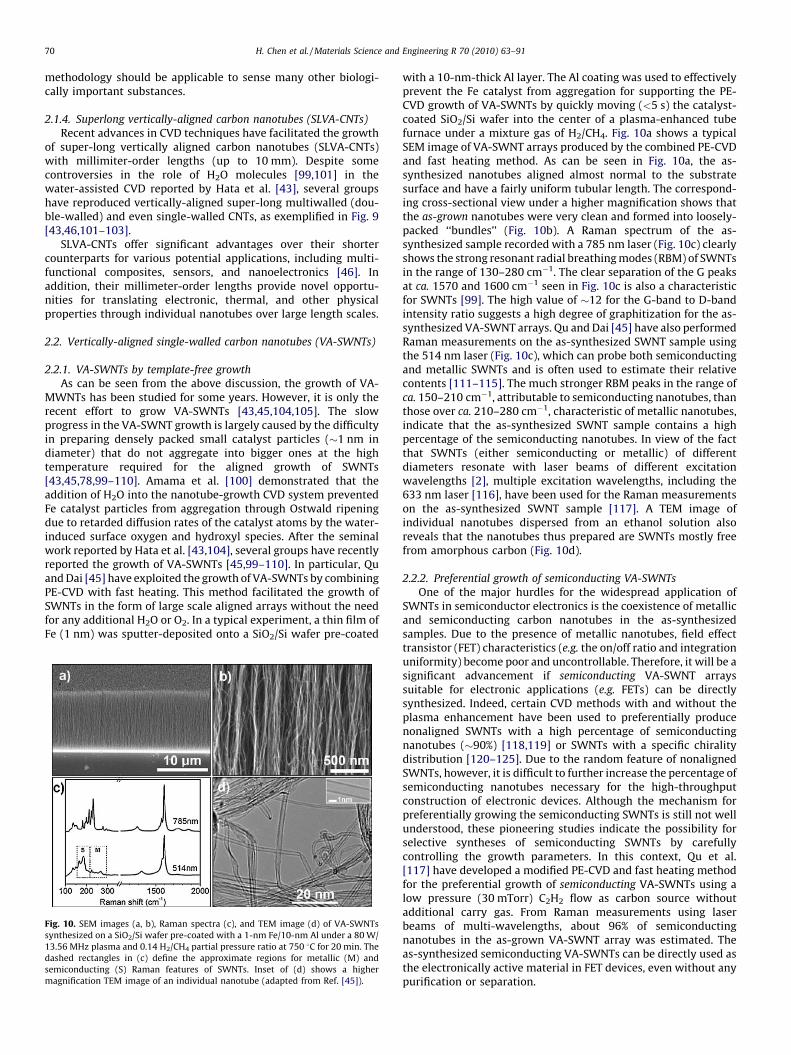
As can be seen from the above discussion, the growth of VA-MWNTs has been studied for some years. However, it is only therecent effort to grow VA-SWNTs [43,45,104,105]. The slowprogress in the VA-SWNT growth is largely caused by the difficultyin preparing densely packed small catalyst particles (�1 nm indiameter) that do not aggregate into bigger ones at the hightemperature required for the aligned growth of SWNTs[43,45,78,99–110]. Amama et al. [100] demonstrated that theaddition of H2O into the nanotube-growth CVD system preventedFe catalyst particles from aggregation through Ostwald ripeningdue to retarded diffusion rates of the catalyst atoms by the water-induced surface oxygen and hydroxyl species. After the seminalwork reported by Hata et al. [43,104], several groups have recentlyreported the growth of VA-SWNTs [45,99–110]. In particular, Quand Dai [45] have exploited the growth of VA-SWNTs by combiningPE-CVD with fast heating. This method facilitated the growth ofSWNTs in the form of large scale aligned arrays without the needfor any additional H2O or O2. In a typical experiment, a thin film ofFe (1 nm) was sputter-deposited onto a SiO2/Si wafer pre-coated
[(Fig._10)TD$FIG]Fig. 10. SEM images (a, b), Raman spectra (c), and TEM image (d) of VA-SWNTs
synthesized on a SiO2/Si wafer pre-coated with a 1-nm Fe/10-nm Al under a 80 W/
13.56 MHz plasma and 0.14 H2/CH4 partial pressure ratio at 750 8C for 20 min. The
dashed rectangles in (c) define the approximate regions for metallic (M) and
semiconducting (S) Raman features of SWNTs. Inset of (d) shows a higher
magnification TEM image of an individual nanotube (adapted from Ref. [45]).
with a 10-nm-thick Al layer. The Al coating was used to effectivelyprevent the Fe catalyst from aggregation for supporting the PE-CVD growth of VA-SWNTs by quickly moving (<5 s) the catalyst-coated SiO2/Si wafer into the center of a plasma-enhanced tubefurnace under a mixture gas of H2/CH4. Fig. 10a shows a typicalSEM image of VA-SWNT arrays produced by the combined PE-CVDand fast heating method. As can be seen in Fig. 10a, the as-synthesized nanotubes aligned almost normal to the substratesurface and have a fairly uniform tubular length. The correspond-ing cross-sectional view under a higher magnification shows thatthe as-grown nanotubes were very clean and formed into loosely-packed ‘‘bundles’’ (Fig. 10b). A Raman spectrum of the as-synthesized sample recorded with a 785 nm laser (Fig. 10c) clearlyshows the strong resonant radial breathing modes (RBM) of SWNTsin the range of 130–280 cm�1. The clear separation of the G peaksat ca. 1570 and 1600 cm�1 seen in Fig. 10c is also a characteristicfor SWNTs [99]. The high value of �12 for the G-band to D-bandintensity ratio suggests a high degree of graphitization for the as-synthesized VA-SWNT arrays. Qu and Dai [45] have also performedRaman measurements on the as-synthesized SWNT sample usingthe 514 nm laser (Fig. 10c), which can probe both semiconductingand metallic SWNTs and is often used to estimate their relativecontents [111–115]. The much stronger RBM peaks in the range ofca. 150–210 cm�1, attributable to semiconducting nanotubes, thanthose over ca. 210–280 cm�1, characteristic of metallic nanotubes,indicate that the as-synthesized SWNT sample contains a highpercentage of the semiconducting nanotubes. In view of the factthat SWNTs (either semiconducting or metallic) of differentdiameters resonate with laser beams of different excitationwavelengths [2], multiple excitation wavelengths, including the633 nm laser [116], have been used for the Raman measurementson the as-synthesized SWNT sample [117]. A TEM image ofindividual nanotubes dispersed from an ethanol solution alsoreveals that the nanotubes thus prepared are SWNTs mostly freefrom amorphous carbon (Fig. 10d).
2.2.2. Preferential growth of semiconducting VA-SWNTs
One of the major hurdles for the widespread application ofSWNTs in semiconductor electronics is the coexistence of metallicand semiconducting carbon nanotubes in the as-synthesizedsamples. Due to the presence of metallic nanotubes, field effecttransistor (FET) characteristics (e.g. the on/off ratio and integrationuniformity) become poor and uncontrollable. Therefore, it will be asignificant advancement if semiconducting VA-SWNT arrayssuitable for electronic applications (e.g. FETs) can be directlysynthesized. Indeed, certain CVD methods with and without theplasma enhancement have been used to preferentially producenonaligned SWNTs with a high percentage of semiconductingnanotubes (�90%) [118,119] or SWNTs with a specific chiralitydistribution [120–125]. Due to the random feature of nonalignedSWNTs, however, it is difficult to further increase the percentage ofsemiconducting nanotubes necessary for the high-throughputconstruction of electronic devices. Although the mechanism forpreferentially growing the semiconducting SWNTs is still not wellunderstood, these pioneering studies indicate the possibility forselective syntheses of semiconducting SWNTs by carefullycontrolling the growth parameters. In this context, Qu et al.[117] have developed a modified PE-CVD and fast heating methodfor the preferential growth of semiconducting VA-SWNTs using alow pressure (30 mTorr) C2H2 flow as carbon source withoutadditional carry gas. From Raman measurements using laserbeams of multi-wavelengths, about 96% of semiconductingnanotubes in the as-grown VA-SWNT array was estimated. Theas-synthesized semiconducting VA-SWNTs can be directly used asthe electronically active material in FET devices, even without anypurification or separation.

[(Fig._11)TD$FIG]
Fig. 11. (a) A typical SEM image of the preferentially synthesized SWNT bundle network on two electrodes; Drain current vs drain voltage measured at gate voltages ranging
from�30 to�5 V in 5 V steps for (b) the as-synthesized SWNT FET and (c) HiPco network device; and (d) drain current vs gate voltage for both the as-synthesized SWNT (&)
and HiPco (*) network devices measured at a drain voltage of 0.02 V (adapted from Ref. [117]).
H. Chen et al. / Materials Science and Engineering R 70 (2010) 63–91 71
To construct the nanotube FETs, Qu et al. [117] dispersed 0.1 mgof the as-synthesized VA-SWNTs in 1 mL DMF under ultrasonica-tion for 10 min, followed by solution-casting the slightly dispersednanotube bundles between the drain and source Au electrodes pre-fabricated on a SiO2/Si wafer (400-nm-thick SiO2) to form ananotube bundle network FET with the Si substrate as a bottomgate electrode (Fig. 11a). For comparison, these authors have alsoprepared a network FET based on HiPco SWNTs according to thesame procedure. They deliberately chose bundled nanotubesinstead of individual nanotubes for the FET investigation in orderto demonstrate the high percentage of semiconducting nanotubesin the as-grown VA-SWNT sample.
As can be seen in Fig. 11b, FETs based on SWNTs grown by thepreferential synthesis showed a typical field effect characteristicwith the drain current increasing with increasing negative gatevoltage, indicating a p-type semiconductor for the SWNTs. Incontrast, Fig. 11c shows almost no field effect for the correspondingHiPco device. The variations of drain current with the gate voltagefor a drain voltage of 0.02 V given in Fig. 11d show an on/off ratio ofmore than 100 for the as-synthesized SWNT FET in air and a quasi-linear plot with a relatively small slope for the HiPco device. Theon/off ratio of more than 100 for the as-synthesized SWNT networkFET is comparable to that of planar FETs consisting of parallelSWNTs after electrical breakdown of metallic nanotubes [126].
Due also to the similar length-scale between the nanotubelength and channel width, the presence of any metallic nanotubesin the semiconducting SWNT matrix could cause a short-circuitproblem for the FET. However, it did not happen in this case.Therefore, these results clearly indicate the high yield ofsemiconducting nanotubes in the as-synthesized VA-SWNTsample. The mobility (m) of the as-synthesized SWNTs wasestimated, according to the standard formula [127–130], to be ca.
11.4 cm2 V�1 s�1 in air, which is slightly higher than that of aplanar FET after electrical breakdown of metallic nanotube[131,132]. These preferentially-grown semiconducting VA-SWNT
arrays should be attractive for the development of variousoptoelectronic nanodevices with high performance.
2.3. VA-MWNT micropatterns
2.3.1. VA-MWNT micropatterns by photolithography
The preparation of micropatterned VA-CNTs is of paramountimportance to many potential applications related to nanotubedevices, ranging from new electron field emitters in panel displays[47], to nanotube sensor chips [132], to molecular filtrationmembranes [51]. Along with many reported approaches forfabricating micropatterns of randomly-oriented carbon nanotubes[133–136], the preparation of carbon nanotube patterns withconstituent nanotubes aligned normal to the substrate surface hasalso been discussed [5,6,25,67,68] - albeit to a less extent. Forexample, Fan et al. [25] reported the first synthesis of regulararrays of oriented nanotubes on Fe-patterned porous silicon bypyrolysis of ethylene (Fig. 12). These well-ordered nanotubes weredemonstrated to be useful as electron field emitters.
On the other hand, Yang et al. [68] developed a micropatterningmethod for photolithographic generation of the VA-MWNT arrayswith resolutions down to a micrometer scale. Fig. 13 shows the stepsof the photolithographic process (Fig. 13A), along with a typical SEMimage of the resultant VA-MWNT micropattern (Fig. 13B).
These authors first photolithographically patterned a positivephotoresist film of diazonaphthoquinone (DNQ)-modified cresolnovolak (Fig. 13C(a)) onto a quartz substrate. Upon UV irradiationthrough a photomask, the DNQ-novolak photoresist film in theexposed regions was rendered soluble in an aqueous solution ofsodium hydroxide due to photogeneration of the hydrophilicindenecarboxylic acid groups from the hydrophobic DNQ via aphotochemical Wolff rearrangement [137] (Fig. 13C(b)). They thencarried out the pyrolysis of FePc, leading to region-specific growthof the aligned carbon nanotubes in the UV exposed regions(Fig. 13B). In this case, the photolithographically patterned

[(Fig._12)TD$FIG]
Fig. 12. (Left panel) Schematic process for the synthesis of regular arrays of vertically-aligned nanotubes on porous silicon by catalyst patterning and CVD. (Right panel)
Electron micrographs of self-oriented nanotubes synthesized on n-type porous silicon substrates. (A) SEM image of nanotube blocks synthesized on 250 mm � 250 mm
catalyst patterns. The nanotubes are 80 mm long and oriented perpendicular to the substrate [see (F)]. (B) SEM image of nanotube towers synthesized on 38 mm by 38 mm
catalyst patterns. The nanotubes are 130 mm long. (C) Side view of the nanotube towers in (B). The nanotubes self-assemble such that the edges of the towers are perfectly
perpendicular to the substrate. (D) Nanotube ‘‘twin towers’’, a zoom-in view of (C). (E) SEM image showing sharp edges and corners at the top of a nanotube tower. (F) SEM
image showing that nanotubes in a block are well aligned to the direction perpendicular to the substrate surface. (G) TEM image of pure multiwalled nanotubes in several
nanotube blocks grown on a n-type porous silicon substrate. Even after ultrasonication for 15 min in 1,2-dichloroethane, the aligned and bundled configuration of the
nanotubes is still evident. The inset is a high-resolution TEM image that shows two nanotubes bundling together. The well-ordered graphitic lattice fringes of both nanotubes
are resolved (adapted from Ref. [25]).
H. Chen et al. / Materials Science and Engineering R 70 (2010) 63–9172
photoresist film, after an appropriate carbonization process, actedas a shadow mask for the patterned growth of the alignednanotubes as the polymer micropattern did not allow for the Fenanoparticle deposition due probably to a surface tensionmismatch. This method is fully compatible with existing photo-lithographic processes [138].
2.3.2. VA-MWNT micropatterns by soft-lithography
Soft-lithography has become a very promising technique formicro-/nano-structuring a wide range of materials [139–141].
[(Fig._13)TD$FIG]
Fig. 13. (A) Schematic representation of the micropattern formation of VA-MWNTs by
MWNTs prepared by the pyrolysis of FePc onto a photolithographically prepatterned qu
photochemical reactions of the DNQ-Novolak phoresist (adapted from Ref. [68]).
Various strategies, including microcontact printing (mCP), me-chanical scraping, and micromolding, have been developed fornanoscale patterning that otherwise is difficult by photolithogra-phy [142]. Using a poly(dimethylsiloxane) (PDMS) elastomerstamp, mCP has been shown to be a convenient method forgenerating self-assembled monolayer (SAM) patterns of certain‘‘molecular inks’’ (e.g. alkanethiol, alkylsiloxane) on appropriatesubstrate surfaces (e.g. gold, silver, copper, aluminum, and silicondioxide) [143–145]. Alternatively, the solvent-assisted micro-molding (SAMIM) technique allows pattern formation through
photolithographic process. (B) Typical SEM micrographs of patterned films of VA-
artz substrate. (C) (a) Molecular structure of the DNQ-Novolak photoresist, and (b)

[(Fig._14)TD$FIG]
Fig. 14. Schematic illustration of the procedure for fabricating patterns of VA-MWNTs by (a) microcontact printing, (b) solvent assisted micromolding, and (c) a typical SEM
image of a VA-MWNT micropattern prepared by the pyrolysis of FePc onto the quartz substrate prepatterned with photoresist by micromolding technique (Scale bar: 100 mm,
adapted from Ref. [70]).
H. Chen et al. / Materials Science and Engineering R 70 (2010) 63–91 73
solvent evaporation from a thin layer of polymer solution confinedbetween a PDMS elastomer mold and a substrate surface[146,147].
In addition to the photolithographic patterning describedabove, Huang et al. [70] used the micro-contact printing (mCP)and micro-molding techniques to prepare micropatterns of carbonnanotubes aligned in a direction normal to the substrate surface.While the mCP process involves the region-specific transfer of self-assembling monolayers (SAMs) of alkylsiloxane onto a quartzsubstrate and subsequent adsorption of polymer chains in theSAM-free regions (Fig. 14a), the micro-molding method [148]allows the formation of polymer patterns through solventevaporation from a precoated thin layer of polymer-solutionconfined between a quartz plate and a PDMS elastomer mold(Fig. 14b). The DNQ-Novolak photoresist patterns formed by boththe microcontact printing and solvent assisted micromolding werethen carbonized into carbon black for region-specific growth of thealigned nanotubes in the polymer-free regions (Fig. 14c) bypyrolysis of FePc under Ar/H2 atmosphere at 800–1100 8C, as is thecase for the above mentioned photolithographic patterning [68].The spatial resolution is limited by the resolution of the mask used.Micropatterns of aligned nanotubes prepared by soft-lithographyhave resolutions down to 0.8 mm [70], suitable for fabrication ofvarious electronic and photonic devices. The ease with whichmicro-/nano-patterns of organic materials can be made on curvedsurfaces by the soft-lithographic techniques [140,141] shouldprovide additional benefits to this approach with respect to thephotolithographic method, especially for the construction offlexible devices, as demonstrated in more recent studies [149–154].[(Fig._15)TD$FIG]
Fig. 15. (A) Schematic illustration of the procedure for fabricating patterns of carbon nan
plasma activation followed by region-specific adsorption of nanotubes. (B) SEM images VA
plasma-polymer-patterned quartz plate (adapted from Ref. [71]).
2.3.3. VA-MWNT micropatterns by plasma patterning
As demonstrated above, the photolithographically or soft-lithographically patterned polymer film, after an appropriatecarbonization process, can act as a shadow mask for the region-specific growth of VA-CNT micropatterns as the carbonized filmcannot support the nanotube growth while the polymer-freequartz surface allows for the growth of VA-MWNTs by pyrolysis ofFePc [68,70]. However, both the photolithographic and soft-lithographic patterning methods involve a tedious carbonizationprocess prior to the aligned nanotube growth. In order to eliminatethe carbonization process, Chen and Dai [71] have prepared carbonnanotube arrays aligned in a direction normal to the substratesurface by radio-frequency glow-discharge plasma (RFGD) poly-merization of a thin polymer pattern onto a quartz substrate(Fig. 15A), followed by region-specific growth of the VA-MWNTs inthe plasma-polymer-free regions by pyrolysis of FePc (Fig. 15B).
The highly-crosslinked structure of plasma-polymer film[155,156] should ensure the integrity of the plasma polymerlayer, even without carbonization, at high temperatures necessaryfor the nanotube growth from FePc [71] to allow the pristineplasma-polymer micropattern to act as a shadow mask for thepatterned growth of the aligned nanotubes, as is the case with thephotolithographic and soft-lithographic patterning [68,70]. There-fore, the carbonization process involved in the previous work onphotolithographic [68] and soft-lithographic [70] patterning ofthe aligned carbon nanotubes can be completely eliminated in theplasma patterning process. Owing to the generic nature of theplasma polymerization, many other organic vapors can also beused efficiently to generate plasma polymer patterns for thepatterned growth of the aligned carbon nanotubes.
otubes by (a) plasma polymerization followed by aligned nanotube growth, and (b)
-MWNT arrays growing out from the plasma-polymer-free regions on an n-hexane-

[(Fig._16)TD$FIG]
Fig. 16. (A) A series of SEM images from different viewing angles showing the growth of carbon nanotube obelisks on an array of submicron nickel dots. (a) An inclined view of
a repeated array pattern. (b) A top (normal) view of a repeated array pattern. (c) An inclined view of one array pattern. (d) A top (normal) view of one array pattern. (e) A
magnified view along the edge of one pattern. (f) An inclined view of carbon obelisks grown on nickel dots separated by 5 mm (adapted from Ref. [157]). (B) (a) Bunches of
aligned carbon nanotubes (about 100 nm) are deposited on 1 mm nickel dots by breaking up the nickel catalyst film into multiple nanoparticles. (b) Single aligned nanotubes
are deposited when the nickel dot size is reduced to 100 nm as only a single nickel nanoparticle is formed from the dot. (c) The selective growth of high yield and uniform
aligned nanotubes with different densities (adapted from Ref. [159]).
H. Chen et al. / Materials Science and Engineering R 70 (2010) 63–9174
2.3.4. VA-MWNT micropatterns by e-beam lithography
Along with the aforementioned soft-lithography, e-beamlithography has also been exploited to produce VA-CNT micro-patterns with a nanoscale resolution. For instance, Ren andco-workers [157,158] reported the growth of freestanding VA-MWNTs onto a grid of patterned submicron nickel dot(s) byplasma-enhanced hot-filament CVD using acetylene gas as thecarbon source and ammonia as the dilution gas. Individual VA-MWNTs were observed to grow well on the grid (Fig. 16A). A thinfilm nickel grid was fabricated on a silicon wafer by electron beamlithography and metal evaporation. Using this method, freestand-ing VA-MWNTs suitable for certain specific applications, such asscanning microscopy probes and electron emitters, were fabricat-ed [157,158]. Teo et al. [159] also fabricated a uniform array ofsingle, free-standing VA-MWNTs by PE-CVD on substrate pat-terned with nickel catalysts by either photolithography orelectron-beam lithography (Fig. 16B) [159].
Electron-beam deposited catalysts have also been used toproduce aligned carbon nanotubes with other controlled struc-tures [160–162]. Besides, Sohn et al. [163] have also used a similarmethod to produce aligned carbon nanotubes on Fe nanoparticlesdeposited by a pulsed laser on a porous Si substrate. These authorsfound that the growth characteristics of the carbon nanotubesdepended strongly on the Fe film deposition (by the pulse-laser)time [163].
2.3.5. VA-MWNT micropatterns with 3D architectures
Using a modified photolithographic method for patternedpyrolysis of FePc, Chen et al. [164] have prepared three-dimensional (3D) micropatterns of VA-MWNTs on the substratesurface with region-specific tubular lengths and packing densities.The photoresist system used in this approach consists of novolac/hexamethoxymethyl melamine (HMMM) as the film former,phenothiazine (RH) as the photosensitizer, and diphenyliodonium
hexafluorophosphate (Ph2I+X�) as a photoacid generator that canphotochemically generate the acid, through a photomask, requiredfor the region-specific crosslinking of the photoresist film [165].Fig. 17A represents the steps of the photolithographic process withthe associated photochemical reactions.
UV irradiation through a photo-mask creates a latent acidpattern formed by the photolithographic generation of acid fromPh2I+X� (Reaction 1 of Fig. 17B). Post-exposure baking at 110 8C for10 min caused an acid-induced crosslinking of the novolac resinand HMMM (Reactions 2 and 3 of Fig. 17B), rendering thephotoresist film in the UV-exposed regions insoluble in an aqueoussolution of sodium hydroxide (3 wt%) and ethanol (10 wt%). Incontrast, the photoresist film in the regions unexposed to the UVlight was removed simply by immersing in the developer solutionfor 10–20 s, leading to the formation of a negative polymer patternon the substrate. The crosslinking reactions between HMMM andnovolac resin were further completed by immersing the photore-sist patterned substrate into an aqueous solution of p-toluene-sulfonic acid (10 wt%) for 30 min and further baked at 150 8C for30 min [165]. The photoresist pre-patterned silica wafer or quartzplate was then directly used as the substrate for region-specificgrowing of VA-MWNTs without carbonization.
Fig. 17C represents a typical SEM image of the 3D VA-MWNTmicropatterns thus prepared, which clearly shows a region-specific packing density and tubular length. Owing to the highlycrosslinked structure between the novolac resin and HMMMwithin the photoresist patterns, the integrity of the photoresistlayer was maintained, even without the carbonization, at the hightemperatures required for the aligned nanotube growth from FePc[67]. In contrast to the DNQ-novolak photoresist film, the resultantHMMM-crosslinked novolac photoresist film supported thenanotube growth due, most probably, to its delicate surfacecharacteristics that allowed the Fe nanoparticles to deposit ontothis particular photoresist layer at the initial stage of the FePc

[(Fig._17)TD$FIG]
Fig. 17. (A) Schematic illustration of the procedures for photolithographic pattering the chemically amplified photoresist into a negative and positive pattern. (B)
photochemical reactions of the novolac/HMMM photoresistor. (C) A typical SEM micrograph of the 3D aligned carbon nanotube micropattern (adapted from Ref. [164]). (D)
Multidimensional aligned carbon nanotubes grown out from SiO2 polygons prepatterned on a Si substrate (Scale bar: 50 mm, adapted from Ref. [167]).
H. Chen et al. / Materials Science and Engineering R 70 (2010) 63–91 75
pyrolysis [67]. Different surface characteristics between the photo-exposed and non-exposed areas led to different nanotube growthrates, and hence the 3D growth. The 3D micropatterns of alignedcarbon nanotubes thus prepared offer the possibility for construc-tion of advanced microdevices with multidimensional features.
On the other hand, Ajayan and co-workers [166,167] havereported the highly substrate dependent site-selective growth ofVA-MWNTs by CVD on patterned SiO2/Si substrates usingconventional lithography. SEM results indicated that CNTs grewon the SiO2 substrate, with no observable growth on the Sisubstrate. On this basis, these authors have used photolithographyto pattern a silicon surface with silica (SiO2) polygons to allow theVA-MWNTs to grow out in several different directions at once(Fig. 17D).
[(Fig._18)TD$FIG]
Fig. 18. (A) (a) Schematic representation of photopatterning Al on a commercially-avail
micropatterns at different magnifications. (B) (a) Schematic representation of Al patt
interposed VA-SWNTs and VA-MWNTs. (b, c) Top and side view of the 3D VA-MWNT/
2.4. Multicomponent VA-CNT micropatterns
With the recent developments in nanoscience and nanotech-nology, there is a pressing need to integrate multicomponentnanoscale entities into multifunctional materials and devices. Inthis regard, Yang et al. [168] have reported a dry contact transfertechnique for preparing multicomponent carbon nanotube micro-patterns, in which COOH-containing non-aligned MWNTs wereregion-selectively adsorbed within the heptylamine-plasma-trea-ted areas interposed into the patterned structure of VA-MWNTs[71,169]. More recently, these authors have also demonstrated theformation of multicomponent carbon nanotube micropatternswith self-assembled nonaligned MWNTs interdispersed within thepatterned structure of VA-SWNTs [170]. The integration of
able iron foil for the growth of VA-SWNTs, and (b, c) SEM imgaes of the VA-SWNT
erning on a Fe-coated substrate for the patterned growth of three-dimensional,
VA-SWNT micropatterns (adapted from Ref. [45]).

H. Chen et al. / Materials Science and Engineering R 70 (2010) 63–9176
additional nanocomponent(s) into VA-CNT micropatterns thusdemonstrated could lead to novel multicomponent/multifunction-al materials and devices described below and in Section 3, thoughthe microfabrication of multicomponent VA-CNT micropatterns isstill a research field in its infancy.
2.4.1. Multicomponent VA-CNT micropatterns by direct growth
Recently, Qu and Dai [45] have found that VA-SWNTs can besynthesized on Al-activated bulk iron foil while VA-MWNTs grewwell on the Al-free iron substrate by PE-CVD of C2H2 at 750 8C.Consequently, they proceeded to grow VA-SWNT micropatterns byregion-selective coating a thin layer of Al on the bulk ironsubstrate. As shown in Fig. 18A(a), they used a photopatterningmethod to region-selectively depositing Al on a commercially-available bulk iron foil, after electropolishing, for patterned growthof VA-SWNTs. Fig. 18A(b and c) show SEM images recorded atdifferent magnifications for the VA-SWNT arrays thus prepared. Ascan be seen, VA-SWNT micropatterns having a close replication ofthe photomask structure with aligned nanotubes growing only inthe Al covered regions, suitable for microelectronic devicefabrication, are clearly evident.
Apart from the growth of VA-SWNTs on iron foils by the Alactivation described above, Qu and Dai [45] also found that thin Fe
[(Fig._19)TD$FIG]Fig. 19. (A) Schematic illustration of the procedures for fabricating multicomponent inte
specific adsorption. SEM images of (B) VA-CNT patterns after being transferred onto the Sc
dry contact transfer (i.e. negative pattern), and (D) the multicomponent interposed carbon
adsorbed between VA-CNT patterns within hexagonal regions (adapted from Ref. [168
catalyst coating (3–5 nm) on conventional substrates (e.g. SiO2/Siwafer) used for the growth of VA-MWNTs can also be activated togrow VA-SWNTs by pre-coating with a thin layer of Al. This finding,together with Al patterning, enabled them to readily preparemulticomponent micropatterns with the Al-activated VA-SWNTsinterposed within the patterned VA-MWNT arrays on an Fe pre-coated substrate (e.g. SiO2/Si wafer). Fig. 18B(a) shows the steps forpatterned deposition of an Al thin coating through a TEM grid (asthe physical mask) onto a SiO2/Si wafer pre-coated with a 3-nmthick Fe film to support the region-selective growth of VA-SWNTsover the Al covered areas and VA-MWNTs in the Al-free regions.Fig. 18B(b) shows a top view of the resultant nanotubemicropattern, in which the hexagonal windows of the TEM grid‘‘mask’’ were replicated, while the side view in Fig. 18B(c) clearlyshows the shorter VA-SWNTs interposed within the hexagonalareas surrounded by longer VA-MWNTs. The observed lengthdifference between the region-selectively-grown VA-SWNTs andVA-MWNTs resulted mainly from their different growth rates andcatalyst lifetimes. The single-walled and multiwalled nanotubecharacteristics of those shorter VA-SWNTs and longer VA-MWNTswithin the 3D multicomponet nanotube micropatterns shown inFig. 18B(b and c) were confirmed by area-selected micro-Ramanspectra (spot size �2 mm). The newly-prepared multicomponent
rposed carbon nanotube micropatterns by dry contact transfer, followed by region-
otch tape (i.e. positive pattern), (C) VA-CNT patterns left on the quartz plate after the
nanotube micropatterns with the nonaligned carbon nanotubes region-specifically
]).

H. Chen et al. / Materials Science and Engineering R 70 (2010) 63–91 77
3D VA-MWNT/VA-SWNT interposed micropatterns could serve asuseful building blocks for fabricating multifunctional micro-/nano-electronics with region-specific features while the conductingsubstrate provides a direct electrical contact.
2.4.2. Multicomponent VA-CNT micropatterns by contact transfer
Micropatterns of VA-CNTs have also been prepared by simplypressing an adhesively sticky tape (e.g. Scotch tape) prepatternedwith a nonadhesive layer onto a nonpatterned aligned nanotubefilm, followed by peeling off the sticky tape from the quartzsubstrate in a dry state [168]. Fig. 19A shows the steps used formicropatterning the Scotch tape with a thin layer of silver, thesubsequent plasma treatment of the silver surface, the contacttransfer of the aligned carbon nanotubes, and the region-specificadsorption of nonaligned carbon nanotubes. As expected, thenanotubes underneath the silver-free regions were selectivelytransferred onto the Scotch tape as a positive image of the TEM gridused as a physical mask (Fig. 19B) whereas those covered by thesilver-patterned areas remained on the quartz substrate as anegative pattern (Fig. 19C). As can be seen in Fig. 19B and C, theintegrity of those carbon nanotubes (e.g. alignment, packingdensity) transferred onto the Scotch tape is almost the same as theas-grown nanotubes remaining on the quartz plate. However, thenewly transferred carbon nanotubes with a robust aligned and/ormicropatterned structure are supported by a flexible substrate. Thecrack edges seen within the hexagonal areas in Fig. 19B were, mostprobably, caused by mechanical deformation of the silver layerwhen the overlaying flexible Scotch tape was pressed downward tothe nanotube film during the transfer process. Although some caremay be needed to prepare the aligned carbon nanotube micro-patterns with interposed crack-free silver patterns on flexibleScotch tape, the soft nature of the Scotch tape used for the drycontact transfer should allow for the development of multicom-ponent nanotube micropatterns for flexible device applications.
In conjunction with the region-specific surface modification,this dry contact transfer method has further led to the production
[(Fig._20)TD$FIG]Fig. 20. (A) Schematic representation of grafting polysaccharide chains onto plasma activa
of the Schiff-base linkage with sodium cyanoborohydride. (B) SEM images of the VA-CNTs
TEM images of an individual nanotube (a) before and (b) after being coated with a layer o
were not taken from the same spot due to technical difficulties (adapted from Ref. [18
of multicomponent carbon nanotube micropatterns in whichdifferent components are interposed in an intimate fashion[168,170]. This was exemplified by the resultant micropatternswith self-assembled nonaligned carbon nanotubes interdispersedinto the discrete areas in the patterned structure of VA-CNTs(Fig. 19D). Using different sputter-coating layers and chemistriesfor the region-specific adsorption, multicomponent micropatternsof VA-MWNTs interposed with nanoparticles or other nanomater-ials have also been produced [168,170]. The above demonstrationof the formation of multicomponent interposed VA-CNT micro-patterns by the contact-transfer micropatterning technique couldthus be very attractive for applications of carbon nanotubes invarious micro- to nano-meter scale optoelectronic devices andmany other systems.
3. Controlled modification
3.1. Modification of VA-CNTs by plasma and photochemical activation
As can be seen from the above discussion, VA-CNTs (either inpatterned or nonpatterned forms) are promising as new multi-functional materials for a variety of potential applications.However, it is very rare that VA-CNTs with desirable bulkproperties also possess the surface characteristics required forspecific applications. Along with nanoaligned CNTs, therefore,research on VA-CNTs has also been extended to include chemicalmodification. For nonaligned CNTs, the tips of CNTs have beenshown to be more reactive than their sidewalls. The treatment ofCNTs with certain acids (e.g. refluxing in HNO3 [171–174] and/orH2SO4 [175–177] was demonstrated to open the nanotube tips andto introduce –COOH and –OH groups at the opened ends [178–180]. Besides, various covalent chemistries have been developed tofunctionalize the CNT sidewalls. Examples include the covalentfluorination of CNTs within the temperature range between 250and 400 8C [181–186] or derivatization of them with certain highlyreactive chemicals such as dichlorocarbene [187,188]. Due to the
ted aligned CNTs through Schiff-base formation, followed by reductive stabilization
(a) before and (b) after the plasma polymerization of acetaldehyde. The insets show
f the acetaldehyde-plasma-polymer. Note that the micrographs shown in (a) and (b)
9]).

[(Fig._21)TD$FIG]
Fig. 21. (A) A schematic illustration of the aligned nanotube-DNA electrochemical sensor. The up-right SEM image shows the aligned CNTs after having been transferred onto
a gold foil. For reasons of clarity, only one of the many carboxyl groups is shown at the nanotube tip and wall, respectively. (B) Cyclic voltammograms of (a) the aligned carbon
nanotube electrode immobilized with ssDNA chains followed by hybridization with the FCA-labeled cDNA probes and (b) an Au electrode immobilized with ssDNA chains
followed by hybridization with the FCA-labeled cDNA probes under the same conditions. The electrochemical measurements were carried out in an aqueous solution of 0.1 M
H2SO4 vs. Ag/AgCl at a scan rate of 0.1 V s�1. The concentration of the FCA-labeled cDNA probe is 0.05 mg mL�1 (adapted from Ref. [190]).
H. Chen et al. / Materials Science and Engineering R 70 (2010) 63–9178
rather harsh conditions involved, however, most of the aboveconventional solution reactions caused the uncontrolled openingof the nanotube tips or detrimental damage to their sidewalls, orboth. Simple application of the solution chemistry to VA-CNTs canthus damage the alignment and/or the nanotube structure. Tochemically modify VA-CNTs while largely retaining their structuralintegrity, Chen et al. [189] have developed a novel approach forchemical modification of VA-CNTs by carrying out RFGD plasmatreatment, and subsequent reactions characteristic of the plasma-induced surface groups. In particular, they have reported thesurface immobilization of polysaccharide chains onto acetalde-hyde-plasma-polymer-coated VA-CNTs through the Schiff-baseformation, followed by reductive stabilization of the Schiff-baselinkage with sodium cyanoborohydride (Fig. 20). Being veryhydrophilic and biocompatible, the surface-bound polysaccharides
[(Fig._22)TD$FIG]Fig. 22. (a) SEM image of an individually addressable 3 � 3 VA-MWNT microcontact ar
samples through agarose gel) from left to right are DNA molecular-weight standard (FX
with�300 bases, and a control sample with an unrelated PCR amplicon with�400 bases,
sequence in approximately two hours. Gel electrophoresis is a DNA separation method t
matrix. The bright lights indicate the separated DNA fragments. (c) Schematic represent
array. The long single-stranded DNA PCR amplicons are hybridized to the short oligonuc
mediators are used to transfer electrons from the guanine groups to the MWNT nano
nanoelectrodes. (d) The schematic mechanism for the guanine oxidation amplified wit
provide highly hydrated coatings with important implications forusing the modified CNTs in biological systems.
The aligned nature of the VA-CNTs can not only facilitatechemical modification of VA-CNTs but also the development ofnanotube nanodevices (e.g. sensors and sensor arrays). Forinstance, He and Dai [190] have used an acetic acid plasma toactivate the VA-CNTs generated from pyrolysis of FePc[67,191,192] for grafting single-strand DNA (ssDNA) chains withan amine group at the 50-phosphate end (i.e. [AmC6]TTGACACCA-GACCAACTGGT-30) through the amide formation in the presence ofEDC coupling reagent (Fig. 21A). Complementary DNA (cDNA)chains pre-labeled with ferrocennecarboxaldehyde, FCA, (desig-nated as: [FCA-C6]ACCA-GTTGGTCTGGTGTCAA-30) were then usedfor hybridizing the surface-immobilized oligonucleotides to formdouble strand DNA (dsDNA) helices on the VA-CNT electrodes
ray (scale bar, 200 mm). (b) Gel electrophoresis. The lanes (migration lines of DNA
174RFDNAHaeIII digest), a specific polymerase chain reaction (PCR) amplicon target
respectively. PCR enables researchers to produce millions of copies of a specific DNA
hat uses electricity to separate DNA fragments by size as they migrate through a gel
ation of the mechanism to detect DNA hybridization using a MWNT nanoelectrode
leotide probes, which are functionalized at the very end of the MWNTs. Ru(bpy)32+
electrode for all target molecules within the hemispherical diffusion layer of the
h Ru(bpy)32+ mediators (adapted from Ref. [204]).

[(Fig._23)TD$FIG]
Fig. 23. (A) A free-standing film of VA-CNTs floating on the top surface of (a) a 30-azido-30-deoxythymidine solution in ethanol (2%) for UV irradiation at one side of the
nanotube film for 1 h, and (b) a perfluorooctyl iodide solution in 1,1,2,2-tetrachloroethane (2%) for UV irradiation at the opposite side of the nanotube film for 1.5 h (adapted
from Ref. [210]). (B) Plasma-oxidized VA-MWNT membrane (cross-sectional view) with carboxylic acid-derivatized MWNTs when floated on a buffer solution containing EDC
and 2-aminoethanethiol, leading to bifunctional CNTs in the membrane structure (adapted from Ref. [211]).
H. Chen et al. / Materials Science and Engineering R 70 (2010) 63–91 79
(Fig. 21A), leading to highly reversible electrochemical signalsarising from the hybridization and denaturing processes (Fig. 21B)[190]. This work demonstrated a concept for the development ofvertically-aligned CNT-DNA sensors for probing complementaryDNA chains of different base sequences with a high sensitivity andselectivity [193–195]. The ability to graft plasma-activated CNTswith DNA chains provides greater scope for not only theattachment of the additional components onto the nanotubestructure, but also the self-assembly of the modified CNTs intouseful supermolecular structures [196].
Along with the above-mentioned plasma activation and coatingof nanoscale materials [197], plasma etching [198,199] has alsobeen used to open the VA-CNT tips for membrane [200–202] andenergy-related applications [203] to be described later. Besides,Koehne and Meyyappan [204] have developed more advancedmicropatterned ultrasensitive DNA biosensors from aligned andmicropatterned CNT electrodes (Fig. 22). CNT-based flow sensorsmay also be developed for sequence-dependent separation andsensing of certain biological species, including nucleic acids[201,205,206].
The use of carbon nanotubes for many practical applicationsoften requires a precision loading of individual nanotubes intovarious functional structures and devices. The synthesis of alignedand/or micropatterned carbon nanotubes described above hasplayed a critical role in facilitating the integration of carbonnanotubes into certain useful devices (e.g. electron emitters,transistors). However, a more general self-assembling approachwould allow the construction of individual nanotubes into various
functional structures with a molecular precision. For this purpose,the site-selective chemical modification of carbon nanotubes isessential. Recent work on selective modification of carbonnanotube tips, inner walls, and/or outer walls has opened a richfield of carbon nanotube chemistry [38,39,207–209].
To achieve the asymmetric end-functionalization of carbonnanotubes with a molecular level control, Lee et al. [210] havedeveloped a simple but effective photochemical approach todirectly grafting different chemical reagents onto the oppositetube-ends of individual CNTs. This was done by sequentiallyfloating a substrate-free VA-CNT film on two different photo-reactive solutions with only one side of the VA-CNT film beingcontacted with a photoreactive solution for UV-induced functio-nalization each time, as schematically shown in Fig. 23A [210]. In asimilar but independent study, asymmetric end-functionalizationof CNTs has also been achieved through sidewall protection byimpregnating a VA-MWNT array with polystyrene [211], asschematically shown in Fig. 23B. These methodologies could beused to asymmetrically end-functionalize CNTs with ssDNA andcDNA chains onto their opposite tube-ends, which should be veryuseful for site-selective self-assembly of the asymmetrically end-functionalized CNTs into many novel functional structures.
3.2. Modification of VA-CNTs by electrochemical deposition
In addition to the plasma and photochemical activation, Gaoet al. [212] have used VA-CNTs as nanoelectrodes for makingconducting coaxial nanowires by electrochemically depositing a

[(Fig._24)TD$FIG]
Fig. 24. (A) Typical SEM images of the CP-NT coaxial nanowires produced by cyclic voltammetry on the VA-CNT electrode, showing a thin layer of conducting polymer
(polypyrrole) coating surrounding each of the constituent aligned CNTs. (B) Cyclic voltammograms of (a) the polyaniline-coated CP-NT coaxial nanowires and (b) the bare VA-
CNTs. Measured in an aqueous solution of 1 M H2SO4 with a scan rate of 50 mV/s (adapted from Ref [212]).
H. Chen et al. / Materials Science and Engineering R 70 (2010) 63–9180
concentric layer of an appropriate conducting polymer uniformlyonto each of the constituent aligned nanotubes to form thevertically-aligned conducting polymer coated CNT coaxial nano-wires (CP-NT) (Fig. 24A).
The electrochemical performance of the aligned CP-NT coaxialnanowires was evaluated by carrying out cyclic voltammetrymeasurements. As for polyaniline films electrochemically depos-ited on conventional electrodes, the cyclic voltammetric responseof the polyaniline coated nanotube array in an aqueous solution of1 M H2SO4 (Fig. 24B(a)) shows oxidation peaks at 0.33 and 0.52 V(but with much higher current densities) [213]. This indicates thatpolyaniline films thus prepared are highly electroactive. As acontrol, the cyclic voltammetry measurement was also carried outon the bare aligned nanotubes under the same conditions(Fig. 24B(b)). In the control experiment, only capacitive currentwas observed with no peak attributable to the presence of anyredoxactive species. The potential sensing applications for thevertically-aligned CP-CNT coaxial nanowires have also beendemonstrated [194]. Macroscopic coaxial carbon cylinders(�0.5 cm in diameter with varying length, �7–10 cm) consistingof VA-CNT stacks have been prepared by controlled spray pyrolysis[214]. Enhanced electrical conductivity and mechanical strengthwere observed for the resultant nanotube and polymer composites(e.g. polyethylene oxide, polyacrylamide). The coaxial structureshould allow the nanotube framework to provide a goodmechanical stability, high thermal/electrical conductivity, and
[(Fig._25)TD$FIG]
Fig. 25. (A) Procedures for the CNT innerwall modification and the asymmetric mod
nanocubes. (B) (a) SEM and (b) TEM images of CNTs having their innerwall modified w
followed by outerwall modification in an aqueous solution of K2PtCl4 containing CuCl2
configuration (adapted from Ref. [224]).
large surface/interface area necessary for efficient optoelectronicand sensing devices. The alignment structure will also allow theconstituent nanotube devices to be collectively addressed througha common substrate/electrode.
The large surface area, good chemical/mechanical stability, andexcellent electronic property also make carbon nanotubes,particularly VA-CNTs, very useful for supporting metal nanopar-ticles for many potential applications, ranging from advancedcatalytic systems, through very sensitive electrochemical sensors,to highly efficient fuel cells [215,216]. Consequently, functiona-lization of carbon nanotubes with metal nanoparticles has receivedincreasing interest in recent years, and some interesting routeshave been devised for either covalently or noncovalently attachingmetal nanoparticles onto carbon nanotubes [217–222]. Amongthem, the electroless deposition is of particular interest because itssimplicity could facilitate large-scale production of the nanotube-nanoparticle hybrids at low cost. General applications of theelectroless deposition, however, are limited by the fact that onlymetal ions of a redox potential higher than that of a reducing agentor carbon nanotube can be reduced into nanoparticles on thenanotube support. By simply supporting carbon nanotubes with ametal substrate of a redox potential lower than that of the metalions to be reduced into nanoparticles, Qu and Dai [223] haverecently developed a facile yet versatile and effective substrate-enhanced electroless deposition (SEED) method for decoratingCNTs with various metal nanoparticles, including those that cannot
ification of the nanotube innerwall with Pt nanospheres and the outerwall with
ith Pt nanospheres. (c) SEM and (d) TEM images of the innerwall-modified CNTs
with the innerwall-modified CNTs being supported by a Cu foil in a sidewall-on

H. Chen et al. / Materials Science and Engineering R 70 (2010) 63–91 81
be made by more conventional electroless deposition methods, inthe absence of any additional reducing agent [223,224]. Using thisapproach, Qu and Dai [223] have deposited Cu, Ag, Au, Pt and Pdnanoparticles onto SWNTs and MWNTs. In conjugation with VA-CNTs, asymmetric sidewall modification by attaching the inner-wall and outerwall of CNTs with metal nanoparticles of differentshapes was also achieved. As shown in Fig. 25A, VA-CNTs were firstdeposited into a commercially available alumina membrane(Fig. 25A(a)). Then Pt nanospheres were deposited onto theinnerwall of the template-synthesized VA-CNTs supported by a Cufoil (Fig. 25A(b–e)), in which the template acts as a protective layerfor the nanotube outerwall. Upon the completion of the innerwallmodification, the innerwall-modified nanotubes were released bydissolving the alumina template in aqueous HF (Fig. 25A(f)). Asexpected, Fig. 25B(a and b) shows a very smooth outerwall for theinnerwall modified CNTs. The presence of nanospheres within thenanotube innerwall was clearly seen in Fig. 25B(b). To deposit Ptnanocubes onto the outerwall, the innerwall-modified CNTs weresupported in a sidewall-on configuration (Fig. 25A(g–j)) on a Cu foiland exposed to an aqueous K2PtCl4 solution containing CuCl2 for1 min. While Fig. 25B(c) clearly shows the presence of nanocubeson the nanotube outerwall, Fig. 25B(d) reveals the asymmetricallymodified CNTs with nanocubes and nanospheres deposited ontothe nanotube outerwall and innerwall, respectively.
Using electrophoresis for titanium dioxide (TiO2) coating andphotoexicited electrons for metal nanoparticle deposition, Yanget al. [225] have also developed a facile yet versatile and effectivemethod for the development of aligned coaxial nanowires of CNTssheathed with titanium dioxide (TiO2), and well-defined TiO2
nanomembranes decorated with and without metal nanoparticles.Fig. 26a shows a typical SEM image of the VA-CNTs of ca. 7 mmlong. The corresponding SEM image under a higher magnificationin Fig. 26b shows an average diameter of ca. 50 nm for the as-synthesized CNTs. Upon electrophoresis, TiO2 clusters weredeposited on sidewalls of the VA-CNTs as nanoparticles(Fig. 26c). Further electrophoresis deposition up to approximately30 min caused additional TiO2 clusters to fill up the spacesbetween the pre-deposited TiO2 nanoparticles, leading to thegrowth of a continuous TiO2 coating along the whole nanotubelength (Fig. 26d). Fig. 26d shows similar features as the pristine VA-CNTs (Fig. 26b) but with a larger diameter (ca. 120 nm on average)due to the presence of the newly-coated TiO2 layer.
A top-view SEM image of the sample in Fig. 26d after the heattreatment at 600 8C in air for 30 min was given in Fig. 26e, whichclearly shows the vertically-aligned coaxial nanowires of CNTssheathed with TiO2 coating with some of the CNT cores havingbeen removed by oxidation with air under the high temperature.Fig. 26f shows a typical TEM image taken at the tip region of thevertically-aligned CNT-TiO2 coaxial nanowires, showing a poly-crystalline (Inset of Fig. 26f) TiO2 coating along the nanotubelength. The thickness of the TiO2 layer was determined from theTEM image to be approximately 30–40 nm, consistent with theSEM observation (cf. Fig. 26(b and d)). By annealing the samplecorresponding to Fig. 26e at 600 8C in air for 2 h, most of the VA-CNT templates were removed through air oxidation, leaving theTiO2 hollow shells as aligned TiO2 nanotubes (Fig. 26g). Prolongedelectrophoretic deposition led to partially or fully infiltrating TiO2
into the gaps between the constituent vertically-aligned CNT-TiO2
coaxial nanowires, as exemplified by Fig. 8h. Thermal annealingthe partially or fully TiO2-infiltrated VA-CNT films resulted in theformation of either a loosely-packed (Fig. 26i) or more densely-packed (Fig. 26j) TiO2 membrane. Raman spectroscopic measure-ments and XRD diffraction on the TiO2-coated VA-CNT samplecorresponding to Fig. 26e shows a TiO2 anatase phase [226].
The anatase phase of TiO2 has a band gap of approximately3.2 eV, which could be considered as a wide band gap photo-
electronically active semiconductor. Indeed, TiO2 has been widelyused as a class of photocatalysts for environment protection bydecomposing organisms with UV irradiation. Therefore, thesevertically-aligned CNT-TiO2 coaxial nanowires, TiO2 nanotubes,and TiO2 nanomembranes showed very fast photocurrentresponses to a pulsed light beam (l = 254 nm, 4 W) with a goodrepeatability (Fig. 27). The observed photocurrent responseallowed for the use of the photoexcited electrons from TiO2 todeposit various metal nanoparticles (e.g. Au, Ag, Pd, Pt) onto theTiO2 nanostructures without involving any reducing agent, as inthe case for deposition of metal nanoparticles onto CNT structuresby the aforementioned SEED method [223,224]. Similar coaxialstructures of VA-CNTs sheathed with indium tin oxide (ITO) thinfilm have also been produced by ion-assisted sputter-coating[227]. The resultant hybrid nanomaterials are expected to be usefulin solar cells, flexible electronics and displays.
3.3. Modification of VA-CNTs by chemical functionalization and
doping
The aligned CNT structure can also be well preserved via directchemical polymerization of monomer or selectively etching inliquid phase with appropriate protection. Feng et al. [228] reportedthe preparation of vertically-aligned coaxial polyaniline (PANI)-CNTs by in situ polymerization. The VA-CNTs were dipped inaniline/HCl solution, which led to the adsorption aniline monomeron the surface of CNT (Fig. 28a and b). A solution of ammoniumperoxydisulfate dissolved in HCl was added dropwise to initiatethe in situ polymerization of aniline monomer around the VA-CNTs(Fig. 28c and d). In situ polymerization by infiltrating monomermolecules into the VA-CNT arrays was also reported [229,230].
On the other hand, the aligned CNTs can also be treated by acidsolution to generate chemical functional groups at opened ends ofthe CNT. As mentioned earlier, Meyyappan and co-workers [231]developed an effective method for protecting the alignmentstructure by filling the gaps between the aligned nanotubes witha spin-on glass (SOG) prior to the oxidative reaction. Fig. 29Ashows a schematic representation of the fabrication and pretreat-ment of the aligned carbon nanotubes for further functionalization[231], whilst Fig. 29B reveals the oxidation-induced changes inalignment for the VA-CNTs with and without the SOG protection.Compared to Fig. 29B(b), Fig. 29B(c) indicates that the SOG filmprovides structural support to the aligned carbon nanotubes. Afterhaving successfully functionalized the tips of the VA-CNTs withcarboxy groups, these authors further demonstrated accomplish-ments in chemical coupling of nucleic acids to the alignednanotube array using the standard water soluble coupling reagents(i.e. EDC and N-hydroxysulfosuccinimide, sulfo-NHS), as schemat-ically shown in Fig. 29C.
Chemical doping is another approach that can be used tofunctionalize VA-CNTs at atomic scale [232–236], which intro-duces additional electronic states around the Fermi level. Thus,doped-CNTs are attractive for enhanced electron emission, chargestorage, and other nanoelectronic devices [232–238]. Gong et al.[239] have recently found that vertically aligned nitrogen-containing CNTs (VA-NCNTs) produced by pyrolysis of FePc [67],in either the presence or absence of additional NH3 vapor [240],could act as extremely effective metal-free electrocatalysts foroxygen reduction reaction (ORR) (Fig. 30). The ORR at the cathodeof fuel cells plays a key role in controlling the performance of a fuelcell, and efficient ORR electrocatalysts are essential for practicalapplications of the fuel cells [241]. The ORR at cathode, whencoupled with oxidation on the anode, produces water as the endproduct, leading to the direct conversion of chemical energy intoelectricity. Alkaline fuel cells with platinum-loaded carbon as anelectrocatalyst for the four-electron ORR were developed for the

[(Fig._26)TD$FIG]
Fig. 26. SEM images of (a) the VA-CNTs (The misalignment seen for some of the CNTs was caused by the nanotube electrode preparation), (b) as for (a) under a higher
magnification. The corresponding SEM images for the VA-CNTs after the electrophoresis deposition of TiO2 coating at 1 V at different deposition times: (c) 15 min, (d) 30 min,
and (e) top-view of the vertically-aligned CNT-TiO2 coaxial nanowires corresponding to (d) after the heat treatment at 600 8C in air for 30 min, which has been turned over
from the Si substrate to demonstrate the possibility of transferring the aligned nanowire array with full integrity. (f) A TEM image of the resultant TiO2-coated VA-CNTs shown
in (d). Inset of (f) shows an electron diffraction pattern of the TiO2 coating. SEM images of (g) the sample corresponding to (e) after thermal annealing at 600 8C in air for 2 h,
showing vertically-aligned TiO2 hollow tubes after the removal of the VA-CNT template through air oxidation, (h) VA-CNTs after a prolonged electrophoretic coating with TiO2
at 1 V for 3 h, and (i, j) the loosely and more densely packed TiO2 membranes formed by annealing the corresponding TiO2-infiltrated VA-CNT films at 600 8C in air for 2 h
(adapted from Ref. [225]).
H. Chen et al. / Materials Science and Engineering R 70 (2010) 63–9182

[(Fig._27)TD$FIG]
Fig. 27. A typical photocurrent response for a vertically-aligned CNT-TiO2 coaxial nanowire film under UV exposure (l = 254 nm, 4 W) at room temperature. Inset shows an
enlarged view for a small portion of the photocurrent response curve. The sample size is approximately 1 cm2 (adapted from Ref. [225]).
[(Fig._28)TD$FIG]
Fig. 28. Preparation procedures for coating VA-CNTs with PANI by in situ polymerization: (a) VA-MWNT film grown on a quartz substrate by catalytic pyrolysis. (b) The VA-
MWNT film was immersed into aniline/HCl solution at 0.8 8C for 12 h. (c) In situ polymerization of aniline around the MWNT surface. (d) Reaction mechanism for
polymerization of aniline around CNTs (adapted from Ref. [228]).
[(Fig._29)TD$FIG]
Fig. 29. (A) Schematic representation of the fabrication and pretreatment of the aligned carbon nanotubes for further functionalization. (B) SEM images of (a) VA-CNT arrays;
(b) the collapsed carbon nanotube array without SOG after the oxidative treatment; and (c) the aligned carbon nanotube array with SOG after the oxidative treatment. (d)
High-resolution TEM image of the opened carbon nanotube. (C) Reaction scheme for chemical coupling of nucleic acids to the VA-CNTs (adapted from Ref. [231]).
H. Chen et al. / Materials Science and Engineering R 70 (2010) 63–91 83

[(Fig._30)TD$FIG]
Fig. 30. (a) Cyclic voltammograms for the ORR at the Pt-C/GC (top) and aligned NCNT/GC (bottom) electrodes before (solid black curves) and after (dotted curves) a continuous
potentiodynamic swept for �100,000 cycles. (b) Calculated charge density distribution for the NCNTs. (c) Schematic representations of possible adsorption modes of an
oxygen molecule at the CCNTs (top) and NCNTs (bottom) (adapted from Ref. [239]).
H. Chen et al. / Materials Science and Engineering R 70 (2010) 63–9184
Apollo lunar mission in the 1960s [242], but their large-scalecommercial application has been precluded by the high cost of therequisite noble metals. Apart from its high cost, the Pt-basedelectrode also suffers from its susceptibility to time dependentdrift [243] and CO deactivation [244]. Recent research effortsfocused on reducing or replacing Pt-based electrode in fuel cellshave led to the development of new ORR electrocatalysts, includingPt-based alloys [245], carbon nanotube–supported metal particles[51,246,247], enzymatic electrocatalytic systems [248], and evenconducting poly(3,4-ethylenedioxythiophene) (PEDOT)–coatedmembranes [249]. The metal-free VA-NCNTs were shown tocatalyze a four-electron ORR process free from CO ‘‘poisoning’’with a 3-time higher electrocatalytic activity, smaller crossovereffect, and better long-term operation stability than that ofcommercially available platinum-based electrodes (C2-20, 20%platinumonVulcanXC-72R; E-TEK) in alkaline electrolytes [239]. Asteady-state output potential of �80 millivolts and a currentdensity of 4.1 milliamps per square centimeter at �0.22 volts,compared with �85 millivolts and 1.1 milliamps per squarecentimeter at �0.20 volts for a platinum-carbon electrode(Fig. 30a), have been obtained for the VA-NCNT electrode [239].
Based on the experimental observations and quantum me-chanics calculations, the improved catalytic performance for VA-NCNTs has been attributed to the electron-accepting ability of thenitrogen atoms to create net positive charge on adjacent carbonatoms in the nitrogen-doped nanotube carbon plane for facilitatingthe ORR by readily attracting electrons from the anode [239]. Thenitrogen-induced charge delocalization can also change thechemisorption mode of O2 from the usual end-on adsorption atthe CCNT surface (top, Fig. 30c) to a side-on adsorption onto theNCNT electrodes (bottom, Fig. 30c). The parallel diatomicadsorption could effectively weaken the O–O bonding to facilitateORR at the NCNT/GC electrodes. As such, doping CNTs withnitrogen heteroatoms as in the NCNT electrodes can efficientlycreate the metal-free active sites for electrochemical reduction ofO2, and even new catalytic materials for applications beyond fuelcells.
3.4. Modification of VA-CNTs by polymer masking
CNTs have been widely investigated for their application asreinforcement fillers in polymer composites [2,4,250–252]. Theability to control their interaction with and orientation withinpolymer matrices is of paramount importance for tailoring thestructure and property of the resultant nanocomposites [2,253–256]. The chemistry of CNTs has matured now for functionalizingnonaligned CNTs with various tailor-made surface characteristics
to control their interaction with polymers and other materials[36,38,208,209,257,258]. In contrast, it is just a recent develop-ment to prepare polymer and VA-CNT composites of a controllednanotube orientation in and interfacial interaction with thepolymer matrix. A few recent studies have demonstrated thatthe embedment of VA-CNTs, either partially or fully, intoappropriate polymer matrices generated important synergeticeffects that provide novel concepts and new properties formultifunctional applications, ranging from advanced chemicaland biological sensors [229,231,259–262], through smart mem-branes [200,201,263], to flexible electronics [264]. While severaldifferent matrix materials, including poly(dimethylsiloxane)(PDMS) [264], polystyrene (PS) [200,201], poly(methyl methacry-late) (PMMA) [229], spin-on-glass [231], and polydiene rubber[260], have been used for embedding VA-CNTs, solution-coatinghas remained as the main method to achieve the embedment.Although the solution-based approach provides an effective meansfor fully embedding VA-CNTs through the whole nanotube length,it could be a big challenge for the solution coating to control thenanotube length being embedded (designed as: the embedmentlength) into an appropriate matrix (e.g. polymer). By simplyheating a polymer thin film on the top of a VA-CNT array, Qu andDai [265] have demonstrated that the VA-CNTs can be embeddedinto the polymer matrix for any predetermined embedment lengthup to the whole nanotube length in a controllable fashion.
As schematically shown in Fig. 31A(a), an appropriate polymerthin film (e.g. PS; Mw = 350,000; Tg (glass transition temperature)�105 8C; Tm (melting point) �180 8C; Tc (decomposition tempera-ture) �350 8C; thickness: �50 mm) was first placed on the topsurface of a VA-CNT array (Fig. 31A(a)). Upon heating the SiO2/Sisubstrate by an underlying hot plate to a temperature above Tm
and below Tc, the melted PS film gradually filtrated into thenanotube forest (Fig. 31A(a)) through a combined effect of thegravity and capillary forces. As expected, the infiltration depth (i.e.
the embedment length) of PS into the nanotube forest dependsstrongly on the temperature and heating time. After a predeter-mined heating time, the polymer-infiltrated nanotube array waspeeled off from the SiO2/Si substrate in an aqueous solution of HF(10 wt%) to generate a free-standing film of VA-CNTs embeddedinto the PS matrix (Fig. 31A(a)). While Fig. 31A(b) shows a typicalSEM image of the pristine VA-CNTs, Fig. 31A(c–g) reproduce SEMimages of the VA-CNTs embedded into PS films after being heatedat different temperatures for 1 min. For the given infiltration timeof 1 min, the embedment length increased with the heatingtemperature from ca. 10% coverage of the nanotube length at180 8C up to the full length coverage at 245 8C (Fig. 31A(c–g)). Amore quantitative relationship between the embedment length

[(Fig._31)TD$FIG]
Fig. 31. (A) (a) Schematic representation of the VA-CNTs embeded into a polymer matrix by thermal infiltrating the melted polymer into the nanotube forest; (b–g) SEM
images of (b) the pristine VA-CNT array and (c–g) the VA-CNT array after being embedded into PS films by heating at different temperatures for 1 min. The dashed-line gaps
crossing the polymer coated regions show the approximate embedment length for each of the PS-embedded VA-CNTs; (h, i) temperature and time dependence of the
embedment length for VA-CNTs embedded into the PS matrix (L: the nanotube length (�6 mm), Ld: the embedment length, which was estimated from the distance between
the two dashed lines in each of the images shown in (c–g). (B) SEM images of individual CNTs released out from the PS-embedded VA-CNTs by THF washing after the Au
nanoparticle deposition by SEED. (a–d) correspond to samples (c–f) in (A), respectively. Scale bar: 1 mm (adapted from Ref. [265]). (C) Asymmetric functionalization of CNTs
with opposite charges. (a) A schematic representation of procedures for asymmetric functionalization of CNTs with opposite charges, followed by tube-length-specific
deposition of gold nanoparticles via electrostatical interactions; (b) a schematic representation and SEM image of the CNT array partially functionalized with cubic gold
nanoparticles; and (c) a schematic representation and SEM image of the resultant asymmetrically sidewall-functionalized CNTs with half of the nanotube length covered by
gold nanocubes and the other half by spherical gold nanoparticles through electrostatical assembly (Inset shows a higher magnification SEM image for the squared area). Scale
bars (b, c): 1 mm; Scale bar (right inset of c): 200 nm (adapted from Ref. [266]).
H. Chen et al. / Materials Science and Engineering R 70 (2010) 63–91 85
and the heating temperature is given in Fig. 31A(h), which shows apseudo-linear relationship over a wide temperature range. For agiven heating temperature (e.g. 195 8C), the embedment lengthwas found to be directly proportional to the PS filtration time (i.e.
heating time), as exemplified by Fig. 31A(i). These results clearlyshow the feasibility for the tube-length-specific functionalizationof CNTs through the controllable embedment of VA-CNTs into thepolymer matrix. This is because the portion of the nanotubesidewall embedded into the polymer matrix is physically maskedwhereas the polymer-free sidewall surface along the nanotubelength can be selectively functionalized via various physicochemi-cal processes.
In view of the ease with which shape/size-controlled metalnanoparticles can be deposited onto CNT structures by theaforementioned SEED method [223,224] and the effective actionof the deposited nanoparticles as labeling centers for characteri-zation, Qu et al. [265] have demonstrated the tube-length-specificfunctionalization of CNTs by SEED deposition of Au nanoparticles
onto each of the VA-CNTs partially embedded into the PS matricesshown in Fig. 31A(c–f) at the polymer-free region along theirsidewalls. Thereafter, the polymer support was washed off withTHF to yield individual nanotubes region-selectively attached withthe Au-nanoparticles, as shown in Fig. 31B. The portions of thenanotube length covered by the Au nanoparticles seen inFig. 31B(a–d) consist with the corresponding nanotube lengthesextending out from the polymer matrices shown in Fig. 31A(c–f),respectively. This indicates that the polymer-masking techniquecan be effectively used to precisely control the portion(s) of theCNT length to be functionalized.
The polymer-masking approach has been used not only forasymmetrically functionalizing nanotube sidewalls by sequential-ly masking VA-CNTs twice with only half of the nanotube sidewallbeing modified each time, as exemplified in Fig. 31C [266], but alsofor imparting magnetic properties to CNTs simply by region-selectively sputter-coating a thin layer of magnetic material (e.g.
iron) onto the top-tips of VA-CNTs embedded into a polymer

[(Fig._32)TD$FIG]
Fig. 32. (A) Schematic illustration for (a) fabricating and (b) characterizing the VA-CNT-polymer composite chemical vapor sensors. SEM images of the VA-MWNTs (c) before
and (d) after being partially coated with a polymer (PVAc) film on top and turned upside down (Scale bars: 5 mm). (B) DR for a vertically-aligned CNT-PVAc/PI film during (a)
cyclohexane-air and ethanol-air cycles, and (b) its equilibrium resistance peak height versus the partial cyclohexane vapor pressure (adapted from Ref. [259]).
H. Chen et al. / Materials Science and Engineering R 70 (2010) 63–9186
matrix (e.g. PS film). Therefore, this polymer-masking approach,together with those functionalization methods mentioned above,should allow for the functionalization of VA-CNTs in a region-specific fashion with various reagents (e.g. ssDNA chains of specificsequences) for developing a wide range of novel nanotube-basedmultifunctional materials and devices.
By partially coating VA-CNT arrays with an appropriatepolymer thin film along their tube length, sensors of a highsensitivity, good selectivity, and excellent environmental stabil-ity for the detection of a broad class of chemical vapors with lowpower consumption have also been developed [259]. Thediscovery of the gas sensing capabilities of nonaligned CNTsthrough the charge transfer or capacitance change by gasabsorption (e.g. NH3, NO2, O2) [142,262,267–271] is significantlyintriguing as their small size, high surface area, good environ-mental stability, and excellent mechanical and electronicproperties can offer many advantages for sensing applications[142,272,273]. However, it could be a significant advancement ifperpendicularly-aligned carbon nanotube arrays can be used asthe sensing materials because VA-CNTs, in either a patterned ornonpatterned form, allow the development of novel sensors and/or sensor chips without the need for direct manipulation ofindividual nanotubes since the constituent nanotubes can becollectively addressed through a common substrate/electrode[5,132,262]. The aligned nanotube structure further provides alarge well-defined surface area and the capacity for modifying[(Fig._33)TD$FIG]
Fig. 33. (A) Illustration of the procedure for fabricating the smart PNIPAAm/VA-CNT n
PNIPAAm/VA-CNT nanocomposite film: (b) in the dry state and (c) in the wet state. xy-
representation of the PNIPAAm/VA-MWNT film: in the dry (d) and wet (e) state at room te
(adapted from Ref. [263]).
the carbon nanotube surface with various transduction materials[5,132,262] to effectively enhance the sensitivity and to broadenthe scope of analytes to be detected. As schematically shown inFig. 32A, the absorption and desorption of chemical vapors by thepolymer matrix cause changes in the inter-tube distance, andhence the surface resistance changes across the nanotube film.Simple measurements of the resistance change, therefore,produce the sensor response. As can be seen in Fig. 32B, thechemical vapor sensors based on the aligned carbon nanotubesand poly(vinyl acetate)/polyisoprene (PVAc/PI) binary polymercomposite show reasonably good responses to both cyclohexaneand ethanol vapors (Fig. 32B(a)). The large-range good correla-tion between the equilibrium peak height for the resistancechange and the partial cyclohexane vapor pressure shown inFig. 32B(b) indicates a high sensitivity and reliability. Thevirtually unlimited number of combinations of VA-CNTs withdifferent polymer systems should make this methodology highlyversatile for developing various novel nanotube and polymersensors for effectively detecting a large variety of chemicalvapors. With appropriate surface modification for gainingspecific interactions with analytes of biological significance[39,209], these polymer-supported VA-CNT sensors could also beused to detect biological systems in solution. These flexiblecomposite films are also being developed for thermal, optical andmechanical sensors [259], and even dry adhesives mimickinggecko foot [76–80].
anocomposite films. (B) AFM images of (a) a pristine aligned CNT array and the
Scale: (a–c) 5 mm � 5 mm, z-scale: (a) 445 nm; (b) 667 nm. (c) 17 nm. A schematic
mperature (20 8C); and (f) in the wet state at a temperature above the LCST (�32 8C)
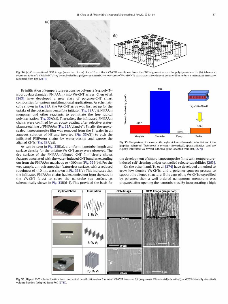
[(Fig._34)TD$FIG]
Fig. 34. (a) Cross-sectional SEM image (scale bar: 5 mm) of a �10 mm thick VA-CNT membrane. Note the CNT alignment across the polystyrene matrix. (b) Schematic
representation of a VA-MWNT array being buried in a polystyrene matrix. Hollow cores of VA-MWNTs pass across a continuous polymer film to form a membrane structure
(adapted from Ref. [211]).
[(Fig._35)TD$FIG]
Fig. 35. Comparison of measured through-thickness thermal conductivities of the
graphite adherend (facesheet), a MWNT (theoretical), epoxy adhesive, and the
expoxy-infiltrated VA-MWNT adhesive joint (adapted from Ref. [277]).
H. Chen et al. / Materials Science and Engineering R 70 (2010) 63–91 87
By infiltration of temperature responsive polymers (e.g. poly(N-isopropylacrylamide), PNIPAAm) into VA-CNT arrays, Chen et al.[263] have developed a new class of polymer-CNT smartcomposities for various multifunctional applications. As schemati-cally shown in Fig. 33A, the VA-CNT array was first set up for theuptake of the potassium persulfate initiator (Fig. 33A(a)), NIPAAmmonomer and other reactants to co-initiate the free radicalpolymerization (Fig. 33A(c)). Thereafter, the infiltrated PNIPAAmchains were confined by an epoxy coating after selective water-plasma-etching of PNIPAAm (Fig. 33A(d and e)). Finally, the epoxy-sealed nanocomposite film was removed from the Si wafer in anaqueous solution of HF and inverted (Fig. 33A(f)) to etch theinfiltrated PNIPAAm chains by water-plasma and expose thealigned CNTs (Fig. 33A(g)).
As can be seen in Fig. 33B(a), a uniform nanotube length andsurface density for the pristine VA-CNT array were observed. Thedry surface of the PNIPAAm/aligned CNT film clearly showsfeatures associated with the water-induced CNT bundles extrudingout from the PNIPAAm matrix up to�300 nm (Fig. 33B(b)). For thewet sample, a much smoother featureless surface, with a reducedroughness of�10 nm, was shown in Fig. 33B(c). This indicates thatthe infiltrated PNIPAAm chains had expanded out from the gaps inthe VA-CNT forest to cover the nanotube top surface, asschematically shown in Fig. 33B(d–f). This provided the basis for[(Fig._36)TD$FIG]
Fig. 36. Aligned CNT volume fraction from mechanical densification of ca. 1 mm tall VA-C
volume fraction (adapted from Ref. [278]).
the development of smart nanocomposite films with temperature-induced self-cleaning and/or controlled release capabilities [263].
On the other hand, Tu et al. [274] have developed a method togrow low density VA-CNTs, and a polymer-spun-on process tosupport the aligned structure. If the gaps of the VA-CNTs were filledby polymer, then a well ordered nanoporous membrane wasprepared after opening the nanotube tips. By incorporating a high
NT forests at 1% (as-grown), 8% (uniaxially densified), and 20% (biaxially densified)

H. Chen et al. / Materials Science and Engineering R 70 (2010) 63–9188
density array of VA-MWNTs through the thickness of a solidpolystyrene film and opening the nanotube end-caps at both sides(e.g. by plasma etching), Hinds and co-works [200–202] haveindeed successfully prepared VA-MWNT membranes (Fig. 34).Theses authors demonstrated that pressure driven solvent flow canpass through the VA-MWNT membrane 4 to 5 orders of magnitudefaster than a simple Newtonian fluid, illustrating the dominance ofhydrogen bond ordering. Carbon nanotube based membranes areintriguing since their pore size can be precisely controlled by thecontrolled nanotube growth and the polarity of the pore can beregion-selectively functionalized, as demonstrated by Hinds andothers [211,275,276].
Polymer-infiltrated VA-CNTs have also been used to enhancethe through-thickness thermal conductivity in the adhesivelybonded joints [277]. Fig. 35 shows the measured through-thickness thermal conductivities for a graphite facesheet(447.7 W/m K), an epoxy adhesive (0.275 W/m K), and anexpoxy-infiltrated VA-MWNT adhesive joint (250.4 W/m K). Alsoincluded in Fig. 35 is a theoretical value of the thermal conductivityfor MWNTs (2000 W/m K). As a control, the joint device withoutusing the VA-MWNTs was also measured to yield a thermalconductivity of 0.790 W/m K. Using pyrolitic graphite facesheet,
[(Fig._37)TD$FIG]Fig. 37. Fracture surfaces of VA-CNT nanocomposites. Evolution of fracture surface as vo
from Ref. [278]).
the measured through-thickness thermal conductivity for the jointconfiguration of VA-MWNTs infused with adhesive was over250 W/m K. This value of the through-thickness thermal conduc-tivity is a significant improvement compared with the one withoutthe VA-MWNTs, though still lower than that of the graphitefacesheet. Both numerical and experimental studies demonstratedthat a good thermal contact of the conductive VA-MWNTs with theadherent surfaces is essential to achieve a desirable through-thickness thermal conductivity in joints. Therefore, further workon the tip-functionalization of VA-CNTs should open avenues forthe improvement of thermal properties of structural joints andvarious opportunities for multifunctional applications related tothermal and electrical managements.
For the membrane and thermal joint, and many otherapplications, high-volume-fraction VA-CNT nanocomposites arehighly desirable. An interesting method for mechanical densifica-tion of VA-CNT forests has recently been reported by Wardle et al.[278]. The as-grown VA-MWNT volume fraction is typically 1%,giving a coverage of 109–1010 CNTs/cm2. To increase the density ofa VA-MWNT forest, these authors first released the as-grown VA-MWNT array grown on a Si substrate (1 cm2) using a standardrazor blade from the growth substrate. The released forest was
lume fraction is increased for VRM34 epoxy and VA-CNT nanocomposite (adapted

H. Chen et al. / Materials Science and Engineering R 70 (2010) 63–91 89
then placed in a small device that allowed mechanical biaxialcompression in two orthogonal directions. By varying the distancethe forest is compressed, variable-density CNT forests areobtained, as shown in Fig. 36.
The mechanical densification, in conjunction with appropriatepolymer infiltration, allowed VA-CNT nanocomposites of highvolume fractions (up to 22%) to be fabricated, as exemplified inFig. 37. Such VA-CNT nanocomposites should have potential fornumerous applications, including thermal and electrical manage-ments.
4. Concluding remarks
We have reviewed recent developments in the controlledgrowth and functionalization of VA-CNTs for multifunctionalapplications. As can be seen, a large variety of smart materials andadvanced devices could be developed from various multifunctionalVA-CNT arrays by controlled nanotube growth, in conjugation withchemical modification of the constituent CNTs. The demonstratedpotential applications of VA-CNTs and their derivatives includeelectron emitting displays, field effect transistors, chemical andbiological sensors, membranes for chemical and biologicalseparations, connectors for electrical and thermal managements,new catalysts for fuel cells, smart fibers and films for flexibleoptoelectronics, and even dry adhesives mimicking gecko foot.With so many methods available for functionalizing and control-ling nanotube growth already reported, and more to be developed,there will be vast opportunities for developing numerous newmultifunctional materials and devices from VA-CNTs.
Acknowledgements
The authors thank our colleagues, including Wei Chen, MichaelDurstock, Pinggang He, Mei Gao, Gordon Wallace, Hans Griesser,Chris Strauss, Shaoming Huang, Xiaoyin Hong, Albert Mau, QiangPeng, Liangti Qu, Morley Stone, Tia Benson-Tolle, Richard Vaia,Zhenhai Xia, Yadong Yang, Yongyong Yang, and Zhonglin Wang fortheir contributions to the work cited. We are also grateful forfinancial support from the NSF (CMS-0609077, CTS0438389, CCF-0403130), MOST of P.R. China (2009DFB30380), R&D Project ofZhejiang Province of P.R. China (2009C13019), AFOSR (FA9550-06-1-0384, FA9550-09-1-0331, FA8650-07-D-5800), AFRL, WCUProject through UNIST from the Ministry of Education, Scienceand Technology in Korea, and Wenzhou Medical College.
References
[1] P.J.F. Harris, Carbon Nanotubes and Related Structures: New Materials for theTwenty-First Century, Cambridge University Press, New York, 1999.
[2] L. Dai (Ed.), Carbon Nanotechnology: Recent Developments in Chemistry, Phys-ics, Materials Science and Device Applications, Elsevier, Amsterdam, 2006.
[3] S. Iijima, Nature 354 (1991) 56.[4] R.H. Baughman, A.A. Zakhidov, W.A. de Heer, Science 297 (2002) 787.[5] L.M. Dai, A. Patil, X.Y. Gong, Z.X. Guo, L.Q. Liu, Y. Liu, D.B. Zhu, Chem. Phys. Chem.
4 (2003) 1150, references cited therein.[6] Y. Yan, M.B. Chan-Park, Q. Zhang, Small 3 (2007) 24, reference cited therein.[7] Z.J. Fan, T. Wei, G.H. Luo, F. Wei, J. Mater. Sci. 40 (2005) 5075.[8] K. Kordas, T. Mustonen, G. Toth, H. Jantunen, M. Lajunen, C. Soldano, S. Talapatra,
S. Kar, R. Vajtai, P.M. Ajayan, Small 2 (2006) 1021.[9] W.R. Small, M.I.H. Panhuis, Small 3 (2007) 1500.
[10] T. Wei, J. Ruan, Z.J. Fan, G.H. Luo, F. Wei, Carbon 45 (2007) 2712.[11] M. Dragoman, E. Flahaut, D. Dragoman, M. Al Ahmad, R. Plana, Nanotechnology
20 (2009) 37520.[12] J.N. Coleman, U. Khan, Y.K. Gun’ko, Adv. Mater. 18 (2006) 689.[13] M. Moniruzzaman, K.I. Winey, Macromolecules 39 (2006) 5194.[14] M.J. Green, N. Behabtu, M. Pasquali, W.W. Adams, Polymer 50 (2009) 4979.[15] K.L. Jiang, Q.Q. Li, S.S. Fan, Nature 419 (2002) 801.[16] M. Zhang, K.R. Atkinson, R.H. Baughman, Science 306 (2004) 1358.[17] M. Zhang, S.L. Fang, A.A. Zakhidov, S.B. Lee, A.E. Aliev, C.D. Williams, K.R.
Atkinson, R.H. Baughman, Science 309 (2005) 1215.[18] X.B. Zhang, K.L. Jiang, C. Teng, P. Liu, L. Zhang, J. Kong, T.H. Zhang, Q.Q. Li, S.S. Fan,
Adv. Mater. 18 (2006) 1505.
[19] Q.W. Li, Y. Li, X.F. Zhang, S.B. Chikkannanavar, Y.H. Zhao, A.M. Dangelewicz, L.X.Zheng, S.K. Doorn, Q.X. Jia, D.E. Peterson, P.N. Arendt, Y.T. Zhu, Adv. Mater. 19(2007) 3358.
[20] X.F. Zhang, Q.W. Li, T.G. Holesinger, P.N. Arendt, J.Y. Huang, P.D. Kirven, T.G.Clapp, R.F. DePaula, X.Z. Liao, Y.H. Zhao, L.X. Zheng, D.E. Peterson, Y.T. Zhu, Adv.Mater. 19 (2007) 4198.
[21] K. Koziol, J. Vilatela, A. Moisala, M. Motta, P. Cunniff, M. Sennett, A. Windle,Science 318 (2007) 1892.
[22] X.F. Zhang, Q.W. Li, Y. Tu, Y.A. Li, J.Y. Coulter, L.X. Zheng, Y.H. Zhao, Q.X. Jia, D.E.Peterson, Y.T. Zhu, Small 3 (2007) 244.
[23] J.H. Liu, J.Y. Liu, L.B. Yang, X. Chen, M.Y. Zhang, F.L. Meng, T. Luo, M.Q. Li, Sensors 9(2009) 7343.
[24] K. Balasubramanian, M. Burghard, Anal. Bioanal. Chem. 385 (2006) 452.[25] S.S. Fan, M.G. Chapline, N.R. Franklin, T.W. Tombler, A.M. Cassell, H.J. Dai, Science
283 (1999) 512.[26] H. Zhang, G.P. Cao, Y.S. Yang, Energy Environ. Sci. 2 (2009) 932.[27] L.L. Zhang, X.S. Zhao, Chem. Soc. Rev. 38 (2009) 2520.[28] J. Liu, G.Z. Cao, Z.G. Yang, D.H. Wang, D. Dubois, X.D. Zhou, G.L. Graff, L.R.
Pederson, J.G. Zhang, Chem. Sus. Chem. 1 (2008) 676.[29] T. Umeyama, H. Imahori, Energy Environ. Sci. 1 (2008) 120.[30] M. Endo, M.S. Strano, P.M. Ajayan, Top. Appl. Phys. 111 (2008) 13.[31] F. Cheng, Z. Tao, J. Liang, J. Chen, Chem. Mater. 20 (2008) 667.[32] H.S. Liu, C.J. Song, L. Zhang, J.J. Zhang, H.J. Wang, D.P. Wilkinson, J. Power Sources
155 (2006) 95.[33] Q. Cao, J.A. Rogers, Adv. Mater. 21 (2009) 29.[34] P. Avouris, Z.H. Chen, V. Perebeinos, Nat. Nanotechnol. 2 (2007) 605.[35] D.C. Wei, Y.Q. Liu, Adv. Mater. 20 (2008) 2815.[36] D. Tasis, N. Tagmatarchis, V. Georgakilas, M. Prato, Chem. Eur. J. 9 (2003) 4001.[37] K.F. Fu, Y.P. Sun, J. Nanosci. Nanotechnol. 3 (2003) 351.[38] T. Lin, V. Bajpai, T. Ji, L. Dai, Aust. J. Chem. 56 (2003) 635.[39] D. Tasis, N. Tagmatarchis, A. Bianco, M. Prato, Chem. Rev. 106 (2006) 1105.[40] X.H. Peng, S.S. Wong, Adv. Mater. 21 (2009) 625.[41] P. Singh, S. Campidelli, S. Giordani, D. Bonifazi, A. Bianco, M. Prato, Chem. Soc.
Rev. 38 (2009) 2214.[42] L.J. Meng, C.L. Fu, Q.H. Lu, Prog. Nat. Sci. 19 (2009) 801.[43] K. Hata, D.N. Futaba, K. Mizuno, T. Namai, M. Yumura, S. Iijima, Science 306
(2004) 1362.[44] L. Qu, Q. Peng, L. Dai, G. Spinks, G. Wallace, R.H. Baughman, MRS Bull. 33 (2008)
215, references cited therein.[45] L. Qu, L. Dai, J. Mater. Chem. 17 (2007) 3401, references cited therein.[46] K. Gong, S. Chakrabarti, L. Dai, Angew. Chem. Int. Ed. 47 (2008) 5446.[47] W.A. de Heer, J.-M. Bonard, K. Fauth, A. Chatelain, L. Forro, D. Ugarte, Adv. Mater.
9 (1997) 87, references cited therein.[48] J. Li, C. Papadopoulos, J.M. Xu, Appl. Phys. Lett. 75 (1999) 367.[49] T. Iwasaki, T. Motoi, T. Den, Appl. Phys. Lett. 75 (1999) 2044.[50] T. Kyotani, L.F. Tsai, A. Tomita, Chem. Mater. 8 (1996) 2109.[51] G. Che, B.B. Lakshmi, E.R. Fisher, C.R. Martin, Nature 393 (1998) 346.[52] M. Terrones, N. Grobert, J. Olivares, J.P. Zhang, H. Terrones, K. Kordatos, W.K. Hsu,
P.P. Hare, P.D. Townsend, K. Prassides, A.K. Cheetham, H.W. Kroto, D.R.M.Walton, Nature 388 (1997) 52.
[53] W.Z. Li, S.S. Xie, L.X. Qian, B.H. Chang, B.S. Zou, W.Y. Zhou, R.A. Zhao, G. Wang,Science 274 (1996) 1701.
[54] T. Kyotani, B.K. Pradhan, A. Tomita, Bull. Chem. Soc. Jap. 72 (1999) 1957.[55] G. Che, B.B. Lakshmi, C.R. Martin, E.R. Fisher, R.S. Ruoff, Chem. Mater. 10 (1998)
260.[56] C.N.R. Rao, R. Sen, B.C. Satishkumar, A. Govindaraj, Chem. Commun. 1525 (1998).[57] R. Kamalakaran, M. Terrones, T. Seeger, Ph. Kohler-Redlich, M. Ruhle, Y.A. Kim, T.
Hayashi, M. Endo, Appl. Phys. Lett. 77 (2000) 21.[58] M. Meyyappan, L. Delzeit, A. Cassell, D. Hash, Plasma Sources Sci. Technol. 12
(2003) 205, references cited therein.[59] Z.F. Ren, Z.P. Huang, J.H. Xu, P.B. Wang, M.P. Siegal, P.N. Provencio, Science 282
(1998) 1105.[60] Z.P. Huang, J.W. Xu, Z.F. Ren, J.H. Wang, M.P. Siegal, P.N. Provencio, Appl. Phys.
Lett. 73 (1998) 3845.[61] H. Yasuaki, O. Takayuki, K. Masaaki, H. Hiroyuki, N. Shigehiro, ICPIG Proceedings
25th, Nagoya, Japan, July 17–22 (2001).[62] Y.H. Wang, J. Lin, C.H.A. Huan, G.S. Chen, Appl. Phys. Lett. 79 (2001) 5.[63] S.H. Tsai, C.T. Shiu, S.H. Lai, L.H. Chan, W.J. Hsieh, H.C. Shih, J. Mat. Sci. Lett. 21
(2002) 21.[64] J.Y. Lee, B.S. Lee, Thin Solid Films 418 (2002) 85.[65] B. Bower, C. Andrew, S. Jin, W. Zhu, PECVD Eur. Pat. Appl. (2001) 18.[66] Y. Avigal, R. Kalish, App. Phys. Lett. 78 (2001) 2291.[67] S.M. Huang, L. Dai, A.W.H. Mau, J. Phys. Chem. B 103 (1999) 4223.[68] Y. Yang, S. Huang, W. He, A.W.H. Mau, L. Dai, J. Am. Chem. Soc. 121 (1999) 10832.[69] D.C. Li, L. Dai, S.M. Huang, A.W.H. Mau, Z.L. Wang, Chem. Phys. Lett. 316 (2000)
349.[70] S. Huang, A.W.H. Mau, T.W. Turney, P.A. White, L. Dai, J. Phys. Chem. B 104 (2000)
2193.[71] Q. Chen, L. Dai, Appl. Phys. Lett. 76 (2000) 2719.[72] L. Xiao, Z. Chen, C. Feng, L. Liu, Z.Q. Bai, Y. Wang, L. Qian, Y.Y. Zhang, Q.Q. Li, K.L.
Jiang, S.S. Fan, Nano Lett. 8 (2008) 4539.[73] L.M. Ericson, H. Fan, H. Peng, V.A. Davis, W. Zhou, J. Sulpizio, Y. Wang, R. Booker, J.
Vavro, C. Guthy, A.N.G. Parra-Vasquez, M.J. Kim, S. Ramesh, R.K. Saini, C. Kittrell,G. Lavin, H. Schmidt, W.W. Adams, W.E. Billups, M. Pasquali, W.F. Hwang, R.H.Hauge, J.E. Fischer, R.E. Smalley, Science 305 (2004) 1447.
[74] Y. Li, I.A. Kinloch, A.H. Windle, Science 304 (2004) 274.

H. Chen et al. / Materials Science and Engineering R 70 (2010) 63–9190
[75] L. Ci, N. Punbusayakul, J. Wei, R. Vajtai, S. Talapatra, P.M. Ajayan, Adv. Mater. 19(2007) 1719.
[76] L. Qu, L. Dai, M. Stone, Z. Xia, Z.L. Wang, Science 322 (2008) 238.[77] Y. Zhao, T. Tong, L. Delzeit, A. Kashani, M. Meyyappan, A. Majumdar, J. Vac. Sci.
Technol. B 24 (2006) 331.[78] L. Qu, L. Dai, Adv. Mater. 19 (2007) 3844.[79] L. Ge, S. Sethi, L. Ci, P.M. Ajayan, A. Dhinojwala, Proc. Natl. Acad. Sci. U.S.A. 104
(2007) 10792.[80] B. Yurdumakan, N.R. Raravikar, P.M. Ajayan, A. Dhinojwala, Chem. Commun. 30
(2005) 3799.[81] C. Li, J.M. Papadopoulos, Xu, Nature 402 (1999) 253.[82] D. Grimm, P. Venezuela, F. Banhart, N. Grobert, H. Terrones, P.M. Ajayan, M.
Terrones, A. Latge, Small 3 (2007) 1900.[83] W.Z. Li, B. Pandey, Y.Q. Liu, J. Phys. Chem. B 110 (2006) 23694.[84] C. Weisbuch, B. Vinter, Quantum Semiconductor Structures: Fundamentals and
Applications, Academic, San Diego, CA, 1991.[85] J. Hu, M. Ouyang, P. Yang, C.M. Lieber, Nature 399 (1999) 48.[86] M.H. Huang, S. Mao, H. Feick, H. Yan, Y. Wu, H. Kind, E. Webber, R. Russo, P. Yang,
Science 292 (2001) 1897.[87] M.S. Gudiksen, L.J. Lauhon, J. Wang, D.C. Smith, C.M. Lieber, Nature 415 (2002)
617.[88] Y. Wu, R. Fan, P. Yang, Nano Lett. 2 (2002) 83.[89] S. Banerjee, S.S. Wong, Nano Lett. 2 (2002) 195.[90] A. Jensen, J.R. Hauptmann, J. Nygard, J. Sadowski, P.E. Lindelof, Nano Lett. 4
(2004) 349.[91] H. Kim, W. Sigmund, Appl. Phys. Lett. 81 (2002) 2085.[92] J. Du, L. Fu, Z. Liu, B. Han, Z. Li, Y. Liu, Z. Sun, D. Zhu, J. Phys. Chem. B 109 (12)
(2005) 772.[93] A.J. Mieszawska, R. Jalilian, G.U. Sumanasekera, F.P. Zamborini, J. Am. Chem. Soc.
127 (10) (2005) 822.[94] P.M. Ajayan, O.Z. Zhou, Top. Appl. Phys. 80 (2001) 391.[95] J. Liu, X. Li, L. Dai, Adv. Mater. 18 (2006) 1740.[96] Z.Y. Jiang, Z.X. Xie, X.H. Zhang, S.C. Lin, T. Xu, S.Y. Xie, R.B. Huang, L.S. Zheng, Adv.
Mater. 16 (2004) 904.[97] E.T. Thostenson, W.Z. Li, D.Z. Wang, Z.F. Ren, T.-W. Chou, J. Appl. Phys. 91 (2002)
6034.[98] L. Qu, Y. Zhao, L. Dai, Small 2 (2006) 1052.[99] G.Y. Zhang, D. Mann, L. Zhang, A. Javey, Y.M. Li, E. Yenilmez, Q. Wang, J.P.
McVittie, Y. Nishi, J. Gibbons, H.J. Dai, Proc. Natl. Acad. Sci. 102 (2005) 16141.[100] P.B. Amama, C.L. Pint, L. McJilton, S.M. Kim, E.A. Stach, P. Murray, R.H. Hauge, B.
Maruyama, Nano Lett. 9 (2009) 44.[101] S. Chakrabarti, H. Kume, L. Pan, T. Nagasaka, Y. Nakayama, J. Phys. Chem. C 111
(2007) 1929.[102] S. Chakrabarti, T. Nagasaka, Y. Yoshikawa, L. Pan, Y. Nakayama, Jap. J. Appl. Phys.
Express Lett. 45 (2007) L720.[103] S. Chakrabarti, K. Gong, L. Dai, J. Phys. Chem. C 112 (2008) 8136.[104] Y. Murakami, S. Chiashi, Y. Miyauchi, M.H. Hu, M. Ogura, T. Okubo, S. Maruyama,
Chem. Phys. Lett. 385 (2004) 298.[105] E. Gyula, A.A. Kinkhabwala, H. Cui, D.B. Geohegan, A.A. Puretzky, D.H. Lowndes, J.
Phys. Chem. B 109 (2005) 16684.[106] T. Iwasaki, G.F. Zhong, T. Aikawa, T. Yoshida, H. Kawarada, J. Phys. Chem. B 109
(2005) 19556.[107] Y.Q. Xu, E. Flor, M.J. Kim, B. Hamadani, H. Schmidt, R.E. Smalley, R.H. Hauge, J.
Am. Chem. Soc. 128 (2006) 6560.[108] M. Cantoro, S. Hofmann, S. Pisana, V. Scardaci, A. Parvez, C. Ducati, A.C. Ferrari,
A.M. Blackburn, K.Y. Wang, J. Robertson, Nano Lett. 6 (2006) 1107.[109] Y. Miyauchi, S. Chiashi, Y. Murakami, Y. Hayashida, S. Maruyama, Chem. Phys.
Lett. 387 (2004) 198.[110] L. Zhang, Y.Q. Tan, D.E. Resasco, Chem. Phys. Lett. 422 (2006) 198.[111] M. Zheng, A. Jagota, M.S. Strano, A.P. Santos, P. Barone, S.G. Chou, B.A. Diner, M.S.
Dresselhaus, R.S. McLean, G.B. Onoa, G.G. Samsonidze, E.D. Semke, M. Usrey, D.J.Walls, Science 302 (2003) 1545.
[112] R. Krupke, F. Hennrich, H. von Lohneysen, M.M. Kappes, Science 301 (2003) 344.[113] D. Chattopadhyay, L. Galeska, F. Papadimitrakopoulos, J. Am. Chem. Soc. 125
(2003) 3370.[114] Y. Maeda, S. Kimura, M. Kanda, Y. Hirashima, T. Hasegawa, T. Wakahara, Y.F. Lian,
T. Nakahodo, T. Tsuchiya, T. Akasaka, J. Lu, X.W. Zhang, Z.X. Gao, Y.P. Yu, S.Nagase, S. Kazaoui, N. Minami, T. Shimizu, H. Tokumoto, R. Saito, J. Am. Chem.Soc. 127 (2005) 10287.
[115] H.J. Huang, R. Maruyama, K. Noda, H. Kajiura, K. Kadono, J. Phys. Chem. B 110(2006) 7316.
[116] A.R. Harutyunyan, G.G. Chen, T.M. Paronyan, E.M. Pigos, O.A. Kuznetsov, K.Hewaparakrama, S.M. Kim, D. Zakharov, E.A. Stach, G.U. Sumanasekera, Science326 (2009) 116.
[117] L. Qu, F. Du, L. Dai, Nano Lett. 8 (2008) 2682.[118] Y.M. Li, D. Mann, M. Rolandi, W. Kim, A. Ural, S. Hung, A. Javey, J. Cao, D. Wang, E.
Yenilmez, Q. Wang, J.F. Gibbons, Y. Nishi, H. Dai, Nano Lett. 4 (2004) 317.[119] Y. Li, S. Peng, D. Mann, J. Cao, R. Tu, K.J. Cho, H. Dai, J. Phys. Chem. B 109 (2005)
6968.[120] W.H. Chiang, R.M. Sankaran, Nat. Mater. 8 (2009) 882.[121] P.H. Tan, A.G. Rozhin, T. Hasan, P. Hu, V. Scardaci, W.I. Milne, A.C. Ferrari, Phys.
Rev. Lett. 99 (2007) 137402.[122] S.M. Bachilo, L. Balzano, J.E. Herrera, F. Pompeo, D.E. Resasco, R.B. Weisman, J.
Am. Chem. Soc. 125 (2003) 11186.[123] X. Li, X. Tu, S. Zaric, K. Welsher, W.S. Seo, W. Zhao, H. Dai, J. Am. Chem. Soc. 129
(2007) 15770.
[124] B. Wang, C.H. Patrick Poa, L. Wei, L.J. Li, Y.H. Yang, Y. Chen, J. Am. Chem. Soc. 129(2007) 9014.
[125] D. Ciuparu, Y. Chen, S. Lim, G.L. Haller, L. Pfefferle, J. Phys. Chem. B 108 (2004)503.
[126] R. Seidel, A.P. Graham, E. Unger, G.S. Duesberg, M. Liebau, W. Steinhoegl, F.Kreupl, W. Hoenlein, W. Pompe, Nano Lett. 4 (2004) 831.
[127] S. Kumar, N. Pimparkar, J.Y. Murthy, M.A. Alam, Appl. Phys. Lett. 88 (2006)123505.
[128] E.S. Snow, J.P. Novak, P.M. Campbell, D. Park, Appl. Phys. Lett. 82 (2003)2145.
[129] J. Li, Z.B. Zhang, M. Ostling, S.L. Zhang, Appl. Phys. Lett. 92 (2008) 133103.[130] A. Javey, J. Guo, M. Paulsson, Q. Wang, D. Mann, M. Lundstrom, H. Dai, Phys. Rev.
Lett. 92 (2004) 106804.[131] Y. Zhou, A. Gaur, S.-H. Hur, C. Kocabas, M.A. Meitl, M. Shim, J.A. Rogers, Nano Lett.
4 (2004) 2031.[132] P. He, L. Dai, The Handbook of Biomems and Bio-nanotechnology, in: J. Lee, A. Lee
(Eds.), Biomedical and Biological Nanotechnology, Volume 1 of M. Ferrari,Kluwer Academic Publishers, 2005.
[133] J. Kong, H.T. Soh, A.M. Cassell, C.F. Quate, H. Dai, Nature 395 (1998) 878.[134] X. Xu, G.R. Brandes, Appl. Phys. Lett. 74 (1999) 2549.[135] M. Burghard, G. Duesberg, G. Philipp, J. Muster, S. Roth, Adv. Mater. 10 (1998)
584.[136] J. Liu, M.J. Casavant, M. Cox, D.A. Walters, P. Boul, W. Lu, A.J. Rimberg, K.A. Smith,
D.T. Colbert, R.E. Smalley, Chem. Phys. Lett. 303 (1999) 125.[137] J. March, Advanced Organic Chemistry, 4th ed., John Wiley, New York, 1992.[138] G.M. Wallraff, W.D. Hinsberg, Chem. Rev. 99 (1999) 1801.[139] Y. Xia, G.M. Whitesides, Annu. Rev. Mater. Sci. 28 (1988) 153.[140] Y. Xia, G.M. Whitesides, Angew. Chem. Int. Ed. 37 (1998) 550.[141] R.J. Jackman, G.M. Whitesides, CHEMTECH (May) (1999) 18.[142] L. Dai, Intelligent Macromolecules for Smart Devices: From Materials Synthesis
to Device Applications, Springer-Verlag, New York, 2004.[143] A. Kumar, G.M. Whitesides, Appl. Phys. Lett. 63 (1993) 2002.[144] M. Jacoby, C&E News 6 (October) (1997) 34.[145] A. Kumar, H.A. Biebuyck, G.M. Whitesides, Langmuir 10 (1994) 1498.[146] E. Kim, Y. Xia, X.-M. Zhao, G.M. Whitesides, Adv. Mater. 9 (1997) 651.[147] J.A. Rogers, Z. Bao, L. Dhar, Appl. Phys. Lett. 73 (1998) 294.[148] G. Zheng, H. Zhu, Q. Luo, Y. Zhou, D. Zhao, Chem. Mater. 13 (2001) 2240.[149] A. Khosla, B.L. Gray, Mater. Lett. 63 (2009) 1203.[150] A. Mazzoldi, M. Tesconi, A. Tognetti, W. Rocchia, G. Vozzi, G. Pioggia, A.
Ahluwalia, D. De Rossi, Mater. Sci. Eng. C 28 (2008) 1057.[151] H.T. Ng, M.L. Foo, A.P. Fang, J. Li, G.Q. Xu, S. Jaenicke, L. Chan, S.F.Y. Li, Langmuir 18
(2002) 1.[152] H.T. Ng, A.P. Fang, J. Li, S.F.Y. Li, J. Nanosci. Nanotechnol. 1 (2001) 357.[153] R.D. Bennett, A.J. Hart, A.C. Miller, P.T. Hammond, D.J. Irvine, R.E. Cohen,
Langmuir 22 (2006) 8273.[154] G.F. Zheng, H.G. Zhu, Q. Luo, Y.M. Zhou, D.Y. Zhao, Chem. Mater. 13 (2001) 2240.[155] L. Dai, Rad. Phys. Chem. 62 (2001) 55.[156] J.R. Hollahan, A.T. Bell (Eds.), Techniques and Applications of Plasma Chemistry,
John Wiley & Sons, New York, 1974.[157] F. Ren, Z.P. Huang, D.Z. Wang, J.G. Wen, J.W. Xu, J.H. Wang, L.E. Calvet, J. Chen, J.F.
Klemic, M.A. Reed, Appl. Phys. Lett. 75 (1999) 1086.[158] G. Wen, Z.P. Huang, D.Z. Wang, J.H. Chen, S.X. Yang, Z.F. Ren, J.H. Wang, J.H.
Wang, L.E. Calvet, J. Chen, J.F. Klemic, M.A. Reed, J. Mater. Res. 16 (2001) 3246.[159] B.K. Teo, M. Chhowalla, G.A.I. Amaratunga, W.I. Milne, D.G. Hasko, G. Pirio, P.
Legagneux, F. Wyczisk, D. Pribat, Appl. Phys. Lett. 79 (2001) 1534.[160] S.P. Patole, P.S. Alegaonkar, H.C. Shin, J.B. Yoo, J. Phys. D – Appl. Phys. 41 (2008)
155311.[161] C.L. Pint, S.T. Pheasant, M. Pasquali, K.E. Coulter, H.K. Schmidt, R.H. Hauge, Nano
Lett. 8 (2008) 1879.[162] S.C. Tseng, C.H. Li, Y.Y. Lin, C.H. Tsai, Z.P. Wang, K.C. Leou, C.H. Tsai, S.P. Chen, J.Y.
Lee, B.C. Yao, Diamond Rel. Mater. 14 (2005) 2064.[163] I. Sohn, C. Choi, S. Lee, T. Seong, Appl. Phys. Lett. 78 (2001) 3130.[164] Q. Chen, L. Dai, J. Nanosci. Nanotechnol. 1 (2001) 43.[165] J.M. Havard, S.-Y. Shim, J.M.J. Frechet, Q. Lin, D.R. Medeiros, C.G. Willson, J.D.
Byers, Chem. Mater. 11 (1999) 719.[166] Z.J. Zhang, B.Q. Wei, G. Ramanath, P.M. Ajayan, Appl. Phys. Lett. 77 (2000) 23.[167] Q. Wei, R. Vajtai, Y. Jung, J. Ward, R. Zhang, G. Ramanath, P.M. Ajayan, Nature 416
(2002) 495.[168] J. Yang, L. Dai, R.A. Vaia, J. Phys. Chem. B 107 (2003) 12387.[169] L. Dai, A.W.H. Mau, Adv. Mater. 13 (2001) 899.[170] J. Yang, L. Qu, Y. Zhao, Q. Zhang, L. Dai, J.W. Baur, B. Maruyama, R.A. Vaia, E. Shin,
P.T. Murray, H. Luo, Z. Guo, J. Nanosci. Nanotechnol. 7 (2007) 1573.[171] E. Dujardin, T.W. Ebbesen, A. Krishnan, M.M.J. Treacy, Adv. Mater. 10 (1998) 611.[172] B. Mayers, Y.N. Xia, Adv. Mater. 14 (2002) 279.[173] W.Q. Han, A. Zettl, Adv. Mater. 14 (2002) 1560.[174] Z.W. Wang, M.D. Shirley, S.T. Meikle, R.L.D. Whitby, S.V. Mikhalovsky, Carbon 47
(2009) 73.[175] R.Q. Yu, L.W. Chen, Q.P. Liu, J.Y. Lin, K.L. Tan, S.C. Ng, H.S.O. Chan, G.Q. Xu, T.S.A.
Hor, Chem. Mater. 10 (1998) 718.[176] Y. Wang, J. Wu, F. Wei, Carbon 41 (2003) 2939.[177] G.H. Xu, Q. Zhang, W.P. Zhou, J.Q. Huang, F. Wei, Appl. Phys. A 92 (2008) 531.[178] S.C. Tsang, Y.K. Chen, P.J.F. Harris, M.L.H. Green, Nature 372 (1994) 159.[179] P.X. Hou, C. Liu, H.M. Cheng, Carbon 46 (2008) 2003.[180] A.F. Ismail, P.S. Goh, J.C. Tee, S.M. Sanip, M. Aziz, Nano 3 (2008) 127.[181] T. Nakajima, S. Kasamatsu, Y. Matsuo, Eur. J. Solid State Inorg. Chem. 33 (1996)
831.
H. Chen et al. / Materials Science and Engineering R 70 (2010) 63–91 91
[182] E.T. Mickelson, C.B. Huffman, A.G. Rinzler, R.E. Smalley, R.H. Hauge, J.L. Margrave,Chem. Phys. Lett. 296 (1998) 188.
[183] E.T. Mickelson, I.W. Chiang, J.L. Zimmerman, P.J. Boul, J. Lozano, J. Liu, R.E.Smalley, R.H. Hauge, J.L. Margrave, J. Phys. Chem. B 103 (1999) 4318.
[184] A. Hirsch, O. Vostrowsky, Top. Curr. Chem. 245 (2005) 193.[185] S.D. Kim, J.W. Kim, J.S. Im, Y.H. Kim, Y.S. Lee, J. Fluorine Chem. 128 (2007) 60.[186] W. Zhang, K. Guerin, M. Dubois, Z. El Fawal, D.A. Ivanov, L. Vidal, A. Hamwi,
Carbon 46 (2008) 1010.[187] J. Chen, M.A. Hamon, H. Hu, Y.S. Chen, A.M. Rao, P.C. Eklund, R.C. Haddon, Science
282 (1998) 95.[188] Y. Chen, R.C. Haddon, S. Fang, A.M. Rao, W.H. Lee, E.C. Dickey, E.A. Grulke, J.C.
Pendergrass, A. Chavan, B.E. Haley, R.E. Smalley, J. Mater. Res. 13 (1998) 2423.[189] Q.D. Chen, L. Dai, M. Gao, S.M. Huang, A. Mau, J. Phys. Chem. B 105 (2001) 618.[190] P.G. He, L. Dai, Chem. Commun. (2004) 348.[191] S.M. Huang, L. Dai, A.W.H. Mau, J. Mater. Chem. 9 (1999) 1221.[192] L. Huang, Dai, J. Nanopart. Res. 4 (2002) 145.[193] L. Dai, P.G. He, S.N. Li, Nanotechnology 14 (2003) 1081.[194] M. Gao, L. Dai, G.G. Wallace, Electroanal 15 (2003) 1089.[195] P. Soundarrajan, A. Patil, L. Dai, J. Vac. Sci. Technol. A 21 (2003) 1198.[196] S. Li, P. He, J. Dong, Z. Gao, L. Dai, J. Am. Chem. Soc. 127 (2005) 14.[197] P. He, D.L. Shi, Nanoeng. Struct. Funct. Smart Mater. 45 (2006) 671.[198] S. Huang, L. Dai, A.W.H. Mau, J. Phys. Chem. B 3543 (2002) 106.[199] L. Dai, H.J. Griesser, A.W.H. Mau, J. Phys. Chem. 101 (1997) 9548.[200] B.J. Hinds, N. Chopra, T. Rantell, R. Andrews, V. Gavalas, L.G. Bachas, Science 303
(2004) 62.[201] M. Majumder, N. Chopra, R. Andrews, B.J. Hinds, Nature 438 (2005) 44.[202] P. Nednoor, V.G. Gavalas, N. Chopra, B.J. Hinds, L.G. Bachas, J. Mater. Chem. 17
(2007) 1755, references cited therein.[203] W. Lu, L. Qu, K. Henry, L. Dai, J. Power Source 189 (2009) 1270.[204] J. Koehne, M. Meyyappan, Nanotechnology 14 (2003) 1239, references cited
therein.[205] I.C. Yeh, G. Hummer, Proc. Natl. Acad. Sci. U.S.A. 17 (2004) 12177.[206] Y.H. An, S.M. Song, Mol. Cell. Toxicol. 2 (2006) 279.[207] S. Banerjee, T. Hemraj-Benny, S.S. Wong, Adv. Mater. 17 (2005) 17.[208] J.L. Bahr, J.M. Tour, J. Mater. Chem. 12 (2002) 1952.[209] A. Hirsch, Angew. Chem. Int. Ed. 41 (2002) 1853.[210] K.M. Lee, L.C. Li, L.M. Dai, J. Am. Chem. Soc. 127 (2005) 4122.[211] N. Chopra, M. Majumder, B.J. Hinds, Adv. Funct. Mater. 15 (2005) 858.[212] M. Gao, S.M. Huang, L.M. Dai, G. Wallace, R.P. Gao, Z.L. Wang, Angew. Chem. Int.
Ed. 39 (2000) 3664.[213] D. Sazou, C. Georgolios, J. Electroanal. Chem. 429 (1997) 81.[214] K. Awasthi, T.P. Yadav, P.R. Mishra, S. Awasthi, O.N. Srivastava, Bull. Mater. Sci. 31
(2008) 313.[215] X.H. Peng, J.Y. Chen, J.A. Misewich, S.S. Wong, Chem. Soc. Rev. 38 (2009) 1076.[216] G.G. Wildgoose, C.E. Banks, R.G. Compton, Small 2 (2006) 182.[217] M.J. Moghaddam, S. Taylor, M. Gao, S. Huang, L. Dai, M.J. McCall, Nano Lett. 4
(2004) 89.[218] J. Li, M. Moskovits, T.L. Haslett, Chem. Mater. 10 (1998) 1963.[219] H.C. Choi, M. Shim, S. Bangsaruntip, H.J. Dai, J. Am. Chem. Soc. 124 (2002) 9058.[220] Y.C. Xing, J. Phys. Chem. B 108 (2004) 19255.[221] R. Azamian, K. Coleman, J. Davis, N. Hanson, M. Green, Chem. Commun. (2002) 366.[222] B. Kim, W.M. Sigmund, Langmuir 20 (2004) 8239.[223] L.T. Qu, L.M. Dai, J. Am. Chem. Soc. 127 (2005) 10806.[224] L.T. Qu, L.M. Dai, E. Osawa, J. Am. Chem. Soc. 128 (2006) 5523.[225] Y.D. Yang, L.T. Qu, L.M. Dai, T.S. Kang, M. Durstock, Adv. Mater. 19 (2007) 1239.[226] M.P. Moret, R. Zallen, D.P. Vijay, S.B. Desu, Thin Solid Films 366 (2000) 8.[227] S.P. Turano, J.D. Flicker, W.J. Ready, Carbon 46 (2008) 723.[228] W. Feng, X.D. Bai, Y.Q. Lian, J. Liang, X.G. Wang, K. Yoshino, Carbon 41 (2003)
1551.[229] N.R. Raravikar, L.S. Schadler, A. Vijayaraghavan, Y.P. Zhao, B.Q. Wei, P.M. Ajayan,
Chem. Mater. 17 (2005) 974.[230] H. Yu, W.P. Zhou, G.Q. Ning, Q.F. Zhang, G.H. Luo, F. Wei, Carbon 43 (2005) 2232.[231] C.V. Nguyen, L. Delzeit, A.M. Cassell, J. Li, J. Han, M. Meyyappan, Nano Lett. 2
(2002) 1079.[232] C.P. Ewels, M. Glerup, J. Nanosci. Nanotechnol. 5 (2005) 1345.[233] Y.Y. Shao, J.H. Sui, G.P. Yin, Y.Z. Gao, Appl. Catal. B-Environ. 79 (2008) 89.
[234] S. van Dommele, A. Romero-Izquirdo, R. Brydson, K.P. de Jong, J.H. Bitter, Carbon46 (2008) 138.
[235] Z.R. Ismagilov, A.E. Shalagina, O.Y. Podyacheva, A.V. Ischenko, L.S. Kibis, A.I.Boronin, Y.A. Chesalov, D.I. Kochubey, A.I. Romanenko, O.B. Anikeeva, T.I. Bur-yakov, E.N. Tkachev, Carbon 47 (2009) 1922.
[236] A.A. Koos, M. Dowling, K. Jurkschat, A. Crossley, N. Grobert, Carbon 47 (2009) 30.[237] M. Terrones, A.G. Souza, A.M. Rao, Top. Appl. Phys. 111 (2008) 531.[238] J. Zhang, X. Liu, R. Blume, A.H. Zhang, R. Schlogl, D.S. Su, Science 322 (2008) 73.[239] K.P. Gong, F. Du, Z.H. Xia, M. Durstock, L.M. Dai, Science 323 (2009) 760.[240] L.S. Panchalkarla, A. Govindaraj, C.N.R. Rao, ACS Nano 1 (2007) 494.[241] S. Basu (Ed.), Recent Trends in Fuel Cell Science and Technology, Springer, New
York, 2007.[242] http://www.americanhistory.si.edu/fuelcells/alk/alk3.htm.[243] X. Yu, S. Ye, J. Power Sources 172 (2007) 145.[244] M. Winter, R.J. Brodd, Chem. Rev. 104 (2004) 4245.[245] J. Zhang, K. Sasaki, E. Sutter, R.R. Adzic, Science 315 (2007) 220.[246] J. Yang, D.-J. Liu, N.N. Kariuki, L.X. Chen, Chem. Commun. (2008) 329.[247] A. Kongkanand, S. Kuwabata, G. Girishkumar, P. Kamat, Langmuir 22 (2006)
2392.[248] J.P. Collman, N.K. Devaraj, R.A. Decreau, Y. Yang, Y.L. Yan, W. Ebina, T.A.
Eberspacher, C.E.D. Chidsey, Science 315 (2007) 1565.[249] B. Winther-Jensen, O. Winther-Jensen, M. Forsyth, D.R. MacFarlane, Science 321
(2008) 671.[250] J.N. Coleman, U. Khan, Y.K. Gun’ko, Adv. Mater. 18 (2006) 689.[251] C. Li, E.T. Thostenson, T.W. Chou, Comp. Sci. Technol. 68 (2008) 1227.[252] T.-W. Chou, L. Gao, E.T. Thostenson, Z. Zhang, J.-H. Byun, Comp. Sci. Technol. 70
(2010) 1.[253] P.M. Ajayan, L.S. Schadler, C. Giannaris, A. Rubio, Adv. Mater. 12 (2000) 750.[254] H.D. Wagner, Chem. Phys. Lett. 361 (2002) 57.[255] C.Y. Li, L.Y. Li, W. Cai, S.L. Kodjie, K.K. Tenneti, Adv. Mater. 17 (2005) 1198.[256] L. Dai, A.W.H. Mau, J. Phys. Chem. B 104 (2000) 1891.[257] Y.-P. Sun, K. Fu, Y. Lin, W. Huang, Acc. Chem. Res. 35 (2002) 1096.[258] S. Niyogi, M.A. Hamon, H. Hu, B. Zhao, P. Bhowmik, R. Sen, M.E. Itkis, R.C. Haddon,
Acc. Chem. Res. 35 (2002) 1105.[259] C. Wei, L. Dai, A. Roy, T.B. Tolle, J. Am. Chem. Soc. 128 (2006) 1412.[260] L.C. Li, J.B. Yang, R. Vaia, L. Dai, Synth. Met. 154 (2005) 225.[261] J. Li, H.T. Ng, A. Cassell, W. Fan, H. Chen, Q. Ye, J. Koehne, J. Han, M. Meyyappan,
Nano Lett. 3 (2003) 597.[262] L. Dai, Aust. J. Chem. 60 (2007) 472.[263] W. Chen, L. Qu, D. Chang, L. Dai, S. Ganguli, A. Roy, Chem. Commun. (2008) 163.[264] Y.J. Jung, S. Kar, S. Talapatra, C. Soldano, G. Viswanathan, X.S. Li, Z.L. Yao, F.S. Ou,
A. Avadhanula, R. Vajtai, S. Curran, O. Nalamasu, P.M. Ajayan, Nano Lett. 6 (2006)413.
[265] L.T. Qu, L. Dai, Chem. Commun. (2007) 3859.[266] Q. Peng, L.T. Qu, L. Dai, K. Park, R.A. Vaia, ACS Nano 2 (2008) 1833.[267] S.G. Chen, J.W. Hu, M.Q. Zhang, M.Z. Rong, Sens. Actuators B 105 (2005) 187,
references cited therein.[268] S. Koul, R. Chandra, S.K. Dhawan, Sens. Actuators B 75 (2001) 151, references
cited therein.[269] J. Kong, N.R. Franklin, C. Zhou, M.G. Chapline, S. Peng, K. Cho, H.J. Dai, Science 287
(2000) 622.[270] G. Collins, K. Bradley, M. Ishigami, A. Zettl, Science 286 (2000) 1801.[271] E.S. Snow, F.K. Perkins, S.C. Houser, S.C. Badescu, T.L. Reinecke, Science 307
(2005) 1942.[272] M. Meyyappan, Carbon Nanotubes: Science and Applications, CRC Press, Boca
Raton, FL, 2005.[273] J. Li, Y. Lu, Q. Ye, L. Delzeit, M. Meyyappan, Electrochem. Solid-State Lett. 8 (2005)
H100.[274] Y. Tu, Y.H. Lin, Z.F. Ren, Nano Lett. 3 (2003) 107.[275] B. Hinds, in: L. Dai (Ed.), Carbon Nanotechnology: Recent Developments in
Chemistry, Physics, Materials Science and Device Applications, Elsevier, Amster-dam, 2006.
[276] S.M. Cooper, B.A. Cruden, M. Meyyappan, R. Raju, S. Roy, Nano Lett. 4 (2004) 377.[277] S. Sihn, S. Ganguli, A.K. Roy, L. Qu, L. Dai, Comp. Sci. Technol. 68 (2008) 658.[278] B.L. Wardle, D.S. Saito, E.J. Garcıa, A.J. Hart, R.G. de Villoria, E.A. Verploegen, Adv.
Mater. 20 (2008) 2707.