marmote sdr: experimental platform for low-power wireless
TRANSCRIPT
J. Sens. Actuator Netw. 2013, 2, 631-652; doi:10.3390/jsan2030631OPEN ACCESS
Journal of Sensorand Actuator Networks
ISSN 2224-2708www.mdpi.com/journal/jsan
Article
Marmote SDR: Experimental Platform for Low-Power WirelessProtocol Stack ResearchSandor Szilvasi *, Benjamin Babjak, Peter Volgyesi and Akos Ledeczi *
Institute for Software Integrated Systems, Vanderbilt University, 1025 16th Ave S, Nashville,TN 37212, USA; E-Mails: [email protected] (B.B.);[email protected] (P.V.)
* Authors to whom correspondence should be addressed;E-Mails: [email protected] (S.S.); [email protected] (A.L.);Tel.: +1-615-343-8197 (S.S.); Tel.: +1-615- 343-8307 (A.L.).
Received: 10 July 2013; in revised form: 20 August 2013 / Accepted: 27 August 2013 /Published: 9 September 2013
Abstract: Over the past decade, wireless sensor network research primarily relied onhighly-integrated commercial off-the-shelf radio chips. The rigid silicon implementationof the radio stack restricted access to the lower layers; thus, research focused mainlyon the medium access control (MAC) layer and above. SRAM field-programmablegate array (FPGA)-based software-defined radios (SDR), on the other hand, provide aflexible architecture to experiment with any and all layers of the radio stack, but usuallyrequire desktop computers and draw high currents that prohibit mobile or longer-termoutdoor deployments. To address these issues, we have developed a modular flashFPGA-based wireless research platform, called Marmote SDR, that has computationalresources comparable to those of SRAM FPGA-based radio platforms, but at a reducedpower consumption, with duty cycling support. We discuss the design decisions underlyingMarmote SDR and evaluate its power consumption. Furthermore, we present and evaluatean asynchronous and multiple access communication protocol specifically designed fordata-gathering wireless sensor networks.
Keywords: flash FPGA; WSN; SDR; PHY layer; DS-CDMA

J. Sens. Actuator Netw. 2013, 2 632
1. Introduction
Wireless sensor network (WSN) nodes of the past decade have traditionally been designed with asimple system concept in mind: application-specific sensors attached to a general platform that providescomputational resources and wireless connectivity. Successful platforms, such as the MICAz [1]and TelosB [2] motes, are representative examples of this architecture, as both employ simplemicrocontrollers and integrated short-range radio frequency (RF) transceiver chips.
The ultra-low-power requirement of these WSN nodes is usually addressed by optimizing theconsumption of the microcontroller and the RF chip. The 30–60 mW order power demand of wirelesscommunication, however, gradually overwhelms that of the microprocessor performing the sensorlevel digital signal processing, which is typically below 10 mW [3–5]. RF-related energy saving inmulti-hop networks is almost exclusively achieved in the medium access control (MAC) layer by efficientscheduling of single-hop packet transmission and reception, e.g., via duty cycling. One major reasonfor this is that commonly used RF chips come as application-specific integrated circuits (ASIC). Theyprimarily provide a packet level interface and prescribe a carrier sense multiple access (CSMA) or timedivision multiple access (TDMA)-based scheme, restricting access to the lower layers, hence, imposinginflexibility.
Software-defined radio (SDR), on the other hand, is a well developed technology that emphasizesthe design flexibility of communication protocols. Commercially available SDR platforms connected todesktop computers enable the development of complex and full vertical radio communication stacks withacceptable engineering effort. However, the design flexibility of such SDR platforms comes at a pricein the power consumption budget (typically over 10 W) and in physical dimensions, which generallyprohibits experimentation in deployed or mobile scenarios with no wall power for any reasonable lengthof time.
We argue that communication-related power saving in WSNs can go beyond designing schedulingschemes defined over packet transmissions; energy consumption may be reduced significantly bytailoring the MAC and physical (PHY) layers of the communication protocol stack to a specificWSN application. Ideas can be borrowed from other fields, such as cellular telephony or satellitecommunication, and design flexibility can be increased by following the approach of field-programmablegate array (FPGA)-based software-defined radios. We also suggest that WSN communication-relatedresearch should not be restricted to computer simulations, often posing oversimplifying assumptions.Rather, real-world experiments should be encouraged to provide the proof of a given concept. Hence,we present a WSN research platform that provides access to the lower layers of the communicationprotocol stack with the design speed and flexibility of FPGA-based SDRs and, at the same time, allowsfor deployed battery-based operation spanning multiple days.
Leveraging the flexibility of this platform, we implemented a simple frequency shift keying (FSK)PHY layer design to provide a power consumption comparison with existing commercial integrated RFchips and SDRs in typical WSN operating modes. We present the design and experimental evaluationof the PHY layer of a more sophisticated spread-spectrum WSN communication protocol. In particular,we propose the use of a direct-sequence spread spectrum (DSSS)-based code division multiple access(DS-CDMA) scheme to provide asynchronous, collision-free medium access for the sensor nodes in the

J. Sens. Actuator Netw. 2013, 2 633
base station vicinity, as the experimental evaluation of such schemes has been largely unaddressed in theWSN literature.
In the remainder of the paper, we first discuss the background and related work. In Section 3, wepresent the hardware design of the Marmote SDR platform. We present a preliminary evaluation of theplatform’s power consumption in Section 4. Then, we discuss the DSSS communication protocol inSection 5 and conclude in Section 6.
2. Background and Related Work
The WSN communication protocol stack has been extensively investigated in the past decade, with aspecial focus on the MAC layer. Muneeb Ali et al. summarize former research efforts and optimizationcriteria in [6] and give suggestions on future directions. They argue that as energy consumption ofcomputing chips falls more sharply than that of the radio front-ends, the wireless interface becomes theprimary consumer of energy in WSN nodes. Therefore, designing the wireless protocol stack for energyefficiency should be treated with the utmost importance in WSNs among other traditional goals, suchas fairness, delay or bandwidth utilization. They also point out that research tools should be carefullychosen and real-world experiments should be preferred over ns-2 and OMNeT++ simulations that oftenmake unreasonably simplified assumptions. For the former, Muneeb Ali et al. advocates the use ofSDRs, which would give access to the stack layers below the MAC.
One significant step towards SDR-based experimentation was the SoftMAC [7] software architecturedeveloped by Neufeld et al. on top of an IEEE 802.11 compliant Atheros network card. Theyreverse-engineered portions of the Atheros AR5212 chip interface and wrote a software driver that givesextensive access to the MAC layer and partial control over the PHY layer. The greatest benefit of thisapproach is the reduced SDR hardware cost, due to the use of commodity chips. However, the flexibilityof SoftMAC is limited compared to a full-stack SDR, as the former has control over only a small part ofthe PHY layer.
Full-stack SDRs saw a constant rise in popularity during the past decade. Complete software toolsuites, such as Matlab and Simulink or the open-source GNU Radio [8], are available for researchers todevelop complete vertical protocol stacks with reasonable development effort and design cycle. Thesesoftware tools can seamlessly connect to mid-priced SDR hardware, such as the USRP [9] SDRs fromEttus Research. The USRP N210 hardware contains an SRAM FPGA responsible for a fixed set oflow-level baseband signal processing tasks, while the rest of the wireless stack is processed on anEthernet or USB connected desktop PC. Simulink also allows one to target high-end general FPGAdevelopment platforms from Xilinx and Altera connected to an FPGA mezzanine card radio front-endand a PC, to generate prototype FPGA configuration from model blocks in an automated fashion [10].The clear advantage of such desktop SDRs is that they allow full control of the entire network stack,including the complete baseband processing, at the cost of an affordable development time. The cost andpower consumption of such platforms and the need for a PC connection, however, severely limits theiruse in deployed WSN scenarios.
The flexibility and the ASIC-class parallel processing capability made SRAM FPGAs attractive forWSNs, as well. Several WSN nodes utilizing SRAM FPGAs have been developed and extensively

J. Sens. Actuator Netw. 2013, 2 634
used in various applications, such as human body movement tracking [11], safety-related systems [12]and shooter localization [13]. Valverde et al. recently investigated the performance and energyconsumption of a mid-size SRAM FPGA-based WSN platform in [14]. Thus, it is clearly indicatedthat FPGAs are an emerging alternative to high-end microcontrollers and digital signal processors incomputationally-intensive WSN applications. Furthermore, SDR hardware designs of SDR4All [15]and OsmoSDR [16] demonstrate that even relatively small-size SRAM FPGAs are capable of significantbaseband signal processing. SRAM FPGAs, however, offer very limited options when it comes tolow-power duty-cycle modes. Transitioning from sleep to active mode is delayed and energy demanding,because the volatile SRAM configuration cells need to be reconfigured on every wake-up. Furthermore,their static power consumption is relatively large compared to FPGAs manufactured with flash andantifuse technologies. For comparison, the static current draw of the Xilinx Spartan-6 LX16 SRAMFPGA is 6 mA at 1.25 V, whereas that of the similar-sized Microsemi IGLOO AGL600 flash FPGA istwo orders of magnitude smaller, only 30 µA at 1.2 V, based on datasheet reported values.
Flash FPGA architectures offer reasonable processing power with favorable power saving features.We have formerly developed an application-specific WSN node for structural health monitoring [17] thatemployed a Microsemi (formerly Actel) IGLOO flash FPGA, relying on its instant-on startup and clockscaling capabilities. A similar flash FPGA-based node architecture has recently been investigated byNylanden et al. In [18], they compare an Altera Cyclone III SRAM FPGA and a Microsemi IGLOOflash FPGA in terms of processing performance and power consumption. They conclude, that despitethe lack of hard multiplier-blocks in the flash FPGA, it still achieves reasonable energy efficiency.Philipp et al. investigated the reconfigurability of a similar, but more general, architecture in [19], alsobased on an IGLOO flash FPGA. Finally, Ye-Sheng Kuo et al. examined the feasibility of the 802.15.4protocol on a flash FPGA-based architecture in [20] and found the FPGA resources sufficient, despitethe lack of hardware multipliers.
In this paper, we propose a modular WSN research platform for network protocol stack developmentand for WSN applications that demand high-speed parallel signal processing. The Marmote SDRplatform leverages our previous experiences with flash FPGAs and employs a flash FPGA-basedsystem-on-a-programmable-chip (SoPC) backed up with high-speed, low-power analog-to-digital anddigital-to-analog converters (ADCs and DACs) to interface with high-bandwidth analog signals of theanalog module. While our modular approach allows for dealing with signals of various nature (e.g.,acoustic), the setup presented in this paper processes baseband signals of a radio front-end, henceforming an embedded SDR. The FPGA fabric resources present in the flash FPGA-based SoPC areless abound, but still comparable to the logic in SRAM FPGAs in [15,16]. We traded this moderateperformance for the advanced power saving benefits offered by the flash FPGA architecture.
3. Hardware Design
The primary driving force behind the Marmote SDR hardware design was to create a general andflexible WSN research platform that enables experimentation with various power saving techniques, suchas energy harvesting, and various analog sensor and radio front-ends. Thus, the Marmote SDR platformfollows a modular three-layer approach, where the radio front-end, the mixed-signal flash FPGA-based

J. Sens. Actuator Netw. 2013, 2 635
processing unit and the power supply are separated into three different modules, as shown in Figure 1.The stacked architecture makes it possible to seamlessly replace the top-layer radio front-end and thebottom-layer power supply modules, while keeping the same mixed-signal processing module intact.
Figure 1. Photo (left) and block diagram (right) of the three-layer Marmote SDR platformcomprising a Joshua 2.4 GHz radio front-end (top), a Teton mixed-signal processing(middle) and a Yellowstone battery-operated power management (bottom) module.
2.4 GHz RF transceiver
with PA
North bridge
SPI
GPIO
I/Q
RSSI
TCXO
Clock
I/Q
Flash FPGA based SoPC
South Bridge
GPIO
SPI
I2C
SPI
GPIO
Analo
g
Ethernet
USB Clo
ck
RGMII
Parallel ADCs
DACs
Parallel
Analog
Power manager
GPIO
SPI
I2C
Analog
GPIO
Current senses
MicroSD USB Battery
Regulators
The Marmote SDR configuration presented in this paper includes a 2.4 GHz radio front-end, aflash FPGA SoPC-based mixed-signal processing module and a rechargeable battery-based powermanagement module. The photo and block diagram of these modules are presented in Figure 1.
3.1. 2.4 GHz Radio Front-End
The current interchangeable top-layer module, named Joshua, is an analog radio front-end designed tooperate in the 2.4 to 2.5 GHz industrial, scientific and medical (ISM) frequency band and to interface withthe middle-layer mixed-signal module through a pair of analog baseband in-phase and quadrature-phase(I/Q) signals, both for transmission and reception. By interfacing with the analog baseband signals, theJoshua board not only provides access to the lower PHY layers of 802.11b/g (WLAN) and 802.15.4 (e.g.,ZigBee) protocols, but also allows experimentation with various types of channel access methods, such asfrequency division multiple access (FDMA), TDMA and CDMA, and different modulation techniques.

J. Sens. Actuator Netw. 2013, 2 636
The Joshua radio front-end is built primarily around the integrated Maxim MAX2830 RF transceiver,power amplifier, receive/transmit (Rx/Tx) and antenna diversity switch and, thus, supports both singleand dual-antenna setups. While we looked at many alternative RF chips, we opted for the MAX2830,for it was one of the few models that makes both the Rx and Tx baseband I/Q signals accessible.The single die integration of most RF components saves board space and reduces the overall powerconsumption. However, these analog components are designed for higher linearity and dynamic rangerequirements than the commodity low-cost RF chips, and consequently, they draw significantly morecurrent. The MAX2830 chip also incorporates a voltage controlled oscillator and a fast settling 20 Hzstep adjustable RF synthesizer. While the original goal of the precise digital tuning capability is to allowuse of low-cost crystals, we chose to use the integrated crystal oscillator as a buffer and to drive it by aprecise 2.5 ppm, low-power temperature compensated crystal oscillator (TCXO). The stable and accurateTCXO along with the fine adjustable synthesizer are expected to give sufficiently precise control overthe local oscillator frequency for applications, where formerly, we found this to be an issue [21].
The direct conversion, zero-intermediate frequency RF-to-baseband Rx, baseband-to-RF Tx paths arealso part of the RF chip, along with the programmable 7.5–18 MHz low-pass baseband filters. The analogRx and Tx baseband signals are complex I/Q pairs digitized and processed by the ADCs/DACs andthe FPGA, respectively, on the middle-layer mixed-signal processing module. While the Joshua boardhosts a single RF transceiver, future Marmote SDR radio front-ends may utilize a second transceiver formultiple-input and multiple-output (MIMO) and multi-band RF applications.
3.2. Mixed-Signal Processing Module
The middle-layer of the Marmote SDR platform, called Teton, is a mixed-signal processing modulethat is the main building block of any Marmote SDR application. In the current setup, Teton controls thetop-layer radio front-end and provides computational resources for a complete vertical network stack,including PHY layer baseband signal processing.
The basis of the mixed-signal processing module is a flash FPGA-based SoPC and two externalanalog front-ends (AFE) that make the module capable of simultaneously processing two sets of analogbaseband I/Q signal pairs. Each set of the analog baseband I/Q Rx and Tx pairs is connected to the10-bit ADCs and DACs of a Maxim MAX19706 type low-power AFE, respectively. While interfacingwith two sets of baseband signals renders the Teton board suitable for MIMO application developmentwith an appropriate radio front-end module, the current 2.4 GHz Joshua RF module contains only asingle transceiver and does not support MIMO features. The AFE sample clock is driven by the SoPC,and it is also used to synchronize the ADC and DAC sample transfers through a 10-bit parallel doubledata rate (DDR) digital bus at sampling rates up to 22 MHz. Parallel double data rate (DDR) interfacewas preferred to high-speed serial interfaces, as it matches the SmartFusion FPGA fabric characteristicsand allows the FPGA to transfer the I/Q samples in a single clock cycle and, therefore, to operate theentire fabric in a single, low-frequency clock domain.
The Microsemi A2F500 SmartFusion SoPC comprises flash FPGA fabric and a 32-bit microcontrollersubsystem interconnected with an ARM Advanced Microcontroller Bus Architecture (AMBA)Advanced Peripheral Bus (APB). The SmartFusion chip was primarily selected for its FPGA fabric,

J. Sens. Actuator Netw. 2013, 2 637
built with 130 nm, flash-based CMOS process with sufficient logic elements to implement the PHYlayer along with portions of the MAC layer. Resource utilization breakdown for a simple FSKmodem-based PHY layer is presented in Section 4.1. The advantageous low-power properties offlash-based FPGA technology made the SmartFusion a favorable choice over current SRAM technologyFPGA solutions. While SRAM FPGAs store the configuration for programmable interconnects andlook-up-tables in volatile SRAM cells, which need to be configured on every powerup, flash FPGAsuse nonvolatile flash switches, which has several advantages. First, no external flash memory is neededto store the configuration file, effectively reducing board complexity and saving board space. Second,reconfiguration of the FPGA is not required when applying supply voltage to the fabric, which enablesefficient duty cycling operation, as (re)configuration currents are virtually eliminated. This saves notonly energy, but also reduces wake-up time, rendering the device more responsive in duty cycling mode.Figure 2 gives a quantitative comparison of the startup process of SRAM and nonvolatile flash FPGAdevices and shows that the 108 ms wake-up time (measured from requesting wake-up until the clockgenerator phase-locked loop locks-in) associated with an SRAM FPGA can be reduced to 476 ns usingflash fabric, due to the absence of the reconfiguration phase. Flash FPGAs are also claimed to havelower static current draw than SRAM FPGAs [22], making them a preferable choice for low-powerWSN applications. Analysis of our power consumption related experiments is discussed in Section 4.2.
Figure 2. Wake-up time and current draw comparison of SRAM (left) and flash (right)FPGAs measured with development kits that utilize similar size SRAM and flash FPGAs.
The SmartFusion SoPC also contains a microcontroller subsystem (MSS) comprising an ARMCortex-M3-based 32-bit microprocessor with a rich set of communication peripherals and a high-speed,low-latency AMBA APB to interface with the FPGA fabric. This tight connection between the processorand the FPGA fabric, thus, provides flexibility to move the border between hardware and software in anetwork stack implementation and allows one to accelerate application software components with FPGAcores, which was practically infeasible on former platforms [14].
Besides the two AFEs and the SmartFusion SoPC, the mixed-signal processing module is equippedwith Ethernet and USB controllers. The Ethernet connection is primarily for instrumentation,in-application reprogramming and debugging in large-scale WSN deployments, where USB topologies

J. Sens. Actuator Netw. 2013, 2 638
do not scale well. The USB interface, on the other hand, offers a data path to stream raw or partiallyprocessed 16-bit I/Q baseband samples to a desktop PC at rates up to 5 MHz. Direct processing ofthis stream results in a setup similar to USRP/GNU Radio [8], while the recorded stream may aid thedevelopment of signal processing blocks and the entire network stack. Therefore, the FPGA and softwareblocks can be developed based on real-world baseband data acquired through the Marmote SDR radiofront-end.
3.3. Power Management Module
The bottom-layer interchangeable module, named Yellowstone, is a battery-based power managementsystem designed to regulate and monitor the power rails of the Marmote SDR platform. The mainpurpose of Yellowstone is to power the entire Marmote SDR stack and to measure and log current draw,along with battery status.
The Yellowstone power management module has three possible sources of power, a 5 V wall adapter,a USB connector and a Li-Ion battery. The former two are used both to power the voltage regulatorsand to charge the battery with a charging profile tailored to the attached 6,000 mAh Li-Ion battery.A step-down regulator controls the 1.5 V rail, while a low-dropout regulator is used on the 3.3 Vrail, primarily supplying the core and the I/O blocks of the SmartFusion SoPC on the mixed-signalTeton module, respectively. Both power rails are available for the upper layer modules, along with theunregulated external 3.6 V–5 V rail, if further voltage levels are needed. The power management modulealso monitors the current of both the analog and digital 1.5 V and 3.3 V power rails via current sensecircuitry and counts the battery charge using a battery gauge. Both the analog current sense outputsand the digital battery gauge output are connected to a low-power microcontroller that measures andoptionally logs these data through USB or to a memory card.
4. Hardware Evaluation
In order to evaluate the Marmote SDR hardware, we created a general development framework alongwith a prototype baseband application. The framework was designed to be used with various radiofront-end modules, including the 2.4 GHz Joshua radio front-end, and to provide valuable insight intothe resource usage of the infrastructure components, while the prototype application is meant to serveas a proof-of-concept design for the entire Marmote SDR platform. Such a prototype application alsoallowed for power consumption comparison with an existing integrated radio chip and a desktop SDR.
4.1. Development Framework
The development framework incorporates the MicroSemi Libero SoC toolchain and a collection ofour hardware description language (HDL) and software components. The FPGA fabric contains threemain HDL components: the AFE interface, the baseband application skeleton and the MSS interface.The AFE interface utilizes the DDR capable I/O blocks of the FPGA to communicate with the AFE atsample rates up to 22 MHz, both in receive (ADC) and transmit (DAC) modes. The FPGA fabric partof the application skeleton may host only parts of the PHY layer, shifting most of the computational
J. Sens. Actuator Netw. 2013, 2 639
burden onto the microcontroller, or it may incorporate the radio stack up to the MAC level, relieving theCortex-M3 processor. In either case, the MSS interface uses the AMBA APB bus to transfer data betweenthe FPGA fabric and the ARM Cortex-M3, and serves as a gateway between the application-specificHDL and software components. The MSS software components primarily control the radio front-endand manage the higher-levels of the radio stack. The current framework provides firmware to initializeand control the RF transceiver chip via I/O pins and a MSS SPI peripheral and to communicate withthe FPGA in the form of simple register read and write operations, interrupt requests and optional directmemory access transfers.
4.2. Power Consumption
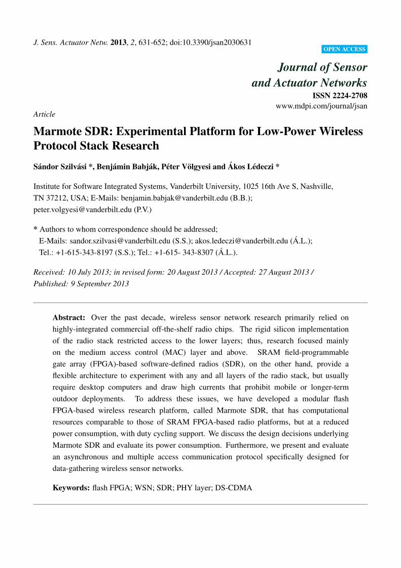
In order to evaluate the resource usage of a simple radio transceiver application and the powerconsumption of the Marmote SDR platform in various power modes, we implemented a simple PHYlayer using the above described framework. We chose binary FSK modulation to compare with therepresentative CC1000 [4] commodity radio used by the MICA2 and TelosB WSN nodes. The FSKmodem-based PHY layer has been implemented in the flash FPGA fabric with software-driven controlfunctions running on the MSS. Thus, the analysis of such reference design gives valuable insight intohow the flash FPGA logic resources get utilized for PHY layers of similar complexity.
Table 1 summarizes the logic allocation for the FSK modem, along with the interface HDLcomponents. The entire prototype design utilizes 29.5% of the SmartFusion A2F500 logic resourceswith the APB and AFE interfaces, representing the infrastructure part of the FPGA design, using 12.7%and 0.5%, respectively. The resource requirement of the AFE interface is the same in every application,but that of the APB interface varies highly (4%–15%) based on the amount of registers defined onthe APB bus. Thus, in general, it leaves 85%–95% of the FPGA fabric for the user application. Ourprototype FSK baseband application takes 16.3% in total, indicating that the total amount of FPGAlogic resources allows for experimentation with modulation and demodulation techniques of significantlyhigher complexity.
Table 1. FPGA logic resource utilization.
Component Logic Utilization
APB interface 1,469 (12.7%)AFE interface 52 (0.5%)FSK application 1,882 (16.3%)Total 3,403 (29.5%)
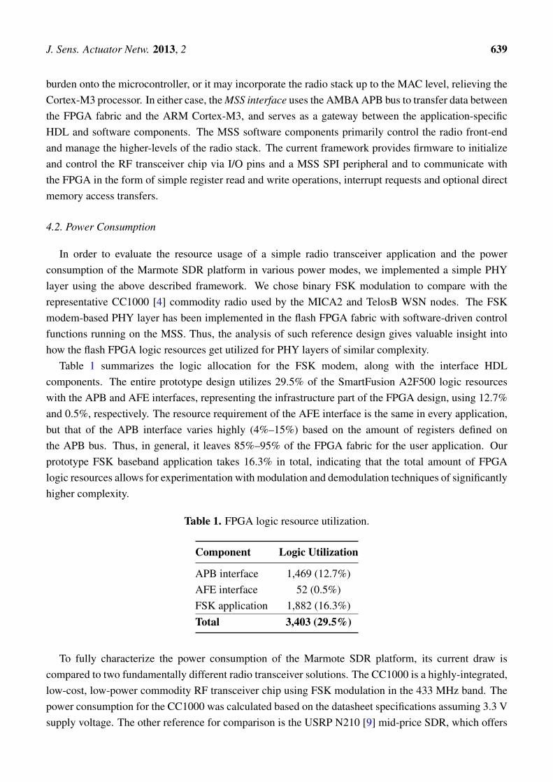
To fully characterize the power consumption of the Marmote SDR platform, its current draw iscompared to two fundamentally different radio transceiver solutions. The CC1000 is a highly-integrated,low-cost, low-power commodity RF transceiver chip using FSK modulation in the 433 MHz band. Thepower consumption for the CC1000 was calculated based on the datasheet specifications assuming 3.3 Vsupply voltage. The other reference for comparison is the USRP N210 [9] mid-price SDR, which offers
J. Sens. Actuator Netw. 2013, 2 640
full-stack design flexibility at a higher price and power consumption. (Note that the power consumptionof the embedded series USRP platform, the E100, is actually higher than that of the N210, accordingto their datasheet.) The latter was calculated based on the measured total current draw of the USRP at6 V with an SBX daughterboard attached to it. Thus, this value does not include the consumption of thedesktop computer that is additionally required for the operation. The Marmote SDR power consumptionwas measured by the Yellowstone power supply monitor and included the consumption of the Joshuaradio front-end and the Teton mixed-signal processing board, with the SmartFusion MSS, FPGA fabricand the AFE running at 10 MHz. (Note that unlike desktop SDR platforms, the Marmote SDR operationdoes not require a desktop computer.)
Figure 3. Power consumption comparison of the CC1000 commodity radio-frequency (RF)chip, the Marmote SDR platform and the USRP N210 in various power modes.
0 mW
5000 mW
10000 mW
15000 mW
Sleep Receive Transmit
CC1000
Marmote SDR
USRP N210
1 71
10560
24 287 852 34
14400 14700
The power consumption of the three approaches are compared in Figure 3 in three common scenariosin WSN duty cycle operation: sleep, transmit and receive mode. As WSN nodes usually spend mostof their time dormant; sleep mode is expected to reduce current draw to a fraction of that of activemodes. The CC1000 offers true sleep mode with power consumption less than 1 mW, the MarmoteSDR consumes 70.8 mW, while the USRP N210 does not provide similar low-power feature. In-depthanalysis of the Marmote SDR sleep mode showed that the Teton module is responsible for 72% of theMarmote SDR dissipated 70.8 mW, while the Joshua module for the remaining 28%. During sleep mode,all external peripherals were disabled, making the SmartFusion SoPC the main contributor to the 50 mWconsumed. Unfortunately, the current SmartFusion MSS lacks advanced low-power modes that achievesub-1 mW sleep power without turning the power rails off. Switching the power rails off has the adverseeffect of the eSRAM losing its content and, therefore, the application losing its state. As reinitializingthe application, saving and restoring its state variables results in significant wake up time penalties, wedefined the SmartFusion sleep mode with the integrated AFE and ACE powered off, the FPGA put inreset mode, the required MSS peripherals running on 32 kHz and the Cortex-M3 halted, waiting forinterrupt. We found the latter SmartFusion configuration to yield the lowest-power mode from whichthe system can wake up in only a few clock cycles. While the 50 mW power draw is significantlyhigher than that of our previous microcontroller plus IGLOO flash FPGA approach [17], we considerit a trade-off for the high-bandwidth, on-chip AMBA APB interface between the MSS and the FPGAfabric. As microcontrollers with ultra-low-power sleep mode already exist and the IGLOO flash FPGAsconsume less than 60 µW in Flash*Freeze mode [23], we expect manufacturing technology to lower the
J. Sens. Actuator Netw. 2013, 2 641
static power consumption for next generation flash FPGA-based SoPCs significantly. The Joshua radiofront-end had two main components, the MAX2830 transceiver chip and the TCXO during sleep modemeasurements. As the RF transceiver chip consumes <1 mA in shutdown mode, the main contributorto the 20 mW power is the TCXO. Even though the current Joshua module always keeps the TCXO on,this was a design decision, and it could be turned off in future versions.
In receive mode, Marmote SDR consumes 287.4 mW, approximately 12-times more power than theCC1000 (24.4 mW) and 50-times less than the USRP N210 (14,400 mW). Out of the 287.4 mW, theTeton board SmartFusion and AFE dissipate approximately 80 mW and 15 mW, while the MAX2830and the TCXO on the Joshua board, around 172 mW and 20 mW, respectively. Comparing the transmitmode power consumption at 0 dBm nominal transmit power, the Marmote SDR dissipates 851.7 mW,the CC1000, 24-times less (34.3 mW), while the USRP N210, 51-times more (14700 mW). TheSmartFusion, AFE and TCXO consume the same as in receive mode, while the MAX2830 transmitsection and the integrated power amplifier draw roughly 280 mW and 450 mW, respectively.
Thus, considering a 6,000 mAh 3.7 V Li-Ion battery, the Marmote SDR is able to continuously operatefor over 24 h in transmit mode (0 dBm) and to run for over 10 days in sleep mode.
5. Communication Protocol Design
Having discussed the design of the Marmote SDR platform debuting a simple FSK-based PHY layerdesign in Sections 3 and 4, this section focuses on the development and evaluation of a more advancedcommunication protocol PHY layer for WSNs. A fundamental task of the wireless communication in aWSN is to transfer the sensory data from the low-complexity and power-constrained sensor nodes to aresourceful base station. This task has generally been achieved using sensor nodes equipped with highlyintegrated RF chips and base station nodes of essentially the same architecture, but attached to a laptop ordesktop computer. The disadvantage of this approach is that it prescribes the use of a CSMA or TDMAaccess scheme throughout the network, including the base station vicinity, thus, it fails to take advantageof the increased resources usually available at the base station. However, if the PHY layer between aresourceful base station and the directly connected sensor nodes could be redefined, it would allow forexperimentation with other multiple access schemes. One potentially beneficial candidate for WSNs isasynchronous DS-CDMA, which holds the following promises:
• Collision-free multiple-access scheme that allows for simultaneous packet transmissions andreduced packet losses, due to multiple access interference• Asynchronous, contention-free medium access that requires no synchronization (scheduling)
between sensor nodes• Asymmetric communication link shifts the processing burden from sensor nodes to the base station
(simple transmitter and complex receiver architecture)• Rejection of narrowband interference and jamming
The Marmote SDR platform provides a means to experiment with novel, full-custom physical layerdesigns by exploiting the direct access to the baseband signals at the sensor nodes. Therefore, wedeveloped a DS-CDMA-based protocol and evaluated its performance using a measurement setup withmultiple wireless sensor nodes and a base station, as depicted in Figure 4. In this setup, the sensor nodes
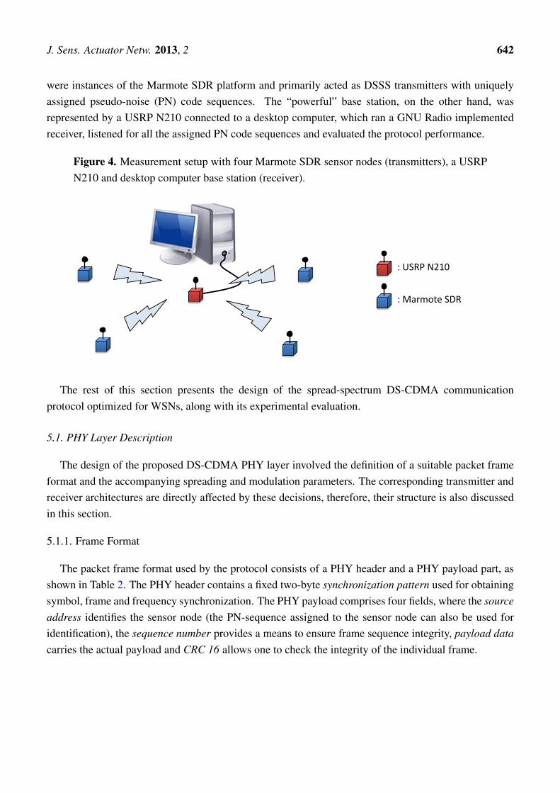
J. Sens. Actuator Netw. 2013, 2 642
were instances of the Marmote SDR platform and primarily acted as DSSS transmitters with uniquelyassigned pseudo-noise (PN) code sequences. The “powerful” base station, on the other hand, wasrepresented by a USRP N210 connected to a desktop computer, which ran a GNU Radio implementedreceiver, listened for all the assigned PN code sequences and evaluated the protocol performance.
Figure 4. Measurement setup with four Marmote SDR sensor nodes (transmitters), a USRPN210 and desktop computer base station (receiver).
: USRP N210
: Marmote SDR
The rest of this section presents the design of the spread-spectrum DS-CDMA communicationprotocol optimized for WSNs, along with its experimental evaluation.
5.1. PHY Layer Description
The design of the proposed DS-CDMA PHY layer involved the definition of a suitable packet frameformat and the accompanying spreading and modulation parameters. The corresponding transmitter andreceiver architectures are directly affected by these decisions, therefore, their structure is also discussedin this section.
5.1.1. Frame Format
The packet frame format used by the protocol consists of a PHY header and a PHY payload part, asshown in Table 2. The PHY header contains a fixed two-byte synchronization pattern used for obtainingsymbol, frame and frequency synchronization. The PHY payload comprises four fields, where the sourceaddress identifies the sensor node (the PN-sequence assigned to the sensor node can also be used foridentification), the sequence number provides a means to ensure frame sequence integrity, payload datacarries the actual payload and CRC 16 allows one to check the integrity of the individual frame.

J. Sens. Actuator Netw. 2013, 2 643
Table 2. Frame format and field lengths (bytes) used in the experimental protocol.
PHY Header PHY Payload
Sync pattern Source address Sequence number Payload data CRC 162 1 2 15 2
5.1.2. Spreading and Modulation
The proposed communication protocol employs direct-sequence spread spectrum (DSSS) modulationtechnique, where the transmitted data symbols are multiplied by an independent pseudo-noise (PN)sequence of “chips”, as shown in Figure 5. The spreading PN sequence has a significantly higher chiprate than the original data symbols; therefore, it expands the bandwidth of the original signal accordingly.When the same PN sequence is precisely known and timed at the receiver, its correlation with thereceived noise-like signal allows for the reconstruction of the original data symbols; see Figure 5. Whenproperly constructed PN-codes are assigned to the sensor nodes, the communication links in the basestation vicinity effectively allow for an asynchronous DS-CDMA scheme.
Figure 5. Simplified block diagram of a direct-sequence spread spectrum(DSSS) transceiver.
Despreading Spreading
PN generator
PN generator
LO LO
Rx symbols Tx symbols
In the proposed DS-CDMA protocol, each sensor node is allocated a unique PN spreading sequence,and the same sequences are known a priori at the base station. Two fundamental performance measuresof the PN sequences are their auto-correlation and cross-correlation functions. The auto-correlationfunction is defined as:
Ri(τ) =
NcTc∫−NcTc
PNi(t) · PNi(t− τ)dt (1)
where Nc is the length of the PN sequence and Tc is the chip period. The auto-correlation function isexpected to have a high correlation peak at τ = 0 and close to zero value at τ 6= 0, to enable accuratedetection of the spread signals. Meanwhile, the cross-correlation function is defined as:
Ri,j(τ) =
NcTc∫−NcTc
PNi(t) · PNj(t− τ)dt (2)
where Nc is the length of the PN sequence and Tc is the chip period. Ri,j(τ) should have close to zerovalue for any τ , as it measures the agreement between sequences, PNi and PNj , and, consequently,characterizes the possible interference between the two transmitters using these spreading sequences.
J. Sens. Actuator Netw. 2013, 2 644
PN sequences with outstanding auto-correlation and good cross-correlation properties can begenerated using simple linear-feedback shift registers. The class of exactly 2L − 1 long sequences,which can be produced by L-stage shift registers, are called maximal-length sequences or, simply,m-sequences [24]. The proposed DS-CDMA protocol relies on m-sequences that have a correspondingperiod of 211 − 1. The nodes are assigned one of the 176 distinct m-sequences to spread thesynchronization and data symbols. The PN-generator is reset only at the start of the transmission, asopposed to after each data symbol. Therefore, the transmitter associates a different chip pattern witheach symbol, and the receiver follows this same “long-code” approach for PN sequence generation inorder to detect and despread the received signal. The binary data symbols are differentially encodedbefore spreading, and the spread chips are modulated onto the carrier using differential binary phase-shiftkeying (DBPSK modulation).
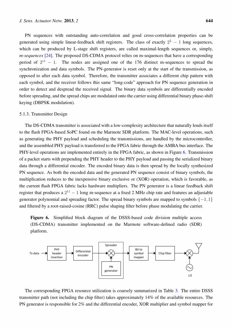
5.1.3. Transmitter Design
The DS-CDMA transmitter is associated with a low-complexity architecture that naturally lends itselfto the flash FPGA-based SoPC found on the Marmote SDR platform. The MAC-level operations, suchas generating the PHY payload and scheduling the transmissions, are handled by the microcontroller,and the assembled PHY payload is transferred to the FPGA fabric through the AMBA bus interface. ThePHY-level operations are implemented entirely in the FPGA fabric, as shown in Figure 6. Transmissionof a packet starts with prepending the PHY header to the PHY payload and passing the serialized binarydata through a differential encoder. The encoded binary data is then spread by the locally synthesizedPN sequence. As both the encoded data and the generated PN sequence consist of binary symbols, themultiplication reduces to the inexpensive binary exclusive or (XOR) operation, which is favorable, asthe current flash FPGA fabric lacks hardware multipliers. The PN generator is a linear feedback shiftregister that produces a 211 − 1 long m-sequence at a fixed 2 MHz chip rate and features an adjustablegenerator polynomial and spreading factor. The spread binary symbols are mapped to symbols {−1, 1}and filtered by a root-raised-cosine (RRC) pulse shaping filter before phase modulating the carrier.
Figure 6. Simplified block diagram of the DSSS-based code division multiple access(DS-CDMA) transmitter implemented on the Marmote software-defined radio (SDR)platform.
Spreader
PHY header
insertion
Differential encoder
Bit to symbol mapper
Chip filter
PN generator
LO
Tx data
The corresponding FPGA resource utilization is coarsely summarized in Table 3. The entire DSSStransmitter path (not including the chip filter) takes approximately 14% of the available resources. ThePN generator is responsible for 2% and the differential encoder, XOR multiplier and symbol mapper for
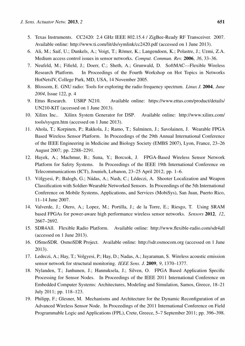
J. Sens. Actuator Netw. 2013, 2 645
less than 2% in total. Thus, similarly as in Section 4.2, the APB bus interface and configuration registerscontribute most to the 14.1%. The chip filter, on the other hand, is a 31-tap (finite impulse response) FIRfilter synthesized from a high-level design description with 16-bit coefficients. While it consumes 28.4%of the available total FPGA logic resources, the filter is a non-critical element, and its complexity couldbe greatly reduced without significant performance degradation.
Table 3. FPGA logic resource utilization of the DSSS transmit path.
Component Logic Utilization
DSSS transmitter 1,624 (14.1%)Chip filter 3,272 (28.4%)Total 4,896 (42.5%)
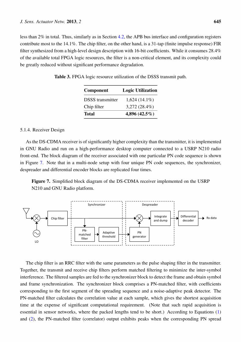
5.1.4. Receiver Design
As the DS-CDMA receiver is of significantly higher complexity than the transmitter, it is implementedin GNU Radio and run on a high-performance desktop computer connected to a USRP N210 radiofront-end. The block diagram of the receiver associated with one particular PN code sequence is shownin Figure 7. Note that in a multi-node setup with four unique PN code sequences, the synchronizer,despreader and differential encoder blocks are replicated four times.
Figure 7. Simplified block diagram of the DS-CDMA receiver implemented on the USRPN210 and GNU Radio platform.
Synchronizer Despreader
PN-matched
filter
Differential decoder
PN generator
Adaptive threshold
Integrate and dump
LO
Rx data Chip filter
The chip filter is an RRC filter with the same parameters as the pulse shaping filter in the transmitter.Together, the transmit and receive chip filters perform matched filtering to minimize the inter-symbolinterference. The filtered samples are fed to the synchronizer block to detect the frame and obtain symboland frame synchronization. The synchronizer block comprises a PN-matched filter, with coefficientscorresponding to the first segment of the spreading sequence and a noise-adaptive peak detector. ThePN-matched filter calculates the correlation value at each sample, which gives the shortest acquisitiontime at the expense of significant computational requirement. (Note that such rapid acquisition isessential in sensor networks, where the packed lengths tend to be short.) According to Equations (1)and (2), the PN-matched filter (correlator) output exhibits peaks when the corresponding PN spread

J. Sens. Actuator Netw. 2013, 2 646
synchronization pattern is found, but remains insensitive for patterns spread by other PN sequences,see Figure 8. The adaptive threshold logic determines the peak indexes and sets the time base for thedespreader block to reconstruct the PHY payload from the spread packet.
Figure 8. The output of the PN-matched filter in the synchronizer, showing distinctpulses at the start of five spread packet frames and insensitivity to noise and other ongoingnetwork traffic.
Figure 9. The amplitude (blue) and phase (red) of the integrate and dump block output foran inaccurately (left) and an accurately (right) synchronized packet.

J. Sens. Actuator Netw. 2013, 2 647
The despreader block is essentially a serial correlator, where the PN generator realizes a 211 − 1
long m-sequence through a linear-feedback shift register. The PN generator is reset and triggered by thesynchronizer block to properly time the onset of the integrate-and-dump block, performing:
Ik(τ) =
(k+1)NpTc∫kNpTc
r(t− τ) · PNi(t) dt 0 ≤ k < K (3)
where Ik(τ) is the integrator output for the kth payload symbol, Np is the spreading factor, Tc is the chipperiod, r(t) is the complex chip-filtered signal, PNi(t) is the despreading PN sequence of the ith receiver,τ is the assumed onset of the first payload symbol and K is the number of payload symbols. Figure 9shows that the phase of the integrator output is noise-like when inaccurately synchronized. However,in the case of accurate synchronization, its amplitude steadily builds up and its phase remains stable,allowing for proper non-coherent demodulation in the differential decoder.
5.2. Evaluation
The primary goal of the protocol evaluation was to characterize the PHY layer performance in areal-world scenario. For that, the PHY layer protocol was implemented using Marmote SDR nodes andan USRP N210/GNU Radio base station. The configured nodes were deployed in an office environment,and the packet reception ratio was registered under varying traffic load, using a different number of nodesand different spreading factors.
5.2.1. Experiment Setup
The three measurements scenarios involved 1, 2 or 4 Marmote SDR nodes and a USRP/GNU Radiobase station deployed in an office environment; the four-node setup is shown in Figure 4. The radios weretuned to 2.405 GHz, with the nodes continuously transmitting packets and the base station evaluating theaverage packet reception ratio based on 1,000 transmitted packets. The packets frames were constructedon the Marmote SDR nodes based on the format described in Section 5.1.1, each carrying a payload of20 bytes. To control the traffic load, the packet transmission was initiated periodically with a predefinedaverage τavg interval having 20% jitter. That is, the interval between two consecutive packet transmissionwas calculated according to:
∆τ = τavg(1 + 0.2 · U [-1, 1]) (4)
where U [·] denotes the uniform distribution. The chip rate was fixed at 2 MHz for all cases; therefore,the spreading factor values 8, 16 and 32 reduced the data rate to 250 kbps, 125 kbps and 62.5 kbps,respectively.
The GNU Radio-implemented receiver, run on an USRP N210 connected to a desktop computer,listened for all sensor nodes and kept track of the packet reception ratio (PRR) for each based on thereceived sequence number and CRC 16 fields. For each measurement, the receiver spreading factorwas set manually to match that of the transmitters, while the power control was adjusted based on theperceived PRR.

J. Sens. Actuator Netw. 2013, 2 648
5.2.2. Results
The single-node measurement was used to create a baseline with interference coming from theenvironment only. The results plotted in Figure 10 show that a reliable communication link wasestablished independently of the spreading factor used. The packet delivery ratio was 100%, regardlessof the traffic load, as one would expect for a contention-free and clear channel.
Figure 10. Packet reception ratio for the single-node setup under various traffic loads withspreading factors of 8, 16 and 32.
0%
10%
20%
30%
40%
50%
60%
70%
80%
90%
100%
1 2 3 4 5 6 7
Ave
rage
pac
ket
rece
pti
on
rat
io
Average transmission duty cycle
Single-node measurement
SF = 8
SF = 16
SF = 32
100% 50% 33% 25% 20% 17% 14%
The two-node measurement introduces multiple access interference (MAI) to the channel, as shownin Figure 11, which clearly impacts the packet delivery ratio for the low processing gain case. Underheavy traffic conditions, the average packet delivery ratio dropped to 71% for a spreading factor of 8 andto 99% for that of 16. Examination of the received data showed that packet losses were equally probabledue to missed detection of the synchronization header and to the corruption of the payload data.
Figure 11. Packet reception ratio for the two-node setup under various traffic loads withspreading factors of 8, 16 and 32.
0%
10%
20%
30%
40%
50%
60%
70%
80%
90%
100%
1 2 3 4 5 6 7
Ave
rage
pac
ket
rece
pti
on
rat
io
Average transmission duty cycle
Two-node measurement
SF = 8
SF = 16
SF = 32
100% 50% 33% 25% 20% 17% 14%

J. Sens. Actuator Netw. 2013, 2 649
The four-node setup further increased the MAI in the channel, creating a more realistic multi-nodescenario. The observed average packet delivery ratios depicted in Figure 12 show that with a spreadingfactor of 8, more than 16% of the packets were dropped in a low-traffic channel, approximately 50%were lost under moderate traffic and only 2% were delivered in high traffic. Increasing the processinggain to 16 improved the average packet reception ratio to over 90% in moderate network traffic, but itfalls down to 41% under heavy loads. Meanwhile, increasing the spreading factor to 32, the protocoldelivers over 96% of the packets on average, even in a highly loaded channel.
Figure 12. Packet reception ratio for the four-node setup under various traffic loads withspreading factors of 8, 16 and 32.
0%
10%
20%
30%
40%
50%
60%
70%
80%
90%
100%
1 2 3 4 5 6 7
Ave
rage
pac
ket
rece
pti
on
rat
io
Average transmission duty cycle
Four-node measurement
SF = 8
SF = 16
SF = 32
100% 50% 33% 25% 20% 17% 14%
In summary, our experiments showed that the designed DSSS communication protocol performsreliably when there is no contention in the channel. A processing gain of 8 already offered reasonableprotection against external interferences, such as the ongoing WLAN communication; however, as thenumber of nodes increased, such a low degree of spreading offered little protection against simultaneoustransmission, even under low traffic loads. Therefore, a truly collision-free DS-CDMA communicationcalls for reasonable spreading factors, which still remains a design parameter, primarily determined bythe size of the network and the expected network traffic. A detailed performance analysis with respectto these network parameters is given in [25]. In the presented experimental setup, the desired processinggain was attained by using a fixed chip rate and reducing the effective data rate. Alternatively, the datarate could be fixed, and the chip rate could be increased to achieve the same goal, without increasing thetransmitter complexity.
6. Conclusions
Long-term deployed WSN nodes face ultra-low-power requirements that have been combated onseveral fronts in the past decade. Power consumption of computational resources has been rapidlyreduced through advances in semiconductor process technology, but the same does not hold for theradio communication interface. Significant energy may be saved related to wireless communication inWSNs through the design of full-vertical communication protocol stacks tailored for the specific WSN

J. Sens. Actuator Netw. 2013, 2 650
application. Traditional WSN nodes utilize highly integrated off-the-shelf radio transceiver chips thatimplement the lower layers in ASIC and, therefore, reduce the design flexibility of those layers. SDRs,on the other hand, give full access to the entire stack and allow for rapid prototyping, but their powerconsumption is prohibitively large for practical battery-based operation.
In this paper, we presented the hardware design of the Marmote SDR platform, an experimentalresearch platform for WSN communication stacks. Through the flash FPGA-based SoPC architecture,the platform allows for rapid and flexible design of full network stacks from baseband processing in thePHY up to the application layer, which is not possible with integrated radio chips. The computationalresources offered by Marmote SDR are less than, but comparable to, that of desktop-connected SDRs.In return, the Marmote SDR consumes an order of magnitude less power than a desktop SDR, althoughstill significantly more than an integrated RF transceiver. The power consumption of Marmote SDR withthe Joshua 2.4 GHz radio front-end is approximately 0.25 W in receive and 0.8–1.5 W in transmit mode,depending on the transmit power. This allows for several hours-long battery based operation, which canbe further extended by duty cycling. Deployment of a Marmote SDR WSN with a prototype networkstack enables researchers to collect real world data on the communication protocol performance, ratherthan relying solely on simulation results—often prone to oversimplification. An experimentally-verifiedprotocol stack can then be implemented as a highly integrated transceiver, resulting in a much smallersize and a significantly smaller power budget. We believe that a platform like Marmote SDR can serveas a springboard for many novel low-power transceiver solutions in the future.
The hardware, HDL and software design files of the Marmote SDR platform are open-source andfreely available for download from [26].
Acknowledgments
This material is based upon work supported by the National Science Foundation under GrantsNo. 0964592 and No. 1035627.
Conflicts of Interest
The authors declare no conflict of interest.
References
1. Crossbow. Crossbow MICAz (MPR2400) Radio Module. Available online:http://www.xbow.com (accessed on 1 June 2013).
2. Polastre, J.; Szewczyk, R.; Culler, D. Telos: Enabling Ultra-Low Power Wireless Research.In Proceedings of the Fourth International Symposium on Information Processing in SensorNetworks (IPSN 2005), Los Angeles, CA, USA, 15 April 2005.
3. Bachir, A.; Dohler, M.; Watteyne, T.; Leung, K.K. MAC essentials for wireless sensor networks.IEEE Commun. Surv. Tutor. 2010, 12, 222–248.
4. Texas Instruments. Chipcon AS, CC1000: Single Chip very Low Power RF transceiver. 2004.Available online: www.ti.com/lit/ds/symlink/cc1000.pdf (accessed on 1 June 2013).
J. Sens. Actuator Netw. 2013, 2 651
5. Texas Instruments. CC2420: 2.4 GHz IEEE 802.15.4 / ZigBee-Ready RF Transceiver. 2007.Available online: http://www.ti.com/lit/ds/symlink/cc2420.pdf (accessed on 1 June 2013).
6. Ali, M.; Saif, U.; Dunkels, A.; Voigt, T.; Romer, K.; Langendoen, K.; Polastre, J.; Uzmi, Z.A.Medium access control issues in sensor networks. Comput. Commun. Rev. 2006, 36, 33–36.
7. Neufeld, M.; Fifield, J.; Doerr, C.; Sheth, A.; Grunwald, D. SoftMAC—Flexible WirelessResearch Platform. In Proceedings of the Fourth Workshop on Hot Topics in NetworksHotNetsIV, College Park, MD, USA, 14 November 2005.
8. Blossom, E. GNU radio: Tools for exploring the radio frequency spectrum. Linux J. 2004, June2004, Issue 122, p. 4
9. Ettus Research. USRP N210. Available online: https://www.ettus.com/product/details/UN210-KIT (accessed on 1 June 2013).
10. Xilinx Inc.. Xilinx System Generator for DSP. Available online: http://www.xilinx.com/tools/sysgen.htm (accessed on 1 June 2013).
11. Ahola, T.; Korpinen, P.; Rakkola, J.; Ramo, T.; Salminen, J.; Savolainen, J. Wearable FPGABased Wireless Sensor Platform. In Proceedings of the 29th Annual International Conferenceof the IEEE Engineering in Medicine and Biology Society (EMBS 2007), Lyon, France, 23–26August 2007; pp. 2288–2291.
12. Hayek, A.; Machmur, B.; Suna, Y.; Borcsok, J. FPGA-Based Wireless Sensor NetworkPlatform for Safety Systems. In Proceedings of the IEEE 19th International Conference onTelecommunications (ICT), Jounieh, Lebanon, 23–25 April 2012; pp. 1–6.
13. Volgyesi, P.; Balogh, G.; Nadas, A.; Nash, C.; Ledeczi, A. Shooter Localization and WeaponClassification with Soldier-Wearable Networked Sensors. In Proceedings of the 5th InternationalConference on Mobile Systems, Applications, and Services (MobiSys), San Juan, Puerto Rico,11–14 June 2007.
14. Valverde, J.; Otero, A.; Lopez, M.; Portilla, J.; de la Torre, E.; Riesgo, T. Using SRAMbased FPGAs for power-aware high performance wireless sensor networks. Sensors 2012, 12,2667–2692.
15. SDR4All. Flexible Radio Platform. Available online: http://www.flexible-radio.com/sdr4all(accessed on 1 June 2013).
16. OSmoSDR. OsmoSDR Project. Available online: http://sdr.osmocom.org (accessed on 1 June2013).
17. Ledeczi, A.; Hay, T.; Volgyesi, P.; Hay, D.; Nadas, A.; Jayaraman, S. Wireless acoustic emissionsensor network for structural monitoring. IEEE Sens. J. 2009, 9, 1370–1377.
18. Nylanden, T.; Janhunen, J.; Hannuksela, J.; Silven, O. FPGA Based Application SpecificProcessing for Sensor Nodes. In Proceedings of the IEEE 2011 International Conference onEmbedded Computer Systems: Architectures, Modeling and Simulation, Samos, Greece, 18–21July 2011; pp. 118–123.
19. Philipp, F.; Glesner, M. Mechanisms and Architecture for the Dynamic Reconfiguration of anAdvanced Wireless Sensor Node. In Proceedings of the 2011 International Conference on FieldProgrammable Logic and Applications (FPL), Crete, Greece, 5–7 September 2011; pp. 396–398.

J. Sens. Actuator Netw. 2013, 2 652
20. Kuo, Y.S.; Pannuto, P.; Schmid, T.; Dutta, P. Reconfiguring the Software Radio to Improve Power,Price, and Portability. In Proceedings of the 10th ACM Conference on Embedded NetworkedSensor Systems (Sensys’12), Toronto, ON, Canada, 6–9 November 2012.
21. Szilvasi, S.; Sallai, J.; Amundson, I.; Volgyesi, P.; Ledeczi, A. Configurable Hardware-basedRadio Interferometric Node Localization. In Proceedings of the 2010 IEEE AerospaceConference, Big Sky, MT, USA, 6–13 March 2010.
22. Microsemi. Total System Power. Available online: http://www.actel.com/documents/Power PIB.pdf (accessed on 1 June 2013).
23. Microsemi. IGLOO Low Power Flash FPGAs with Flash*Freeze Technology. Available online:http://www.actel.com/documents/IGLOO DS.pdf (accessed on 1 June 2013).
24. Simon, M.K.; Omura, J.K.; Sholtz, R.A.; Levitt, B.K. Spread Spectrum CommunicationsHandbook; Electronic communications, McGraw-Hill Professional Publishing: New York, NY,USA, 1994; pp. 283–284.
25. Geraniotis, E. Performance of noncoherent direct-sequence spread-spectrum multiple-accesscommunications. IEEE J. Sel. Areas Commun. 1985, 3, 687–694.
26. Marmote SDR Platform. Marmote low-power FPGA-based platform. Available online:http://marmote.googlecode.com (accessed on 1 June 2013).
c© 2013 by the authors; licensee MDPI, Basel, Switzerland. This article is an open access articledistributed under the terms and conditions of the Creative Commons Attribution license(http://creativecommons.org/licenses/by/3.0/).