market drivers for embedded component packaging
TRANSCRIPT
NAMIUM6.13 © 2013 TechSearch International, Inc.
Market Drivers for Embedded Components Packaging
E. Jan Vardaman, Linda C. Matthew, Karen Carpenter
TechSearch International, Inc.
www.techsearchinc.com
NAMIUM6.13 © 2013 TechSearch International, Inc.
Passive
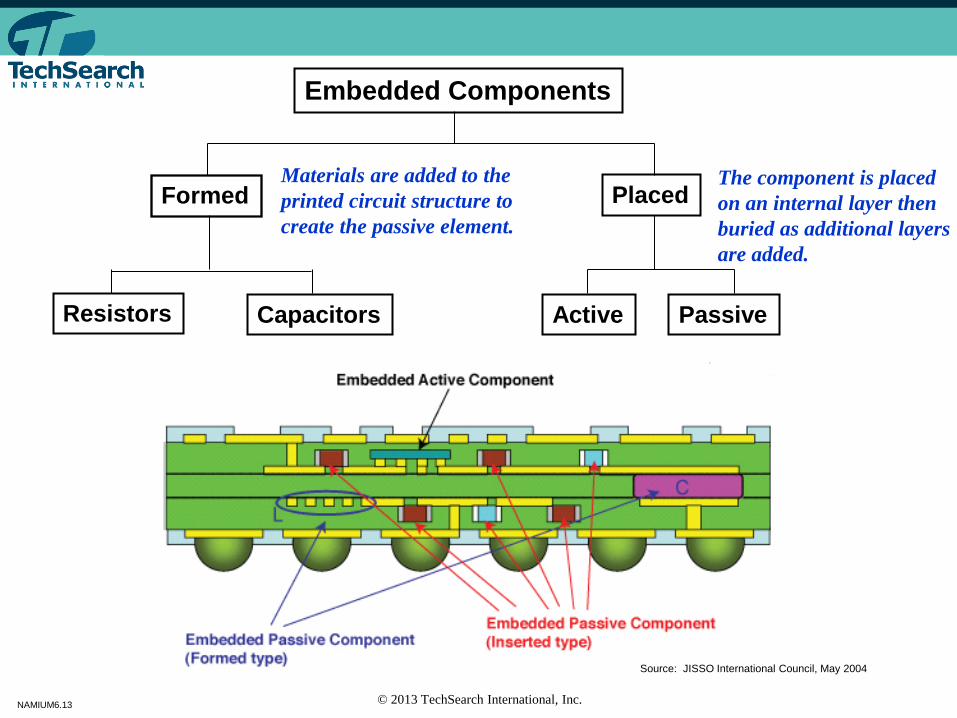
Embedded Components
Formed Placed
Active Capacitors Resistors
Materials are added to the
printed circuit structure to
create the passive element.
The component is placed
on an internal layer then
buried as additional layers
are added.
Source: JISSO International Council, May 2004
NAMIUM6.13 © 2013 TechSearch International, Inc.
Embedded in Substrates: A Look Back
• Companies embedding discrete passives into modules
– Module size reduction
– Improved performance
– Driven by trends in portable products
– Examples in production include products from Taiyo Yuden, DNP, etc.
– PCB with 250 components (0603s) embedded
• Many research projects and roadmaps
– European Hiding Dies project
– Fraunhofer “Chip in Polymer” process
– Casio and CMK EWLB consortium
– Motorola’s embedded passives demonstration vehicle
• Examples of embedded active components
– Casio watch modules (2006)
– Digital TV tuner modules (2006-2007)
– Ericsson mobile phone with RF device embedded in Clover’s PCB (200?)
– AT&S test vehicles (various)
– TI switching regulator (2010)
– Many demonstration vehicles
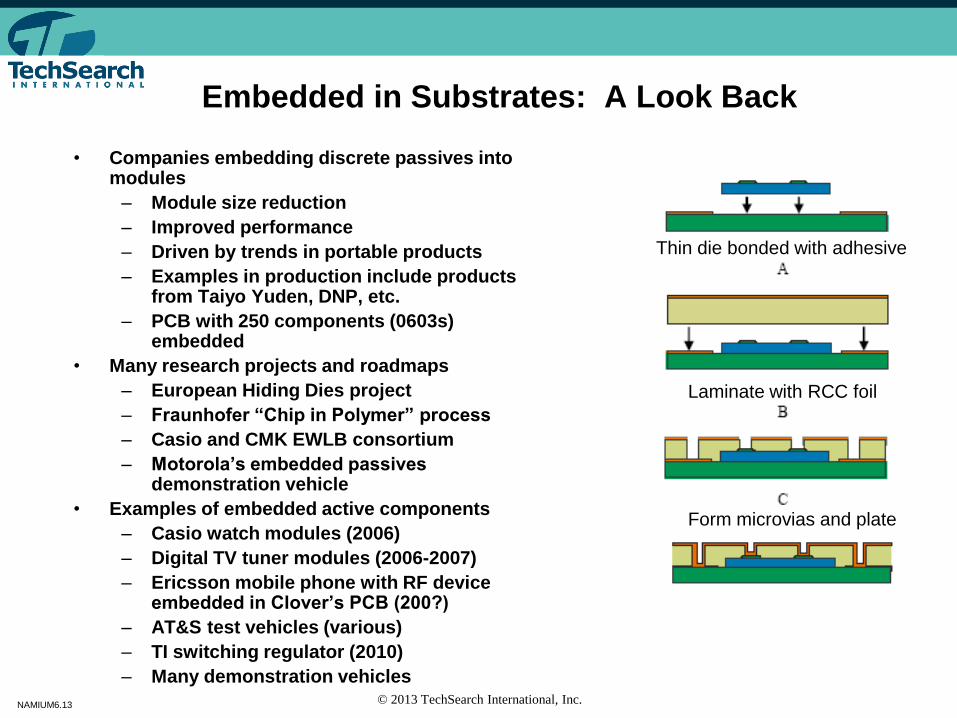
Thin die bonded with adhesive
Laminate with RCC foil
Form microvias and plate

NAMIUM6.13 © 2013 TechSearch International, Inc.
Casio, CMK, and Imbera Embedded Structures
• Casio embedded WLP in production in watch modules
• Casio, CMK, others in Japanese consortium—expect some
standards to emerge
• Imbera technology licensing agreements, but Imbera no longer
exists as a company developing technology
Source: Casio, CMK, and Imbera
NAMIUM6.13 © 2013 TechSearch International, Inc.
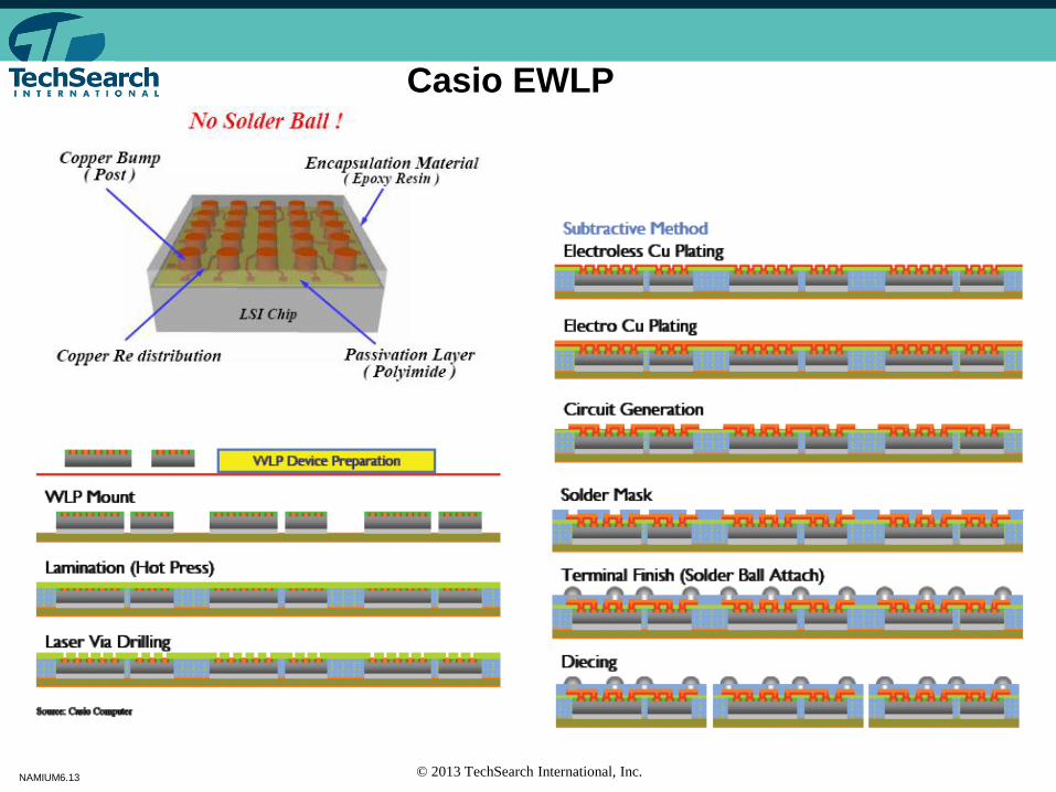
Casio EWLP
NAMIUM6.13 © 2013 TechSearch International, Inc.
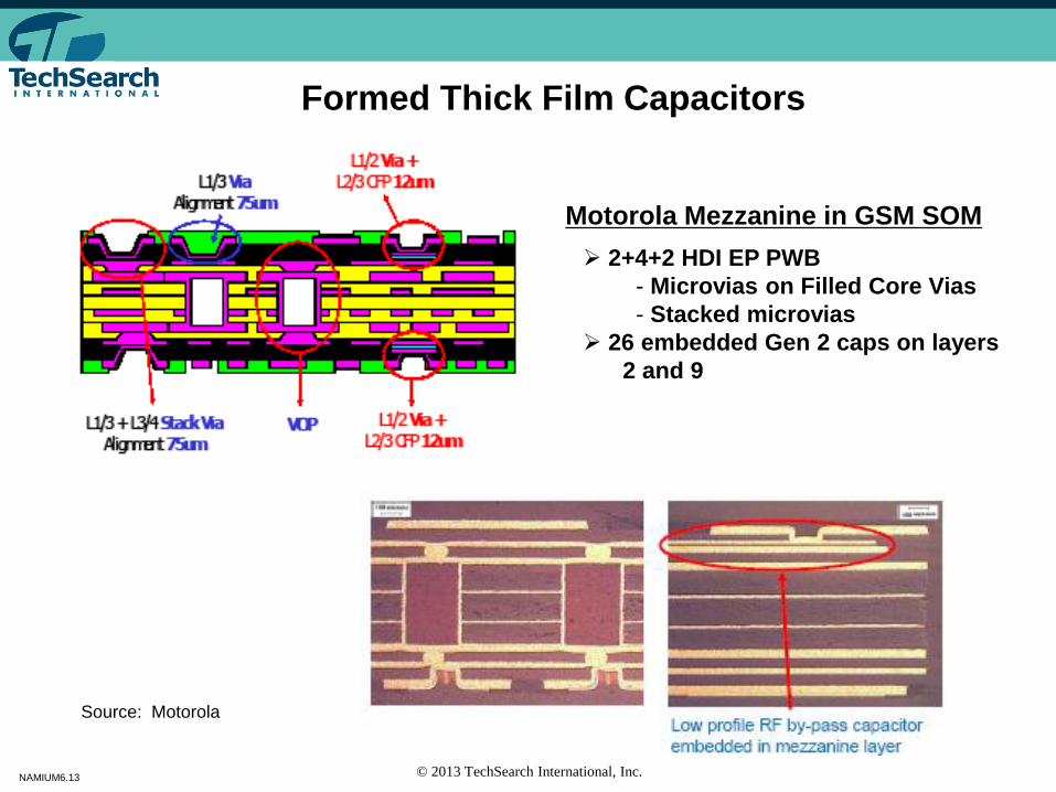
Motorola Mezzanine in GSM SOM
2+4+2 HDI EP PWB
- Microvias on Filled Core Vias
- Stacked microvias
26 embedded Gen 2 caps on layers
2 and 9
Formed Thick Film Capacitors
Source: Motorola
NAMIUM6.13 © 2013 TechSearch International, Inc.
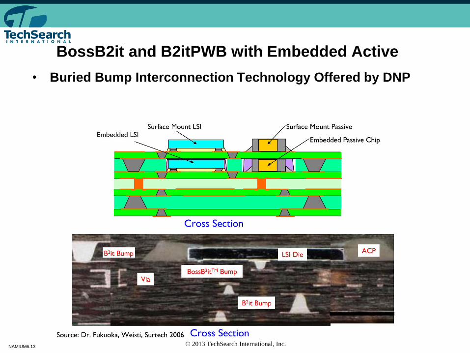
BossB2it and B2itPWB with Embedded Active
• Buried Bump Interconnection Technology Offered by DNP
NAMIUM6.13 © 2013 TechSearch International, Inc.
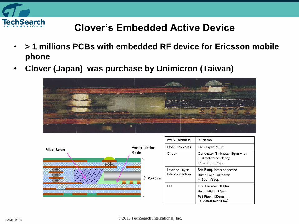
Clover’s Embedded Active Device
• > 1 millions PCBs with embedded RF device for Ericsson mobile
phone
• Clover (Japan) was purchase by Unimicron (Taiwan)
NAMIUM6.13 © 2013 TechSearch International, Inc.
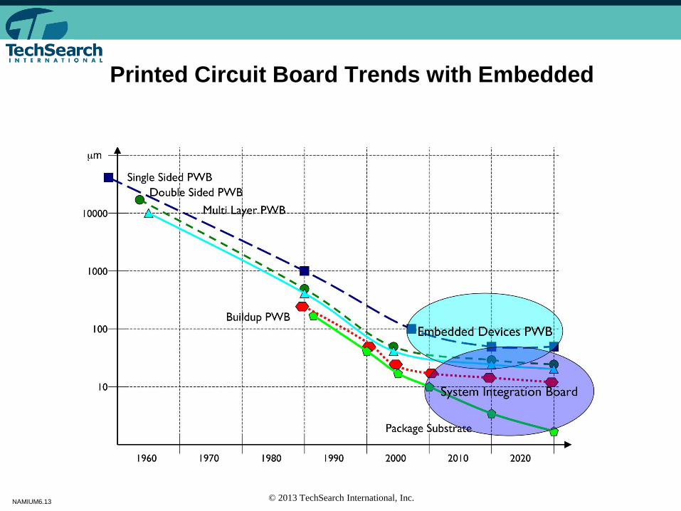
Printed Circuit Board Trends with Embedded
NAMIUM6.13 © 2013 TechSearch International, Inc.
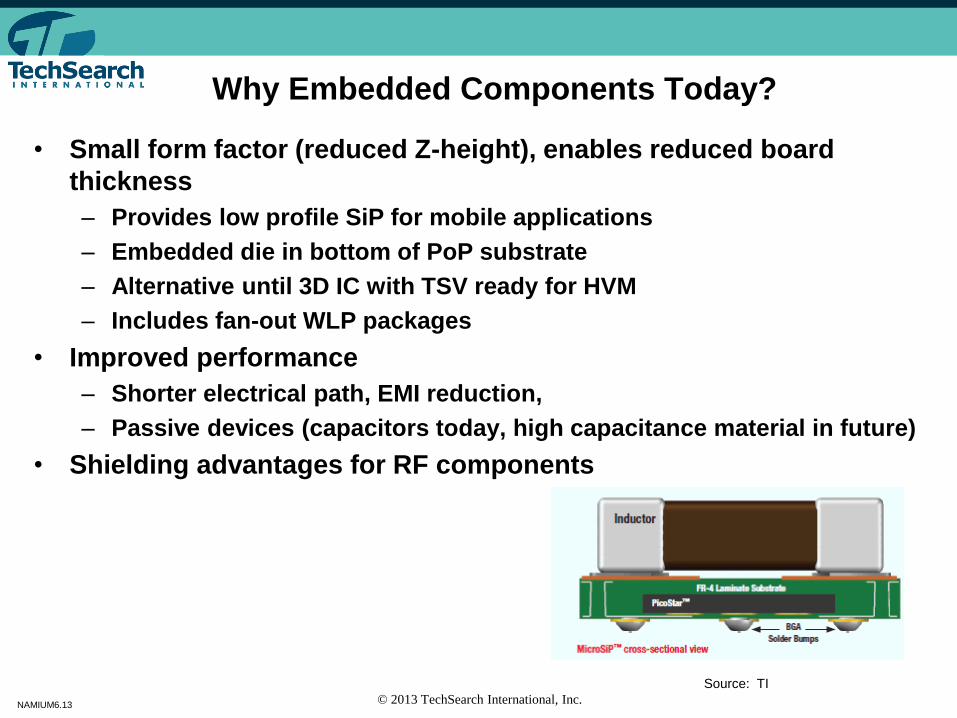
Why Embedded Components Today?
• Small form factor (reduced Z-height), enables reduced board
thickness
– Provides low profile SiP for mobile applications
– Embedded die in bottom of PoP substrate
– Alternative until 3D IC with TSV ready for HVM
– Includes fan-out WLP packages
• Improved performance
– Shorter electrical path, EMI reduction,
– Passive devices (capacitors today, high capacitance material in future)
• Shielding advantages for RF components
Source: TI
NAMIUM6.13 © 2013 TechSearch International, Inc.
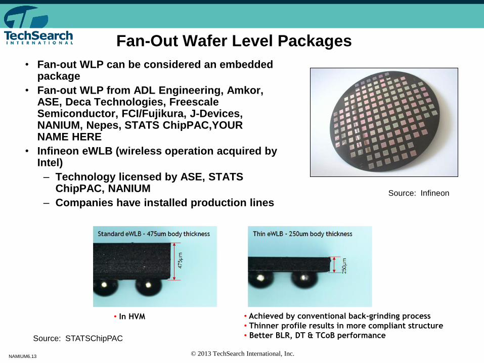
Fan-Out Wafer Level Packages
• Fan-out WLP can be considered an embedded package
• Fan-out WLP from ADL Engineering, Amkor, ASE, Deca Technologies, Freescale Semiconductor, FCI/Fujikura, J-Devices, NANIUM, Nepes, STATS ChipPAC,YOUR NAME HERE
• Infineon eWLB (wireless operation acquired by Intel)
– Technology licensed by ASE, STATS ChipPAC, NANIUM
– Companies have installed production lines
Source: Infineon
• Achieved by conventional back-grinding process
• Thinner profile results in more compliant structure
• Better BLR, DT & TCoB performance
• In HVM
Source: STATSChipPAC
NAMIUM6.13 © 2013 TechSearch International, Inc.
Projected Demand for Fan-Out WLPs in Units
• Unit shipments increased from 513 million units in 2011 to 616 million units in 2012
• Growth continues
• Multiple die can be packaged in fan-out, some panel configurations are used and can be
considered embedded die packages (EDPs)
• Demand for fan-out will increase if cost, reliability, and supply targets can be met
NAMIUM6.13 © 2013 TechSearch International, Inc.
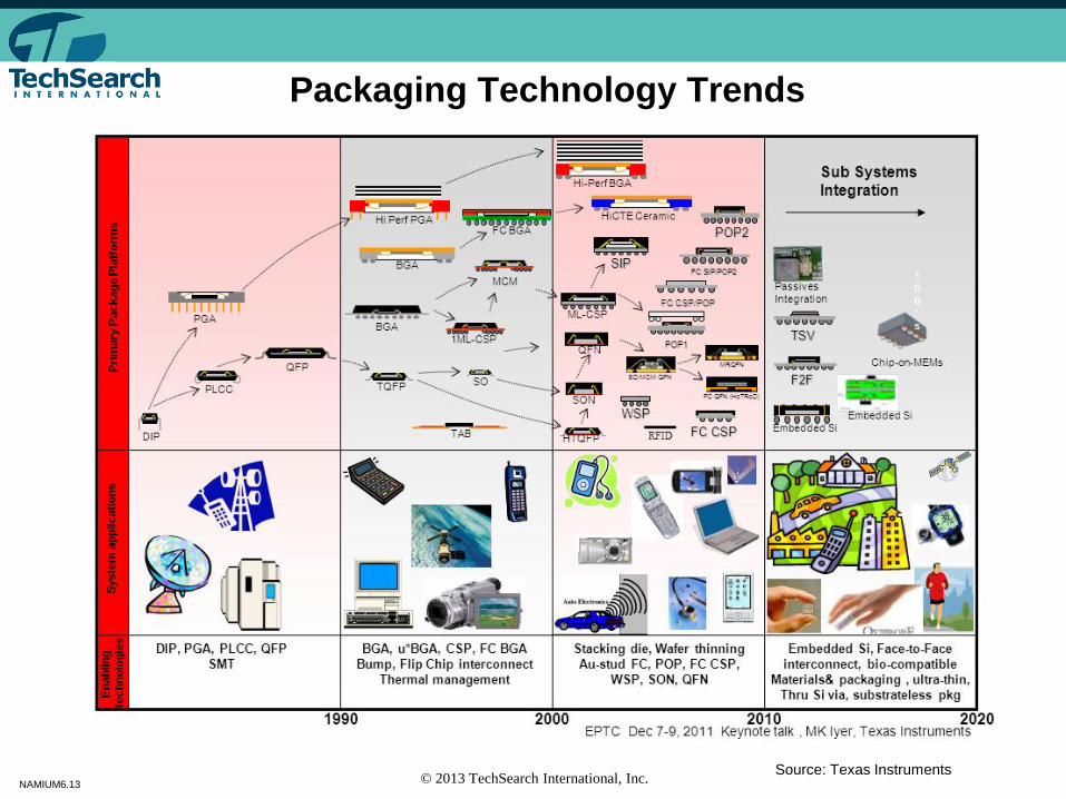
Packaging Technology Trends
Source: Texas Instruments
NAMIUM6.13 © 2013 TechSearch International, Inc.
Embedded Devices Today
• Embedded actives:
– Driver—package thinness
– Secondary advantages are improved robustness and security
– First applications—ultra-thin PoP for mobile products
– Technology—thin-film, laminated or build-up
– Companies with embedded die PoP activities ASE, AT&S, DNP, FlipChip International/Fujikura, J-Devices, NANIUM, Shinko Electric, STATS ChipPAC
• Embedded passives in IC packages and PCBs:
– Driver—decoupling capacitance close to the processor to enable higher operating frequencies
– First applications—application processors for mobile phones with embedded capacitors in production
– Mother board with MLCC/resistor
– Follow-on applications—high-end networking and communications
– Technology—primarily capacitors in build-up or laminated substrates
– Companies including Ibiden, DNP, Fujikura, Fuji Print, KOA, Meiko Electronics, Oki Print, Samsung Electro-Mechanics (SEMCO), Shinko Electric, Taiyo Yuden, TI, etc.
NAMIUM6.13 © 2013 TechSearch International, Inc.
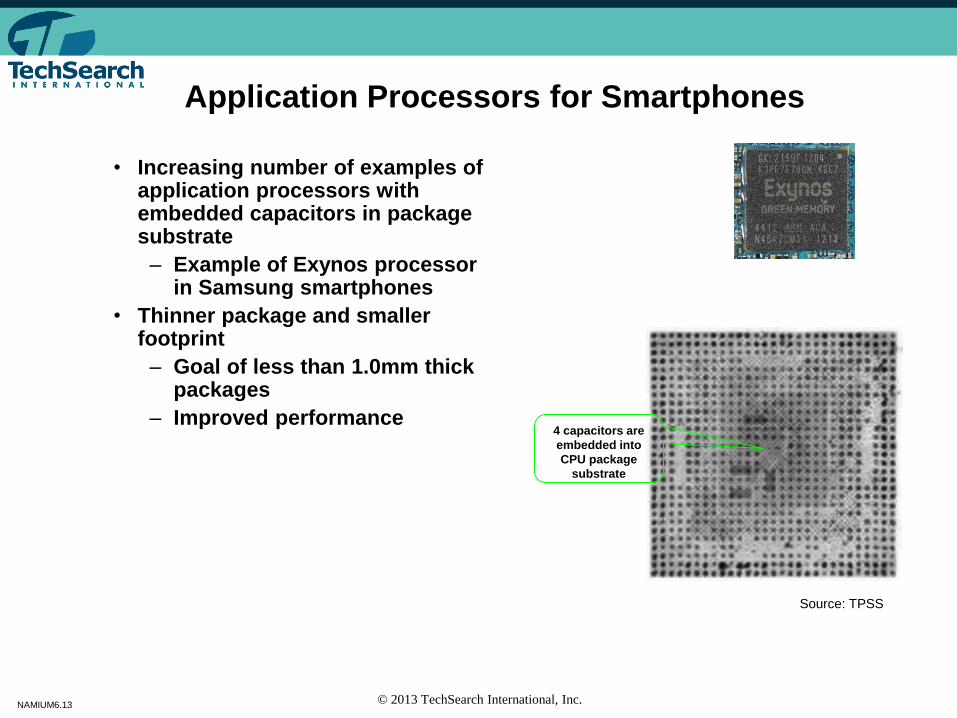
Application Processors for Smartphones
• Increasing number of examples of application processors with embedded capacitors in package substrate
– Example of Exynos processor in Samsung smartphones
• Thinner package and smaller footprint
– Goal of less than 1.0mm thick packages
– Improved performance
4 capacitors are
embedded into
CPU package
substrate
Source: TPSS

NAMIUM6.13 © 2013 TechSearch International, Inc.
DNP’s e-B2it™ Substrate with Embedded Active
• Coreless substrate with random or stacked vias
• WLP connected with solder attach or Au bump bare die
• Under evaluation for Near Field Communication/Radio Frequency (NCF/RF) modules, CMOS image sensors, and baseband processor modules
Source: Renesas
NAMIUM6.13 © 2013 TechSearch International, Inc.
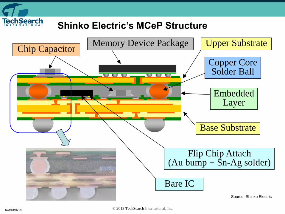
Base Substrate
Copper Core Solder Ball
Embedded Layer
Upper Substrate
Flip Chip Attach (Au bump + Sn-Ag solder)
Memory Device Package
Bare IC
Chip Capacitor
Shinko Electric’s MCeP Structure
Source: Shinko Electric
NAMIUM6.13 © 2013 TechSearch International, Inc.
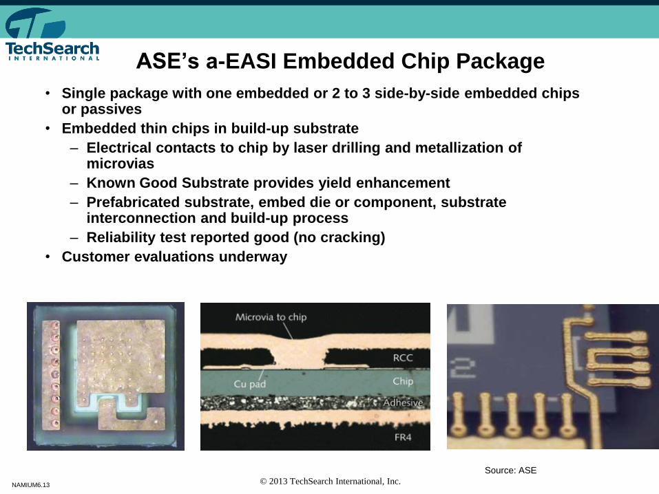
ASE’s a-EASI Embedded Chip Package
• Single package with one embedded or 2 to 3 side-by-side embedded chips or passives
• Embedded thin chips in build-up substrate
– Electrical contacts to chip by laser drilling and metallization of microvias
– Known Good Substrate provides yield enhancement
– Prefabricated substrate, embed die or component, substrate interconnection and build-up process
– Reliability test reported good (no cracking)
• Customer evaluations underway
Source: ASE
NAMIUM6.13 © 2013 TechSearch International, Inc.
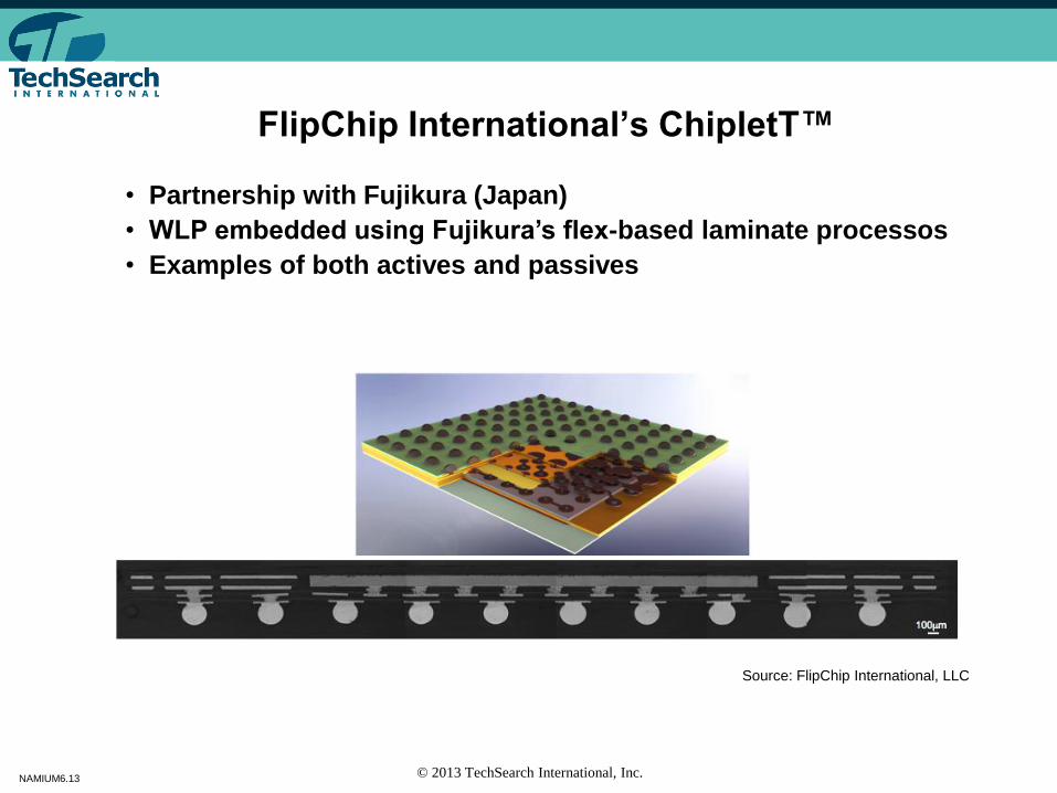
FlipChip International’s ChipletT™
Source: FlipChip International, LLC
• Partnership with Fujikura (Japan)
• WLP embedded using Fujikura’s flex-based laminate processos
• Examples of both actives and passives

NAMIUM6.13 © 2013 TechSearch International, Inc.
J-Devices WFOP™ Roadmap
• J-Devices (Japan) OSAT (Amkor/Toshiba ownership) developed embedded solution
• Die sits on metal plate (acts as heat spreader)
• RDL to fan-out die based on PCB technology
• Processed in panel
Source: J-Devices
NAMIUM6.13 © 2013 TechSearch International, Inc.
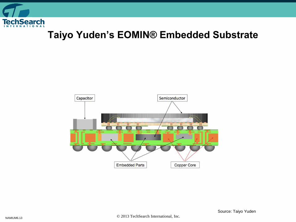
Taiyo Yuden’s EOMIN® Embedded Substrate
Source: Taiyo Yuden
NAMIUM6.13 © 2013 TechSearch International, Inc.
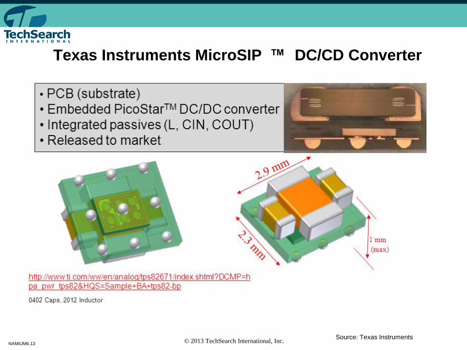
Texas Instruments MicroSIP�™ DC/CD Converter
Source: Texas Instruments

NAMIUM6.13 © 2013 TechSearch International, Inc.
Embedded Components Challenges
• Deviation from Traditional Assembly Model: OSAT needs substrate capability or close partner
• Assembly Yield
– Typical assembly process die are connect to known good substrates and assembly yield is typically greater than 99%
– Good die may be lost to substrate build-up process yield
– Companies working on strategies to minimize effect of substrate yield loss
• Cycle Time
– Substrate fabrication becomes a serial event in packaging flow so assembly cycle time similar to laminate substrate cycle time
– Laminate substrate cycle time is longer than traditional assembly cycle time
– Thin-film type process requires serial processing
• Functional testing of embedded die substrate in strip form
• Embedded die technologies appropriate for
– Embedding lower value, high yielding die where high interconnect density is required on both sides of the substrate
– RF modules where embedding tested die allows high density SMT on top
– Some analog parts
– Capacitors for improved performance
NAMIUM6.13 © 2013 TechSearch International, Inc.
Conclusions
• Embedded device market has arrived
– Driven by form factor and performance
• Solutions in the market today, more to arrive
– Embedded actives for PoP and other packages
– Embedded passives for application processor and other packages
– Embedded actives
• Issues with previous generation products being solved
– Thin die handling
– Use of high yielding die
– Assembly method improvements
– Cost reduction