maria maksimow transient current …lib.tkk.fi/dipl/2009/urn100049.pdftransient current technique...
TRANSCRIPT
helsinki university of technology
Faculty of Electronics, Communications and Automation
Maria Maksimow
TRANSIENT CURRENT TECHNIQUE (TCT) CHARACTERIZATIONOF SILICON PARTICLE DETECTORS
Thesis submitted for examination for the degree of Master of Science inTechnology
Espoo 26.3.2009
Thesis supervisor:
Prof. Harri Lipsanen
Thesis instructor:
D.Sc.(Tech.) Jaakko Harkonen

helsinki university of technology abstract of the
master’s thesis
Author: Maria Maksimow
Title: Transient Current Technique (TCT) Characterization of Silicon ParticleDetectors
Date: 26.3.2009 Language: English Number of pages: 8+53
Faculty: Faculty of Electronics, Communications and Automation
Professorship: Nanotechnology Code: S-104
Supervisor: Prof. Harri Lipsanen
Instructor: D.Sc.(Tech.) Jaakko Harkonen
In future high energy physics experiments, such as in the foreseen upgrade of the
particle accelerator LHC at CERN, particle detectors will be exposed to signifi-
cantly high particle radiation doses. Thus, extensive research is being conducted
on improving the radiation hardness of silicon particle detectors and various de-
fect and device engineering methods are examined. However, little data has been
gathered especially from p-type magnetic Czochralski silicon (MCZ-Si) devices.
This thesis presents the results of comparative transient current technique (TCT)
measurements of both n-type and p-type MCZ silicon detectors as well as n-type
Float Zone (FZ) silicon detectors. The results demonstrate that the MCZ silicon
devices have superior radiation hard properties in comparison with the FZ silicon
devices. Various examined parameters also suggest that p-type may be a more
radiation hard material solution for silicon detectors than n-type MCZ silicon.
Thus, replacing the currently installed FZ silicon detectors in LHC experiments
with either n-type or p-type MCZ-Si devices is a viable option.
Keywords: TCT, silicon, radiation hardness, MCZ-Si, particle detector

teknillinen korkeakoulu diplomityon
tiivistelma
Tekija: Maria Maksimow
Tyon nimi: Piihiukkasilmaisimien karakterisointi virtatransienttimenetelmalla
Paivamaara: 26.3.2009 Kieli: Englanti Sivumaara: 8+53
Tiedekunta: Elektroniikan, tietoliikenteen ja automaation tiedekunta
Professuuri: Nanotekniikka Koodi: S-104
Valvoja: Prof. Harri Lipsanen
Ohjaaja: TkT Jaakko Harkonen
Hiukkasilmaisimet altistuvat huomattavalle sateilylle tulevaisuudessa korkean
energian hiukkasfysiikkakokeissa, esimerkiksi kun CERN:n hiukkaskiihdytin
LHC ajanmukaistetaan. Nain ollen pii-ilmaisimien sateilynkestavyyden paran-
tamista eli erilaisten sateilyn aiheuttamien kidevirheiden seka ilmaisinsovellus-
ten muokkaamista tutkitaan laajasti. Magneettisella Czochralski-menetelmalla
(MCZ) valmistetuista kiekoista prosessoituja p-tyypin ilmaisimia on kuitenkin
tarkasteltu melko vahan. Tassa tyossa verrattiin seka n- etta p-tyypin MCZ-
pii-ilmaisimia seka float zone -menetelmalla (FZ) valmistetuista kiekoista proses-
soituja n-tyypin ilmaisimia suorittamalla virtatransienttimittauksia (TCT). Tu-
lokset osoittavat, etta MCZ-piin sahkoiset ominaisuudet ovat huomattavasti
sateilynkestavampia kuin FZ-piin. Tutkittujen parametrien perusteella voidaan
myos paatella, etta p-tyypin MCZ-pii saattaa olla sateilynkestavampi ilmaisinma-
teriaali kuin n-tyypin MCZ-pii. Taman tyon tulokset tukevat siis oletusta, etta
LHC-kokeiden nykyisten FZ-pii-ilmaisimien vaihtaminen n- tai p-tyypin MCZ-
ilmaisimiin olisi varteenotettava vaihtoehto.
Avainsanat: TCT, pii, sateilynkestavyys, MCZ-pii, hiukkasilmaisin

iv
Preface
The work for this thesis was carried out in the CMS Tracker Project of the Helsinki
Institute of Physics. The experimental research for the thesis was conducted at
CERN in Geneva during summer 2008, and the thesis was written in autumn 2008
in the TKK Micronova facilities of the Helsinki University of Technology. The
purpose of the work was to examine the radiation hardness properties of silicon
particle detectors by Transient Current Technique measurements.
I would like to thank my supervisor Professor Harri Lipsanen for offering the pos-
sibility to work on this interesting subject. I am most indebted to my instructor
Dr. Jaakko Harkonen for such focused guidance especially during the experimental
part of the project. I am grateful for his patience in answering the same questions
over and over again while, most importantly, showing a meaningful direction for the
research project. I also wish to thank all the colleagues in the CMS Tracker Project
both at CERN as well as in Otaniemi and Kumpula, who created a pleasant and
often fun atmosphere I enjoyed working in.
I want to express heartfelt gratitude to my parents, Ursula and Paul, and my sister
Christina, who have always supported me in all aspects of life. I would have never
achieved anything without their love and trust. Finally, thank you, Robert, for
lighting the Finnish winter darkness for me.
Otaniemi, 26.3.2009
Maria Maksimow

v
Contents
Abstract ii
Abstract (in Finnish) iii
Preface iv
Contents v
Symbols and Abbreviations vi
1 Introduction 1
2 Silicon Detectors 6
2.1 p-n Junction . . . . . . . . . . . . . . . . . . . . . . . . . . . . . . . . 6
2.2 Particle Detectors . . . . . . . . . . . . . . . . . . . . . . . . . . . . . 11
3 Radiation Hardness 14
3.1 Effects of Radiation Induced Damage . . . . . . . . . . . . . . . . . . 16
3.2 Methods for the Improvement of Radiation Hardness . . . . . . . . . 18
3.3 Annealing . . . . . . . . . . . . . . . . . . . . . . . . . . . . . . . . . 22
4 Transient Current Technique Measurements 25
4.1 Determination of the Electric Field Distribution,Full Depletion Voltage, and Effective Trapping Time . . . . . . . . . 26
4.2 Measurement setup . . . . . . . . . . . . . . . . . . . . . . . . . . . . 31
4.3 Samples and Measurements . . . . . . . . . . . . . . . . . . . . . . . 32
5 Results and Discussion 36
5.1 Voltages of Full Depletion and Leakage Currents . . . . . . . . . . . . 36
5.2 TCT Characterization . . . . . . . . . . . . . . . . . . . . . . . . . . 38
5.3 Annealing Experiment . . . . . . . . . . . . . . . . . . . . . . . . . . 44
6 Summary 49
References 51

vi
Symbols and Abbreviations
Symbols
A active area of detectorC capacitanceCCE charge collection efficiencyCCEg geometrical factor of CCECCEt trapping induced factor of CCED thickness of detectorDn diffusion constant of electronsDp diffusion constant of holesE(x) electric fieldEmax maximum electric fieldEC energy level of conduction bandEF Fermi energy levelEg band gap energyEt activation energyEV energy level of valence bandEv electric field caused by unit potentialI(t) detector currenti(t) transient currentIleak leakage currentJ current densityJgen generation currentJn electron current densityJp hole current densityJs saturation currentkB Bolzmann’s constantLn diffusion length of electronsLp diffusion length of holesn density of electronsNeff effective doping concentrationneq 1-MeV neutron equivalentnp0 density of electrons on the p-side in equilibriumn0 injected electron densityNA density of acceptor impurity atomsNC density of states in the conduction bandND density of donor impurity atomsni intrinsic carrier concentrationNt density of deep levelsNV density of states in the valence bandp density of holespn0 density of holes on the n-side in equilibriumq elementary chargeQ collected chargeQ0 total induced chargeQc charge per unit area

vii
T absolute temperaturet timetdr drifting timeV potentialVbi built in potentialvdr charge carrier velocityVfd voltage of full depletionvt thermal velocityV ol active volume of detectorW width of depletion regionxn limit of depletion region on n-side−xp limit of depletion region on p-sideα current related damage rateǫs permittivity of semiconductorµn mobility of electronsµp mobility of holesΦeq 1-MeV neutron equivalent irradiationρ electric charge densityσ conductivityσe,h trapping cross sectionτdetrap detrapping time constantτeff effective trapping time constantτgen generation lifetime

viii
Abbreviations
ALICE A Large Ion Collider ExperimentATLAS A Toroidal LHC ApparatusCCE charge collection efficiencyCERN European Organization for Nuclear ResearchCID current injected detectorCMS Compact Muon SolenoidCSIC Consejo Superior de Investigaciones CientıficasCZ CzochralskiCZ-Si Czochralski siliconC–V capacitance – voltageDOFZ diffusion oxygenated float zone silicone-h electron – holeFZ Float ZoneFZ-Si Float Zone SiliconHEP high energy physicsIMB-CNM Instituto de Microelectronica de Barcelona –
Centro Nacional de MicroelectronicaI–V current – voltageLHC Large Hadron ColliderLHCb Large Hadron Collider beautyMCZ magnetic CzochralskiMCZ-Si magnetic Czochralski siliconMIP minimum ionizing particleNIEL non-ionizing energy losspoly-Si polycrystalline siliconPS CERN Proton SynchrotronRD39 CERN Collaboration: Cryogenic Tracking DetectorsRD48 CERN Collaboration:
Research and development On Silicon for future Experiments (ROSE)RD50 CERN Collaboration:
Radiation hard semiconductor devices for very high luminosity collidersSCR space charge regionSCSI space charge sign inversionSi siliconSNR signal to noise ratioTCT Transient Current TechniqueTKK Helsinki University of Technology

1 Introduction
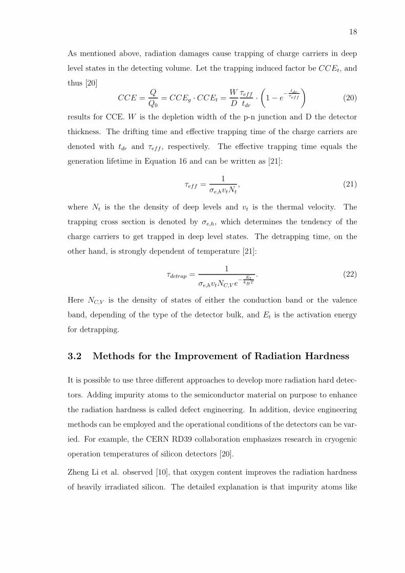
The year 2008 has witnessed a milestone in experimental high energy physics (HEP)
as the first beam circulated in the Large Hadron Collider (LHC) at the European
Organization for Nuclear Research CERN after more than twenty years of planning
and ten years of construction. The particle accelerator LHC, illustrated in Figure 1,
and its four main experiments are the largest physics experiment in the world. The
aim of the experiment is, among other things, to complete the Standard Model of
particle physics, namely by finding experimental proof of the existence of the Higgs
boson. [1]
Figure 1: The Large Hadron Collider LHC is located 100 m underground close toLake Geneva and the Jura mountains. [Image ©CERN]
The Higgs boson is believed to be a particle that transmits forces between matter
particles. It is predicted by the Standard Model, which is currently the underly-
ing theory of all particle physics. According to it, matter consists of two classes
of elementary particles: quarks and leptons. Fundamental interaction forces act
between these matter particles, the fermions, in form of energy exchange which is
performed by carrier particles, the bosons. E.g., the electromagnetic force is one of
these fundamental forces and the corresponding carrier particle is the photon.
The theory established by Peter Higgs and others suggests that both matter particles
and carrier particles interact with a special force field via the Higgs boson. The

2
interaction with this Higgs field provides particles with mass relative to the amount
of interaction. This would explain why some particles are heavier and others have
nearly no mass at all.
However, the Higgs boson has not been experimentally detected, yet. Although no
exact mass can be stated, it is predicted to be a rather heavy particle of more than
100 GeV/c2 but possibly even over 500 GeV/c2. Thus, the corresponding energy
range has to be scanned thoroughly as the energy of the single particle in turn
extends over a very small range. Moreover, a high repetition rate is needed, because
the Higgs boson is very rare and the background noise has to be averaged out, as
well. [2], [3]
Until now, experiments have not reached the required energies to observe the Higgs
particle. This is the reason for the massive size of the LHC and its experiments,
which also reach exquisite precision. The proton beams in the LHC consist of
bunches of protons that are injected into the ring with a frequency of 40 MHz. This
corresponds to collisions occuring within the detectors every 25 ns. The particle
flux reaches 107 1
sin the closest region to the interaction vertex [4]. But even with
this equipment, the production rate of the Higgs boson is expected to be rather
moderate. Calculations propose that it takes at least 2–3 years before any reliable
statistics have been collected from the data. [5]
The LHC itself is an accelerator ring built of 9300 magnets. It is located in a 27-
km-long tunnel 100 m underground close to Geneva and the French-Swiss border.
Protons or lead ions, which both belong to the group of hadrons, are accelerated
around the ring in both directions in separate beam pipes. The magnets bend and
focus the particle beam with such a high magnetic field that can only be achieved
if the magnets are superconducting. Hence, the operating temperature of the ac-
celerator magnets is only a few degrees from absolute zero. These procedures are
necessary to control the particle beams precisely as the particles reach speeds close
to light velocity and the energy of single protons rises up to 7 TeV. In fact, colliding
the beams requires the same precision as shooting two needles from 10 km apart to

3
hit each other in the middle [6].
Collisions of the particles occur at the four main experimental sites of the LHC:
ATLAS, CMS, ALICE, and LHCb. This work has been carried out in the framework
of the Compact Muon Solenoid (CMS) experiment. The CMS is a general-purpose
detector that is presented in Figure 2. While it is also designed for the search of
the Higgs boson, the CMS is a suitable particle detector for any appearing particles
with high energies reaching 2–3 TeV. Specific particles in this energy range and their
decays could lead to progress in verifying theories such as supersymmetry and string
theory. Research fields of dark matter, dark energy, and antimatter are desired to
profit from the experiment, as well. [7]
Figure 2: Schematic of the whole CMS Detector.[Image ©CERN]
A detector such as the CMS constitutes of a number of parts to identify different
particles reliably. The main parts of CMS are the tracker for spatial locating of
particle tracks, electromagnetic and hadronic calorimeters, and the muon system to
track muons which permeate through the other detector parts undetected. [8] The
all-silicon tracker system in CMS consists of different kinds of detectors [9]. Pixel
detectors are located closest to the interaction point because the requirements for
spatial resolution are the highest there. Behind the pixel detectors, silicon strip
detectors are installed. When the products of the particle collisions spread radially
from the collision point, obviously the silicon tracker is exposed to most extensive

4
particle radiation. The installation of the tracker system into the detector is shown
in Figure 3.
The ability of silicon to withstand the deterioration of performance caused by ra-
diation is called radiation hardness. However, the currently installed silicon pixel
detectors in CMS are predicted to reach the limits of their functionality approxi-
mately within the next five years, whereas the strip detectors are predicted to stay
functional for approximately ten years. This is the consequence of the excessive
radiation luminosities described earlier.
The detectors currently in CMS were processed from silicon fabricated by the Float
Zone (FZ) method. The purity of this type of silicon is considerably high and
FZ-Si has therefore been favored as detector material. In the beginning of the
1990’s the improving effect of oxygen on the radiation hardness of silicon was dis-
covered [10]. After excessive research in the field of oxygenated silicon and its
radiation hardness [11], the pixel detectors in CMS are indeed manufactured from
Diffusion Oxygenated Float Zone (DOFZ) silicon. However, the disadvantage of the
DOFZ method is the duration of the high temperature processing and therefore risk
of contamination and cost.
Figure 3: CMS Tracker installation.[Image ©CERN]
Approximately 10 years ago, development work in magnetic Czochralski (MCZ) crys-
tal growth of high-resistivity silicon began. Electronics and semiconductor industry

5
had also evolved a demand for high-resistivity silicon, and commercial availability of
high-resistivity MCZ-Si followed. Compared with FZ-Si, the oxygen concentration
in MCZ-Si is evidently higher to begin with. Additionally, as the most used silicon
type in industry, the growth of MCZ-Si is clearly less expensive than that of FZ-Si.
Thus, the work to develop radiation hard particle detectors for the LHC upgrade
from Czochralski silicon is of great interest.
A particularly well suited method for examining detectors is the Transient Current
Technique (TCT) that has been developed by researchers of the Ioffe Institute in St.
Petersburg, Russia and the Brookhaven National Laboratory in the USA [12]. It is
a nondestructive testing method that enables studies of highly irradiated detectors
more efficiently than, for example, traditional C–V measurements. TCT allows to
determine various parameters, such as the voltage of full depletion, to characterize
the detectors. Until now, little research has generally been conducted on p-type
MCZ-Si detectors. This thesis project focuses on comparative TCT measurements
of MCZ-Si detectors fabricated of both n- and p-type silicon bulk. Detectors of
FZ-Si are included in the studies as well for comparison.
This thesis presents in Chapters 2 and 3 the theoretical background for silicon par-
ticle detectors and their radiation hardness. Chapter 4 concentrates on the method
of TCT describing both the principle of the technique as well as the performed
practical measurements. The results are presented and discussed in Chapter 5, and
Chapter 6 summarizes the contents.

6
2 Silicon Detectors
Silicon particle detectors used in the LHC experiments are in principle reverse bi-
ased p-n diodes. The highly doped implantations are formed on both sides of the
silicon wafer to create volume devices. When the bias voltage is applied, the electric
field extends over the whole detector thickness. The energy of incoming particles
generates pairs of free charge carriers in the bulk that drift to opposite sides of the
detector and are collected there. Although Brattain and Bardeen developed the
point-contact transistor in the early 1950’s, it was W. Shockley who established the
theory of the p-n junction and suggested its practical use in electronic devices. The
theory presented in Section 2.1 is based on [13].
2.1 p-n Junction
In practice, a p-n junction is usually fabricated by diffusion or implantation of
acceptor- or donor-type impurity atoms into n- or p-type substrate silicon, respec-
tively. In theory, however, a p-n junction is usually described as an abrupt junction
combined of two originally independent parts; one part being p-type, the other
n-type. The term abrupt junction describes a state in which the impurity atom
concentration changes abruptly over the junction interface from acceptors to donor
atoms as depicted in Figures 4a) and 4b). Furthermore, a one-sided junction results
when the impurity density is significantly higher on one side of the junction than on
the other side.
When the p-type and n-type regions form a common interface, the free carriers of
both sides diffuse to the other side of the junction and recombine. Electrons move in
direction of the p-region and leave positive donor ions behind until xn. Negatively
charged acceptor ions occupy the p-type region until −xp as holes diffuse to the
n-side. The region containing the ionized impurity atoms is empty of free charge
carriers and is thus called the depletion region or space charge region (SCR). The
limits −xp and xn of the depletion region are shown in Figure 4. Thermal equilibrium
is reached when there is no net current flow.

7
Figure 4: Properties of an abrupt p-n junction: a) density of impurity atoms; b)space charge density; c) distribution of the electric field; and d) potential distributionover the junction.
The Fermi energy level EF in p-type semiconductors is close to the valence band
Ev and close to the conduction band Ec in n-type semiconductors. As a result, the
conduction and valence bands are bent in the junction region because the Fermi
level has to stay constant over the junction to satisfy the condition of zero current
flow. The bending of the energy bands leads to a built-in potential Vbi; i.e., qVbi
is the difference in energy between the original EF levels in the n- and p-regions.
For silicon p-n junctions, Vbi has a value of approximately 0.7 V. Vbi can as well be
understood as the corresponding potential to the electric field which is generated in
the depletion region between the space charges opposite in charge. The distribution
of potential over the junction is presented in Figure 4d).
The p-n junction can be described mathematically starting from Poisson’s equation
in one dimension:dE
dx=
ρ
ǫs
. (1)
E is the electric field across the junction and ǫs the permittivity of the semiconduc-
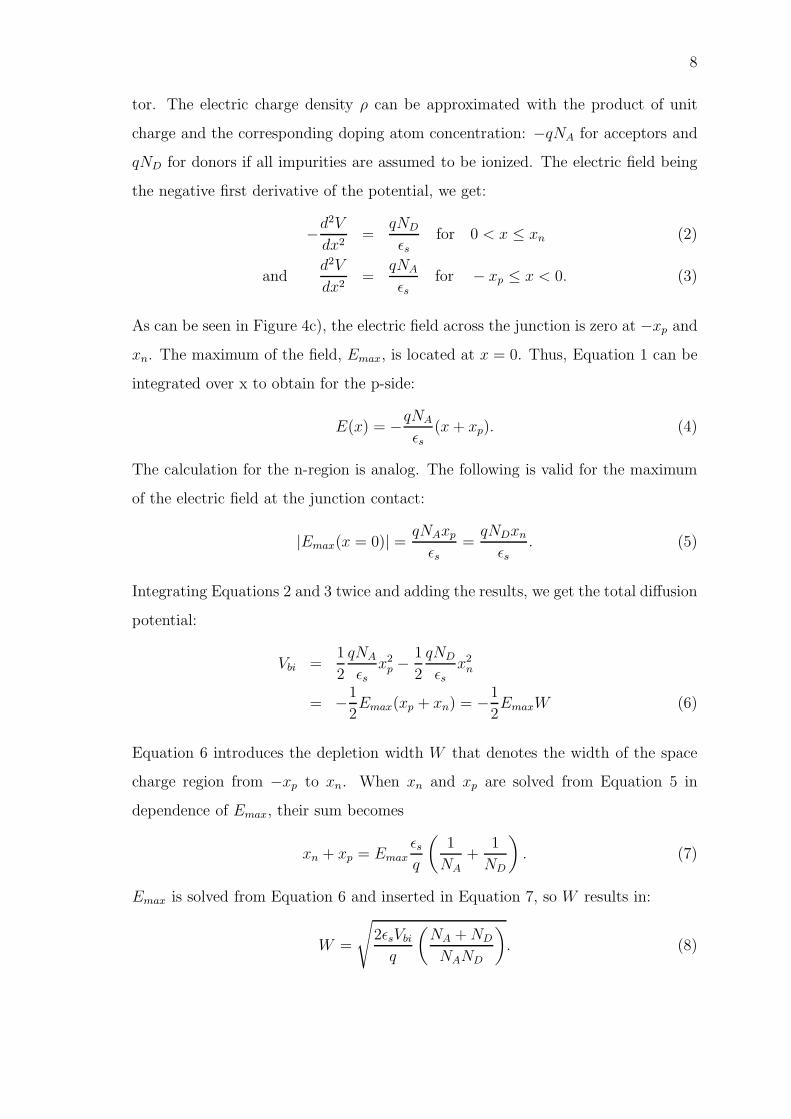
8
tor. The electric charge density ρ can be approximated with the product of unit
charge and the corresponding doping atom concentration: −qNA for acceptors and
qND for donors if all impurities are assumed to be ionized. The electric field being
the negative first derivative of the potential, we get:
−d2V
dx2=
qND
ǫs
for 0 < x ≤ xn (2)
andd2V
dx2=
qNA
ǫs
for − xp ≤ x < 0. (3)
As can be seen in Figure 4c), the electric field across the junction is zero at −xp and
xn. The maximum of the field, Emax, is located at x = 0. Thus, Equation 1 can be
integrated over x to obtain for the p-side:
E(x) = −qNA
ǫs
(x + xp). (4)
The calculation for the n-region is analog. The following is valid for the maximum
of the electric field at the junction contact:
|Emax(x = 0)| =qNAxp
ǫs
=qNDxn
ǫs
. (5)
Integrating Equations 2 and 3 twice and adding the results, we get the total diffusion
potential:
Vbi =1
2
qNA
ǫs
x2
p −1
2
qND
ǫs
x2
n
= −1
2Emax(xp + xn) = −
1
2EmaxW (6)
Equation 6 introduces the depletion width W that denotes the width of the space
charge region from −xp to xn. When xn and xp are solved from Equation 5 in
dependence of Emax, their sum becomes
xn + xp = Emax
ǫs
q
(
1
NA
+1
ND
)
. (7)
Emax is solved from Equation 6 and inserted in Equation 7, so W results in:
W =
√
2ǫsVbi
q
(
NA + ND
NAND
)
. (8)

9
If the junction is one-sided with ND >> NA, and it is assumed that neither the
depletion region extends over the limits of W nor are any charge carriers left in the
SCR, then Equations 5 and 6 yield:
W =
√
2ǫsVbi
qNA
. (9)
Again, the calculation is analog, if NA >> ND. The depletion width extends to the
side of the junction with lighter doping concentration, because the condition of total
charge neutrality has to be fulfilled. As a consequence, it is possible and desirable
to increase the depletion width through the whole detector thickness D by biasing
the detector with sufficient reverse voltage, namely the full depletion voltage Vfd.
Thus, when D = W , Equation 9 transforms to
Vbi − Vfd =qNAD2
2ǫs
(10)
for a one-sided p-type detector. According to Equation 10, the options to achieve a
depletion voltage as low as possible include reducing the doping concentration of the
bulk and using thin detectors. The effective doping concentration is often denoted
with Neff , when
Neff = ND − NA. (11)
Applied voltage V changes the charge per unit area, Qc, in the active detector
volume. This is the definition for the depletion-layer capacitance per unit area:
C ≡dQc
dV. (12)
Using Equation 9, C for a one-sided abrupt junction can be written as:
C =ǫs
W=
√
qǫsNA
2(Vbi − V ), W ≤ D, V ≤ Vfd (13)
When the external voltage reaches Vfd, the detector is fully depleted. As a result,
the overall capacitance saturates to a value solely dependent on geometrical factors:
C =ǫsA
D. (14)

10
A is the active area of the diode. Consequently, the voltage of full depletion can
be determined, e.g., by C-V measurements, from the saturation point of the capac-
itance.
The ideal diode law for current-voltage characteristics is the Shockley equation:
Js =qDppn0
Lp
+qDnnp0
Ln
, (15)
where Js is the saturated diffusion current when no electric field is present. Dp
(Dn) is the diffusion constant of holes (electrons), pn0 (np0) is the equilibrium hole
(electron) density on the n-side (p-side), and Lp (Ln) denotes the diffusion length
of holes (electrons).
In a reverse-biased detector, current is generated in the depleted layer, which is
exposed to an electric field. The generation current Jgen can be expressed as:
Jgen =qniW
τgen
, (16)
where τgen denotes the lifetime of generated charge carriers, and ni is the intrinsic
carrier concentration defined as:
n2
i = np = NCNV e−Eg
kBT . (17)
The effective densities of states are denoted with NC and NV for conduction band
and valence band, respectively. Eg is the band gap of the semiconductor, kB Bolz-
mann’s constant, and T the temperature.
Diodes are only partially depleted at low reverse bias voltage. In such circumstances,
the total reverse leakage current can be expressed as the sum of the diffusion current
Js from the non-depleted area and the generation current Jgen from the SCR. The
leakage current is also affected by other parasitic currents such as surface generation
current. This can however be neglected along with other unideal conditions such as
tunneling of charge carriers between energy states in the band gap and the series
resistance in the junction structure. In particle detectors, the minority charge carrier
concentration also remains significantly lower than the density of majority charge
carriers, thus excluding a high-injection case.

11
Consequently, Jgen becomes the dominant component of the leakage current when
diodes are fully depleted. Hence, the total leakage current of a fully depleted de-
tector can be approximated by Equation 16. Although τgen depends very weakly
on the temperature, the intrinsic carrier concentration ni is strongly temperature
dependent, as evident from Equation 17. Thus, the temperature dependence of the
generation current is highly significant.
2.2 Particle Detectors
A diode structure is operated under reverse bias in detecting mode, because detector
operation based on diffusion would not be fast enough to separate single signals from
each other. Collision events occur in the LHC in 25-ns intervals, and the signals
must be read out in each interval. This can only be achieved by reading out the
drift current caused by the electric field.
Practical implementations of detectors are usually based on lightly doped bulk ma-
terial with thin, high-resistivity, and highly doped implantations. This strongly
asymmetrical junction can be described with the theory of a one-sided abrupt junc-
tion as presented in the previous section. Traditional detectors have mostly been
fabricated from n-type bulk silicon. The front side is doped with acceptor-type im-
purities to create a p+-type implantation, and a n+-type implantation forms on the
back side as a result of donor doping. Thus, the p-n junction is formed close to the
front side of the detector.
During operation the detector is fully depleted by reverse bias. The carriers gen-
erated by the incident particles drift under the influence of the electric field to the
corresponding nodes of the bias voltage. This is illustrated in Figure 5, that indi-
cates, how the holes drift in the direction of the negative potential and the electrons
in that of the positive potential.
The band gap Eg of silicon is 1.17 eV, but additional energy is required to excite
electrons from the valence band to conduction band, thus creating electron-hole
(e-h) pairs. The band gap of silicon is indirect; therefore, there are changes in

12
+
-
p
n
n+
+
V-
+
particle track
+
+
+
+
+
-
-
-
-
-
Figure 5: Operational principle of a fully depleted silicon particle detector.
electron momenta when transitions of electrons occur in the band gap structure.
Consequently, excited phonons with a certain energy are needed to compensate the
momentum changes. Hence, the minimum energy for ionizing silicon diode structures
is 3.67 eV at room temperature. [14]
The minimum ionizing particles (MIP) create in a fully depleted 300-µm-thick silicon
detector about 22000 electrons, which corresponds to approximately 70 e-h pairs
per micron [14]. In order to achieve measurable signals from such level of carrier
concentration, the practical implementations of detectors are volume devices. This
enables collection of carriers from the entire detector bulk.
Single electrons drifting through a 300-µm-thick detector at an average electric field
of 104 V/cm are collected in approximately 10 ns, whereas the collection time for
holes is approximately 25 ns [14]. The collection times of the charge carriers depend
on their drift velocities, which, on the other hand, are determined by the mobilities
of electrons and holes, respectively. Thus, the time needed to collect the induced
charge carriers varies with temperature as the mobility of both electrons and holes
increases with decreasing temperature. Moreover, if the trapping probability of the
charge carriers is high, not all induced charge carriers can be collected, and the
total amount of the remaining free carriers can be read out in even shorter time
than stated above (see Section 3.1).

13
In HEP experiments two different detector principles are usually applied, pixel and
strip detectors. These terms refer to the segmentation of the implantations on the
detector surface. The aim of these segmentations is to enhance spatial resolution of
the detectors. For example, in CMS strip detectors, 4 x 128 or 6 x 128 detector-
long strips are implanted parallel on the substrate. Modern detectors often have
AC-coupled read-out electronics because this prevents additional coupling of the
leakage current.

14
3 Radiation Hardness
The tracking detectors in hadron colliders are exposed to significant radiation. To
make radiation fluences comparable regardless of the type and energy of the particle
beam, they are often expressed as equivalents to fluences of neutrons with the specific
energy of 1 MeV. This method is referred to as non-ionizing energy loss (NIEL)
scaling and is presented in detail in [15].
For example, in CMS [4], where at the hadron collision point several different elemen-
tary particles are created, the accumulated radiation during ten years of operation is
expressed as 1.6·1014 cm−2 1 MeV neutron equivalent (neq) fluence for the innermost
strip detectors in the middle of the tracking system. Moreover, the corresponding
value is 3.2 · 1015 neq/cm2 for the innermost pixel detectors at only 4-cm radius
from the center of the tracker barrel. Simultaneously, under such radiation, at least
the currently installed silicon pixel detectors will most probably deteriorate to an
intolerable level in performance [16].
High-intensity radiation damages the crystal structure of the silicon bulk. The
incoming energy can displace atoms in the silicon lattice, thus creating vacancies
and interstitials. If the incoming particles have sufficiently high energies, multiple
crystal defects are created that can cluster and cause larger damaged regions in
the bulk crystal as can be seen in Figure 6. It has been observed [17], that the
distribution of damage types depends on the type of the incoming particle.
Neutron irradiation results mainly in severe cluster defects, whereas light-energy
protons cause mostly individual displacements, i.e., point defects. On the other
hand, irradiation with high-energy protons, which fall under the category of fast
hadrons, causes both point defects as well as clusters. While the NIEL hypothe-
sis scales the equivalent energy losses well, it needs to be noted that the different
distribution of defect types for different types of radiation is not included in the
model.
Furthermore, the defects lead to three major effects. First of all, the current leakage

15
Cluster
Figure 6: Schematic illustration of damage induced by incoming radiation in adetector crystal.
increases because the crystal defects, that have energy states close to the middle of
the band gap, act as generation centers of charge carriers. Second of all, the effective
doping concentration Neff changes. The full depletion voltage Vfd is proportional
to Neff ; thus, increasing the absolute value of Neff results in the increase of Vfd.
Finally, the deep-level energy states of the defects trap free charge carriers. In this
case the charge collection efficiency (CCE) decreases, because the charge carriers
stay usually trapped for a longer period than the shaping time of the read-out
electronics.
Various methods have been investigated to improve the radiation hardness of sil-
icon devices and reduce the unwanted effects caused by the damages. Both the
macroscopic effects resulting from radiation induced defects and the most successful
approaches for enhancing radiation hardness are discussed in the following sections.
16
3.1 Effects of Radiation Induced Damage
As explained in Section 2.1, the main source of leakage current in silicon detectors
is the generation current in the depletion region. Irradiation defects increase the
number of generation centers in the detector bulk, and this leads to growing leakage
current. Although the defects are crystallographic, the crystallographic orientation
does not influence the increase of the leakage current after proton irradiation, as do
not the initial doping concentration or other characteristics of the detector material
either. The current growth ∆I is rather proportional to the irradiation fluence as
follows [18]:
∆I = αΦeqV ol. (18)
Here α is the current related damage rate, Φeq is the 1-MeV neutron equivalent dose
of irradiation, and V ol is the active volume of the detecting device. As noted already
in Equation 16, the current is exponentially temperature dependent. Therefore, the
analysis of current data requires normalization of the current values to a reference
temperature. [18]
It has been concluded in earlier studies [19], that cluster related defects in the
silicon bulk act as acceptors as a consequence of hadron irradiation. Therefore, they
contribute to the total Neff in the depleted region as negative charges. At higher
fluences, the number of defects increases, thus increasing the negative component of
Neff , as well. For p-type detectors, which have negative space charge in the bulk to
begin with, this results in increase of Vfd according to [13]:
|Neff | =2ǫsVfd
qD2. (19)
Equation 19 is actually a more general form of Equation 10, when it is assumed
that |Vfd| >> |Vbi|. This is the case in practical implementations of detectors, as
the depletion voltages of irradiated devices can rise to values around 500 V. Since
the limit for the operational voltage is at 500 V in CMS as well as in many other
HEP experiments, the increase of the depletion voltage states a real problem.
The effect on n-type detectors is more complex. The space charge in the deple-
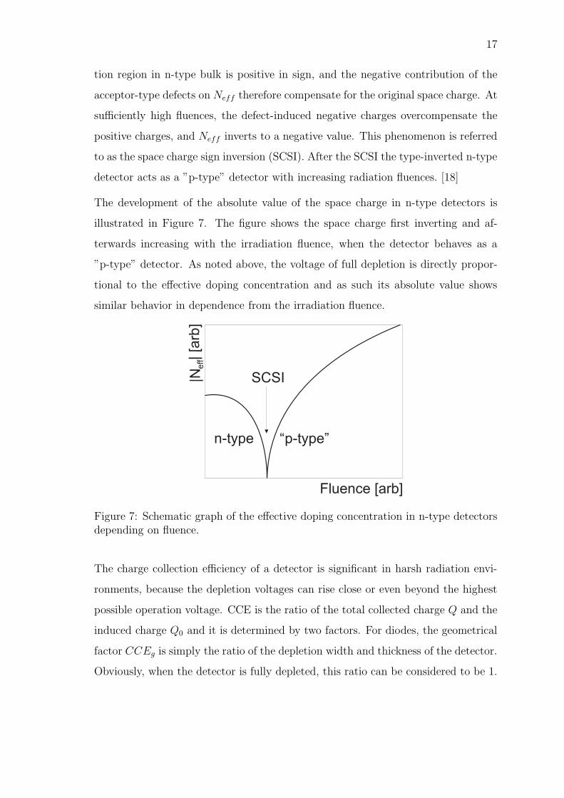
17
tion region in n-type bulk is positive in sign, and the negative contribution of the
acceptor-type defects on Neff therefore compensate for the original space charge. At
sufficiently high fluences, the defect-induced negative charges overcompensate the
positive charges, and Neff inverts to a negative value. This phenomenon is referred
to as the space charge sign inversion (SCSI). After the SCSI the type-inverted n-type
detector acts as a ”p-type” detector with increasing radiation fluences. [18]
The development of the absolute value of the space charge in n-type detectors is
illustrated in Figure 7. The figure shows the space charge first inverting and af-
terwards increasing with the irradiation fluence, when the detector behaves as a
”p-type” detector. As noted above, the voltage of full depletion is directly propor-
tional to the effective doping concentration and as such its absolute value shows
similar behavior in dependence from the irradiation fluence.
SCSI
n-type “p-type”
Fluence [arb]
|Neff| [a
rb]
Figure 7: Schematic graph of the effective doping concentration in n-type detectorsdepending on fluence.
The charge collection efficiency of a detector is significant in harsh radiation envi-
ronments, because the depletion voltages can rise close or even beyond the highest
possible operation voltage. CCE is the ratio of the total collected charge Q and the
induced charge Q0 and it is determined by two factors. For diodes, the geometrical
factor CCEg is simply the ratio of the depletion width and thickness of the detector.
Obviously, when the detector is fully depleted, this ratio can be considered to be 1.
18
As mentioned above, radiation damages cause trapping of charge carriers in deep
level states in the detecting volume. Let the trapping induced factor be CCEt, and
thus [20]
CCE =Q
Q0
= CCEg · CCEt =W
D
τeff
tdr
·
(
1 − e−
tdrτeff
)
(20)
results for CCE. W is the depletion width of the p-n junction and D the detector
thickness. The drifting time and effective trapping time of the charge carriers are
denoted with tdr and τeff , respectively. The effective trapping time equals the
generation lifetime in Equation 16 and can be written as [21]:
τeff =1
σe,hvtNt
, (21)
where Nt is the the density of deep levels and vt is the thermal velocity. The
trapping cross section is denoted by σe,h, which determines the tendency of the
charge carriers to get trapped in deep level states. The detrapping time, on the
other hand, is strongly dependent of temperature [21]:
τdetrap =1
σe,hvtNC,V e−
EtkBT
. (22)
Here NC,V is the density of states of either the conduction band or the valence
band, depending of the type of the detector bulk, and Et is the activation energy
for detrapping.
3.2 Methods for the Improvement of Radiation Hardness
It is possible to use three different approaches to develop more radiation hard detec-
tors. Adding impurity atoms to the semiconductor material on purpose to enhance
the radiation hardness is called defect engineering. In addition, device engineering
methods can be employed and the operational conditions of the detectors can be var-
ied. For example, the CERN RD39 collaboration emphasizes research in cryogenic
operation temperatures of silicon detectors [20].
Zheng Li et al. observed [10], that oxygen content improves the radiation hardness
of heavily irradiated silicon. The detailed explanation is that impurity atoms like

19
oxygen or carbon capture microscopic defects. The oxygen atoms react with the
diffusing vacancy defects in the bulk material, forming new complexes of defects
and impurities. Carbon reacts with interstitials; unlike oxygen, however, carbon
does not show any desirable impact on slowing down the increase of Neff . The
CERN RD48 and RD50 collaborations have put extensive effort into research of
properties in radiation hard silicon. For example, diffusion oxygenated Float Zone
silicon was introduced to the HEP community by the RD48 collaboration [22]; as a
result, this material is indeed used in the pixel detectors in CMS and ATLAS.
A reasonable possibility in the category of device engineering is to process the de-
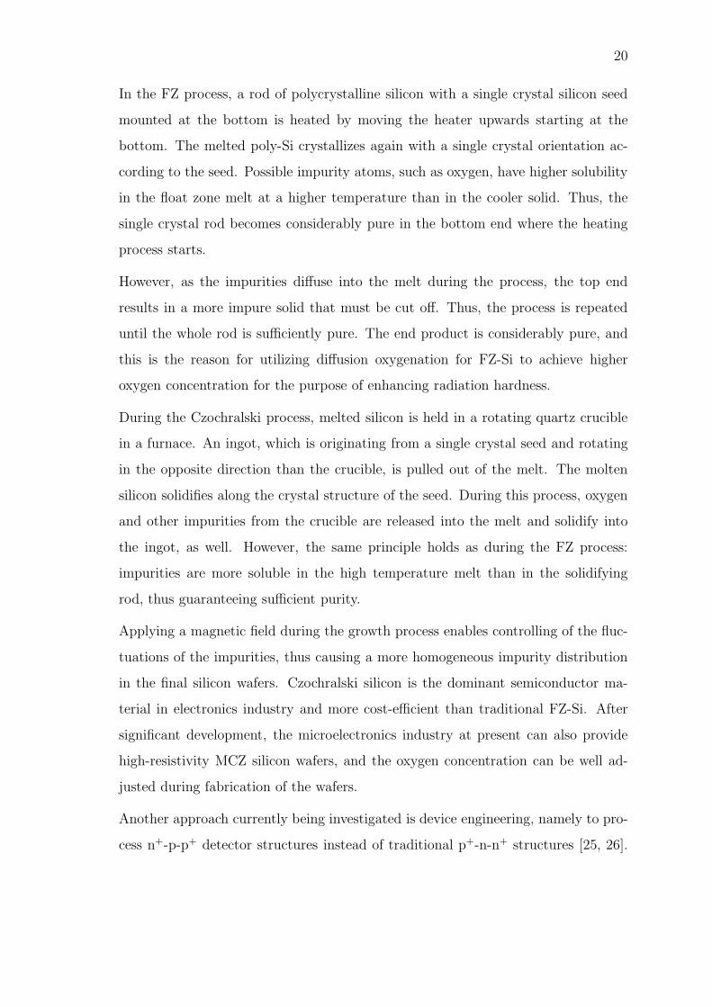
tectors on silicon wafers grown by the magnetic Czochralski method instead of the
FZ method [23, 24]. In both methods sufficient semiconductor purity is achieved via
the higher solubility of impurities at higher temperatures. The essential difference
between the Czochralski and Float Zone methods is the contact to other materials
during crystal growth. In contrast to CZ-Si, FZ-Si never comes in contact with other
materials during the process. A schematic picture of both crystal growth methods
is presented in Figure 8.
Figure 8: Schematic illustration of Float Zone and Czochralski crystal growth tech-niques.
20
In the FZ process, a rod of polycrystalline silicon with a single crystal silicon seed
mounted at the bottom is heated by moving the heater upwards starting at the
bottom. The melted poly-Si crystallizes again with a single crystal orientation ac-
cording to the seed. Possible impurity atoms, such as oxygen, have higher solubility
in the float zone melt at a higher temperature than in the cooler solid. Thus, the
single crystal rod becomes considerably pure in the bottom end where the heating
process starts.
However, as the impurities diffuse into the melt during the process, the top end
results in a more impure solid that must be cut off. Thus, the process is repeated
until the whole rod is sufficiently pure. The end product is considerably pure, and
this is the reason for utilizing diffusion oxygenation for FZ-Si to achieve higher
oxygen concentration for the purpose of enhancing radiation hardness.
During the Czochralski process, melted silicon is held in a rotating quartz crucible
in a furnace. An ingot, which is originating from a single crystal seed and rotating
in the opposite direction than the crucible, is pulled out of the melt. The molten
silicon solidifies along the crystal structure of the seed. During this process, oxygen
and other impurities from the crucible are released into the melt and solidify into
the ingot, as well. However, the same principle holds as during the FZ process:
impurities are more soluble in the high temperature melt than in the solidifying
rod, thus guaranteeing sufficient purity.
Applying a magnetic field during the growth process enables controlling of the fluc-
tuations of the impurities, thus causing a more homogeneous impurity distribution
in the final silicon wafers. Czochralski silicon is the dominant semiconductor ma-
terial in electronics industry and more cost-efficient than traditional FZ-Si. After
significant development, the microelectronics industry at present can also provide
high-resistivity MCZ silicon wafers, and the oxygen concentration can be well ad-
justed during fabrication of the wafers.
Another approach currently being investigated is device engineering, namely to pro-
cess n+-p-p+ detector structures instead of traditional p+-n-n+ structures [25, 26].

21
The p-type detectors show comparable electrical properties to those of n-type detec-
tors. Furthermore, the behavior of the full depletion voltage has been observed to
be less sensitive to harsh irradiation [25]. In addition, in such a detector, the signal
is read from the n+-type implantation; i.e., the charge carriers contributing to the
signal are electrons. Electrons have a drift time of approximately 10 ns through a
300-µm detector. This is more than twice as fast as the drift time of holes in n-type
detectors; i.e., the mobility of electrons is significantly higher than that of holes. In
addition, electrons have lower trapping probability than holes; this leads to higher
charge collection efficiency, as well.
A significant difference between n-type and p-type bulk is the occurrence of space
charge sign inversion. In contrast to n-type, p-type detectors do not show a tendency
to SCSI that was explained in Section 3.1. Thus, the p-n junction remains close to
the read-out electrode in the p-type case, and this leads to a desirable effect that
relates to signal quality. The electric field in real segmented and heavily irradiated
detectors is not linear as that through an ideal diode [27]. The geometry of a
detector determines the weighting of the electric field [28]. The weighting field effect
causes the charge carriers to induce most charge close to the segmented side of
the detector and in the corresponding read-out contact. As the collected charge
consists of electrons with the advantages described above, using n+-p-p+ structures
can result in higher charge collection.
The closer the strong electric field is to the segmented side of the detector, the better
the signal is localized. This is a clear advantage, as the silicon detectors are mainly
used in tracking systems. Consequently, it is profitable to have the p-n junction and
thus the strongest electric field close to the n+-read-out electrode.
The shape of the electric field provides information about both the space charge
of the bulk as well as the behavior of the charge carriers. These, in turn, have an
impact on practically all the parameters for radiation hardness. Thus, it can be
concluded, that it is of importance to analyze the electric field of silicon detector
structures in radiation hardness studies.
22
3.3 Annealing
The irradiated silicon detectors are very sensitive to heat treatment. After a long-
time exposure to room temperature, or at sufficiently high temperatures, the micro-
scopic defects are annealed in the crystal. The annealing mechanisms are migration,
complex formation and complex dissociation of the defects [18].
It has been observed, that annealing during a relatively short time has radiation
hardness improving effects, whereas relatively long-term annealing impairs the ra-
diation hardness of detectors. Therefore, the effects of heat treatment are divided
into two categories: beneficial and reverse annealing. Both of these annealing types
depend on the irradiation fluence, annealing time, and annealing temperature. Pre-
vious studies [18] have shown that exposure of irradiated silicon detectors to room
temperature for 55 h corresponds roughly to the exposure of the detectors to 80 for
2 min in the range of beneficial annealing. For reverse annealing, 2 min at 80 ap-
proximately correspond to 10 days at room temperature.
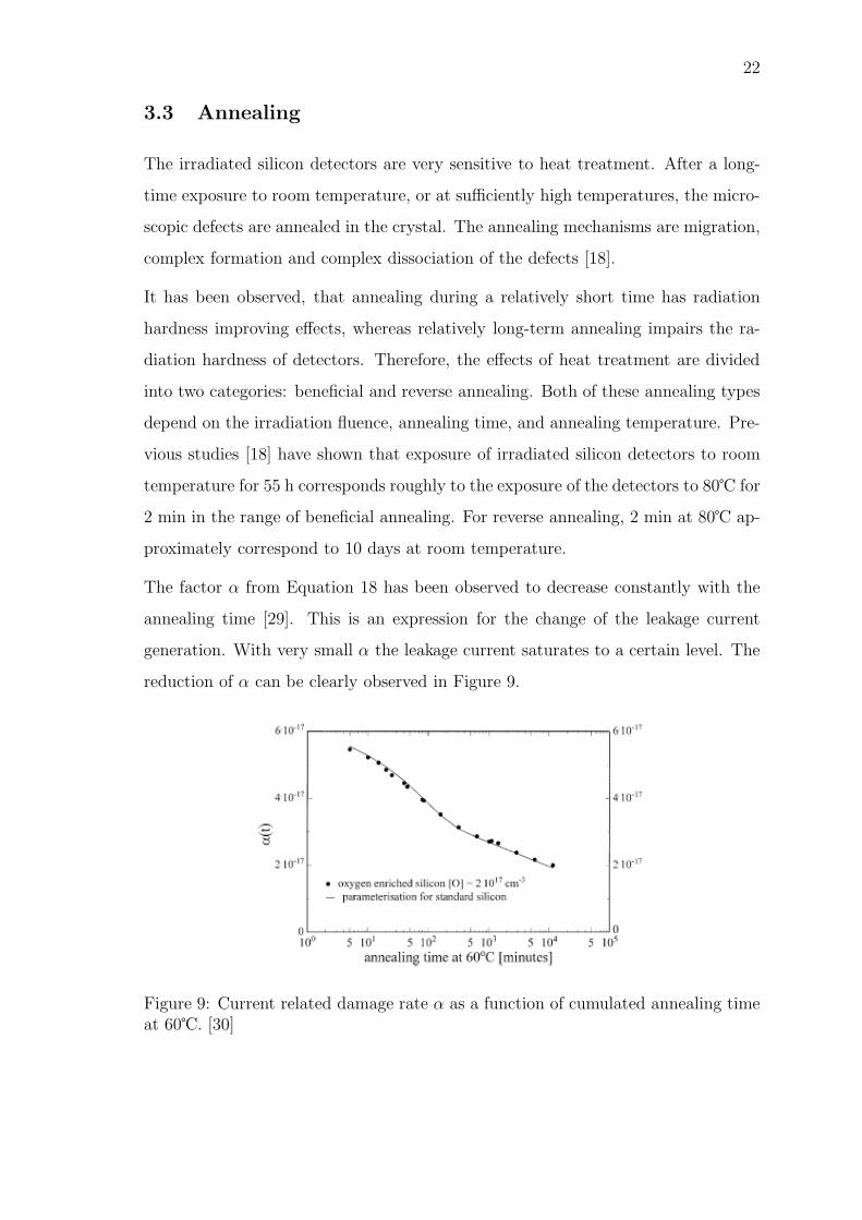
The factor α from Equation 18 has been observed to decrease constantly with the
annealing time [29]. This is an expression for the change of the leakage current
generation. With very small α the leakage current saturates to a certain level. The
reduction of α can be clearly observed in Figure 9.
Figure 9: Current related damage rate α as a function of cumulated annealing timeat 60. [30]

23
On the other hand, observations have been made of decreasing depletion voltages
during the first phase of annealing followed by an increase of the Vfd absolute values
in the second phase. This behavior has also lead to the terms of beneficial and reverse
annealing. As described in Section 3.1, the changes in the depletion voltages depend
on the changes of the effective doping concentrations. The change ∆Neff is a sum
of three components. In addition to the completely fluence dependent component,
the components describing beneficial and reverse annealing are significant, as well.
The behavior of ∆Neff is illustrated in Figure 10.
Figure 10: Change of effective doping concentration ∆Neff during isothermal an-nealing at 60 of oxygen enriched silicon detectors irradiated with different neutronfluences. [30]
Creation of acceptor-type defect complexes can be used as an explanation for the
increase of |Neff | and |Vfd|, which becomes evident especially during reverse an-
nealing. During beneficial annealing, however, the acceptor type crystal defects are
annealed. According to Equation 11, the effective doping concentration is the differ-
ence between the donor and the acceptor concentration. A majority of acceptor-type
charge density, as in p-type devices, results in a negative effective doping concen-
tration. With the annealing of the acceptors, Neff becomes less negative in p-type
detectors. Consequently, the absolute value of the depletion voltage decreases with

24
the reduction of |Neff |. The same phenomenon of beneficial annealing can be ob-
served in n-type detectors after space charge sign inversion.

25
4 Transient Current Technique Measurements
Analog to detector operation, bias voltage is applied during TCT measurements.
The principle of TCT measurements is to observe the signal created by drifting
charge carriers in the silicon detector bulk. The free charge carriers are generated
in consequence of illuminating the detector by red laser light. If the front side
implantation of the reverse-biased diode is illuminated, the charge carriers, that are
collected from the front side, drift to the contact faster than the read-out electronics
can respond. On the other hand, the carriers opposite in sign drift through the
whole detector to the back side. This transient current is the measured signal.
Figure 11: a) The back side of a n+-p−-p+ diode is being illuminated, and theresulting TCT signal comes from electrons. b) Illumination of the front side of thesame diode structure results in a TCT signal caused by holes.
If a reverse-biased detector is being illuminated from the front side, the measured
signal originates from the charge carriers equal in sign to the majority carriers in the
bulk as presented in Figure 11. The figure shows how the TCT signal in a p-type
detector is caused by holes when illuminated from the front side. Illumination from
the back side results in a signal originating from electrons.
It is possible to extract the response of the detector to MIP’s by performing TCT
measurements on diodes illuminated by infra red lasers. Photons with a wavelength
26
in the infra red region have an energy lower than the band gap of silicon. Thus,
the IR photons penetrate considerably deeper into the 300-µm detector bulk than
photons in the red wavelength region. As as result, the generation of e-h pairs
remains moderate but homogeneous through the entire bulk. This leads to a TCT
signal caused by both charge carriers, electrons and holes, as is the case with real
MIP’s.
The benefits of TCT measurements with IR illumination become evident in the
determination of Vfd and CCE. More reliable determination of the state of full
depletion is possible, when the charge carriers are generated homogeneously through
the device. Otherwise, with the possibility of maximum carrier densities close to
the electric field maximum, the majority of charge carriers could be collected before
the whole detector is depleted.
The MIP simulation is advantageous when considering examination of the charge
collection efficiency, as well. As mentioned in Section 3.1, CCE is the relation of
the collected charge Q and the originally induced charge Q0 in a detector. With the
infra-red TCT measurements, Q0 can be set equivalent with the collected charge in
a non-irradiated detector, i.e., CCE = 1. This is assumed to correspond to 22000
electrons induced by a single MIP in a 300-µm thick silicon detector.
4.1 Determination of the Electric Field Distribution,
Full Depletion Voltage, and Effective Trapping Time
According to Ohm’s Law the transient current is directly dependent on the electric
field between the front and back side of the detector:
~J = σ · ~E. (23)
~J is the current density, σ the conductivity, and ~E the electric field. As mentioned
previously, the diffusion component caused by the carrier concentration gradient
can be neglected when considering TCT measurements. Thus, the drift current is
dominant, and the current density in Equation 23 can be written for electrons and

27
holes as follows [13]:
Jn = qµnnE, (24)
Jp = qµppE. (25)
Here, q is the elementary charge, n the charge concentration of electrons and p
that of holes. The mobilities for electrons and holes are denoted by µn and µp,
respectively.
From this follows that the shape of the TCT signal resembles the shape and location
of the electric field. The electric field is strongest at the location of the actual p-n
junction. There, the drift current is at its highest, as well, since it is proportional
to the electric field as can be seen in the equations above. The junction is usually
located at the interface of the bulk and the implantation opposite in sign. If the
signal is measured from the side where the junction is located, the TCT signal is
descending. If the junction has moved to the back because of space charge sign
inversion, the measured signal from the front side is ascending. This is illustrated in
Figure 12. A clear sign of SCSI is thus an ascending TCT signal as in Figure 12b).
Obviously, this leads to conclusions about the sign of the space charge, as well, when
the junction structure of the detector is known.
In addition to the determination of the sign of the space charge and the electric
field distribution, it is also possible to extract the full depletion voltage Vfd and
the effective trapping time τeff in the bulk from the TCT measurement data. The
transient current measurement allows to obtain directly the amount of collected
charge by integrating the current signal over time. The charge collection also rises
steeply at increasing voltages until the full depletion voltage.
If trapping and detrapping of the charge carriers occur within the current integration
time, the amount of collected charge saturates at voltages above Vfd, e.g., at full
depletion. If the shaping time of the read-out electronics is as short as in the LHC
experiments, detrapping of the captured charge carriers does not occur within the
RC time constant of the read-out. Thus the total induced charge is not collected,
and the saturation of the charge collection does not become visible in a charge
28
Figure 12: a) A p+-n-n+ structure with the maximum electric field at front providesa descending transient current. b) A type-inverted p+-n-n+ structure has its electricfield maximum at the back side of the diode, and the transient current is ascending.
collection measurement graph. Instead, the graph continuously shows increasing
charge collection; however, with a reduced slope at voltages |V | > |Vfd|. [31]
The value of the depletion voltage can be determined by a graphical method from a
graph showing the collected charge as a function of applied bias voltage as illustrated
in Figure 13. The intersection of the linear fittings of the high and small slope regions
provide the voltage of full depletion.
The method for the determination of the effective trapping time τeff is presented in
the following according to [31]. The transient current i(t) in the detector caused by

29
CC
E[a
rb]
Voltage [arb]
CCE Graph
Vfd
Figure 13: Obtaining Vfd from a CCE graph.
one charge carrier can be expressed with the help of Ramo’s theorem [32]:
i(t) = qvdrEv = qµE(x)1
D, (26)
where q is the elementary charge, vdr the velocity of the charge carrier and Ev is the
electric field caused by unit potential in the location of the carrier. The right hand
side of the equation introduces the carrier velocity as a product of carrier mobility
µ and electric field E(x). Ev is replaced by the inverse value of the thickness D of
a non-segmented pad detector, i.e., a diode.
When considering the total transient current I(t), the carrier concentration factor
must be added to Equation 26. The carrier concentration, however, does not hold
the constant value of injected carriers but decreases depending on τeff [31]. The
dependence for the electron concentration n is written as:
n = n0 · e−
tdrτeff , (27)
where n0 is the injected carrier density, and tdr is the drift time of the carriers
through the diode. The exponential term above can be used to correct the measured

30
transient current, and I(t) results in:
I(t) = n0
qµE(x)
De−
tτeff . (28)
This expression for the transient current indeed equals the current that can be
deducted from the current density in Ohm’s law (Equations 24, 25), except for the
exponential correction added due to trapping.
The collected charge can be calculated by integrating the transient current over
time:
Q =
∫ tdr
0
I(t)dt (29)
=Q0vdr
D
∫ tdr
0
e−
tτeff dt
=Q0vdr
Dτeff
(
1 − e−
tdrτeff
)
=Q0W
D
τeff
tdr
(
1 − e−
tdrτeff
)
. (30)
Here, the depletion width W results from vdrtdr. It has also been assumed that
the electric field through the non-segmented pad-detector is constant, thus causing
the transient current to remain independent of location x. When dividing equa-
tion 30 by Q0, the result is indeed the charge collection efficiency as demonstrated
in Equation 20.
Let us assume, that the charge collection efficiency depends only on the trapping
factor at full depletion of the detector as the depletion width W equals the device
thickness D. Then, with the right value for τeff inserted in the current integral, the
corrected amount of collected charge stays constant for voltages above Vfd. Hence,
searching a value, that forces the charge collection graph to reach a plateau typical
for saturation, results in an accurate value for the effective trapping probability.
Equation 30 can be used to evaluate τeff with the collected charge Q being the
integral over time of the measured current transient. If the detectors have been
irradiated with a modest particle fluence (< 2 · 1015 neq/cm2), the effective trapping
time has a significantly larger value than the drift time of the charge carriers (τeff ≫

31
tdr). Thus following approximation of Equation 30 becomes valid for the collected
electrons [20]:
Q ≈ Q0
W
D(1 −
1
2·τeff
tdr
). (31)
After extremely high radiation (∼ 1016 neq/cm2) or long time annealing, the effective
trapping time is considerably shorter than the drifting time through the device, and
the charge carriers are captured in traps within the measurement time window.
Under such conditions (τeff ≪ tdr), Equation 30 for electrons simplifies to [20]
Q ≈ Q0
W
D
τeff
tdr
. (32)
4.2 Measurement setup
The TCT measurement setup used in this thesis project was designed and built by
the CERN RD39 Collaboration [33]. A schematic overview of the setup is presented
in Figure 14, and a photograph of the practical measurement equipment is shown
in Figure 15. The sample is placed on a cold finger inside a vacuum chamber. The
vacuum is created with a turbo pump and a Leybold helium stirling cooler is used for
the cooling of the chamber. The bias voltage from a source meter unit is applied to
the sample diode through a coaxial copper transmission line designed for cryogenic
applications in particular.
The diodes are mounted with carbon adhesive tapes on ceramic plates. The contact
between the diode and the transmission line is realized by soldering a gold pin from
the back side of the ceramic plate into an opening in the middle of the plate. This pin
can be directly connected to the coaxial cable. The ceramic plates have a patterned
gold metallization, and the pad contact on the front side of the sample diode along
with the guard ring are bonded to the metallization. The contact between the
gold-plating and the copper cold finger is established by four copper springs.
As the back sides of the diodes are attached to the plates firmly, only the front side
of the sample can be illuminated with a laser diode from Advanced Laser Diode

32
Figure 14: Sketch of the principle of the TCT measurement setup.
Systems A.L.S. GmbH. The used wavelengths are in the red region (678 nm) and
infra-red region (1060 nm), and the pulse length of the lasers is about 30 ps. The
laser diodes were operated in all measurements with a trigger rate of 50 Hz and
an output efficiency of 70% with the maximum optical power being 250 mW. The
same trigger rate was also used for triggering the Le Croy Wavepro 7K 3 GHz
oscilloscope, which reads out the output signal. The output signal is transmitted to
the oscilloscope over the same coaxial cable as the bias voltage and amplified before
the plug-in. The gain is 600, and the impedance of the oscilloscope equals 50 Ω.
The measurement settings and data aquisition are handled by a user interface based
on LabView.
4.3 Samples and Measurements
This study covered the examination of altogether 11 different diodes. The diodes
have a basic double-sided p+-n-n+ or n+-p-p+ pn-diode structure. The component
area is surrounded with a guard ring to define the active volume precisely and prevent
skewing of the leakage current measurements. With no guard ring, the electric field
could reach the dicing edge of the sample. Then, large external currents could be
pulled into the diode.
The contact pad on the front side has an opening in the middle, thus enabling direct

33
Figure 15: The TCT measurement setup of the CERN RD39 Collaboration.
illumination of the diode. The opening in the pad, the guard ring, and the bonding
wires can be seen in Figure 16a), where a diode is glued on the ceramic plate. The
size of the diode samples is 8 mm x 8 mm, although the active detecting volume is
sized 5 mm x 5 mm. Figure 16b) is a photograph of a processing mask of the diodes,
which shows the pad contact on the front side of the diode as well as the guard ring
located between the active detector and the edge of the sample.
a) b)
Figure 16: a) A diode sample on a ceramic plate prepared for TCT measurements.b) Photograph of a corner in the processing mask. The pad contact opening andthe guard rings are clearly visible.

34
The experiments included investigation of both Float Zone silicon samples and mag-
netic Czochralski silicon samples. The FZ diodes have been fabricated at Centro
Nacional de Microelectronica (IMB-CNM, CSIC) in Barcelona, Spain. They have
been provided by the CERN RD50 Collaboration. The MCZ diodes have been man-
ufactured in the clean room facilities of TKK Micronova in Espoo, Finland. All
three FZ-Si diodes were processed from n-type bulk. On the other hand, p-type as
well as n-type bulk were represented among the MCZ-Si diodes. Four diodes of each
MCZ type as well as the three FZ diodes were exposed to different doses of proton
radiation. The energy of the protons equaled 23 GeV. The irradiation was carried
out at the CERN Proton Synchrotron (PS). Table 1 presents the different radiation
fluences and the according samples.
Table 1: The proton irradiation fluences, the neutron equivalent doses, and corre-sponding sample names.
Fluence Fluence MCZ n-type MCZ p-type FZ n-type[23 GeV p/cm2] [1 MeV n/cm2]1.6 · 1014 9.92 · 1013 n-61 p-50 F-329.7 · 1014 6.014 · 1014 n-58 p-55 F-421.3 · 1015 8.06 · 1014 n-57 p-57 F-702.4 · 1015 1.488 · 1015 n-56 p-61 F-81
Three different measurements at two temperatures were performed on all samples.
Before the start of the cooling, the pressure in the vacuum chamber was pumped
down to at least 1.0 · 10−3 mbar. First, TCT measurements were carried out at
240 K under illumination by the infra-red laser. The scanned bias voltage range
covered voltages from zero to 500 V with a step size of 25 V.
If the collected charge saturated within the scanned voltage range, the value for
the full depletion voltage Vfd was obtained from the charge collection efficiency
graph as shown in Figure 13. A similar measurement was completed with a laser
in the red light region at temperatures 220 K and 240 K. The extracted depletion
voltage was used as a set point approximately in the middle to adjust the voltage
range accordingly. In addition, current-voltage measurements were executed at both
temperatures.

35
After examination of all samples, the n- and p-type MCZ samples with the irra-
diation dose of 9.7 · 1014 p/cm2 were chosen for a further annealing experiment.
Also the behavior of the FZ sample with the dose 1.3 · 1015 p/cm2 after annealing
was examined for comparison. The annealing experiment included the annealing of
the samples at 80. Each of these samples was annealed separately in six steps.
The variable in these steps was the annealing time according to the recursive rule
tn+1 = 2tn with n running from 1 to 6 and annealing time t1 for the first annealing
step being 4 minutes. From this follows the accumulated annealing time of 252
minutes for each sample. The cumulative annealing times and those of each step
are summarized in Table 2. After every annealing step, the samples were subjected
to the same TCT and I–V measurements as described above for all diode samples
before annealing.
Table 2: Cumulative annealing times and those of each step.
Annealing times [min]Single step 4 8 16 32 64 128Cumulative 4 12 28 60 124 252

36
5 Results and Discussion
Results from the conducted measurements are organized in the following way. First,
voltages of full depletion are extracted from MIP measurements, and leakage current
values corresponding to the depletion voltages result from I–V measurements. Sec-
ond, the electric field of the diodes is examined with the help of TCT measurements.
At last, annealing behavior of different types of diodes is investigated, as well, with
the aforementioned methods.
In general, the results lead to the conclusion that MCZ-Si diodes withstand both
irradiation as well as annealing better than FZ-Si diodes when judged by parameters,
such as depletion voltage or leakage current. Both types of MCZ based diodes show
more preferable performance at 220 K than at 240 K, as the TCT signal strength, for
example, is generally higher and the leakage currents lower at the lower temperature.
The values resulting for depletion voltages before and after annealing as well as
leakage currents after annealing tend to be lower for the p-type MCZ diode samples
than for the n-type MCZ samples. Low values for these parameters are as well
desired in detector operation in HEP experiments, as well.
5.1 Voltages of Full Depletion and Leakage Currents
The voltages of full depletion Vfd were determined from the TCT measurements
executed under excitation by a 1060-nm laser at 240 K. The graphical method
explained in Section 4.1 was utilized to extract the values for Vfd, if the rise of charge
collection saturated; i.e., the diode was fully depleted, within the scanned voltage
range of 500 V. None of the samples with the highest irradiation dose equivalent
to 1.5 · 1015 1 MeV neq/cm2 was fully depleted at a voltage below 500 V. The
resulting depletion voltages from the measurement are summarized in Table 3.
The absolute values of the depletion voltages are clearly lower in samples processed
from magnetic Czochralski silicon than in float zone diodes. Furthermore, as opposed
to the MCZ samples, the FZ-Si diodes did not deplete at a reverse bias below

37
Table 3: Vfd values in [V] determined at a temperature of 240 K.
Dose [23 GeV p/cm2] MCZ n-type MCZ p-type FZ n-type1.6 · 1014 168.3 -57.2 119.19.7 · 1014 252.3 -197.8 279.01.3 · 1015 310.8 -269.1 n.d.2.4 · 1015 n.d. n.d.
500 V, if they were irradiated with a higher fluence than that corresponding to
6.01 · 1014 1 MeV neq/cm2. The lowest absolute value of the depletion voltage
was determined for the MCZ p-type sample for each irradiation fluence. This is
illustrated in Figure 17, as well.
0 2 4 6 8 10 12 14
x 1014
0
50
100
150
200
250
300
350Full depletion voltage measured at 240 K
Fluence [23 GeV p/cm2]
|Vfd
| [V
]
MCZ n−typeMCZ p−typeFZ n−type
Figure 17: Obtained Vfd values for different diode types in dependence of fluence.
Table 4: Ileak values in [µA] measured at a bias voltage equaling Vfd and a temper-ature of 240 K.
Dose [23 GeV p/cm2] MCZ n-type MCZ p-type FZ n-type1.6 · 1014 -0.162 0.175 -0.3109.7 · 1014 -0.790 0.898 -1.2351.3 · 1015 -1.803 1.505 n.d.2.4 · 1015 n.d. n.d.
The current-voltage measurement at the temperature of 240 K provided the value of
the leakage current at a voltage equaling Vfd. The results are presented in Table 4.
38
While both types of MCZ-Si diodes show similar absolute values for the leakage
current, the values for the FZ-Si diodes are clearly higher than those for the other
samples. This could be expected, as the depletion voltage values for the FZ-Si
samples rose clearly above those of the MCZ-Si samples.
5.2 TCT Characterization
TCT measurements were performed on all samples (see Table 1) under illumination
of a red (λ = 678 nm) laser. The results for each diode type with different irradiation
fluences are presented in the following. The TCT signals are measured from fully
depleted diodes. If the diodes did not deplete at a voltage smaller than 500 V, the
signal at a bias voltage of 500 V is shown. A comparison of the MCZ and FZ samples
is also included at the end of this section.
TCT signals measured from fully depleted n-type and p-type MCZ-Si diodes can
be seen in Figures 18 and 19, respectively. Visual inspection reveals for the n-type
samples a better signal to noise ratio (SNR) than for the p-type samples. In principle,
the widths of the signals show the drifting time of the charge carriers through the
device bulk. Typical values for drifting times through a standard 300-µm silicon
device are about 10 ns for electrons and 25 ns for holes. The signal widths of the
detectors irradiated with the smallest fluence stay clearly below these values both
for electrons in the n-type diode as well as for the holes in the p-type sample.
Furthermore, with increasing irradiation dose, the signals become more narrow as
can be seen in the figures. The difference in width between the the widest and most
narrow peaks is 2–3 ns for the n-type samples at both temperatures. The difference
is approximately 7 ns for the p-type samples, although the difference seems lower at
220 K than at 240 K.
The reason for the narrow signals is that the trapping probability in a silicon detec-
tor increases with the radiation exposure. Thus, the charge carriers travelling the
longest distance through the device get trapped before reaching the read-out. This
results in a smaller signal width.

39
0 0.5 1 1.5
x 10−8
0
0.2
0.4
0.6
0.8
1
1.2
1.4
Time [s]
TC
T S
igan
al [V
]
240 K
0 0.5 1 1.5
x 10−8
0
0.2
0.4
0.6
0.8
1
1.2
1.4220 K
Time [s]T
CT
Sig
anl [
V]
n61 270 Vn58 350 Vn57 425 Vn56 500 V
n61 270 Vn58 350 Vn57 425 Vn56 500 V
Figure 18: TCT signals of the n-type MCZ-Si samples at a voltage V ≈ Vfd + 100Vor, if Vfd ≥ 500V , V = 500V .
0 0.5 1 1.5 2
x 10−8
0
0.05
0.1
0.15
0.2
0.25
0.3
Time [s]
TC
T S
igna
l [V
]
240 K
0 0.5 1 1.5 2
x 10−8
0
0.05
0.1
0.15
0.2
0.25
0.3220 K
Time [s]
TC
T S
igna
l [V
]
p60 500 Vp57 375 Vp55 300 Vp50 150 V
p60 500 Vp57 375 Vp55 300 Vp50 150 V
Figure 19: TCT signals of the p-type MCZ-Si samples at a voltage V ≈ Vfd + 100Vor, if Vfd ≥ 500V , V = 500V .

40
The TCT signals measured at 220 K are generally more narrow than those measured
at 240 K. This can be explained by the electron and hole mobilities that depend
strongly on temperature. Decreasing the measurement temperature by 20 K results
in higher mobilities for both electrons and holes. As a result, the charge carriers are
collected faster and the signal width decreases.
Another effect caused by trapping can be observed in the signal shapes. MCZ-
Si detectors with n-type bulk usually experience SCSI at a fluence in the order
of magnitude of 1014 1 MeV neq/cm2. Thus, after sufficient irradiation, the TCT
signals should change their shape from descending to ascending according to the
electric field distribution. However, our results show only descending signals. It can
be assumed for the samples with the higher irradiation fluences, that the trapping
has narrowed the signals to an extent, when the ascending part of the signal, and
thus the location of the shifted p-n junction, is not visible anymore.
0 0.5 1 1.5
x 10−8
0
0.2
0.4
0.6
0.8
1
1.2
Time [s]
TC
T S
igna
l [V
]
240 K
0 0.5 1 1.5
x 10−8
0
0.2
0.4
0.6
0.8
1
1.2220 K
Time [s]
TC
T S
igna
l [V
]
F32 220 VF42 375 VF70 500 V
F32 220 VF42 375 VF70 500 V
Figure 20: TCT signals of the FZ-Si samples at a voltage V ≈ Vfd + 100V or, ifVfd ≥ 500V , V = 500V .
Figure 20 illustrates the TCT signals measured from the n-type FZ-Si diodes. Mea-
surements of sample F-32 (1.6 · 1014 23 GeV p/cm2), which has been exposed to the

41
smallest irradiation dose, result in a shifted peak compared to all other measurement
results presented in this study. This may be caused by the SCSI induced already
after lower fluences of irradiation. The double peak effect can be clearly observed in
the highly irradiated sample F-70 (1.3 · 1015 23 GeV p/cm2) at 220 K. Double-peak
formation is caused by trapping of the charge carriers in deep energy levels of the
silicon bulk and has been explained in detail in [27].
An obvious discrepancy in the measurements presented in Figure 20 is the very low
relative signal amplitude of the sample F-42 (9.7 · 1014 23 GeV p/cm2). The weak,
nearly shapeless signal is possibly the result of the optical properties of the diode
that differ from the other samples. The refraction index of the surface at the opening
for the laser might be different.
The weak signal could be caused by physical damage of the sample, as well. Namely,
the soldering of the gold pin to the diode was observed to be damaged during the
measurements. As the pin is the connector between the sample and the signal
transmission line, it is plausible that the signal read out on the oscilloscope was
influenced by the defect signal transmission.
It is possible to make some deductions from the measurement results of sample F-
42, nonetheless. Figures 21 and 22 present the collected charge as a function of
bias voltage for samples F-32 and F-42, respectively. The charge collection curve in
Figure 21 is typical for FZ diodes that have undergone space charge sign inversion.
The charge collection remains low at low bias voltages, as the maximum electric field
has shifted to the back side of the diode while the red laser creates most carriers
close to the front side. However, when the voltage reaches a sufficiently high value,
the charge is collected from the back side, as well.
Figure 22, on the other hand, shows similar tendencies with regard to the shape of
the charge collection graph. Thus, it seems that SCSI has occurred in sample F-42.
However, the maximum bias voltage of 500 V may not be sufficient to enable charge
collection from the back side.
In Figure 23, TCT signals from all sample types are compared that have been

42
0 50 100 150 200 2500
0.2
0.4
0.6
0.8
1
1.2x 10
−10 Sample F−32, Dose 1.6 x 10 14 23 GeV p/cm 2
Voltage [V]
Col
lect
ed c
harg
e [C
]
220 K240 K
Figure 21: Charge collection in sample F-32 under red-laser illumination.
0 100 200 300 400 5000
1
2
3
x 10−11
Voltage [V]
Col
lect
ed c
harg
e [C
]
Sample F−42, Dose 9.7 x 10 14 23 GeV p/cm 2
220 K240 K
Figure 22: Charge collection in sample F-42 under red-laser illumination.

43
exposed to an irradiation dose of 1.3 · 1015 23 GeV p/cm2. The amplitudes of the
signals are scaled to a mutual, arbitrary maximum to simplify the comparison of
the signal shapes. While both types of MCZ-Si diodes show very similar descending
signal shapes at both temperatures, the shape of the n-type FZ diode is clearly
ascending at 240 K, thus indicating SCSI. The signal shape of the FZ diode at
220 K delivers proof of double-peak formation in the electric field of the device.
0 0.5 1 1.5
x 10−8
0
0.1
0.2
0.3
0.4
0.5
0.6
0.7
0.8
0.9
Time [s]
TC
T s
igna
l [ar
b]
220 K
0 0.5 1 1.5
x 10−8
0
0.1
0.2
0.3
0.4
0.5
0.6
0.7
0.8
0.9240 K
Time [s]
TC
T S
igna
l [ar
b]
FZ n−typeMCZ n−typeMCZ p−type
FZ n−typeMCZ n−typeMCZ p−type
Figure 23: Comparison of diodes processed on different wafers. TCT signalvalues are scaled to a mutual maximum. Irradiation fluence on the samples:1.3 · 1015 23 GeV p/cm2.
The signal forms of the FZ diode can be explained by trapping in certain radiation
induced defects. At 240 K, charge carriers get trapped and detrapped within the
time corresponding to the laser trigger rate of the TCT setup. Thus, the defects
contribute to the effective space charge, which leads to SCSI and one electric field
maximum on the back side of the diode.
Lowering the temperature to 220 K raises the time the carriers stay captured to a
higher value than that resulting from the laser trigger rate. Thus the defects do
not contribute to the effective space charge any longer. The peak on the left rises

44
indicating another electric field maximum at the front side of the diode. In addition,
it can be assumed that the aforementioned defects react with oxygen, as double-peak
formation can be observed in neither type of MCZ diodes.
5.3 Annealing Experiment
The samples irradiated with a dose of 9.7 · 1014 23 GeV p/cm2, i.e., samples n-58, p-
55, and F-70, were annealed at 80. The voltages of full depletion were determined
at 240 K after each annealing step by the method explained in Section 4.1. The
results for the depletion voltages in dependence of the cumulative annealing time
are presented in Table 5 and Figure 24.
The shortest annealing time of 4 minutes caused the depletion voltage of the FZ
diode to rise to 375 V. Further annealing raised the depletion voltages above 500 V,
and thus they could not be determined exactly. Therefore, no Vfd values for that
sample are illustrated in the figure. Furthermore, with no information about the
depletion voltage, results for leakage currents or TCT measurements of fully depleted
FZ diodes cannot be given.
Table 5: Vfd in [V] for each annealed sample after respective cumulative annealingtime.
4 min 12 min 28 min 60 min 124 min 252 minn-58 252.3 215.7 205.0 221.1 274.2 349.9p-55 -182.6 -183.2 -177.3 -224.0 -264.7 -320.7F-70 374.9 >500 >500 >500 >500 >500
Both samples of MCZ-Si show characteristic behavior of beneficial annealing as the
depletion voltages decrease with increasing annealing time until a minimum, which
is followed by reverse annealing. The minimum depletion voltage appears for both
diodes after the third annealing step, i.e., cumulative annealing of 28 minutes at
80. This corresponds roughly to one month in room temperature.
As can be seen in Figure 24, the absolute values of the depletion voltages are gen-
erally slightly lower for the p-type than for the n-type samples. For example, the
minimum value of Vfd for sample p-55 equals –177 V, whereas the corresponding

45
value for n-58 is 205 V. The absolute value of Vfd has thus decreased by about
20 V from the value before annealing in sample p-55. The decrease is about 50 V
for sample n-58. The property of beneficial annealing is characteristic for n-type
detectors that have undergone SCSI and p-type detectors, as has been explained in
Section 3.3.
0 50 100 150 200 2500
50
100
150
200
250
300
350
Annealing time [min]
Dep
letio
n vo
ltage
[V]
MCZ n−typeMCZ p−type
Figure 24: Absolute values of depletion voltages after annealing.
Figures 25 and 26 show the leakage currents Ileak in the annealed diodes biased with
a voltage equaling Vfd at the two measurement temperatures 240 K and 220 K.
As can be seen from the figures, the shape of the graphs depicting the evolution
of Ileak values with cumulative annealing time stay similar in the two temperatures
with ∆T = 20K, although the values differ by one order of magnitude. As the
current is strongly temperature dependent, the leakage current results in different
temperatures should not be compared otherwise without scaling them to a reference
temperature.
For both types of detectors, the leakage current decreases during beneficial annealing
and even until after the fourth annealing step. The leakage current in the p-type
sample steadies at both temperatures as expected with regard to previous results.
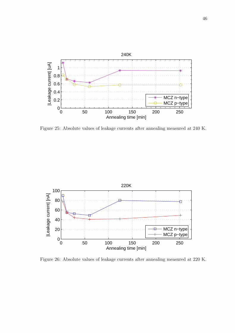
46
0 50 100 150 200 2500
0.2
0.4
0.6
0.8
1
240K
Annealing time [min]
|Lea
kage
cur
rent
| [uA
]
MCZ n−typeMCZ p−type
Figure 25: Absolute values of leakage currents after annealing measured at 240 K.
0 50 100 150 200 2500
20
40
60
80
100220K
Annealing time [min]
|Lea
kage
cur
rent
| [nA
]
MCZ n−typeMCZ p−type
Figure 26: Absolute values of leakage currents after annealing measured at 220 K.

47
However, the Ileak-values at both temperatures start increasing again during the last
two annealing steps.
The depletion voltages for the long-term annealed samples were in general harder
to determine with the used graphical method, as the saturation of the collected
charge shifted close to the maximum bias voltage of 500 V. Naturally, this leads
to inaccuracies in the determination of leakage currents, as well. Furthermore, the
laser operation was not stable during the characterization measurements of the n-
type diode after the second to last annealing step. These factors might have had an
impact on the results, as well.
The response of the MCZ diodes is better at the lower temperature of 220 K through-
out this study. Therefore, TCT signals measured at this temperature are presented
in Figures 27 and 28 to make the influence of annealing on the properties of the
n-type and p-type samples more perceptual.
0 0.5 1 1.5
x 10−8
0
0.2
0.4
0.6
0.8
1
1.2
Sample p55 Dose 9.7x10¹⁴,Measurement at 220 K, Amplitudes scaled
Time [s]
TC
T S
igna
l [ar
b]
No annealingAnnealing step 16 minAnnealing step 32 minAnnealing step 128 min
Figure 27: Fully depleted (V ≈ Vfd + 100V ), annealed MCZ p-type diode measuredat 220 K.
As the differences in signal intensity were small in the p-type detector, save the

48
measurement after the last annealing step, the chosen amplitudes for Figure 27 are
scaled to 1 with the purpose of easier comparison. It is evident from the figure that
the signal shape changes mostly by narrowing after annealing, while the general form
shows no great changes. Annealing narrows the signal in a similar manner as high
irradiation fluence, as the charge collection efficiency degrades because of trapping.
Sample n-58, on the other hand, is affected differently by annealing. While the signal
width remains approximately constant until the second to last annealing step, the
signal shape changes clearly from descending to ascending between the third and
fourth steps. The ascending signal shape is clear evidence for SCSI. This conclusion
holds, even if the SCSI has started earlier, as discussed before. In such a case, the
inversion to an ascending signal can be interpreted as sufficient excess of acceptor
type doping to make the shifted junction asymmetrical enough to be visible in the
TCT measurement despite of trapping. After the last annealing step and total
annealing time of 252 minutes, the signal becomes more narrow, as well, because
trapping hinders reading out the full generated signal.
0 5 10 150
0.1
0.2
0.3
0.4
0.5
0.6
0.7
0.8
0.9
1
Time [ns]
TC
T s
igna
l [V
]
Sample n58 Dose 9.70x10¹⁴
No AnnealingAnnealing step 4 minAnnealing step 8 minAnnealing step 16 minAnnealing step 32 minAnnealing step 64 minAnnealing step 128 min
Figure 28: Fully depleted (V ≈ Vfd + 100V ), annealed MCZ n-type diode measuredat 220 K.

49
6 Summary
This thesis investigated properties of silicon particle detectors by means of the tran-
sient current technique. The TCT measurements were conducted on different types
of sample diodes. Diodes were compared that had been processed on wafers fabri-
cated by the magnetic Czochralski method and by the float zone method. Differences
between n-type and p-type MCZ diodes were examined, as well.
The sample diodes were characterized via parameters obtained from the measure-
ments: voltage of full depletion, leakage current, and charge collection. The dis-
tribution of the electric field in the diode structures was examined qualitatively, as
well. Additionally, the annealing behavior of different detector types was investi-
gated after heat treatment at 80.
It was found, that MCZ-Si diodes withstand both irradiation as well as annealing
better than FZ-Si diodes when judged by parameters, such as depletion voltage
or leakage current. Comparison of collected data from n-type and p-type MCZ-Si
diodes succeeded, as well. The results were supporting the presumption that it may
be possible to use n+-p-p+ structures for future particle detector applications in high
energy physics experiments.
In this study, the p-type samples seemed less sensitive than the n-type samples
to both irradiation as well as annealing, thus indicating advanced radiation hard
properties. It is also possible to make one-sided detector structures of p-type bulk,
as the read-out electronics are preferably connected to the n-type implantation on
the front side of the detectors. The material properties found in this thesis as well as
practical electronic aspects make p-type MCZ-Si attractive for detector applications
in HEP experiments.
Not only the current silicon detectors in the LHC experiments are to be replaced in
the coming years. The next level, the Super-LHC (S-LHC) with even higher collision
rates, has already been planned to start in 10 to 15 years. The decisions have not yet
been made concerning the tracker detectors and their final realization in the S-LHC.

50
Therefore, various studies are being carried out to enhance radiation hardness and
suitability of silicon particle detectors for particle accelerator experiments.
For example, overcoming the problem of trapping, that reduces CCE, has been
investigated within the CERN RD39 Collaboration. As the depletion voltages of the
detectors reach values close or over the operational limits of the experiments, the
charge collection efficiency becomes more important. One possible solution could
be current injected detectors (CID) operated at a temperature of approximately
220 K. These are practically forward-biased regular detectors taking advantage of
the strong temperature dependence of the detrapping coefficient. As can be seen,
the work to improve radiation hardness of the silicon particle detectors remains
continuously relevant.

51
References
[1] CERN. LHC: Facts and figures. http://public.web.cern.ch/public/en/LHC/Facts-en.html. Referred 2.12.2008.
[2] CERN. Missing Higgs. http://public.web.cern.ch/public/en/Science/Higgs-en.html. Referred 2.12.2008.
[3] CERN. CMS – Physics – Hunting the Higgs boson. http://cms-project-cmsinfo.web.cern.ch/cms-project-cmsinfo/Physics/HuntingHiggs/CMS.html.Referred 2.12.2008.
[4] Michel Della Negra, L. Foa, A. Herve, and Achille Petrilli. CMS physics: Tech-
nical Design Report. Technical Design Report CMS. CERN, Geneva, 2006.
[5] Communication Group. CERN LHC: the guide. faq. frequently asked questions.CERN-Brochure-2008-001-Eng. CERN, Geneva, Jan 2008.
[6] CERN. How the LHC works. http://cms-project-cmsinfo.web.cern.ch/cms-project-cmsinfo/Physics/HuntingHiggs/CMS.html. Referred 9.12.2008.
[7] CERN. CMS – Physics. http://cms-project-cmsinfo.web.cern.ch/cms-project-cmsinfo/Physics/index.html. Referred 9.12.2008.
[8] CERN. CMS detector overview. http://cms-project-cmsinfo.web.cern.ch/cms-project-cmsinfo/Detector/FullDetector/index.html. Referred 9.12.2008.
[9] The CMS tracker: addendum to the Technical Design Report. Technical DesignReport CMS. CERN, Geneva, 2000.
[10] Z. Li et al. Investigation of the oxygen-vacancy (A-center) defect complex profilein neutron irradiated high resistivity silicon junction particle detectors. IEEE
Transactions on Nuclear Science, 39(6):1730–1738, Dec 1992.
[11] G Lindstrom, S Watts, and F Lemeilleur. 3rd rd48 status report: the rose col-laboration (research and development on silicon for future experiments). Tech-nical Report CERN-LHCC-2000-009, CERN, Geneva, Dec 1999.
[12] V. Eremin, N. Strokan, E. Verbitskaya, and Z. Li. Development of transient cur-rent and charge techniques for the measurement of effective net concentrationof ionized charges (Neff ) in the space charge region of p-n junction detectors.Nucl. Instrum. Meth., A372:388–398, 1996.
[13] S. M. Sze. Physics of semiconductor devices, 2nd edition. New York, Wiley-Interscience, 1981.
[14] C. Amsler et al. Review of particle physics. Phys. Lett., B667:1, 2008.

52
[15] A. Vasilescu and G. Lindstrom. Notes on the fluence normalisation based onthe NIEL scaling hypothesis. Technical Report ROSE/TN/2000-02, CERN,Geneva, 2000.
[16] G. Lindstrom. Radiation damage in silicon detectors. Nucl. Instrum. Methods
Phys. Res., A, 512(DESY-2002-199-A):30–43, Nov 2002.
[17] M. Huhtinen. Simulation of non-ionising energy loss and defect formation insilicon. Nucl. Instrum. Methods Phys. Res., A, 491(1-2):194–215, 2002.
[18] M. Moll. Radiation damage in silicon particle detectors: microscopic defects
and macroscopic properties. PhD thesis, Hamburg Univ., Hamburg, 1999.
[19] M. Moll and M. Bruzzi. RD50 Status Report 2007 – Radiation hard semiconduc-tor devices for very high luminosity colliders. Technical Report LHCC-RD-015.CERN-LHCC-2008-001, CERN, Geneva, Jan 2008.
[20] J. Harkonen et al. RD39 Status Report 2007. Technical Report LHCC-RD-014.CERN-LHCC-2007-028, CERN, Geneva, Nov 2007.
[21] V. Eremin, Z. Li, and I. Ilyashenko. Trapping induced Neff and electrical fieldtransformation at different temperatures in neutron irradiated high resistivitysilicon detectors. Nucl. Instrum. Meth., A360:458–462, 1995.
[22] F. Lemeilleur, G. Lindstrom, and S. Watts. 2nd ROSE/RD48 Status Report.1998.
[23] E. Tuominen et al. Radiation hardness of Czochralski silicon studied by 10-MeVand 20-MeV protons. Nuclear Science, IEEE Transactions on, 50(6):1942–1946,Dec. 2003.
[24] J. Harkonen, E. Tuovinen, P. Luukka, H. K. Nordlund, and E. Tuominen. Mag-netic Czochralski silicon as detector material. Nucl. Instrum. Meth., A579:648–652, 2007.
[25] J. Harkonen et al. Low-temperature TCT characterization of heavily protonirradiated p-type magnetic Czochralski silicon detectors. Nucl. Instrum. Meth.,A583:71–76, 2007.
[26] G. Casse. Development of p-type detectors for present LHC and luminosityupgrades. Nuclear Instruments and Methods in Physics Research Section A:
Accelerators, Spectrometers, Detectors and Associated Equipment, 579(2):623 –627, 2007. Proceedings of the 6th ”Hiroshima” Symposium on the Developmentand Application of Semiconductor Detectors.
[27] V. Eremin, E. Verbitskaya, and Z. Li. The origin of double peak electricfield distribution in heavily irradiated silicon detectors. Nucl. Instrum. Meth.,A476:556–564, 2002.

53
[28] G. Kramberger and D. Contarato. How to achieve highest charge collectionefficiency in heavily irradiated position-sensitive silicon detector. Nucl. Instrum.
Meth., A560:98–102, 2006.
[29] M. Moll, E. Fretwurst, and G. Lindstrom. Leakage current of hadron irradiatedsilicon detectors - material dependence. Nucl. Instrum. Meth., A426:87–93,1999.
[30] G. Lindstrom et al. Radiation hard silicon detectors – developments by theRD48 (ROSE) Collaboration. Nucl. Instrum. Meth., A466:308–326, 2001.
[31] G. Kramberger, V. Cindro, I. Mandic, M. Mikuz, and M. Zavrtanik. Determi-nation of effective trapping times for electrons and holes in irradiated silicon.Nucl. Instrum. Meth., A476:645–651, 2002.
[32] S. Ramo. Currents induced by electron motion. Proc. IRE, 27:584–585, 1939.
[33] J. Harkonen et al. The Cryogenic Transient Current Technique (C-TCT) mea-surement setup of CERN RD39 Collaboration. Nucl. Instrum. Meth., A581:347–350, 2007.