manufacturing experience and test results of the ps
TRANSCRIPT

PoS(TWEPP-17)054
ã Copyright owned by the author(s) under the terms of the Creative CommonsAttribution-NonCommercial-NoDerivatives 4.0 International License (CC BY-NC-ND 4.0).
Manufacturing experience and test results of the PSprototype flexible hybrid circuit of the CMS TrackerUpgrade
Mark Istvan Kovacs1
CERNCH-1211 Geneva 23, SwitzerlandE-mail: [email protected]
G. Blanchot, T. Gadek, A. Honma, F. VaseyCERNCH-1211 Geneva 23, [email protected], [email protected], [email protected], [email protected]
Abstract
The CMS Tracker Phase Two Upgrade for HL-LHC requires High Density Interconnect (HDI)flexible hybrid circuits to build modules with low mass and high granularity. The hybrids arecarbon fibre reinforced flexible circuits with flip-chips and passives. Three differentmanufacturers produced prototype hybrids for the Pixel-Strip type modules. The first part of thepublication will focus on the design challenges of this state of the art circuit. Afterwards, thedifficulties and experience related to the circuit manufacturing and assembly are presented. Thedescription of quality inspection methods with comprehensive test results will lead to theconclusion.
Topical Workshop on Electronics for Particle Physics11 - 14 September 2017Santa Cruz, California
1Speaker

PoS(TWEPP-17)054
TWEPP-17 Manufacturing experience of the PS flexible prototype hybrid Mark Istvan Kovacs
2
1. Introduction
Components for the Compact Muon Solenoid (CMS) Tracker Phase Two Upgrade for the HighLuminosity Large Hadron Collider (HL-LHC) are currently under development. Modern HDIcircuits are essential to address the requirements imposed by the HL-LHC. The mostchallenging requirements for the electronics are the 56 Mrad total dose of irradiation [1],reliable operation for 15 years, low power consumption and operation at around -20 ̊C. Theupgraded CMS Tracker will use two main types of modules: the Pixel-Strip (PS) modules andthe Strip-Strip (2S) modules. The front-end electronics of both types of modules are based onflexible hybrid circuits folded and wire-bonded to the strip sensors and the Macro Pixel ASICs(MPA). The front-end hybrid circuits host the binary readout ASICs and provide theinterconnection to the sensors and other system elements. The PS mock-up (PS-MCK) hybridcircuit prototype was designed to exercise and test the flip-chip soldering technology, carbonfibre stiffener lamination, assembly procedures, production testing and module construction.Three manufacturing consortia produced the PS-MCK hybrid circuits using differentmanufacturing processes and different assembly routines. Each manufacturer had variousdifficulties during the production (insufficient surface flatness, open and short circuits, thermalexpansion coefficient mismatch). The paper will present the cause of difficulties and explain theavailable solutions in the design and production phases.
2. The PS-MCK hybrid design
The main goal of the PS-MCK circuit is to provide a flex circuit which has a construction andoutline that is very similar to the final PS front-end hybrid. A mock-up circuit was made becauseessential components, such as the Short Strip ASIC (SSA), Macro Pixel ASIC (MPA) and theConcentrator ASIC (CIC), were not available at the time of the production. The hybrid allowsthe construction of dummy PS module prototypes, provides feedback about the design concept,qualifies future hybrid manufacturers and verifies future hybrid features and test methods [2].The PS-MCK hybrid is laminated on high modulus carbon fibre laminate stiffeners and foldedto fit in the PS module mechanics. The PS-MCK hybrid has approximately the same level ofdifficulty as the final PS front-end hybrid, in terms of the circuit substrate production and theassembly. Figure 1 shows the required construction of such a hybrid.
Figure 1 Cross section view of the PS module front-end hybrid construction.
The front-end hybrid circuit prototypes made for the CMS Tracker Upgrade are all using a fourlayer build-up with 25 µm thick polyimide dielectric layers in order to lower the mass of thecircuits and enable the folding. The copper thickness is ranging from 9 µm to 12 µm. Thesmallest track width and spacing required to interconnect the 250 µm pitch flip-chip ASICs is40/40 µm respectively. Via in pad technology is applied to save space in the dense regions of thecircuits. The laser drilled via diameters range from 25 µm to 50 µm and they are copper filledon the top and bottom layers to increase the reliability of the circuits. The smallest capture padsize is 110 µm. These feature sizes require state of the art HDI production technologies that arechallenging for most of the companies in this field.
PoS(TWEPP-17)054
TWEPP-17 Manufacturing experience of the PS flexible prototype hybrid Mark Istvan Kovacs
3
The HDI circuit design requires the usage of special features such as: “teardrops”, crosshatchedplanes, vent holes and very well balanced copper structures. “Teardrops” are stress reliefstructures used when a thin trace is connected to a relatively large copper structure. The trace issmoothly tapered to the final thickness. Crosshatched planes are required in the flexible zones tokeep the circuit flexible and the best practice is to use 45 ̊ angle sections. Vent holes should beplaced every millimetre in larger plane areas to improve the adhesion of the adhesive layers.Copper balance is essential to keep the circuits flat during the soldering process. This means thatthe copper area should be equal on inner layer pairs and outer layer pairs to keep the circuit’sthermal expansion symmetric. Impedance calculations require special attention as well, becausetraditional calculator tools might not be precise for these feature sizes [3].
3. Implemented functions in the PS-MCK
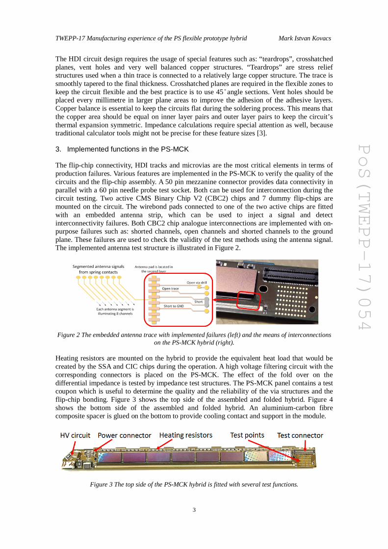
The flip-chip connectivity, HDI tracks and microvias are the most critical elements in terms ofproduction failures. Various features are implemented in the PS-MCK to verify the quality of thecircuits and the flip-chip assembly. A 50 pin mezzanine connector provides data connectivity inparallel with a 60 pin needle probe test socket. Both can be used for interconnection during thecircuit testing. Two active CMS Binary Chip V2 (CBC2) chips and 7 dummy flip-chips aremounted on the circuit. The wirebond pads connected to one of the two active chips are fittedwith an embedded antenna strip, which can be used to inject a signal and detectinterconnectivity failures. Both CBC2 chip analogue interconnections are implemented with on-purpose failures such as: shorted channels, open channels and shorted channels to the groundplane. These failures are used to check the validity of the test methods using the antenna signal.The implemented antenna test structure is illustrated in Figure 2.
Figure 2 The embedded antenna trace with implemented failures (left) and the means of interconnectionson the PS-MCK hybrid (right).
Heating resistors are mounted on the hybrid to provide the equivalent heat load that would becreated by the SSA and CIC chips during the operation. A high voltage filtering circuit with thecorresponding connectors is placed on the PS-MCK. The effect of the fold over on thedifferential impedance is tested by impedance test structures. The PS-MCK panel contains a testcoupon which is useful to determine the quality and the reliability of the via structures and theflip-chip bonding. Figure 3 shows the top side of the assembled and folded hybrid. Figure 4shows the bottom side of the assembled and folded hybrid. An aluminium-carbon fibrecomposite spacer is glued on the bottom to provide cooling contact and support in the module.
Figure 3 The top side of the PS-MCK hybrid is fitted with several test functions.

PoS(TWEPP-17)054
TWEPP-17 Manufacturing experience of the PS flexible prototype hybrid Mark Istvan Kovacs
4
Figure 4 The bottom side of the PS-MCK hybrid is hosting the rest of the test features.
4. Quality test results
The quality of the PS-MCK was tested by the manufacturer and CERN. X-ray, cross-sectionanalysis, scanning acoustic microscopy were applied on a sampling basis at the manufacturer’spremises. Visual inspection, weighing and functional testing were carried out on each deliveredcircuit at CERN [4].
4.1. Checks before the assembly
A quality check of components is essential before assembly. It is advised to check the quality ofbumps on flip-chips as defects are often affecting these delicate objects. It is also important tocheck the parameters of the components and verify that they conform to the specifications.Figure 5 shows examples of defects found during the checks before assembly.
Figure 5 Damaged flip-chips and spacer found by the inspection before assembly.
4.2. Results of production testing
All the three manufacturer consortia were able to deliver functional circuits. The antenna testmethod was able to detect 6 out of the 8 implemented opens. The short detection method wasable to detect all the shorted channels. Both methods showed good reproducibility and precision.The Panasonic 50 pin mezzanine connector and the needle probe tester were also successful toprovide interconnection during the functional testing. Details of the test results can be found in[4]. The hybrid assembly was successful because the hybrid geometry followed the designspecifications.
5. Problems and solutions
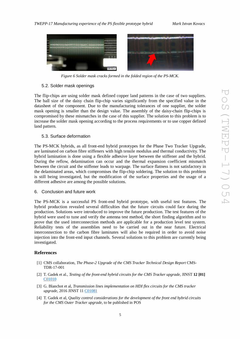
5.1. Solder mask fractures
The PS-MCK is folded sharply with a fold radius of 0.575 mm in order to fit in the PS moduledesign concept. This tight folding requires special flexible solder mask materials. One of thesuppliers used Peters Elpemer® SD 2463 FLEX-HF which has a minimum allowed bend radiusof 1.5 mm. As a result, cracks were formed in the solder mask and these cracks propagatedthrough the first copper layer. The traces in the first layer were cracked. The solution to thisproblem is to use a solder mask material that is more flexible, for example the Nippon PolytechCorp. NPR 80. The cracks are illustrated in Figure 6.
PoS(TWEPP-17)054
TWEPP-17 Manufacturing experience of the PS flexible prototype hybrid Mark Istvan Kovacs
5
Figure 6 Solder mask cracks formed in the folded region of the PS-MCK.
5.2. Solder mask openings
The flip-chips are using solder mask defined copper land patterns in the case of two suppliers.The ball size of the daisy chain flip-chip varies significantly from the specified value in thedatasheet of the component. Due to the manufacturing tolerances of one supplier, the soldermask opening is smaller than the design value. The assembly of the daisy-chain flip-chips iscompromised by these mismatches in the case of this supplier. The solution to this problem is toincrease the solder mask opening according to the process requirements or to use copper definedland pattern.
5.3. Surface deformation
The PS-MCK hybrids, as all front-end hybrid prototypes for the Phase Two Tracker Upgrade,are laminated on carbon fibre stiffeners with high tensile modulus and thermal conductivity. Thehybrid lamination is done using a flexible adhesive layer between the stiffener and the hybrid.During the reflow, delamination can occur and the thermal expansion coefficient mismatchbetween the circuit and the stiffener leads to warpage. The surface flatness is not satisfactory inthe delaminated areas, which compromises the flip-chip soldering. The solution to this problemis still being investigated, but the modification of the surface properties and the usage of adifferent adhesive are among the possible solutions.
6. Conclusion and future work
The PS-MCK is a successful PS front-end hybrid prototype, with useful test features. Thehybrid production revealed several difficulties that the future circuits could face during theproduction. Solutions were introduced to improve the future production. The test features of thehybrid were used to tune and verify the antenna test method, the short finding algorithm and toprove that the used interconnection methods are applicable for a production level test system.Reliability tests of the assemblies need to be carried out in the near future. Electricalinterconnection to the carbon fibre laminates will also be required in order to avoid noiseinjection into the front-end input channels. Several solutions to this problem are currently beinginvestigated.
References
[1] CMS collaboration, The Phase-2 Upgrade of the CMS Tracker Technical Design Report CMS-TDR-17-001
[2] T. Gadek et al., Testing of the front-end hybrid circuits for the CMS Tracker upgrade, JINST 12 [01]C01010
[3] G. Blanchot et al, Transmission lines implementation on HDI flex circuits for the CMS trackerupgrade, 2016 JINST 11 C01081
[4] T. Gadek et al, Quality control considerations for the development of the front end hybrid circuitsfor the CMS Outer Tracker upgrade, to be published in POS