manual técnico kf600d
TRANSCRIPT

Date: February, 2008 / Issue 1.0
Serv
ice M
an
ual
Mo
del : K
F600d
Service ManualKF600d

LGE Internal Use OnlyCopyright © 2007 LG Electronics. Inc. All right reserved. Only for training and service purposes
- 3 -
* The information in this manual is subject to change without notice and should not be construed as acommitment by LGE Inc. Furthermore, LGE Inc. reserves the right, without notice, to make changes toequipment design as advances in engineering and manufacturing methods warrant.
* This manual provides the information necessary to install, program, operate and maintain the KF600.
REVISED HISTORY
Editor Date Issue Contents of Changes S/W Version
D.H.AHN 12/24 0.1

- 4 -LGE Internal Use Only Copyright © 2007 LG Electronics. Inc. All right reserved. Only for training and service purposes

LGE Internal Use OnlyCopyright © 2007 LG Electronics. Inc. All right reserved. Only for training and service purposes
- 5 -
1. INTRODUCTION ...............................71.1 Purpose .................................................. 71.2 Regulatory Information............................ 71.3 ABBREVIATION ..................................... 9
2. PERFORMANCE.............................112.1 H/W Features.........................................112.2 Technical specification...........................12
3. TECHNICAL BRIEF ........................193.1 KF600 Functional Block diagram.... .......193.2 Baseband Processor (BBP)
Introduction ............................................203.3 Power management IC ..........................323.4 Power ON/OFF ......................................373.5 SIM & uSD interface ..............................383.6 Memory ..................................................403.7 LCD Display ...........................................413.8 Keypad Switching & Scanning ...............433.9 Keypad back-light illumination ...............443.10 LCD back-light illumination ..................453.11 Battery current consumption monitor ...463.12 JTAG & ETM interface connector ........463.13 ISP(Image Signal Processor)...............473.14 Audio....................................................483.15 Multi port switch ...................................513.16 charging circuit .....................................523.17 FM radio & BLUETOOTH ....................533.18 18pin Multi Media Interface connector .563.19 Touchpad Interface ..............................583.20 General Description .............................593.21 Receiver part........................................613.22 Transmitter part....................................623.23 RF synthesizer .....................................633.24 VCTCXO..............................................633.25 Front End Module control.....................643.26 Power Amplifier Module .......................653.27 Mode Selection ....................................663.28 PAM Schematic ...................................66
4. PCB layout......................................674.1 Main & Sub PCB component
placement ..............................................67
5. Trouble shooting............................715.1 Trouble shooting test setup....................715.2 Power on Trouble...................................725.3 Charging trouble ....................................755.4 LCD display trouble................................775.5 Camera Trouble .....................................795.6 Receiver & Speaker trouble ...................815.7 Microphone trouble ................................835.8 Vibrator trouble ......................................845.9 Keypad back light trouble.......................865.10 SIM & uSD trouble ...............................885.11 Touch pad trouble ................................915.12 Trouble Shooting of Receiver Part.......925.13 Trouble Shooting of Transmitter Part...98
6. Download & S/W upgrade...............1076.1 S/W download setup ............................1076.2 Download program user guide.............108
7. CIRCUIT DIAGRAM.......................111
8. BGM PIN MAP...............................117
9. PCB LAYOUT................................123
10. RF Calibration ............................12910.1 Test Equipment Setup .......................12910.2 Calibration Step .................................129
11. Stand-alone Test ........................13511.1 Test Program Setting .........................15711.3 Rx Test...............................................159
12. ENGINEERING MODE................139
13. EXPLODED VIEW &REPLACEMENT PART LIST ..... 141
13.1 Exploded View .................................. 141
13.2 Replacement Parts ............................14313.3 Accessory ......................................... 165
Table Of Contents

- 6 -LGE Internal Use Only Copyright © 2007 LG Electronics. Inc. All right reserved. Only for training and service purposes

- 7 -
1. INTRODUCTION
1.1. Purpose
This manual provides the information necessary to repair, calibration, description and download thefeatures of the KF600.
1.2. Regulatory Information
A. Security
Toll fraud, the unauthorized use of telecommunications system by an unauthorized part (for example,persons other than your company’s employees, agents, subcontractors, or person working on yourcompany’s behalf) can result in substantial additional charges you’re your telecommunicationsservices. System users are responsible for the security of own system.There are may be risks of toll fraud associated with your telecommunications system. System usersare responsible for programming and configuring the equipment to prevent unauthorized use. LGEdoes not warrant that this product is immune from the above case but will prevent unauthorized use ofcommon-carrier telecommunication service of facilities accessed through or connected to it. LGE willnot be responsible for any charges that result from such unauthorized use.
B. Incidence of Harm
If a telephone company determines that the equipment provided to customer is faulty and possiblycausing harm or interruption in service to the telephone network, it should disconnect telephoneservice until repair can be done. A telephone company may temporarily disconnect service as long asrepair is not done.
C. Changes in Service
A local telephone company may make changes in its communications facilities or procedure. If thesechanges could reasonably be expected to affect the use of the KF600 or compatibility with the network,the telephone company is required to give advanced written notice to the user, allowing the user to takeappropriate steps to maintain telephone service.
D. Maintenance Limitations
Maintenance limitations on the KF600 must be performed only at the LGE or its authorized agents.The user may not make any changes and/or repairs expect as specifically noted in this manual.Therefore, note that unauthorized alternations or repair may affect the regulatory status of the systemand may void any remaining warranty.
1. INTRODUCTION
LGE Internal Use OnlyCopyright © 2007 LG Electronics. Inc. All right reserved. Only for training and service purposes

- 8 -
1. INTRODUCTION
E. Notice of Radiated Emissions
The KF600 complies with rules regarding radiation and radio frequency emission as defined by localregulatory agencies. In accordance with these agencies, you may be required to provide informationsuch as the following to the end user.
F. Pictures
The pictures in this manual are for illustrative purposes only; your actual hardware may look slightlydifferent.
G. Interference and Attenuation
An KF600 may interfere with sensitive laboratory equipment, medical equipment, etc. Interferencefrom unsuppressed engines or electric motors may cause problems.
H. Electrostatic Sensitive Devices
ATTENTION
Boards, which contains Electrostatic Sensitive Device(ESD), are indicated by the sign.Following information is ESD handling: Service personnel should ground themselves by using a wriststrap when exchange system boards.When repairs are made to a system board, they should spread the floor with anti-static mat which isalso grounded. Use a suitable, grounded soldering iron. Keep sensitive parts in these protectivepackages until these are used. When returning system boards or parts such as EEPROM to thefactory, use the protective package as described.
LGE Internal Use Only Copyright © 2007 LG Electronics. Inc. All right reserved. Only for training and service purposes

- 9 -
1. INTRODUCTION
1.3. ABBREVIATION
For the purposes of this manual, following abbreviations apply:
LGE Internal Use OnlyCopyright © 2007 LG Electronics. Inc. All right reserved. Only for training and service purposes
APC Automatic Power Control
BB Baseband
BER Bit Error Ratio
CC-CV Constant Current - Constant Voltage
CLA Cigar Lighter Adapter
DAC Digital to Analog Converter
DCS Digital Communication System
dBm dB relative to 1 milli-watt
DSP Digital Signal Processing
EEPROM Electrical Erasable Programmable Read-Only Memory
EGPRS Enhanced General Packet Radio Service
EL Electroluminescence
ESD Electrostatic Discharge
FPCB Flexible Printed Circuit Board
GMSK Gaussian Minimum Shift Keying
GPIB General Purpose Interface Bus
GPRS General Packet Radio Service
GSM Global System for Mobile Communications
IPUI International Portable User Identity
IF Intermediate Frequency
LCD Liquid Crystal Display
LDO Low Drop Output
LED Light Emitting Diode

LGE Internal Use Only Copyright © 2007 LG Electronics. Inc. All right reserved. Only for training and service purposes
1. INTRODUCTION
- 10 -
LGE LG Electronics
OPLL Offset Phase Locked Loop
PAM Power Amplifier Module
PCB Printed Circuit Board
PGA Programmable Gain Amplifier
PLL Phase Locked Loop
PSTN Public Switched Telephone Network
RF Radio Frequency
RLR Receiving Loudness Rating
RMS Root Mean Square
RTC Real Time Clock
SAW Surface Acoustic Wave
SIM Subscriber Identity Module
SLR Sending Loudness Rating
SRAM Static Random Access Memory
STMR Side Tone Masking Rating
TA Travel Adapter
TDD Time Division Duplex
TDMA Time Division Multiple Access
UART Universal Asynchronous Receiver/Transmitter
VCO Voltage Controlled Oscillator
VCTCXO Voltage Control Temperature Compensated Crystal Oscillator
WAP Wireless Application Protocol
8PSK 8 Phase Shift Keying
- 11 -
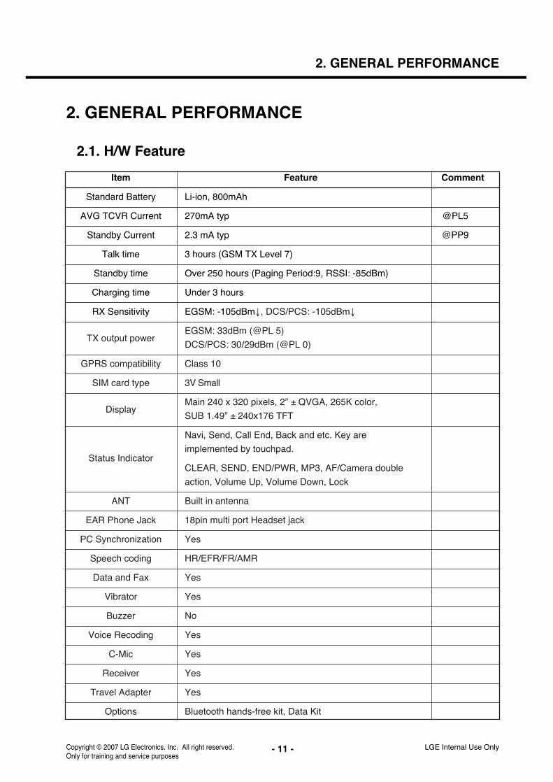
2. GENERAL PERFORMANCE
2.1. H/W Feature
2. GENERAL PERFORMANCE
LGE Internal Use OnlyCopyright © 2007 LG Electronics. Inc. All right reserved. Only for training and service purposes
Item Feature Comment
Standard Battery Li-ion, 800mAh
AVG TCVR Current 270mA typ @PL5
Standby Current 2.3 mA typ @PP9
Talk time 3 hours (GSM TX Level 7)
Standby time Over 250 hours (Paging Period:9, RSSI: -85dBm)
Charging time Under 3 hours
RX Sensitivity EGSM: -105dBm↓, DCS/PCS: -105dBm↓
TX output powerEGSM: 33dBm (@PL 5)
DCS/PCS: 30/29dBm (@PL 0)
GPRS compatibility Class 10
SIM card type 3V Small
DisplayMain 240 x 320 pixels, 2” ± QVGA, 265K color,
SUB 1.49” ± 240x176 TFT
Navi, Send, Call End, Back and etc. Key are
Status Indicatorimplemented by touchpad.
CLEAR, SEND, END/PWR, MP3, AF/Camera double
action, Volume Up, Volume Down, Lock
ANT Built in antenna
EAR Phone Jack 18pin multi port Headset jack
PC Synchronization Yes
Speech coding HR/EFR/FR/AMR
Data and Fax Yes
Vibrator Yes
Buzzer No
Voice Recoding Yes
C-Mic Yes
Receiver Yes
Travel Adapter Yes
Options Bluetooth hands-free kit, Data Kit

- 12 -
2. GENERAL PERFORMANCE
2.2. Technical specification
LGE Internal Use Only Copyright © 2007 LG Electronics. Inc. All right reserved. Only for training and service purposes
Item Description Specification
GSM900
TX: 890 + 0.2 x n MHz
RX: 935 + 0.2 x n MHz (n = 1 ~ 124)
EGSM
TX: 890 + 0.2 x (n-1024) MHz
1 Frequency BandRX: 935 + 0.2 x (n-1024) MHz (n = 975 ~ 1023)
DCS1800
TX: 1710 + ( n-511 ) x 0.2 MHz (n = 512 ~ 885)
RX: TX + 95 MHz
PCS1900
TX: 1850.2 + ( n-512 ) x 0.2 MHz (n = 512 ~ 810)
RX: TX + 80MHz
2 Phase ErrorRMS < 5 degrees
Peak < 20 degrees
3 Frequency Error < 0.1ppm
GSM900/EGSM
Level Power Toler. Level Power Toler.
5 33 dBm 2dB 13 17 dBm 3dB
6 31 dBm 3dB 14 15 dBm 3dB
7 29 dBm 3dB 15 13 dBm 3dB
8 27 dBm 3dB 16 11 dBm 5dB
9 25 dBm 3dB 17 9 dBm 5dB
10 23 dBm 3dB 18 7 dBm 5dB
11 21 dBm 3dB 19 5 dBm 5dB
12 19 dBm 3dB
4 Power Level DCS1800/PCS1900
Level Power Toler. Level Power Toler.
0 30 dBm 2dB 8 14 dBm 3dB
1 28 dBm 3dB 9 12 dBm 4dB
2 26 dBm 3dB 10 10 dBm 4dB
3 24 dBm 3dB 11 8 dBm 4dB
4 22 dBm 3dB 12 6 dBm 4dB
5 20 dBm 3dB 13 4 dBm 4dB
6 18 dBm 3dB 14 2 dBm 5dB
7 16 dBm 3dB 15 0 dBm 5dB

- 13 -
2. GENERAL PERFORMANCE
LGE Internal Use OnlyCopyright © 2007 LG Electronics. Inc. All right reserved. Only for training and service purposes
Item Description Specification
GSM900/EGSM
Offset from Carrier (kHz). Max. dBc
100 +0.5
200 -30
250 -33
400 -60
600 ~ <1,200 -60
1,200 ~ <1,800 -60
1,800 ~ <3,000 -63
3,000 ~ <6,000 -65
5Output RF Spectrum 6,000 -71
(due to modulation) DCS1800/PCS1900
Offset from Carrier (kHz). Max. dBc
100 +0.5
200 -30
250 -33
400 -60
600 ~ <1,200 -60
1,200 ~ <1,800 -60
1,800 ~ <3,000 -65
3,000 ~ <6,000 -65
6,000 -73
GSM900/EGSM
Offset from Carrier (kHz) Max. (dBm)
Output RF Spectrum 400 -196
(due to switching transient) 600 -21
1,200 -21
1,800 -24

- 14 -
2. GENERAL PERFORMANCE
LGE Internal Use Only Copyright © 2007 LG Electronics. Inc. All right reserved. Only for training and service purposes
Item Description Specification
DCS1800/PCS1900
Offset from Carrier (kHz). Max. (dBm)
Output RF Spectrum 400 -226
(due to switching transient) 600 -24
1,200 -24
1,800 -27
7 Spurious Emissions Conduction, Emission Status
EGSM
8 Bit Error RatioBER (Class II) < 2.439% @-102dBm
DCS1800/PCS1900BER (Class II) < 2.439% @-100dBm
9 Rx Level Report accuracy
10 SLR 8 3 dB
Frequency (Hz) Max.(dB) Min.(dB)
100 -12 -
200 0 -
300 0 -12
11 Sending Response 1,000 0 -6
2,000 4 -6
3,000 4 -6
3,400 4 -9
4,000 0 -
12 RLR 2 3 dB
Frequency (Hz) Max.(dB) Min.(dB)
100 -12 -
200 0 -
300 2 -7
500 * -5
13 Receiving Response 1,000 0 -5
3,000 2 -5
3,400 2 -10
4,000 2
* Mean that Adopt a straight line in between 300 Hzand 1,000 Hz to be Max. level in the range.

- 15 -
2. GENERAL PERFORMANCE
LGE Internal Use OnlyCopyright © 2007 LG Electronics. Inc. All right reserved. Only for training and service purposes
Item Description Specification
14 STMR 13 5 dB
15 Stability Margin > 6 dB
dB to ARL (dB) Level Ratio (dB)
-35 17.5
-30 22.5
-20 30.716 Distortion
-10 33.3
0 33.7
7 31.7
10 25.5
17 Side Tone Distortion Three stage distortion < 10%
18System frequency
2.5ppm(26 MHz) tolerance
19 32.768KHz tolerance 30ppm
Standby20 Power consumption
- Normal 3 mA(@PP9)
21 Talk TimeEGSM/Lvl 7 (Battery Capacity 800mA):180 minEGSM/Lvl12(Battery Capacity 800 mA):320minUnder conditions, at least 300 hours:1. Brand new and full 800mAh battery
22 Standby Time2. Full charge, no receive/send and keep GSM in idle mode.3. Broadcast set off.4. Signal strength display set at 3 level above.5. Backlight of phone set off.At least 65 dB under below conditions:
23 Ringer Volume 1. Ringer set as ringer.2. Test distance set as 50 cm
24 Charge CurrentFast Charge: < 550 mASlow Charge: < 120 mA
Antenna Bar Number Power
7 >-92 dBm ~
5 -97dBm ~ -93dBm
25 Antenna Display4 -100dBm ~ -98dBm
2 -103dBm ~ -101dBm
1 -105dBm ~ -104dBm
0 < -106 dBm
Off No Service

LGE Internal Use Only Copyright © 2007 LG Electronics. Inc. All right reserved. Only for training and service purposes
2. GENERAL PERFORMANCE
- 16 -
Item Description Specification
Battery Bar Number Voltage( 0.05V)
3 3.69V ~ 4.2V
26 Battery Indicator 2 3.53V ~ 3.69V
1 3.43V ~ 3.53V
0 3.30V ~ 3.43V
27 Low Voltage Warning3.53V↓ 0.05V (Call)
3.43V↓ 0.05V (Standby)
28 Forced shut down Voltage 3.3 0.05 V
Li-ion Battery
29 Battery TypeStandard Voltage = 3.7 VBattery full charge voltage = 4.2 VCapacity: 800mAh
Switching-mode charger31 Travel Charger Input: 100 ~ 240 V, 50/60Hz
Out put: 4.8, 0.9A

LGE Internal Use OnlyCopyright © 2007 LG Electronics. Inc. All right reserved. Only for training and service purposes
2. GENERAL PERFORMANCE
- 17 -
* EDGE RF Specification (Option: is not serviced for “EDGE mode”)
Item Description Specification
1 RMS EVM 9%2 Peak EVM 30%3 95th Percentile EVM 15%4 Origin Offset Suppression ≥ 30dB
GSM900/EGSM
Level Power Toler. Level Power Toler.
5 27dBm 3dB 13 17dBm 3dB
6 27dBm 3dB 14 15dBm 3dB
7 27dBm 3dB 15 13dBm 3dB
8 27dBm 3dB 16 11dBm 5dB
9 25dBm 3dB 17 9dBm 5dB
10 23dBm 3dB 18 7dBm 5dB
11 21dBm 3dB 19 5dBm 5dB
5 Power Level 12 19dBm 3dB
DCS1800, PCS1900
Level Power Toler. Level Power Toler.
0 26/25dBm 3dB 8 14 dBm 3dB
1 26/25dBm 3dB 9 12 dBm 4dB
2 26/25dBm 3dB 10 10 dBm 4dB
3 24 dBm 3dB 11 8 dBm 4dB
4 22 dBm 3dB 12 6 dBm 4dB
5 20 dBm 3dB 13 4 dBm 4dB
6 18 dBm 3dB 14 2 dBm 5dB
7 16 dBm 3dB 15 0 dBm 5dB
6 Output RF Spectrum GSM900/EGSM
(due to modulation) Offset from carrier(kHz) Max. dBc
100 +0.5
200 -30
250 -33
400 -54
600 ~ <1,200 -60
1,200 ~ <1,800 -60
1,800 ~ <3,000 -63
3,000 ~ <6,000 -65
6,000 -71

LGE Internal Use Only Copyright © 2007 LG Electronics. Inc. All right reserved. Only for training and service purposes
2. GENERAL PERFORMANCE
- 18 -
Item Description Specification
6 Output RF Spectrum DCS1800, PCS1900
(due to modulation) Offset from carrier(kHz) Max. dBc
100 +0.5
200 -30
250 -33
400 -54
600 ~ <1,200 -60
1,200 ~ <1,800 -60
1,800 ~ <3,000 -63
3,000 ~ <6,000 -65
6,000 -71
7 Output RF Spectrum GSM900/EGSM
(due to switching transient) Offset from carrier(kHz) Max. dBm
400 -23
600 -26
1,200 -27
1,800 --30
DCS1800, PCS1900
Offset from carrier(kHz) Max. dBm
400 -23
600 -26
1,200 -27
1,800 -30

LGE Internal Use OnlyCopyright © 2007 LG Electronics. Inc. All right reserved. Only for training and service purposes
3. TECHNICAL BRIEF
- 19 -
Baseband circuit
3.1. KF600 Functional Block diagram.
The functional component arrangement is mentioned below diagram.
3. TECHNICAL BRIEF
Figure 2 KF600 Functional block diagram
SIMMICRO SD
BT+FMBC5
PAMSKY77340
FEMLMSP43QA
RF TRPMB6272
PMICPMB6821
BBPPMB8877
ISPMV9319
2î TFT LCD
1.5î TFT LCD
2î TFT LCD
1.5î TFT LCD
#0*
987
654
321
ENDCSend
#0*
987
654
321
ENDCSend
SPK
VIBVIB
CP
26M26MHzFMFM
CP
PMICPMIC
VBATVBATPMICPMICExt. LDOExt. LDO
VBATVBAT
VBATVBAT
Ext. LDOExt. LDO

- 20 -
3. TECHNICAL BRIEF
3.2. Baseband Processor (BBP) Introduction
3.2.1. General Description
S-GOLD3™ is a GSM/EDGE single chip mixed signal Baseband IC containing all analog and digitalfunctionality of a cellular radio. Additionally S-GOLD3™ Provides multimedia extensions such ascamera, software MIDI, MP3 sound. It is designed as a single chip solution, integrating the digital andmixed signal portions of the base band in 0.09um, 1.2V technology.
The chip will fully support the FR, EFR, HR and AMR-NB vocoding.
S-GOLD3™ support multi-slot operation modes HSCSD (up to class 10), GPRS for high speed dataapplication (up to class 12) and EGPRS (up to class 12) without additional external hardware.
LGE Internal Use Only Copyright © 2007 LG Electronics. Inc. All right reserved. Only for training and service purposes
Figure 3 Top level block diagram of the S-GOLD3™ (PMB8877)

- 21 -
3. TECHNICAL BRIEF
3.2.2. Block Description
• Processing coreARM926EJ-S 32 bit processor core for controller functions. The ARM926EJ-S includes an MMU,and the Jazelle Java extension for Java acceleration.- TEAKLite DSP core
• ARM-Memory- 32k Byte Boot ROM on the AHB- 96k Byte SRAM on the AHB, flexibly usable as program or data RAM- 16k Byte Cache for Program (internal)- 8k Byte tightly coupled memory for Program(internal)- 8k Byte Cache for Data(internal)- 8k Byte tightly coupled memory for Data(internal)
• DSP-Memory- 104K x 16bit Program ROM- 8k x 16bit Program RAM- 60k x 16bit Data ROM- 37k x 16bit Data RAM- Incremental Redundancy(IR) Memory of 35904 words of 16bit
• Shared Memory Block1.5K x 32bit Shared RAM(dual ported) between controller system and TEAKLite.
• Controller Bus systemThe processor cores and their peripherals are connected by powerful buses. Multi-layer AHB forconnecting the ARM and the other master capable building blocks with the internal and externalmemories and with the peripheral buses.
• Clock systemThe clock system allows widely independent selection of frequencies for the essential parts of theS-GOLD3. Thus power consumption and performance can be optimized for each application.
• Functional Hardware block- CPU and DSP Timers- MOVE coprocessor performing motion estimation for video encoding algorithms (H.263, MPEG-4)- Programmable PLL with additional phase shifters for system clock generation- GSM Timer Module that off-loads the CPU from radio channel timing- GMSK / 8-PSK Modulator according to GSM-standard 05.04 (5/2000)- GMSK Modulator: gauss-filter with B*T=0.3- EDGE Modulator: 8PSK-modulation with linearized GMSK-Pulse-Filter- Hardware accelerators for equalizer and channel decoding.- Incremental Redundancy memory for EDGE class 12 support- A5/1, A5/2, A5/3 Cipher unit- GEA1, GEA2, GEA3 Cipher Unit to support GPRS data transmission
LGE Internal Use OnlyCopyright © 2007 LG Electronics. Inc. All right reserved. Only for training and service purposes

- 22 -
3. TECHNICAL BRIEF
- Advanced static and dynamic power management features including TDMA-Frame synchronouslow power mode and enhanced CPU modes(idle and sleep modes)
- Pulse Number Modulation output for Automatic Frequency Correction(AFC)- Serial RF Control interface: support of direct conversion RF- A Universal Serial Interface(USIF) enabling asynchronous (UART) of synchronous (SPI) serial
data transmission- 3 USIF with autobaud detection, hardware flow control and integrated- A dedicated Fas IfDA Controller supporting IrDA’s SIR,MIR and FIR standards (up to 4Mbps)- I2C-bus interface (e.g. connection to S/M power)- A fast display interface supporting serial and parallel interconnection- An ITU-R BT.656 compatible Camera interface.- Programmable clock output for a camera- An multimedia/Secure Digital Card Interface (MMCI/SD: SDIO capable)
3.2.3. External Devices connected to memory interface
Table 1. Memory interface
3.2.4. RF Interface (T_OUT)
S-Gold3 uses this interface to control RF IC and Peripherals. 13 signals are provided switch on/off RFICs Periodically each TDMA frame.
Table 2. RF Interface Spec.
LGE Internal Use Only Copyright © 2007 LG Electronics. Inc. All right reserved. Only for training and service purposes
Device Name Maker Remark
FLASH K5E1G12ACA-D075 Samsung Synchronous / A synchronous
DDR K5E1G12ACA-D075 Samsung Synchronous 133MHz
LCD IM200DST2A LGIT 8bit access 2 times transmission
Melody IC Not Used S/W Infineon Software CODEC
T_OUT
Resource Interconnection Description
T_OUT0 TXON_PA PAM Power on
T_OUT1 Other function -
T_OUT2 PA_BAND TX RF band select
T_OUT3 ANT_SW1 FEM control
T_OUT4 ANT_SW2 FEM control
T_OUT5 ANT_SW3 FEM control
T_OUT6 MODE PAM Mode select

- 23 -
3. TECHNICAL BRIEF
3.2.5. USART Interface
KF600 have three USIF Drivers as follow :- USIF1: Hardware Flow Control / SW upgrade / Calibration- USIF2: Not used Rx, Tx and CTS, RTS use BT Interface- USIF3: BT Interface
Table 3. USIF Interface Spec.
3.2.6. ADC channel
BBP ADC block is composed of 7 external ADC channel. This block operates charging process andother related process by reading battery voltage and other analog values.
Table 4. S-Gold3 ADC channel usage
LGE Internal Use OnlyCopyright © 2007 LG Electronics. Inc. All right reserved. Only for training and service purposes
USIF1
Resource Name Remark
USART0_TXD TXD Transmit Data
USART0_RXD RXD Receive Data
USART0_CTS USB_DP
USART0_RTS USB_DM
USIF2
USART1_TXD NC NC
USART1_RXD NC NC
USART1_CTS BT_CTS
USART1_RTS BT_RTS.
USIF3
USIF3_TXD BT_TX BT Transmit tx
USIF3_RXD BT_RX BT Receive rx
ADC channel
Resource Interconnection Description
M0 BAT_ID Battery temperature measure
M1 RF_TEMP RF block temperature measure
M2 REMOTE_ADC Remote Control
M3 JACK_TYPE Accessory type detect
M4 N.C
M5 N.C
M6 N.C
M7 H/W VERSION S-Gold2 H/W version detect
M8 VSUPPLY Battery supply voltage measure
M9 I_MONITOR Current consumption measure
M10 N.C
- 24 -
3. TECHNICAL BRIEF
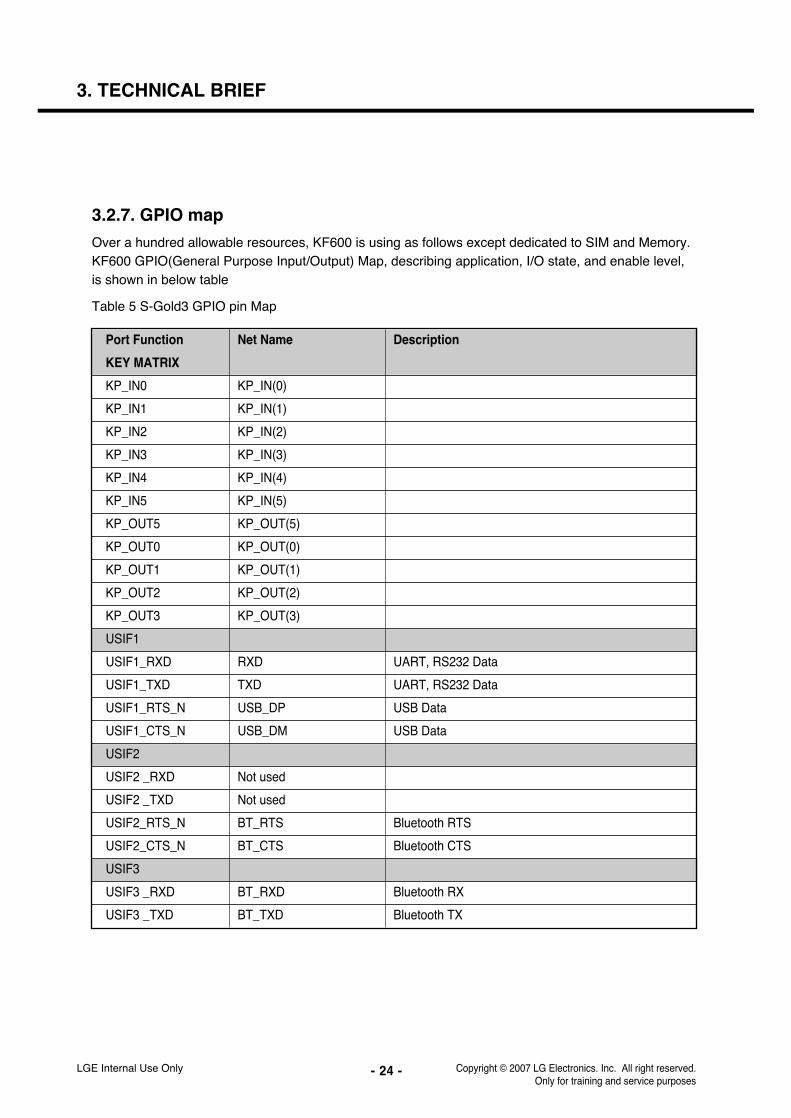
3.2.7. GPIO map
Over a hundred allowable resources, KF600 is using as follows except dedicated to SIM and Memory.KF600 GPIO(General Purpose Input/Output) Map, describing application, I/O state, and enable level,is shown in below table
Table 5 S-Gold3 GPIO pin Map
LGE Internal Use Only Copyright © 2007 LG Electronics. Inc. All right reserved. Only for training and service purposes
Port Function Net Name Description
KEY MATRIX
KP_IN0 KP_IN(0)
KP_IN1 KP_IN(1)
KP_IN2 KP_IN(2)
KP_IN3 KP_IN(3)
KP_IN4 KP_IN(4)
KP_IN5 KP_IN(5)
KP_OUT5 KP_OUT(5)
KP_OUT0 KP_OUT(0)
KP_OUT1 KP_OUT(1)
KP_OUT2 KP_OUT(2)
KP_OUT3 KP_OUT(3)
USIF1
USIF1_RXD RXD UART, RS232 Data
USIF1_TXD TXD UART, RS232 Data
USIF1_RTS_N USB_DP USB Data
USIF1_CTS_N USB_DM USB Data
USIF2
USIF2 _RXD Not used
USIF2 _TXD Not used
USIF2_RTS_N BT_RTS Bluetooth RTS
USIF2_CTS_N BT_CTS Bluetooth CTS
USIF3
USIF3 _RXD BT_RXD Bluetooth RX
USIF3 _TXD BT_TXD Bluetooth TX
- 25 -
3. TECHNICAL BRIEF
LGE Internal Use OnlyCopyright © 2007 LG Electronics. Inc. All right reserved. Only for training and service purposes
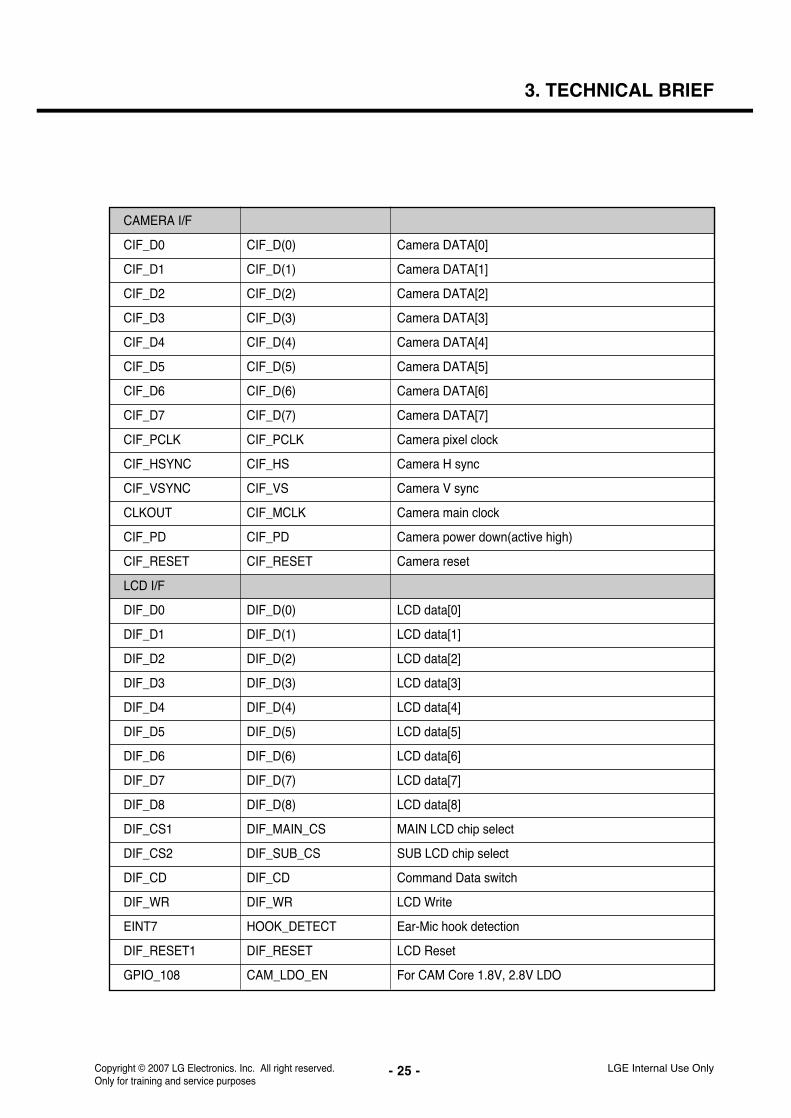
CAMERA I/F
CIF_D0 CIF_D(0) Camera DATA[0]
CIF_D1 CIF_D(1) Camera DATA[1]
CIF_D2 CIF_D(2) Camera DATA[2]
CIF_D3 CIF_D(3) Camera DATA[3]
CIF_D4 CIF_D(4) Camera DATA[4]
CIF_D5 CIF_D(5) Camera DATA[5]
CIF_D6 CIF_D(6) Camera DATA[6]
CIF_D7 CIF_D(7) Camera DATA[7]
CIF_PCLK CIF_PCLK Camera pixel clock
CIF_HSYNC CIF_HS Camera H sync
CIF_VSYNC CIF_VS Camera V sync
CLKOUT CIF_MCLK Camera main clock
CIF_PD CIF_PD Camera power down(active high)
CIF_RESET CIF_RESET Camera reset
LCD I/F
DIF_D0 DIF_D(0) LCD data[0]
DIF_D1 DIF_D(1) LCD data[1]
DIF_D2 DIF_D(2) LCD data[2]
DIF_D3 DIF_D(3) LCD data[3]
DIF_D4 DIF_D(4) LCD data[4]
DIF_D5 DIF_D(5) LCD data[5]
DIF_D6 DIF_D(6) LCD data[6]
DIF_D7 DIF_D(7) LCD data[7]
DIF_D8 DIF_D(8) LCD data[8]
DIF_CS1 DIF_MAIN_CS MAIN LCD chip select
DIF_CS2 DIF_SUB_CS SUB LCD chip select
DIF_CD DIF_CD Command Data switch
DIF_WR DIF_WR LCD Write
EINT7 HOOK_DETECT Ear-Mic hook detection
DIF_RESET1 DIF_RESET LCD Reset
GPIO_108 CAM_LDO_EN For CAM Core 1.8V, 2.8V LDO
- 26 -
3. TECHNICAL BRIEF
LGE Internal Use Only Copyright © 2007 LG Electronics. Inc. All right reserved. Only for training and service purposes
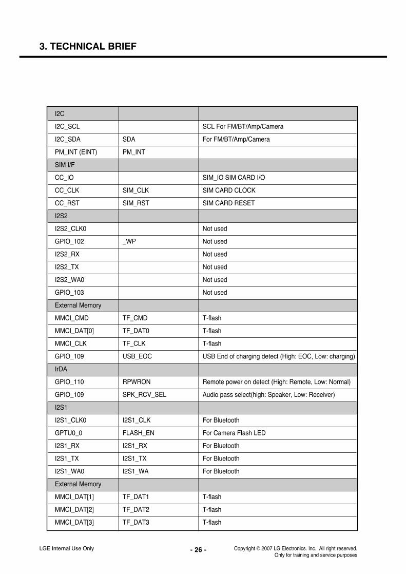
I2C
I2C_SCL SCL For FM/BT/Amp/Camera
I2C_SDA SDA For FM/BT/Amp/Camera
PM_INT (EINT) PM_INT
SIM I/F
CC_IO SIM_IO SIM CARD I/O
CC_CLK SIM_CLK SIM CARD CLOCK
CC_RST SIM_RST SIM CARD RESET
I2S2
I2S2_CLK0 Not used
GPIO_102 _WP Not used
I2S2_RX Not used
I2S2_TX Not used
I2S2_WA0 Not used
GPIO_103 Not used
External Memory
MMCI_CMD TF_CMD T-flash
MMCI_DAT[0] TF_DAT0 T-flash
MMCI_CLK TF_CLK T-flash
GPIO_109 USB_EOC USB End of charging detect (High: EOC, Low: charging)
IrDA
GPIO_110 RPWRON Remote power on detect (High: Remote, Low: Normal)
GPIO_109 SPK_RCV_SEL Audio pass select(high: Speaker, Low: Receiver)
I2S1
I2S1_CLK0 I2S1_CLK For Bluetooth
GPTU0_0 FLASH_EN For Camera Flash LED
I2S1_RX I2S1_RX For Bluetooth
I2S1_TX I2S1_TX For Bluetooth
I2S1_WA0 I2S1_WA For Bluetooth
External Memory
MMCI_DAT[1] TF_DAT1 T-flash
MMCI_DAT[2] TF_DAT2 T-flash
MMCI_DAT[3] TF_DAT3 T-flash

- 27 -
3. TECHNICAL BRIEF
LGE Internal Use OnlyCopyright © 2007 LG Electronics. Inc. All right reserved. Only for training and service purposes
Audio I/F
EPN1 RCV_N For Receiver
EPP1 RCV_P For Receiver
EPPA1 BBP_SND_L For Speaker
EPREF Reference
EPPA2 BBP_SND_R For Speaker
MICN1 MIC1_N For Mic
MICP1 MIC1_P For Mic
MICN2 MIC2_N For Headset Mic
MICP2 MIC2_P For Headset Mic
VMICP VMICP Power for MIC
VMICN VMICN Power for MIC
ADC
M0 BAT_ID Battery temperature measure
M1 RF_TEMP RF block temperature measure
M2 REMOTE_ADC Remote Control
M3 JACK_TYPE Accessory type detect
M7 H/W VERSION S-Gold2 H/W version detect
M8 VSUPPLY Battery supply voltage measure
M9 I_MONITOR Current consumption measure
M10 N.C
Reference
VREF
IREF
JTAG I/F
TDO TDO JTAG
TDI TDI JTAG
TMS TMS JTAG
TCK TCK JTAG
TRST_n _TRST JTAG
RTCK RTCK JTAG

- 28 -
3. TECHNICAL BRIEF
LGE Internal Use Only Copyright © 2007 LG Electronics. Inc. All right reserved. Only for training and service purposes
ETM I/F
TRIG_IN TRIG_IN ETM (Embedded Trace Macro Cell)
MON1 MON1 ETM
MON2 MON2 ETM
TRACESYNC TRACESYNC ETM
TRACECLK TRACECLK ETM
PIPESTAT[2] PIPESTAT2 ETM
PIPESTAT[1] PIPESTAT1 ETM
PIPESTAT[0] PIPESTAT0 ETM
TRACEPKT[0] TRACEPKT(0) ETM
TRACEPKT[1] TRACEPKT(1) ETM
TRACEPKT[2] TRACEPKT(2) ETM
TRACEPKT[3] TRACEPKT(3) ETM
TRACEPKT[4] TRACEPKT(4) ETM
TRACEPKT[5] TRACEPKT(5) ETM
TRACEPKT[6] TRACEPKT(6) ETM
TRACEPKT[7] TRACEPKT(7) ETM
Memory
MEM_AD[0] D(0)
MEM _AD[1] D(1)
MEM _AD[2] D(2)
MEM _AD[3] D(3)
MEM _AD[4] D(4)
MEM _AD[5] D(5)
MEM _AD[6] D(6)
MEM _AD[7] D(7)
MEM _AD[8] D(8)
MEM _AD[9] D(9)
MEM _AD[10] D(10)
MEM _AD[11] D(11)
MEM _AD[12] D(12)
MEM _AD[13] D(13)
MEM _AD[14] D(14)
MEM _AD[15] D(15)
MEM _WR_n _WR

- 29 -
3. TECHNICAL BRIEF
LGE Internal Use OnlyCopyright © 2007 LG Electronics. Inc. All right reserved. Only for training and service purposes
MEM _RD_n _RD
MEM _BC0_n _BC0
MEM _BC1_n _BC1
MEM _A[0] A(0)
MEM _A[1] A(1)
MEM _A[2] A(2)
MEM _A[3] A(3)
MEM _A[4] A(4)
MEM _A[5] A(5)
MEM _A[6] A(6)
MEM _A[7] A(7)
MEM _A[8] A(8)
MEM _A[9] A(9)
MEM _A[10] A(10)
MEM _A[11] A(11)
MEM _A[12] A(12)
MEM _A[13] A(13)
MEM _A[14] A(14)
MEM _A[15] A(15)
MEM _A[16] A(16)
MEM _A[17] A(17)
MEM _A[18] A(18)
MEM _A[19] A(19)
MEM _A[20] A(20)
MEM _A[21] A(21)
MEM _A[22] A(22)
MEM _A[23] A(23)
MEM _A[24] A(24)
MEM _CS0_n _FLASH1_CS INTEL NOR (64MB)
MEM _CS1_n _RAM_CS INTEL SDRAM (64MB)
MEM _CS2_n _FLASH2_CS Not used
MEM _CS3_n _CS3 Not used
MEM _ADV_n _ADV
MEM _RAS_n _RAS
MEM _CAS_n _CAS

- 30 -
3. TECHNICAL BRIEF
LGE Internal Use Only Copyright © 2007 LG Electronics. Inc. All right reserved. Only for training and service purposes
MEM _WAIT_n _WAIT
MEM _SDCLKO SDCLKO For Burst mode
MEM _SDCLKI SDCLKI For Burst mode
MEM _BFCLKO BFCLKO For Burst mode
MEM _BFCLKI BFCLKI For Burst mode
MEM _CKE CKE
Memory
FCDP_RBn FCDP
TDMA I/F
T_OUT0 TXON_PA PAM
GPIO_44 VIB_EN
T_OUT2 PA_BAND PAM
T_OUT3 ANT_SW1
T_OUT4 ANT_SW2
T_OUT5 ANT_SW3
T_OUT6 MODE PAM
KP_OUT4 KP_OUT(4)
EINT7 JACK_DETECT
CC1CC3IO LCD_BACKLIGHT LCD Backlight control
GPIO_53 LCD_ID LCD ID check
GPIO_54 _FM_RESET
RF I/F
RF_STR0 RF_EN
CC1CC5IO SLIDE_DETECT Slide on/off detection
RF_DATA RF_DA
RF_CLK RF_CLK
System Port
AFC AFC
CLKOUT0 Not used
[<=26MHz]

- 31 -
3. TECHNICAL BRIEF
LGE Internal Use OnlyCopyright © 2007 LG Electronics. Inc. All right reserved. Only for training and service purposes
F26M 26MHZ_MCLK 26M Main Clock
F32K to 32k crystal
OSC32K to 32k crystal
RESET_n _RESET
TRIG_OUT TRIG_OUT
RTC_OUT RTC_OUT
VCXO_EN VCXO_EN
DSP
GPIO_61 _BT_RESET
GPIO_62 SLED_BACKLIGHT Navi key LED Backlight Control
GPIO_63 _SIM_EN

- 32 -
3. TECHNICAL BRIEF
3.3. Power management IC
3.3.1. General Description
SM-POWER is a highly integrated Power and Battery Management IC for mobile handsets. It hasbeen specially designed for usage with S-Gold3. Although optimized for usage with the Infineon S-GOLD baseband device it is suitable for the S-GOLDlite and the E-GOLD+ baseband devices aswell. It also supports the cellular RF devices like SMARTi-DC, SMARTi-DC+, SMARTi-SD and theBluemoon Single, Infineon’s single chip solution for Bluetooth. If used with S-GOLD3 it provides allpower supply functions (except for the RF PA) for a complete advanced GSM Edge smart phoneminimizing external device count.
Block Description
• Highly efficient step-down converter for main digital baseband supply including Core, DSP andmemory interface (External Bus Unit).
• Support of S-GOLD standby power-down concept
• Low-drop-out (LDO) regulators for Flash and mobile RAM memory devices
• Voltage independent switching of two SIM cards
• LDO regulators for baseband I/O supply
• LDO regulator for analog mixed-signal section of S-GOLD
• Low-noise LDO regulators for RF devices
• Supply for Bluemoon Single, Infineon’s single chip solution for Bluetooth
• Audio amplifier 8 Ohms for handsfree operation and ringing
• Charge Control for charging Li-Ion/Polymer batteries under software control
• Pre-charge current generator with selectable current level
• RTC regulator with ultra-low quiescent current
• USB interface support for peripheral and mini-host mode
• Backlight LEDs driver with current selection and PWM dimming function
• Two single LED driver outputs for signaling
• Vibrator driver with adjustable voltage
• Fully controlable by software via I2C - Bus
• Temperature and battery voltage sensors
• Interrupt channels for peripherals
• System debug mode
• VQFN 48 package with heat sink and non-protruding leads
• Compatible with the Infineon E-GOLD+ V2 and V3
LGE Internal Use Only Copyright © 2007 LG Electronics. Inc. All right reserved. Only for training and service purposes

- 33 -
3. TECHNICAL BRIEF
SM-POWER is a further step on the successful E-Power product line with enhanced and optimizedfunctionality. SM-POWER features a baseband supply concept with a DC/DC step-down convertercascaded by two linear regulators- SM-POWER’s DC/DC converter makes up to 40 % reduction of battery current for smart phone
functions (e.g. organizer functions, games, MP3 decoding) possible.- SDBB has high efficiency up to 95% and also a power save mode.- Memory Interface is directly supported by the SDBB- SDBB can also act as main supply voltage for E-GOLD+ or S-GOLDlite baseband devices.- For S-GOLD two linear regulators for DSP and Core are cascaded after the SDBB.
SM-POWER supports the standby power-down concept of S-GOLD by temporarily switching off thelinear regulator for the DSP during mobile standby whenever this subsystem is not used. In this phasethe ARM controller and most peripherals including parts of the on-chip SRAM are kept powered-upwith power being supplied by the other linear regulator.SM-POWER includes a fully differential audio amplifier able to drive loads down to a nominal value of8 Ohm for usage in hands-free phones and for ringing
- 450 mW maximum output power- adjustable gain- mute switch SM-POWER also integrates a charging function for Li-Ion, Li-Polymer batteries- click and pop -protection SM-POWER also integrates a charging function for Li-Ion, Li-Polymer
batteries- Precharge current source with two current levels- Constant current / constant voltage charging with 3 different termination voltages- Programable charge current limitation for use with different batteries- Freely programable pulse charging to reduce the thermal power dissipation in the constant voltage
charging phase- Top-off charge current sensing SM-POWER completes the USB interface of S-GOLD- Regulated voltage for S-GOLD USB interface including reverse current and overvoltage protection- Switch to supply USB pull-up resistor- Mini-host pull down resistor functionality- Charge pump with internal switching capacitor for USB host VBUS supply voltage SM-POWER
fully supports LED and Vibra Motor functionality- no external components needed- driver for backlight LEDs adjustable in steps up to 140mA and with soft turn on and off by PWM
dimming- two driver outputs for single LEDs for precharge indication and signaling with i.e. change of colour-driver for Vibra Motor with adjustable voltages, soft startup / shutdown and current limitation
LGE Internal Use OnlyCopyright © 2007 LG Electronics. Inc. All right reserved. Only for training and service purposes

- 34 -
3. TECHNICAL BRIEF
SM-POWER offers several control functions- Power-on Reset Generator with logic state machine- I2C bus interface- I2C bus configurable mode control logic with ON (push-button or RTC), VCXOEN and LRF3EN
(wake-up by Bluetooth) inputs- Programable interrupt channels to handle peripherals like SIM, MMC and USB- Monitoring of charging functions- Undervoltage Shut-Down- Errorflags (volatile or non-volatile) from many power-supply functions and thermal sensor in order
to debug system- Overtemperature Shut-Down- Overtemperature Warning- Support of S-GOLD standby power-down concept- Support of S-GOLD Power-Down Pad Tristate Function
Table 6. LDO Output Table of SM-Power
LGE Internal Use Only Copyright © 2007 LG Electronics. Inc. All right reserved. Only for training and service purposes
LDO Net name Output Voltage Output Current Usage
SD1 1V35_Core 1.35V 600mA Core & for LDO
SD2 1V8_SD 1.8V 300mA Memory
VAUX 2V9_VAF 2.9V 100mA Cam Auto Focus
VIO 2V62_VIO 2.62V 100mA Peripherals
VSIM 2V9_SIM 2.9V 70mA SIM card
VMME 2V8_VMME 2.9V 150mA u-SD
VUMTS 2V85_AMP 2.85V 110mA Headset AMP
VUSB VUSB 3.1V 40mA Not used
VLED VLED 2.9V 10mA Not used
VAUDIOa 2V5_VAUDA 2.5V 200mA Stereo headset, Mono earpiece
VAUDIOb 2V5_VAUDB 2.5V 50mA Analog parts of S-Gold
VRF1 2V85_VRF 2.85V 150mA 2.85 V supply for SMARTi-PM
RF transceiver
VRF2 1V5_VRF 1,53V 100mA 1.5 V supply for SMARTi-PM
RF transceiver
VRF3 2V65_VBT 2.7V 150mA Bluetooth
VPLL 1V35_VPLL 1.35V 30mA S-GOLD3 PLL
VRTC 2V11_RTC 2.11V 4mA Real Time Clock
VAFC VAFC 2.65V 5mA Not used
VVIB 2V8_VLCD 2.8V 140mA LCD

- 35 -
3. TECHNICAL BRIEF
LGE Internal Use OnlyCopyright © 2007 LG Electronics. Inc. All right reserved. Only for training and service purposes
Figure 5. SM-Power Circuit Diagram of KF600
Figure 6 SM-Power circuit diagram with charging part
2V62_VIO
0.1uC236
VBAT
C23
210
u
TP202
NAR202
0.1u
C21
2C2400.1u
4.7K
R20
7
C2472.2u
C2282.2u
C21
31u
C2301u
10uHL201
22u
1V35_CORE
C237
0R213
C21
12.
2u
R20
40
EX
T_O
N
2V5_VAUDB
2V9_SIM2V11_RTC
R21
14.
7K
C21
5
VBAT
0.1u
R20
9N
A
2.2uC241
1uC245
2V5_VAUDA
R21
210
0K
100u
PMRSTn
VBAT
C206
C2392.2u 2.2u
C2482.2u1uC249C243
FB
201
2V85_AMP
2.2uC246C242
2.2u
4.7K
R20
8
VBAT
C21
02.
2u
1V8_SD
R21
04.
7K
U_VMIN
10u
C23
1
KD
S16
0E
2V85_VRF
D20
2
0.1uC201
C20
52.
2u
4.7K
C251
R20
6
2V8_VMME
2.2u
VBAT
VCHG_VUSB
2.2u
C203
C23510u
VBAT D20
1
KD
S16
0E
2.2uC202
SP
_IN
T
U_RCV
C2441u
VBAT
2.2uC250
2V8_VLCD1V8_SD
2.2u
C20
4
VVIBF11
WD
OG
L3
10uC234 H
6V
SS
28V
SS
29H
7
D5
VS
S3
J6V
SS
30
VS
S4
D6
D7
VS
S5
VS
S6
D8
E4
VS
S7
VS
S8
E5
E6
VS
S9
C7
VS
S_M
ON
O
VS
S_S
D1
H8
H4
VS
S_S
D2
D9
VS
S_V
RE
F
J11VUMTS
A4
VU
SB
F3
VS
S13
VS
S14
F4
F5
VS
S15
VS
S16
F6
F7
VS
S17
VS
S18
F8
F9
VS
S19
VS
S2
D4
VS
S20
G3
G4
VS
S21
VS
S22
G5
VS
S23
G6
G7
VS
S24
VS
S25
G8
G9
VS
S26
VS
S27
H5
C11VMME
C2VPIN
VP
LLA
10
VR
EF
C8
VR
EF
EX
_MA
5
F10VRF1
VRF2D11
E10VRF3
VRTCH10
VS
D1
L11
VS
D2
L1
VSIMG10
C6
VS
S1
VS
S10
E7
E8
VS
S11
VS
S12
E9
VDDAUXH1
VDDMMEC10
B9
VD
DP
LLIO
VDDRF13_AFCE11
D10VDDRF2
VDDSD1K11
VDDSD2K1
G11VDDSIMVIB
VDDUMTSH9
K9
VD
D_C
HA
RG
E
B7
VD
D_M
ON
O
VD
D_R
EF
J9B5
VD
D_U
SB
A11
VIO
A8
VLE
D
VMIND3
SE
NS
E_I
N1
L9 K10
SE
NS
E_I
N2
E2SLEEP1_NSLEEP2_N
E1
H3SU1_FB
J1SU1_GATESU1_GND
J2
SU1_ISENSEJ3
A3
SU
SP
EN
D
TX
ON
PA
B10
H11VAFC
F2VAUDIOA
VAUDIOBG1
H2VAUX
VDDAUDIOAF1
G2VDDAUDIOB
L5O
N_O
FF
_OU
T
OU
TP
OR
TJ4 K
3P
OW
ER
_ON
A1
PU
MS
1P
UM
S2
B4
B11
PU
MS
3
RCVB1
RESET2_ND1E3
RESET_N
RE
SO
UR
CE
_CR
TL
J5B8
RR
EF
J10SD1_FB
SD1_FBLL10K2
SD2_FBSD2_FBL
L2
B2
SE
0_V
M
K8
CH
_SO
UR
CE
C1D+D-
D2
DA
T_V
PA
2
C9
FLA
SH
_ON
FLA
SH
_SH
INK
A9
J7I2
C_C
LKI2
C_D
AT
K6
K5
I2C
_IN
T
MO
NO
_IN
NC
5M
ON
O_I
NP
B6
MO
NO
_OU
TN
A6
MO
NO
_OU
TP
A7
OE
_NC
4
K4
ON
_OF
F1
ON
_OF
F2
L4
PMB6821U203
B3
AC
+A
C-
C3
L6B
L1_P
WM
BL2
_PW
MK
7J8
BL3
_PW
M
CH
AR
GE
_UC
L8
CH
_CN
TR
LL7
TP201
FB202
C21
4
VBAT
1u
2V62_VIO
R201
27K
2.2uC229
1V5_VRFC
209
1u
2V65_VBT
L206
10uH
C21
81u
2V9_VAF
C2382.2u
C23
310
u
1V35_VPLL
U_PMIN
VUSB
VBAT
_PP
R
PW
RO
N
KE
Y_B
AC
KLI
GH
TK
EY
_EN
SP
K_I
N_P
SP
K_I
N_N
SP
K_O
UT
P
SP
K_O
UT
N ON
_OF
F2
ON_OFF2RTC_OUT
WD
OG
PMRSTn
VCXO_ENBT_VCXO_EN
TXON_PA
USB_SE0_VM
USB_DPUSB_DM
I2C
1_C
LKI2
C1_
DA
TA
SP
OW
ER
_IN
T
USB_OEn
RE
SO
UR
CE
_CT
RL
USB_DAT_VP
2.2uC259
10pC264
2.2uC260
47pC262
ZXCT1010E5TA
U204
2GNDIOUT
3
5LOAD NC
1
4VIN
47mohmR226
R23022001u
C265
VBAT
G1
G2
1
2
3
CN202
C266100p
27pC263
0.1uC258
R229 1K
VSUPPLY
BAT_ID
LOAD
R227 0
1uC268
USB_VBUS
R231
39KC2691u
10BAT
1CRDL
GND8
9ICDL
IMIN6
11PGND
USB2
7USBON
_CHG4
5_EN
3_PPR
U205 ISL6299
100K
R22
3
R232
160K
VCHG_VUSB
R22
4
100K
R228
100K 1
R225
NAC267
2V11_RTC
2V62_VIOVBAT
_PPR
_CHG_EN
EOC

- 36 -
3. TECHNICAL BRIEF
3.3.2. Charging
SM-POWER provides together with an external p-channel FET Siliconix Si3455 an externalAC-adapter a complete charge control function for charging of Li-Ion or Li-Ion-Polymer batteries.Either a 1-cell Li-Ion or Li-Ion-Polymer battery with 4.1, 4.2 or 4.4 Volts may be used.
1. Charging method: CC-CV2. Charger detect voltage: 4.0 V3. Charging time: 2h 30m4. Charging current: 600 mA5. CV voltage: 4.2 V6. Cutoff current: 110 mA7. Full charge indication current (icon stop current): 110 mA8. Recharge voltage: 4.16 V9. Low battery alarm
a. Idle : 3.43 V ~ 3.3 Vb. Dedicated : 3.53 V ~ 3.3 V
10. Low battery alarm intervala. Idle: 3 minb. Dedicated: 1 min
11. Switch-off voltage: 3.3 V12. Charging temperature adc range
a. ~ -5°C: low charging voltage operation (3.6 V ~ 3.9 V) .b. -5°C ~ 50°C: standard charging (up to 4.2 V)c. 50°C~: low charging voltage operation (3.6V ~ 3.9V)
LGE Internal Use Only Copyright © 2007 LG Electronics. Inc. All right reserved. Only for training and service purposes
Figure 7 Battery Block Indication
4.2V~3.69V 3.69V~3.53V 3.53V~3.43V 3.43V~3.3V

- 37 -
3. TECHNICAL BRIEF
3.4. Power ON/OFF
KF600 Power State: Defined 3cases as follow] Power-ON: Power key detect (SM-Power’s ON port)] Power-ON-charging: Charger detect.
Input ON is a power-on input for SM-POWER with 2 active high levels (see Figure 8). It might betriggered by a push button or by the RTCOUT output of the S-GOLD device as well. To detect if thepush-button is pressed during system operation the logical level at pin ON or its change (if Bit 1 EIONin INTCTRL2 is asserted) is recorded in bit LON of the ISF register. If the high level of voltage at pinON does not reach VIHdet (Vbat-0.8 ~ Vbat-0.3) the above-mentioned bit won’t be set.To support Remote power on function for factory mass production, applied an analog switch asfollowing figure. As monitoring the RPWRON and Key matrix KP_OUT(2) & KP_IN(0), KF600 systemrecognize whether remote power on or End-key pushed
LGE Internal Use OnlyCopyright © 2007 LG Electronics. Inc. All right reserved. Only for training and service purposes
Figure 8 Power on application.

3.5. SIM & uSD interface
KF600 supports 1.8V & 2.9V plug in SIM, SIM interface scheme is shown in (Figure 10).SIM_IO, SIM_CLK, SIM_RST ports are used to communicate with BBP(S-Gold3) and the SIM powersupply enabled by PMIC.
SIM InterfaceSIM_CLK: SIM card reference clockSIM_RST: SIM card Async /sync resetSIM_IO: SIM card bidirectional reset
- 38 -
3. TECHNICAL BRIEF
LGE Internal Use Only Copyright © 2007 LG Electronics. Inc. All right reserved. Only for training and service purposes
10uC275
R233100K
2V11_RTC
100K
R236
R235
10KR234 0
PWRON
RPWRON_ENRPWRON
END_KEY_IN
R32
5
100K
Q30113
22SC5663
R321
10K
END_KEY_IN
KP_IN(0)
END_KEY
KP_OUT(2)
Figure 9 Remote power on and End-key power on circuit
Figure 10 SIM & Micro SD Circuit
SIM & MMC Connetor
SW201SPVM110200
1 2
3 4
NAC257
100K
R21
6
C253NA
2V9_SIM
R21
4
4.7K
100K
R22
0
1000pC261
R21
5
100K
2V62_VIO
2V62_VIO
100K
R21
9
47
R221
1uC254
1uFC252
45
T4T5
67
T6T7
8
T89
19G
1G
220
G3
21
S1
16
S2
1412S
3
S41
15S
5
13S
6
S7
11
10S8
17ST1ST2
18
2T1
3T2T3 S
201
R222
100K
27pC256
27pC255
2V8_VMME
100K
R21
8
R21
7
100K
MMC_DETECT
MMC_CLK
SIM_DETECT
SIM_RSTSIM_CLK
SIM_IO
MMC_D(3)
MMC_D(1)MMC_D(0)
MMC_CMD
MMC_D(2)

- 39 -
3. TECHNICAL BRIEF
The MicroSD Memory Module has eight exposed contacts on one side. The S-Gold2 is connectedto the module using a dedicated eight-pin connector
Micro SD memory pad assign.
LGE Internal Use OnlyCopyright © 2007 LG Electronics. Inc. All right reserved. Only for training and service purposes
Micro SD Memory Card Detection Scheme
SD mode
Pin No. Name Type Description
1 DAT2 I/O Data bit [2]
2 CD/DAT3 I/O Data bit [3]
3 CMD I/O Command response
4 VDD Power Power supply
5 CLK I Clock
6 VSS Ground Power ground
7 DAT0 I/O Data bit [0]
8 DAT1 I/O Data bit [1]

LGE Internal Use Only Copyright © 2007 LG Electronics. Inc. All right reserved. Only for training and service purposes
3. TECHNICAL BRIEF
- 40 -
3.6. Memory
1Gbit Flash & 512Mbit DDRAM employed on KF600 with 8 & 16 bit parallel data bus thru ADD(0) ~
ADD(24). The 1Gbit Nand Flash memory with DDRAM stacked device family offers multiple high-
performance solutions.
1G NAND +512M DDR SDRAM
TP101
C1300.1u
TP102
TP104
1V8_SD
0.1u
C12
6
G4
E9_CS
E7_RAS
E5_RE
D6_WE
_WEDF8
F5_WP
M2
VDDQ1D2
VDDQ2F2
VDDQ3K2
C2VSS1
F9VSS2VSS3
G2N4
VSS4
VSS5B5
VSS6N5N8
VSS7
VSSQ1E2
VSSQ2J2
VSSQ3L2
F7_CAS
_CEC6
_CK
B9
NC
4E
8
NC
5F
6
G5
NC
6G
6N
C7
H5
NC
8N
C9
H6
R__BE6
H3UDQM
J3UDQS
B6VCC1VCC2
N7
N6VCCQ
B4VDD1
G9VDD2VDD3
H2
VDD4
J8
IO7L8
G3LDQM
F3LDQS
NC
1B
2
K5
NC
10N
C11
K6
K7
NC
12N
C13
K8
M5
NC
14N
C15
M6
M7
NC
16N
C17
M8
N2
NC
18N
C19
N9
NC
2B
7
NC
3
M4
DQ15N3
C3DQ2DQ3
D4
DQ4D3
DQ5E4E3
DQ6DQ7
F4
DQ8J4K3
DQ9
J5IO0
L5IO1IO2
J6
IO3L6J7
IO4L7
IO5IO6
P9
P10
DN
U11
DN
U2
A9
A10
DN
U3
B1
DN
U4
B10
DN
U5
DN
U6
N1
N10
DN
U7
DN
U8
P1
P2
DN
U9
DQ0B3
DQ1C4
DQ10K4L3
DQ11DQ12
L4M3
DQ13DQ14
A12
C9A2
B8A3
M9A4A5
L9K9
A6J9
A7H7
A8A9
H8
D5ALE
D7BA0BA1
D8
CKEG8
C5CLE
CLKH4
A2
DN
U1
DN
U10
U101
K5E1G12ACA-D075
C7A0A1
C8
D9A10
H9A11
G7
0.1u
C12
8
TP103
1V8_SD
R10
5
10K
R108 0
TP105
C12
70.
1u1V8_SD
3.3K
R10
6
0.1u
C12
9
C1320.1u0.1u
C131
C12
50.
1u
1V8_SD
ADD(23)ADD(24)ADD(25)
ADD(16:28)ADD(16)ADD(17)
ADD(26)ADD(27)ADD(28)
ADD(18)ADD(19)ADD(20)ADD(21)ADD(22)
DATA(0)DATA(1)DATA(2)DATA(3)DATA(4)DATA(5)DATA(6)DATA(7)
ADD(0:15)
DATA(0:7)
SDCLKO
_WR
_BC0_BC1
_NAND_CS
ADD(16)ADD(17)
_RD
_WRFCDP
ADD(9)ADD(10)ADD(11)ADD(12)ADD(13)ADD(14)ADD(15)
_RAM_CS
ADD(29)ADD(30)
CKE
_CAS_RAS
UDQS
SDCLKI
ADD(0)ADD(1)ADD(2)ADD(3)ADD(4)ADD(5)ADD(6)ADD(7)ADD(8)
LDQS
Figure 11 Flash memory & DDR RAM MCP circuit diagram

- 41 -
3. TECHNICAL BRIEF
3.7. LCD Display
LCD module include:- Main LCD: 2.0” ± 240 x 320 QVGA, 260K color TFT - Sub LCD: 1.49” ± 240x176, TFT- Backlight: 4 piece of white LED - Backlight: 3 piece of white LED
LCD FPC Interface Spec:
Table 7. LCD FPC Interface Spec.
LGE Internal Use OnlyCopyright © 2007 LG Electronics. Inc. All right reserved. Only for training and service purposes
Pin No. Pin Name I/O Description
1 GND Ground
2 DIF_SUB_CS O SUB Chip Select
3 2V8_VLCD VCC
4 2V8_VLCD VCC IO
5 GND Ground
6 GND Ground
7 GND Ground
8 GND Ground
9 GND Ground
10 GND Ground
11 GND Ground
12 D0 I/O Data Bus (Instruction & Display Data)
13 GND Ground
14 DIF_RESET O Reset
15 DIF_MAIN_CS O Main Chip Select
16 VSYNC O Frame Head Pulse Signal
17 MLED Power Supply for Main LED
18 MLED1 Ground for LED
19 MLED2 Ground for LED
20 MLED3 Ground for LED
21 MLED4 Ground for LED
22 GND Ground
23 2V11_RTC Backup Battery
24 GND Ground
25 TS_YP I Touch Signal
26 TS_YM I Touch Signal
27 GND Ground
28 GND Ground

- 42 -
3. TECHNICAL BRIEF
LGE Internal Use Only Copyright © 2007 LG Electronics. Inc. All right reserved. Only for training and service purposes
29 TS_XM I Touch Signal
30 TS_XP I Touch Signal
31 GND Ground
32 RCV_P O Receiver Signal
33 RCV_N O Receiver Signal
34 GND Ground
35 2V8_VLCD Interface Mode Select
36 2V8_VLCD Interface Mode Select
37 2V8_VLCD Interface Mode Select
38 LCD_ID I LCD Detect
39 SLED Power Supply for Main LED
40 SLED1 Ground for LED
41 SLED2 Ground for LED
42 SLED3 Ground for LED
43 GND Ground
44 D8 I/O Data Bus (Instruction & Display Data)
45 D7 I/O Data Bus (Instruction & Display Data)
46 D6 I/O Data Bus (Instruction & Display Data)
47 D5 I/O Data Bus (Instruction & Display Data)
48 D4 I/O Data Bus (Instruction & Display Data)
49 D3 I/O Data Bus (Instruction & Display Data)
50 D2 I/O Data Bus (Instruction & Display Data)
51 D1 I/O Data Bus (Instruction & Display Data)
52 DIF_WR O Write Strobe
53 DIF_CD I Read Strobe
54 GND Ground

- 43 -
3. TECHNICAL BRIEF
3.8. Keypad Switching & Scanning
The keypad interface is a peripheral which can be used for scanning keypads up to 8 rows (outputsfrom Port Control Logic) and 8 columns (inputs to PCL). The number of rows and columns depend onsettings of the PCL.
LGE Internal Use OnlyCopyright © 2007 LG Electronics. Inc. All right reserved. Only for training and service purposes
Figure 12 Key pad part key matrix
END KEY
END
VBAT
END_KEY R32
5
100K
Q30113
22SC5663
R321
10K
END_KEY_IN
KP_IN(0)
END_KEY
KP_OUT(2)
AF CAM
7
VOL DOWN
3
8 VOL UP
4
SHARP
C
2
9
SEND
MP101
0
5 6
STAR
1
KP_OUT(1)
KP_OUT(3)
KP_OUT(2)
KP_IN(0:5)
KP_OUT(0)
KP_IN(1)
KP_IN(0)
KP_OUT(0:3)
KP_IN(3)
KP_IN(4)
KP_IN(2)
- 44 -
3. TECHNICAL BRIEF
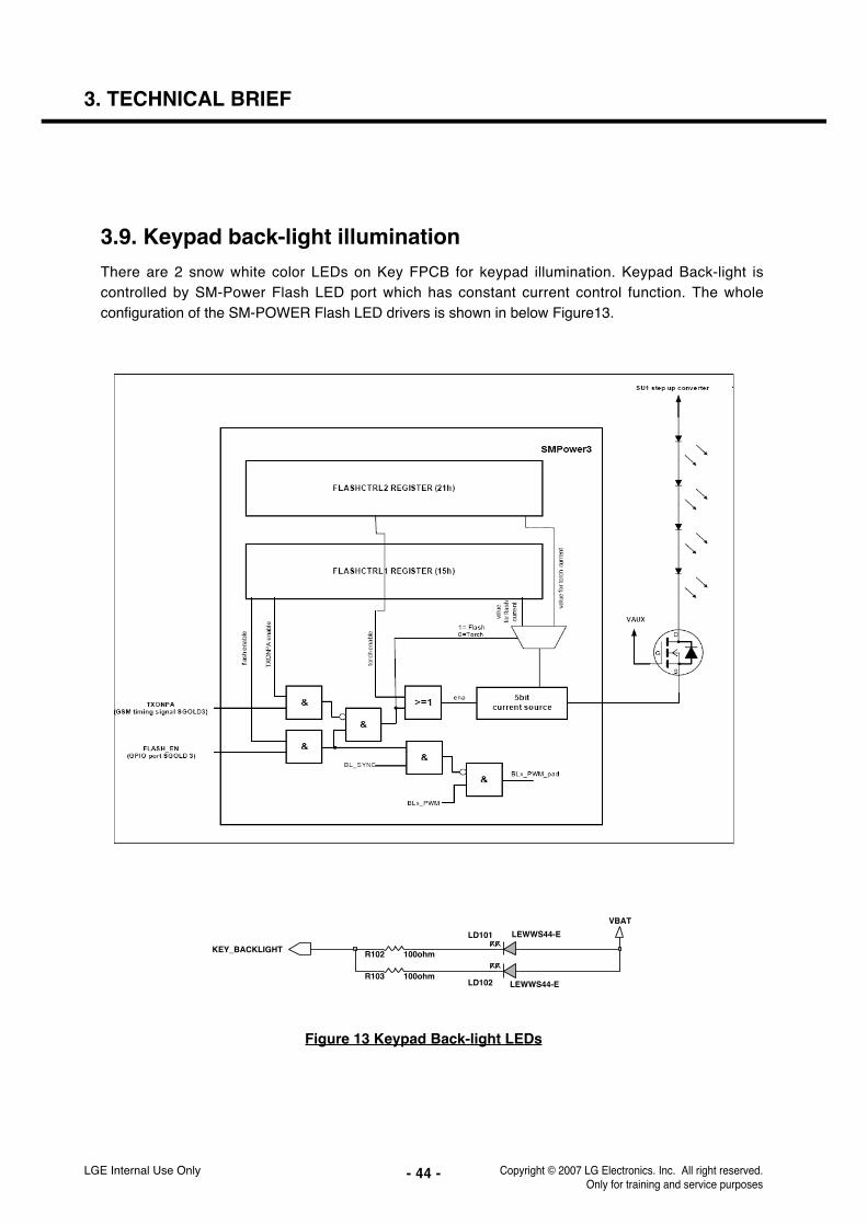
3.9. Keypad back-light illumination
There are 2 snow white color LEDs on Key FPCB for keypad illumination. Keypad Back-light iscontrolled by SM-Power Flash LED port which has constant current control function. The wholeconfiguration of the SM-POWER Flash LED drivers is shown in below Figure13.
LGE Internal Use Only Copyright © 2007 LG Electronics. Inc. All right reserved. Only for training and service purposes
Figure 13 Keypad Back-light LEDs
LD102 LEWWS44-E
LEWWS44-ELD101
R103 100ohm
VBAT
100ohmR102KEY_BACKLIGHT

- 45 -
3. TECHNICAL BRIEF
3.10. LCD back-light illumination
AAT2842 is a dual charge pump designed to support both the white LED backlight and flashapplications for systems operating with lithium-ion/polymer batteries. And AAT3151 support 3 whiteLEDs. The AAT2842 is capable of driving up to three LEDs at a total of 120mA(AAT3151 90mA). Thecurrent sinks may be operated individually or in parallel for driving higher current LEDs. To maximizepower efficiency, the charge pump operates in 1X, 1.5X, or 2X mode, where the mode of operation isautomatically selected by comparing the forward voltage of each LED with the input voltage
The interface relies on the number of rising edges of the EN/SET pin to address and load the registers.S2Cwire latches data or address after the EN/SET pin has been held high for time TLAT. The interfacerecords rising edges of the EN/SET pin and decodes them into 16 different states, as indicated in table
LGE Internal Use OnlyCopyright © 2007 LG Electronics. Inc. All right reserved. Only for training and service purposes
Figure 15 LCD Back light unit and Flash LED charge pump IC
R24
8
280K
ohm
C27
9
2.2u
820k
R24
9
1V8_EXT
R24662K
R250 120K
10KR244
R241100K
C2832.2u
C27
41u
C2872.2u
7FBB
24FENS
FL12322
FL2FL3
21
FL420
FSET3
9IN1IN2
18
14OUT
11OUTA
8OUTB
19P
GN
D
6REF
AG
ND
4
BENS25
BL1128
BL2BL3
2726
BL4
2BSET
C1+
13 12C
1-
16C
2+ C2-
17
5CT
ENL15
EP
29
FBA10
AAT2842IBJ-EE-T1U210
0.1u
C28
5
VBAT
4.7uC278
1uC
273
120KR254
2V8_VCAM
160KR252
CAMERA_STB FLASH2
MLED
FLASH3
MAIN_BACKLIGHT
MLED1MLED2MLED3MLED4
CAM_LDO_EN
FLASH1
11D2
12D3D4
1
2EN_SET
GND9
PGND13
8VIN
VOUT5
AAT3151IWP_T1U206
C1+3
4C1-
6C2+
C2-710
D1
C2711u
VBAT
1uC272
C2771u
1uC270
100K
R23
7 SLED1SLED2SLED3
SUB_BACKLIGHT
SLED
Figure 16 EN/SET port control method

- 46 -
3. TECHNICAL BRIEF
3.11. Battery current consumption monitor
KF600 use a current monitoring function to calculate the battery capacity and the remaining time, asmonitoring current flow from the battery thru 47mohm resistor.
3.12. JTAG & ETM interface connector
In case of KF600 mass production, the JTAG & ETM interface connector will not be mount on board.That is only for developing and software debugging purpose.( It will not be mounted on massproduction PCB)
LGE Internal Use Only Copyright © 2007 LG Electronics. Inc. All right reserved. Only for training and service purposes
2.2uC259
10pC264
2.2uC260
47pC262
ZXCT1010E5TA
U204
2GNDIOUT
3
5LOAD NC
1
4VIN
47mohmR226
R23022001u
C265
VBAT
G1
G2
1
2
3
CN202
C266100p
27pC263
0.1uC258
R229 1K
VSUPPLY
BAT_ID
LOAD
Figure 17 Current monitor circuit
24
G1 G2
G3 G4
9
16
252627282930
17181920212223
1
101112131415
2345678
CN101
1V8_SD2V62_VIO
TRACEPKT5TRACEPKT6TRACEPKT7TRACECLK
PIPESTAT0PIPESTAT1PIPESTAT2
TRACESYNC
TRSTnTDI
TMSTCK
RTCKTDO
EXTRSTnTRIG_IN
TRACEPKT0TRACEPKT1TRACEPKT2TRACEPKT3TRACEPKT4
Figure 18 JTAG & ETM(Embedded Trace Module) interface connector

- 47 -
3. TECHNICAL BRIEF
3.13. ISP(Image Signal Processor)
MV9319 is high-end Image Signal Processor (ISP) supporting image sensors up to 5 mega pixels.MV9319 can be applied to various image sensor modules and camera applications. MV9319 isespecially suitable for camera phones or smart-phones with built-in MCP (Mobile CameraProcessor) or MMP (Mobile Multimedia Processor). Its powerful image processing functions such asedge enhancement, color correction, advance interpolation, Auto White Balancing significantlyincreases the quality of sensor image. Moreover, real time JPEG output mode in MV9319 makesBack-end processor easier to capture and process JPEG image. MV9319 also supports variousserial interfaces to communicate with external device flexibly. MV9319 is the best solution to createhigh image quality for camera phones demanding high performance.
LGE Internal Use OnlyCopyright © 2007 LG Electronics. Inc. All right reserved. Only for training and service purposes
Figure 15. ISP Circuit
TP302
1uC339
10R337TP303
100ohmR335
C342
0.1u
1uC355
TP304
15pC348 C349NA
C3441u15p
C346
TP306
TP301
C347NA 1u
C343
0.1uC341
2V8_VISP
1uC340
C35
0
0.1u
1V8_VISP
TP305
C35
1 1u
100o
hm
R34
4
A4
TXDF7
VDDA_2_8RXC6A7
VDDA_2_8TX
D3VDDCO
D4VDDCO_E
E5VDDIO_2_8V
VSSA_RXC5
VSSA_TXB7
VSYNCOF1
G3F3
SDO3SDO4
H4G4
SDO5
F4SDO6SDO7
F5
G8SEL1
SIMO_S_GPIO31H7
F8SMCKO
G7SOMI_S_GPIO30
SRESETD1
SS_S_SDO8H6
TCLKA8B8
TCLKBTDATA
C7C8
TDATAB
TEST_0
C3
G1NSRESET
E1PCLKO
A6RCLKRCLKB
B6
RDATAA5B5
RDATAB
E4RGVDD_1_8V
E7RXD
H8SCLK_S_SDO9
A2SCL_M_SS_M
SCL_SA3
SDA_M_MISO_MB2
B3SDA_S
SDO0F2H3
SDO1SDO2
DGND5E6
DGND6
A1GPIO10_SCLK_MGPIO11_MOSI_M
B1
H1GPIO20_PWM0GPIO21_PWM1
G2
GPIO22_PWM2H2D2
GPIO23_PWM3
GPIO24_SCLK_MH5
F6GPIO25_SS_M
GPIO26_MISO_MG6
GPIO27_MOSI_MG5
C1GPIO28_SCL_MGPIO29_SDA_M
C2
E2HSYNCO
E8MCLKNRESET
MV9319U307
AVDDD6
AVDDPD5
DGND1B4
DGND2C4
DGND3D7D8
DGND4E3 2V8_VISP
ISP_PCLK
ISP_MCLK
ISP_RX_CLKPISP_RX_CLKN
ISP_RX_DATAPISP_RX_DATAN
ISP_VSI2C2_DATA2
ISP_DATA(1)
ISP_DATA(3)
ISP_DATA(5)
ISP_DATA(7)
ISP_HS
ISP_RESET
CAM_RST
CAM_SDACAM_MCLK
PD_VCM
CAM_SCK
I2C2_CLK2
ISP_DATA(0)
ISP_DATA(2)
ISP_DATA(4)
ISP_DATA(6)

- 48 -
3. TECHNICAL BRIEF
3.14. AudioKF600 Audio signal flow diagram as following diagram.
LGE Internal Use Only Copyright © 2007 LG Electronics. Inc. All right reserved. Only for training and service purposes
BT+FMBC5
PMICPMB6821
DualDPDT
18pin
/ IO
MIC
BBPPMB8877
SPK
RCV
HPAMP
FM
Ear MIC
Figure 19 Audio signal flow diagram

- 49 -
3. TECHNICAL BRIEF
3.14.1. Audio amplifier
We use PMB6821 internal amplifier.• Battery driven 450mW differential audio amplifier for driving 8 ohm loudspeaker• Two gain stages including overdrive for ringing tones• >80dB PSRR (4kHz)
LGE Internal Use OnlyCopyright © 2007 LG Electronics. Inc. All right reserved. Only for training and service purposes
Figure 20 Audio amplifier PMIC
2.2u
C22
7
522B0
32B1
4GND
S17
S26
9VCC
U202 FSA2268TUMX8
1A1B010
1B11
2A
100pC225
100nH
L205
L204
100nH
C226100p
2V62_VIO
SPK_IN_N
SPK_IN_P
RCV_P
RCV_N EAR_N
SPK_EN
EAR_P
C21
31u
C21
50.
1u
0.1uC201
C20
52.
2u
VBAT
2.2u
C203
VBAT
2.2u
C20
4
C7
VS
S_M
ON
O
A4
VU
SB
VR
EF
EX
_MA
5B
7V
DD
_MO
NO
B5
VD
D_U
SB
MO
NO
_IN
NC
5M
ON
O_I
NP
B6
MO
NO
_OU
TN
A6
MO
NO
_OU
TP
A7
OE
_NC
4
C21
41u
VUSB
SP
K_I
N_P
SP
K_I
N_N
SP
K_O
UT
P
SP
K_O
UT
N

- 50 -
3. TECHNICAL BRIEF
3.14.2. Microphone circuit
LGE Internal Use Only Copyright © 2007 LG Electronics. Inc. All right reserved. Only for training and service purposes
Figure 22 Microphone circuit
27p 27pC107
G35
OUT1
4PWR
C109
MIC101
SP0204LE5-PB
2G1G2
3
C10827p
C102
C103 0.1u
0.1u
2.2uC104
VA103
ICV
L05
0510
1V15
0FR
VA102
ICV
L05
0510
1V15
0FR
100nHL101
L102 100nH
VMIC_P
VMIC_N
MAIN_MIC_PMAIN_MIC_N

- 51 -
3. TECHNICAL BRIEF
3.15. Multi port switch
Multi port switch has employed to decrease MMI(Multi Media Interface) connector’s pin number. USB,USART, and Headset are connected via these multi port switchs. Each pin is defined by the status ofJACK_DETECT and VBUS_USB pin. Refer to the Table 8
Table 8 Multi port switch truth table
LGE Internal Use OnlyCopyright © 2007 LG Electronics. Inc. All right reserved. Only for training and service purposes
Figure 23 Multi port switch REMOTE KEY/ USB
R326
0
VUSB
0
R328
10
9VCC
8_OE
FSUSB30UMX U303
D+3
D-5
GND4
1HSD1+
7HSD1-
2HSD2+
HSD2-6
SEL
R32
2
NA
VBAT
0.1uC317
REMOTE_ADC
USB_DP
USB_DM
JACK_DETECT REMOTE_INT
JACK_DETECT='L' JACK_DETECT='H'
Pin6 Remote Int USB_DP
Pin7 Remote ADC USB_DM

- 52 -
3. TECHNICAL BRIEF
3.16. charging circuit
ISL6299 accepts two power inputs, normally one from a USB (Universal Serial Bus) port and the otherfrom a desktop cradle. The ISL6299A features 28V and 7V maximum voltages for the cradle and theUSB inputs respectively. Due to the 28V rating for the cradle input, low-cost, large output toleranceadapters can be used safely.
LGE Internal Use Only Copyright © 2007 LG Electronics. Inc. All right reserved. Only for training and service purposes
Figure 22. Charging Circuit Diagram
R227 0
1uC268
USB_VBUS
R231
39KC2691u
10BAT
1CRDL
GND8
9ICDL
IMIN6
11PGND
USB2
7USBON
_CHG4
5_EN
3_PPR
U205 ISL6299
100K
R22
3
R232
160K
VCHG_VUSB
R22
4
100K
R228
100K 1
R225
NAC267
2V11_RTC
2V62_VIOVBAT
_PPR
ICDL
_CHG_EN
EOC

- 53 -
3. TECHNICAL BRIEF
3.17. FM radio & BLUETOOTH
• FM radioSimultaneous operation with Bluetooth
- Support of US/Europe (87.5 to 108 MHz) and Japanese (76 to 90 MHz) FM band- Wide dynamic range AGC- Soft mute and stereo blend- Adjustment-free stereo decoder and AFC- Autonomous search tuning function (up/down) with programmability (threshold setting)- RDS demodulator- Audio output available over Bluetooth audio interface or dedicated audio output- Control of FM via Bluetooth HCI or I2C- Adaptive filter to suppress narrow band interference in the FM channel
• BluetoothGeneral FeaturesThe BlueCore 5-FM BGA is a single chip radio and baseband IC for Bluetooth 2.4 GHz systemsincluding enhanced data rates (EDR) to 3Mbits/s. It includes an integrated FM receiver with stereoaudio output stage and an RDS demodulator.With the on-chip CSR Bluetooth software stack, it provides a fully compliant Bluetooth system tov2.0+EDR of the specification for data and voice communications.
LGE Internal Use OnlyCopyright © 2007 LG Electronics. Inc. All right reserved. Only for training and service purposes
Figure 23. Bluetooth / FM Radio Circuit Diagram
BLUETOOTH_CSR
6.8nHC459
820p
C45
6
470nHL407
R420560
LFB212G45BA1A220FL402
5B1
7B2
4G
1
G26
G3
8
NC1
NC_DC2
UB3
C461
R42
1
0.1u
2.2
TP406
TP404
0.01u
C437
47n
15pC449
1V5
C450
15p
TP402
C458
2.2u
2V62_VIO
C464
1000pC454
820p
C455
1000pC452
0.1uC462
1R
417
D2
VS
S_R
AD
IO_1
VS
S_R
AD
IO_2
E2
F2
VS
S_R
AD
IO_3
XTAL_INK2J2
XTAL_OUT
_RS
TF
8 J1V
RE
GIN
_L
K5
VR
EG
OU
T_H
C3
VS
S_A
NA
_1D
3V
SS
_AN
A_2
E3
VS
S_A
NA
_3F
3V
SS
_AN
A_4
G3
VS
S_A
NA
_5J3
VS
S_A
NA
_6
B6
VS
S_C
OR
E
VS
S_D
IGG
9
B2
VS
S_F
M1_
1
VS
S_F
M1_
2C
1B
4V
SS
_FM
2
H2
VS
S_L
O
G8
VS
S_P
AD
S
VS
S_P
IOC
10
K6USB_DN
J7USB_DP
K1
VD
D_A
NA
VD
D_A
UD
IOA
6
A7
VD
D_C
OR
E_1
VD
D_C
OR
E_2
H10
VD
D_F
MA
2
H1
VD
D_L
O
VD
D_P
AD
SG
10
B10
VD
D_P
IO
C2
VD
D_R
AD
IO_1
VD
D_R
AD
IO_2
G2
J6V
DD
_US
B
VR
EG
EN
AB
LE_H
H4
VR
EG
EN
AB
LE_L
H3 J5
VR
EG
IN_H
PIO
_9B
7
G1RF_NRF_P
F1
RX_ND1E1
RX_P
SP
I_C
LKH
8
K9
SP
I_M
ISO
SP
I_M
OS
IK
10J9S
PI_
_CS
A5SPKR_L
SPKR_RA4
TE
ST
_EN
C4
H6UART_CTS
H5UART_RTS
K7UART_RX
J8UART_TX
D10PCM2_SYNC
H9PCM_CLK
K8PCM_IN
PCM_OUTH7
PCM_SYNCJ10
A10
PIO
_0
A9
PIO
_1
A8
PIO
_10
PIO
_11
C6
B8
PIO
_2
PIO
_3B
9E
9P
IO_4
PIO
_5E
8F
9P
IO_6
PIO
_7F
10C5
PIO
_8
K4
AIO
_0A
IO_1
J4
AUX_DACB5
A3AU_REF
C9CLK_32K
FILT_EXTB3
A1FM_NFM_P
B1
I2C_CLKC7C8
I2C_DATA
LO_REFK3
D9PCM2_CLK
E10PCM2_IN
D8PCM2_OUT
M401BLUECORE5-FM
L40
833
nH
15pC440
NAL405
TP408TP407
TP403
TP405
C44815p
0.1u
2V65_VBT
C453
C441FEED
NC1
NC2
0.1u
ANT402
C442
2.2u
L406 33nH
TP409
C46015p
C45715p
C4652.2u
C447NA
1R
415
NA
R419
47K
R42
2
C451 220n
TP401
2V62_VIO
1V5
C463
0.01u
BT_RESETn
FM_ANT
I2S1_TX
I2S1_CLK
BT_CLK
CLK32K
UART_BT_RXUART_BT_TXUART_BT_CTSUART_BT_RTS
FM_SND_RFM_SND_L
BT
_IN
T
BT_VCXO_EN
I2S1_WA0
I2S1_RX
- 54 -
3. TECHNICAL BRIEF
Bluetooth Radio• Common TX/RX teminal simplifies external matching, eliminates external antenna switch• No external trimming is required In production• Bluetooth v2.0 + EDR Specification compliant
Bluetooth Transmitter• +6 dBm RF Transmit power with level control from on-chip 6-bit DAC over a dynamic range > 30dB• Class 2 and Class 3 support without the need for an external power amplifier or TX/RX switch.
Bluetooth Receiver• Integrated channel filters• Digital demodulator for improved sensitivity and co-channel rejection• Real time digitized RSSI available on HCI interface• Fast AGC for enhanced dynamic range• Channel classification for AFH
Synthesiser• Fully integrated synthesizer requires no external VCO varactor diode, resonator or loop filter• Compatible with crystals between 7.5 and 40MHz(in multiples of 250KHz) or an external clock
Audio• Single-ended stereo analogue output• 16-bit 48 kHz digital audio bit stream output
Baseband and Software• Internal 48Kbyte RAM, allows full speed data transfer, mixed voice and data, and full piconet
operation, including all medium rate packet types• Logic for forward error correction, header error control, access code correlation. CRC, demodulation,
encryption bit stream generation, whitening and transmit pulse shaping. Supports all Bluetooth v 2.0+ EDR features incl. ESCO and AFH
• Transcoders for A-law, u-law and linear voice from host and A-law, u-law and CVSD voice over air
Physical Interfaces• Synchronous serial interface up to 4Mbits/s for system debugging• UART interface with programmable baud rate up to 4Mbits/s with an optional bypass mode• USB v1.1 interface• I2C slave for FM• Two audio PCM interfaces (input and output)• Analogue stereo (output only)
LGE Internal Use Only Copyright © 2007 LG Electronics. Inc. All right reserved. Only for training and service purposes

- 55 -
3. TECHNICAL BRIEF
3.17.1. General Features
• Single Chip Bluetooth device for cellular applications integrating radio, baseband and memory• Fabricated in advanced low power 0.13µm CMOS technology• Very low component count (6 external components)• Ultra low power design
- Peak current 40mA for basic data rate- Peak current 45mA for enhanced data rate- Bluetooth low power mode typ. 25µA
• Multiple input clock signals supported (10-40MHz)• Supply from external voltage regulator 1.8V..3.6V 1)• Autonomous power down scenarios of Bluetooth and cellular system supported• Packages:
- P-VQFN-48 package- P-WFLGA-56 package
• Temperature range from -40°C up to 85°C• Boundary scan for interface lines via JTAG
3.17.2. Micro-Controller-Section
• ARM7TDMI-STM ARM® Processor for protocol and application software• Timers + Watchdog + Interrupt Module
3.17.3. Micro-Controller Memory
LGE Internal Use OnlyCopyright © 2007 LG Electronics. Inc. All right reserved. Only for training and service purposes
BluetoothAntenna
2.4
FMRadio
I/OROM
MMU
Processor
2.4 GHzRadio
RAM
AUDIO Drivers
XTAL
I2C
SPI
UART
PIO
PCMI2S(1)
PCMI2S(2)
USB
RFIN / OUT
Main ChipPMB8877
RF IN
Stereo Analogue
PMICPMB6821
V_BT
BlueCore-5 FM
Figure 23. Bluetooth / FM Radio Block Diagram

LGE Internal Use Only Copyright © 2007 LG Electronics. Inc. All right reserved. Only for training and service purposes
3. TECHNICAL BRIEF
- 56 -
3.18. 18pin Multi Media Interface connector
Table 11 Multi media interface pin assign
KE850 MMI
Pin Function Description
1 FM_ANT FM radio antenna / Audio ground
2 HS_MIC Headset microphone signal
3 JACK_TYPE Accessory type detect
4 HS_OUT_L Headset left sound
5 HS_OUT_R Headset Right sound
6 USB_DP /
REMOTE_INT USB/ Remote control interrupt
7 USB_DM /
REMOTE_ADC USB/ Remote control Key ADC
8 JACK_DETECT Headset detect (active low)
9 VSUPPLY Battery voltage
10 VSUPPLY Battery voltage
11 RPWRON Remote power on (active high. 2.8V)
12 VCHG Charger voltage
13 VCHG Charger voltage
14 DSR N.C.
15 VBUS_USB USB VBUS
16 TX UART TX data
17 RX UART RX data
18 GND Power GND

- 57 -
3. TECHNICAL BRIEF
LGE Internal Use OnlyCopyright © 2007 LG Electronics. Inc. All right reserved. Only for training and service purposes
12,13 : CHG
8 : JACK_D
6 : USB+/Remote_INT/TXD
14 : DSR
CLOSE TO 18PIN Connector
15 : VUSB
11 : R/ON
4 : CTS/HSO_L
2 : Headset MIC
3 : Jack type
9,10 : BATT
5 : RTS/HSO_R
17 : D/ RX
18PIN IO CONNECTOR
16 : D/ TX
7 : USB-/Remote_ADC/RXD
100nHL302
C324 24p
10K
NC1NC2
12
OUT16
7OUT2
_EN10
3_FLAG
R31
0
NCP348MTR2GU302
GATE8
9GATE_OUT
GND2
1IN1
4IN2
IN35
11
R326
0
VUSB
R319 47
0
R328
10
9VCC
8_OE
FSUSB30UMX U303
D+3
D-5
GND4
1HSD1+
7HSD1-
2HSD2+
HSD2-6
SEL
R32
2
NA
VBAT
0.1uC317
24pC309
100nHL303
47R316
ICV
L05
0510
1V15
0FR
VA
315
10K
R32
3
C332NA
C331NA
1 uFC312
2V62_VIO
100nH
FL301
ICVFP10181E301FR
GND1GND2
INOUT
L304
P1
1 2P
2
3P3
P4
45P
5
P66
C31
8
EVSC5S04F050FL303
39p
R301
NA
C310 0.1u
C302100p
R302
100K
1uC
319
R303
1M
C3010.1u
2V62_VIO
L30
1
270n
H
100nH
R31
1N
A
L307
R317 47
C333
82p
2GNDOUT
1 VCC
5
3 VIN+
VIN-4
NCS2200SQ2T2G
U301
19
2
20
21
22
3456789
CN302
1
101112131415161718
R30
810
K
R305
VCHG_VUSB
330K
R320 47
C32
010
u
C32
124
p
L30
510
0nH
0.1uC311
C31310u
2V62_VIO
USB_VBUS
R30
910
K
R332
51
C30310p
C314100p
C329 24p
100nHL309
100nH
L306
2.2KR307
EVSC5S04F050FL302
P1
1 2P
2
3P3
P4
45P
5
P66
R313 47
FB302C315
NAR318
27p 27pC316
82p
ICV
L05
0510
1V15
0FR
C334
VA
314
L308
100nH
2V5_VAUDB
R306
1.5K
R331
51
VSUPPLY
REMOTE_ADC
USB_DP
USB_DM
UART_TXUART_RX
2V5_VAUDB
HSO_L
HSO_R
JACK_DETECT REMOTE_INT
FM_ANT
HOOK_DETECT
HS_MIC_PHS_MIC_N
JACK_DETECT
DSR
RPWRON_EN
JACK_TYPE
Figure 33 MMI 18pin connector circuit
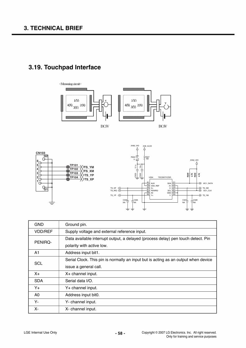
LGE Internal Use Only Copyright © 2007 LG Electronics. Inc. All right reserved. Only for training and service purposes
3. TECHNICAL BRIEF
- 58 -
3.19. Touchpad Interface
GND Ground pin.
VDD/REF Supply voltage and external reference input.
PENIRQ- Data available interrupt output, a delayed (process delay) pen touch detect. Pin
polarity with active low.
A1 Address input bit1.
SCL Serial Clock. This pin is normally an input but is acting as an output when device
issue a general call.
X+ X+ channel input.
SDA Serial data I/O.
Y+ Y+ channel input.
A0 Address input bit0.
Y- Y- channel input.
X- X- channel input.
TP103TP104
TP101TP102
G1
G2
123456
CN103
TS_XP
TS_XMTS_YP
TS_YM
C326
2V8_VLCD
NA
B2A0
A1C2
A1AUX
GNDD2
PENIRQ-B1 D1
SCL
C1SDA
VDD_REFA2A3
X+C3
X-
B3Y+
D3Y-
TSC2007IYZGRU304
NAC327
R3240
4.7K
R32
9
10u
C32
2
C32
30.
1u
2V62_VIO
R327NA
C328NA
2V62_VIO
4.7K
R33
0
C325NA
I2C1_DATA
I2C1_CLKTS_IRQ
TS_YM
TS_XM
TS_YP
TS_XP

- 59 -
3. TECHNICAL BRIEF
RF circuit
*RF Block Diagram
3.20. General Description
The RF transceiver (PMB 6272 SMARTi-PM) is an integrated single chip, quad-band transceiver forGSM850/GSM900/GSM1800/GSM1900 designed for voice and data transfer applications. Thetransceiver provides an analog I/Q baseband interface and consists of a direct conversion receiver anda quad-band polar transmitter for GSM and EDGE with integrated PGA functionality. Further on acompletely integrated SD-synthesizer with HSCSD and GPRS/EDGE capability, a digitally controlledreference oscillator with three outputs, a fully integrated quad-band RF oscillator and a three wire businterface with all necessary control circuits complete the transceiver.
LGE Internal Use OnlyCopyright © 2007 LG Electronics. Inc. All right reserved. Only for training and service purposes
Figure 34 KF600 RF part Block Diagram
RF Part BB Part
PMB6272(SMARTi PM)
SKY77340
LNA
Switch
SAW
MODE
FEM(LSHS-C085FB)
PGA
PolarModulator
/4
/2
3.8GHz
FractionalN-PLL
ADC
Sigma-DeltaModulator
Loop filter
RX 1800MHz
RX 1900MHz
TX 850/900MHz
TX 1800/1900MHz
PMB8877 (S-GOLD3)
PA_LEVEL
I/IX
Q/QX
PA_BAND
TXON_PA
VC2
VC3
AFC
RF_EN RF_DA
RF_CLK
PA_LEVEL
PA_BAND
TXON_PA
MODE
3-WireBus
interface
26MHz_MCLK
BT_CLK
Decoder
ANT_SW1
ANT_SW2
RF Control Unit
GSM Timer Unit
PMB6821(SM-Power)
RF2.85V
RF1.5V
26MHz VBAT VCTCXO
RF2.85V RF1.5V
2.85V
26MHz_MCLK
RF2.8V
VSUPPLY
PA Control
Hardware
TX 900MHz

- 60 -
3. TECHNICAL BRIEF
LGE Internal Use Only Copyright © 2007 LG Electronics. Inc. All right reserved. Only for training and service purposes
GSM850 GSM900 DCS1800 PCS1900
2V85_VRF
3OUT
VCC4
VCONT1
X401
26MHz
2GND
C4182.7p
2V85_VRF
2V85_VRF
2V85_VRF
18nH
L401
1uC446
NAC411
1uC425
C4234700p
C4330.1u
1V5_VRF
17
VDDXO2V815
XO
11 12X
OX
1000pC438
RX
3X
RX
42223
RX
4X
36TX1
37TX2
34VBIAS
VCO_RC18
31V
DD
BIA
S2V
8
8V
DD
DIG
1V5
VD
DD
IG2V
85
21V
DD
LNA
1V5
VDDMIX2V839
VDDRX1V51920
VDDRX2V8VDDTX1V535
38VDDTX2V8 VDDVCO2V8
DA
16EN
FE
132
FE233
14FSYS1
10F
SY
S2
FS
YS
39
13GND1
GN
D2
26
40GND3
GND441
29R
X1
RX
1X30 27
RX
2R
X2X
28
RX
32425
U403PMB6272
A1 2
AX
B3 4
BX
CLK
762V85_VRF
0.1uC424
0.1uC431
R414
47nC434
22
C435
1000p
10R412
0.22u
68u
C443
C412
2.2pC415C4142.2p
820R411
C4172.2p
2V85_VRF
C42627p
1.8pC420
10
R418
0.1uC422
10KR416
1V5_VRF
C4300.1u
L403
5.1nH
C419
L404
2.7p
RSVD212 5
VBATT6
VRAMP
5.1nH
13GND3
11GND4
10GND5
7GSM_IN
9GSM_OUT
1MODE
4RSVD1
DCS_PCS_IN2
16DCS_PCS_OUT
8EN
15GND1
14GND2
3BS
0.1u
1V5_VRF
C445
2.2pC416
100pC427
0.1uC444
0.1uC432
C4390.01u
R4103.3nH
R4130
C4360.22u
1.8pC421
C4100.5p
18nH
L402
AFC
LBAND_PAM_INHBAND_PAM_IN
26MHZ_MCLK
BT_CLK
RF_EN
RF_DA
RF_CLK
QX
Q
IX
I
Figure 35 RF transceiver PMB6272 SMARTi-PM functional block diagram
Figure 36 RF transceiver PMB6272 SMARTi-PM schematic

LGE Internal Use OnlyCopyright © 2007 LG Electronics. Inc. All right reserved. Only for training and service purposes
3. TECHNICAL BRIEF
- 61 -
3.21. Receiver part
The constant gain direct conversion receiver contains all active circuits for a complete receiver chainfor GSM/GPRS/EDGE (see Figure 39). The GSM850/900/DCS1800/ PCS1900 LNAs with balancedinputs are fully integrated. No inter-stage filtering is needed. The orthogonal LO signals are generatedby a divider-by-four for GSM850/900 band and a divider-by-two for the DCS1800/PCS1900 band.Down conversion to baseband domain is performed by low/high band quadrature direct downconversion mixers.The baseband chain contains a LNB (low noise buffer), channel filter, output buffer and DC-offsetcompensation. The 3rd order low pass filter is fully integrated and provides sufficient suppression ofblocking signals as well as adjacent channel interferers and avoids anti-aliasing through the basebandADC. The receive path is fully differential to suppress on-chip interferences. Several gain steps areimplemented to cope with the dynamic range of the input signals. Depending on the baseband ADCdynamic range, single-or multiple gain step switching schemes are applicable. Furthermore anautomatic DC-offset compensation can be used (depending on the gain setting) to reduce the DC-offset at baseband-output. A programmable gain correction can be applied to correct for front end- andreceiver gain tolerances.
Figure 37 Receiver part block diagram

LGE Internal Use Only Copyright © 2007 LG Electronics. Inc. All right reserved. Only for training and service purposes
3.22. Transmitter part
The GMSK transmitter supports power class 4 for GSM850 and GSM900 as well as power class 1 forDCS1800 and PCS1900. The digital transmitter architecture is based on a very low power fractional-NSigma-Delta synthesizer without any external components (see Figure39). The analog I/Q modulationdata from the baseband is converted to digital, filtered and transformed to polar coordinates. Thephase/frequency signal is further on processed by the Sigma-Delta modulation loop. The output of itsassociated VCO is divided by four or two, respectively, and connected via an output buffer to theappropriate single ended output pin. This configuration ensures minimum noise level. The 8PSKtransmitter supports power class E2 for GSM850 and GSM900 as well as for DCS1800 and PCS1900.The digital transmitter architecture is based on a polar modulation architecture, where the analogmodulation data (rectangular I/Q coordinates) is converted to digital data stream and is subsequentlytransformed to polar coordinates by means of a CORDIC algorithm. The resulting amplitudeinformation is fed into a digital multiplier for power ramping and level control. The ready processedamplitude signal is applied to a DAC followed by a low pass filter which reconstructs the analogamplitude information.The phase signal from the CORDIC is applied to the Sigma-Delta fractional-N modulation loop. Thedivided output of its associated VCO is fed to a highly linear amplitude modulator, recombiningamplitude and phase information. The output of the amplitude modulator is connected to a singleended output RF PGA for digitally setting the wanted transmit power. The PA interface of SMARTi-PMsupports direct control of standard dual mode power amplifiers (PA’s) which usually have a powercontrol input VAPC and an optional bias
3. TECHNICAL BRIEF
- 62 -
Figure 38 Transmitter part block diagram

LGE Internal Use OnlyCopyright © 2007 LG Electronics. Inc. All right reserved. Only for training and service purposes
3. TECHNICAL BRIEF
- 63 -
control pin VBIAS for efficiency enhancement. In GMSK mode, the PA is in saturated high efficiencymode and is controlled via its VAPC pin directly by the baseband ramping DAC. In this way both up- /down-ramping and output power level are set. In 8PSK mode, the ramping functionality is assured byan on-chip ramping generator, whereas output power is controlled by the PGA’s as described above.
3.23. RF synthesizer
The transceiver contains a fractional-N sigma-delta synthesizer for the frequency synthesis in the RXoperation mode. For TX operation mode the fractional-N sigma-delta synthesizer is used as Sigma-Delta modulation loop to process the phase/frequency signal. The 26MHz reference signal is providedby the internal crystal oscillator. This frequency serves as comparison frequency of the phase detectorand as clock frequency for all digital circuitry.The divider in the feedback path of the synthesizer iscarried out as a multi-modulus divider (MMD). The loop filter is fully integrated and the loop bandwidthis about 100 kHz to allow the transfer of the phase modulation. The loop bandwidth is automaticallyadjusted prior to each slot (OLGA2). To overcome the statistical spread of the loop filter element valuesan automatic loop filter adjustment (ALFA) is performed before each synthesizer startup. The fullyintegrated quad-band VCO is designed for the four GSM bands (850, 900, 1800, 1900 MHz) andoperates at double or four times transmit or receive frequency. To cover the wide frequency range theVCO is automatically aligned by a binary automatic band selection (BABS) before each synthesizerstartup.
3.24. VCTCXO
The VCTCXO (X401) supply 26MHz reference clock and controlled by AFC input to generate a strictsystem clock. The 26MHz clock is used to Transceiver(U403), Bluetooth chip(U402) and S-Gold2(U101).
3OUT
VCC4
VCONT1
X401
26MHz
2GND
2V85_VRF
1uC446
XO
11 12X
OX
1000pC438
13GND1
R41422
10KR416
0.1uC445
C4390.01u
AFC
Figure39 VCTCXO Schematic

LGE Internal Use Only Copyright © 2007 LG Electronics. Inc. All right reserved. Only for training and service purposes
3. TECHNICAL BRIEF
- 64 -
3.25. Front End Module control
Implemented in the S-Gold3 (FL401) are three outputs which are FE1, FE2 for direct control of frontend modules with two logic input pins to select RX and TX mode as well as low and high bandoperation.
Table 12 FEM Control Logic
Figure 40 FEM schematic
MODE Tx 1GHz Tx 2GHz Rx GSM Rx EGSM Rx DCS TX PCS
VDD ON ON ON ON ON ON
VC1 ON OFF OFF OFF OFF OFF
VC2 OFF ON OFF OFF OFF OFF
H
L
PIN 14
L
L
L
DCS1800 RX
EGSM900 RX
L
L
L
VC2VC1
DCS_PCS TX
PCS1900 RX
L L
GSM850 RX L
PIN 13
GSM850_EGSM TX H
R40
5N
A
C402100p
2V85_VRF
100pC401
DNIR408
100ohm
A1
A2
GNDVCC
Y1
Y2
R401
NC7WV16P6X U401
C406NA
22pC404
100nHC405
GS
M85
0RX
_OU
T1
2G
SM
850R
X_O
UT
2
17G
SM
850_
900_
TX
GS
M90
0RX
_OU
T1
3 4G
SM
900R
X_O
UT
2
NC
2119V
C1
VC
220
ANT
GN
D1
9
GN
D10
24
GN
D2
10 12G
ND
3G
ND
413
GN
D5
14
GN
D6
16 18G
ND
722
GN
D8
GN
D9
23
5G
SM
1800
RX
_OU
T1
6G
SM
1800
RX
_OU
T2
15G
SM
1800
_190
0_T
X
GS
M19
00R
X_O
UT
17 8
GS
M19
00R
X_O
UT
2
1
LSH
S-C
085F
BF
L401
11NAC407
C4031000p
R402100ohm
RF-800SW401
ANTG1
G2RF
FE2
FE1

- 65 -
3. TECHNICAL BRIEF
3.26. Power Amplifier Module
The SKY77340 (U402) designed in a compact form factor for quad-band cellular handsets comprisingGSM850/900,DCS1800,PCS1900, supporting GMSK and linear EDGE modulation. The moduleconsists fo a GSM850/900 PA block and a DCS1800/PCS1900 PA block, impedance-matchingcircuitry for 50 ohms input and output impedances, and a Multi-function Power Amplifier Control(MFC)block. Two separate Heterojunction Bipolar Transistor9HBT) PA blocks are fabricated onto InGaP die.One supports the GSM850.900 bands, the other supports the DCS1800 and PCS1900 bands. BothPA blocks share common power supply pins to distribute current. RF input and output ports areinternally matched to 50 ohms to reduce the number of external components.
Table 13 PAM pin description
LGE Internal Use OnlyCopyright © 2007 LG Electronics. Inc. All right reserved. Only for training and service purposes
PIN Name Description
1 MODE GMSK/EDGE Power control mode. L=GMSK, H=EDGE
2 DCS/PCS_IN RF input(DCS/PCS) DC Blocked
3 BS Band Select
4 REVD1 Reserved
5 VBATT DC Supply
6 VRAMPAnalog PA Bias Control(All Bands, EDGE Mode)
Analog Output Power Control(All Bands, GMSK Mode)
7 GSM_IN RF input(EGSM) DC Blocked
9 GSM_OUT RF Output(EGSM) DC Blocked
10,11 GND Ground
12 REVD2 Reserved
13,14,15 GND Ground
16 DCS/PCS_OUT RF Output(DCS/PCS) DC Blocked
Pad GND PAD GRID Ground pad grid is device underside.

LGE Internal Use Only Copyright © 2007 LG Electronics. Inc. All right reserved. Only for training and service purposes
3. TECHNICAL BRIEF
- 66 -
3.27. Mode Selection
Table 14 Mode Selection
MODE circuitry selects GMSK modulation (logic 0) or EDGE modulation (logic 1).VRAMP controls the output power for GMSK modulation and provides bias optimization for EDGEmodulation depending on the state of MODE control.
3.28. PAM Schematic
MODE VMODE RF INPUT VRAMP TX ENABLE
GSM Low Fixed Vramp control output Power High
EDGE High Ramp Burst Control Vramp sets PA bias condition, fixed gain PA High
C408NA
NAC411
1uC425
820pC429
0.1uC424
VSUPPLY
100pC413
68u
DNI
C412
R408
1.2KR409
C42627p
C428100p
NAC409
RSVD212 5
VBATT6
VRAMP
31GND21
30GND22GND23
2928
GND2427
GND25
13GND3
11GND4
10GND5
GND617
GND71819
GND8GND9
20
7GSM_IN
9GSM_OUT
1MODE
4RSVD1
DCS_PCS_IN2
16DCS_PCS_OUT
8EN
15GND1
GND1021
GND1122
GND1223
GND1324
GND142526
GND15
GND1636
GND1735
GND1834
GND1933
14GND2
GND2032
U402SKY77340
3BS
100pC427
R4103.3nH
C4100.5p
PA_LEVELLBAND_PAM_IN
HBAND_PAM_IN
TXON_PA
PA_MODE
PA_BAND
Figure 41 PAM schematic
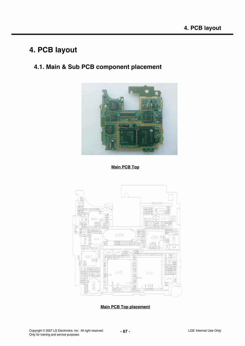
LGE Internal Use OnlyCopyright © 2007 LG Electronics. Inc. All right reserved. Only for training and service purposes
4. PCB layout
- 67 -
4. PCB layout
4.1. Main & Sub PCB component placement
Main PCB Top
Main PCB Top placement

LGE Internal Use Only Copyright © 2007 LG Electronics. Inc. All right reserved. Only for training and service purposes
4. PCB layout
- 68 -
Main PCB bottom
Main PCB bottom placement

LGE Internal Use OnlyCopyright © 2007 LG Electronics. Inc. All right reserved. Only for training and service purposes
4. PCB layout
- 69 -
Battery Connector
Charging IC
Bluetooth & FM radio Chip
Bluetooth Antenna
Camera Connector
Sleep Crystal
BBP
Mobile Switch
Memory
PMIC
SIM & uSD Socket
RF Block
Flash LED
Power Inductor
Power Inductor
Camera ISP Chip
SUB Charge pump
MAIN Charge pump
Key FPCB Conn.
64 PIN Conn.
Vibrator PAD
Ear phone AMP OVP
Vibrator Driver IC
Touch IC

LGE Internal Use Only Copyright © 2007 LG Electronics. Inc. All right reserved. Only for training and service purposes
4. PCB layout
- 70 -
Hall IC
Volume Up
Volume Down
MP3 Key
AF Camera Key
Microphone
KEY Backlight LED
MP3/Camera KEY
ReceiverTouch Conn. Backup Battery
LCD Connector
64PIN Connector
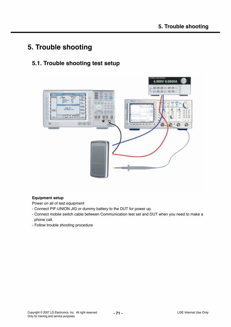
LGE Internal Use OnlyCopyright © 2007 LG Electronics. Inc. All right reserved. Only for training and service purposes
5. Trouble shooting
- 71 -
5.1. Trouble shooting test setup
Equipment setupPower on all of test equipment- Connect PIF-UNION JIG or dummy battery to the DUT for power up.- Connect mobile switch cable between Communication test set and DUT when you need to make a
phone call.- Follow trouble shooting procedure
5. Trouble shooting

LGE Internal Use Only
5.2. Power on Trouble
Check Points-Battery Voltage( Need to over 3.35V)-Power-On Key detection (PWRON signal)-Outputs of LDOs from PMIC
Copyright © 2007 LG Electronics. Inc. All right reserved. Only for training and service purposes
5. Trouble shooting
- 72 -
10uC275
R233100K
2V11_RTC
100K
R236
R235
10KR234 0
PWRON
RPWRON_ENRPWRON
END_KEY_IN
A2 3
B16
B2 2
GND4
VCC 8
Y1 1
Y25
U208NC7WZ08L8X
A17
2V11_RTC
R23
9
100K
C2820.1u
2V62_VIO
EXTRSTnSPOWER_INT PM_INT
PMRSTn_RESET
TP1
TP2

LGE Internal Use OnlyCopyright © 2007 LG Electronics. Inc. All right reserved. Only for training and service purposes
5. Trouble shooting
- 73 -
PMIC2V62_VIO
0.1uC236
VBAT
C23
210
u
TP202
NAR202
0.1u
C21
2
C2400.1u
4.7K
R20
7
C2472.2u
C2282.2u
C21
31u
C2301u
10uHL201
22u
1V35_CORE
C237
0R213
C21
12.
2u
R20
40
EX
T_O
N
2V5_VAUDB
2V9_SIM2V11_RTC
R21
14.
7K
C21
5
VBAT
0.1u
R20
9N
A
2.2uC241
1uC245
2V5_VAUDA
R21
210
0K
100u
PMRSTn
VBAT
C206
C2392.2u 2.2u
C2482.2u1uC249C243
FB
201
2V85_AMP
2.2uC246C242
2.2u
4.7K
R20
8
VBAT
C21
02.
2u
1V8_SD
R21
04.
7K
U_VMIN
10u
C23
1
KD
S16
0E
2V85_VRF
D20
2
0.1uC201
C20
52.
2u
4.7K
C251
R20
6
2V8_VMME
2.2u
VBAT
VCHG_VUSB
2.2u
C203
C23510u
VBAT D20
1
KD
S16
0E
2.2uC202
SP
_IN
T
U_RCV
C2441u
VBAT
2.2uC250
2V8_VLCD1V8_SD
2.2u
C20
4
VVIBF11
WD
OG
L3
10uC234 H
6V
SS
28V
SS
29H
7
D5
VS
S3
J6V
SS
30
VS
S4
D6
D7
VS
S5
VS
S6
D8
E4
VS
S7
VS
S8
E5
E6
VS
S9
C7
VS
S_M
ON
O
VS
S_S
D1
H8
H4
VS
S_S
D2
D9
VS
S_V
RE
F
J11VUMTS
A4
VU
SB
F3
VS
S13
VS
S14
F4
F5
VS
S15
VS
S16
F6
F7
VS
S17
VS
S18
F8
F9
VS
S19
VS
S2
D4
VS
S20
G3
G4
VS
S21
VS
S22
G5
VS
S23
G6
G7
VS
S24
VS
S25
G8
G9
VS
S26
VS
S27
H5
C11VMME
C2VPIN
VP
LLA
10
VR
EF
C8
VR
EF
EX
_MA
5
F10VRF1
VRF2D11
E10VRF3
VRTCH10
VS
D1
L11
VS
D2
L1
VSIMG10
C6
VS
S1
VS
S10
E7
E8
VS
S11
VS
S12
E9
VDDAUXH1
VDDMMEC10
B9
VD
DP
LLIO
VDDRF13_AFCE11
D10VDDRF2
VDDSD1K11
VDDSD2K1
G11VDDSIMVIB
VDDUMTSH9
K9
VD
D_C
HA
RG
E
B7
VD
D_M
ON
O
VD
D_R
EF
J9B5
VD
D_U
SB
A11
VIO
A8
VLE
D
VMIND3
SE
NS
E_I
N1
L9 K10
SE
NS
E_I
N2
E2SLEEP1_NSLEEP2_N
E1
H3SU1_FB
J1SU1_GATESU1_GND
J2
SU1_ISENSEJ3
A3
SU
SP
EN
D
TX
ON
PA
B10
H11VAFC
F2VAUDIOA
VAUDIOBG1
H2VAUX
VDDAUDIOAF1
G2VDDAUDIOB
L5O
N_O
FF
_OU
T
OU
TP
OR
TJ4 K
3P
OW
ER
_ON
A1
PU
MS
1P
UM
S2
B4
B11
PU
MS
3
RCVB1
RESET2_ND1E3
RESET_N
RE
SO
UR
CE
_CR
TL
J5B8
RR
EF
J10SD1_FB
SD1_FBLL10K2
SD2_FBSD2_FBL
L2
B2
SE
0_V
M
K8
CH
_SO
UR
CE
C1D+D-
D2
DA
T_V
PA
2
C9
FLA
SH
_ON
FLA
SH
_SH
INK
A9
J7I2
C_C
LKI2
C_D
AT
K6
K5
I2C
_IN
T
MO
NO
_IN
NC
5M
ON
O_I
NP
B6
MO
NO
_OU
TN
A6
MO
NO
_OU
TP
A7
OE
_NC
4
K4
ON
_OF
F1
ON
_OF
F2
L4
PMB6821U203
B3
AC
+A
C-
C3
L6B
L1_P
WM
BL2
_PW
MK
7J8
BL3
_PW
M
CH
AR
GE
_UC
L8
CH
_CN
TR
LL7
TP201
FB202
C21
4
VBAT
1u
2V62_VIO
R201
27K
2.2uC229
1V5_VRFC
209
1u
2V65_VBT
L206
10uH
C21
81u
2V9_VAF
C2382.2u
C23
310
u
1V35_VPLL
U_PMIN
VUSB
VBAT
_PP
R
PW
RO
N
KE
Y_B
AC
KLI
GH
TK
EY
_EN
SP
K_I
N_P
SP
K_I
N_N
SP
K_O
UT
P
SP
K_O
UT
N ON
_OF
F2
ON_OFF2RTC_OUT
WD
OG
PMRSTn
VCXO_ENBT_VCXO_EN
TXON_PA
USB_SE0_VM
USB_DPUSB_DM
I2C
1_C
LKI2
C1_
DA
TA
SP
OW
ER
_IN
T
USB_OEn
RE
SO
UR
CE
_CT
RL
USB_DAT_VP
LDO Net name Output Voltage Output Current Usage
SD1 1V35_Core 1.35V 600mA Core & for LDO
SD2 1V8_SD 1.8V 300mA Memory
VAUX 2V9_VAF 2.9V 100mA Cam Auto Focus
VIO 2V62_VIO 2.62V 100mA Peripherals
VSIM 2V9_SIM 2.9V 70mA SIM card
VMME 2V8_VMME 2.9V 150mA u-SD
VUMTS 2V85_AMP 2.85V 110mA Headset AMP
VUSB VUSB 3.1V 40mA Not used
VLED VLED 2.9V 10mA Not used
VAUDIOa 2V5_VAUDA 2.5V 200mA Stereo headset, Mono earpiece
VAUDIOb 2V5_VAUDB 2.5V 50mA Analog parts of S-Gold
VRF1 2V85_VRF 2.85V 150mA 2.85 V supply for SMARTi-PM RF transceiver
VRF2 1V5_VRF 1,53V 100mA 1.5 V supply for SMARTi-PM RF transceiver
VRF3 2V65_VBT 2.7V 150mA Bluetooth
VPLL 1V35_VPLL 1.35V 30mA S-GOLD3 PLL
VRTC 2V11_RTC 2.11V 4mA Real Time Clock
VAFC VAFC 2.65V 5mA Not used
VVIB 2V8_VLCD 2.8V 140mA LCD

LGE Internal Use Only Copyright © 2007 LG Electronics. Inc. All right reserved. Only for training and service purposes
5. Trouble shooting
- 74 -
14pin of U403
START
ìPWRONî s ignal Check 3 pin of Q201
ì_ RESETî s ignal Check 5 pin of U208
Check the all LDOís output
Is it correct?
Is the 26MHz clock From U403
signal correct?
Replace main PCB
Check the RPWRON,
replace Q201
Check solder U208 or replace it
Check solder U203 or replace it
Check solder X401, U403 or replace it
Check 3 pin of X401
Or Check 14 pin of U403
Yes
Yes
Yes
Yes
Yes
No
No
No
No
Connect power supply to the DUT Vbat = over 3.35V
Q201
TP1
TP2
U208
U203
X401
3pin of X401U403

LGE Internal Use OnlyCopyright © 2007 LG Electronics. Inc. All right reserved. Only for training and service purposes
5. Trouble shooting
- 75 -
5.3. Charging trouble
Check Points-Connection of TA (check TA voltage 4.8V)-Charging Current Path component voltage drop-Battery voltage
1 Charging method: CC-CV2 Charger detect voltage: 4.0 V3 Charging time: 2h 30m4 Charging current: 600 mA5 CV voltage: 4.2 V6 Cutoff current: 110 mA7 Full charge indication current (icon stop current): 110 mA8 Recharge voltage: 4.16 V
R227 0
1uC268
USB_VBUS
R231
39KC2691u
10BAT
1CRDL
GND8
9ICDL
IMIN6
11PGND
USB2
7USBON
_CHG4
5_EN
3_PPR
U205 ISL6299
100K
R22
3
R232
160K
VCHG_VUSB
R22
4
100K
R228
100K 1
R225
NAC267
2V11_RTC
2V62_VIOVBAT
_PPR
ICDL
_CHG_EN
EOC
4.2V~3.69V 3.69V~3.53V 3.53V~3.43V 3.43V~3.3V
TP1 TP2

LGE Internal Use Only Copyright © 2007 LG Electronics. Inc. All right reserved. Only for training and service purposes
5. Trouble shooting
- 76 -
START
18pin IO(CN302) Is soldered ?
Source pin (1) of U205 =
4.8V ?
Output pin (10) of U205 =4.2V?
Resolder the CN302
Battery voltage is over 3.4V?
Charge is operating
The TA can be broken
Change other TA then retest
Check solder U205 or replace it
Waiting until battery
Voltage goes up to 3.4V
Yes
Yes
Yes
Yes
Yes
No
No
No
No
Battery thermistor value
is about 10K?
Change the Battery retest
No
18pin IO(CN302)
U205 TP1: Source pin(1)
U205 TP2: Output
pin(10)
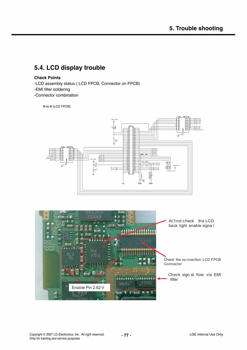
LGE Internal Use OnlyCopyright © 2007 LG Electronics. Inc. All right reserved. Only for training and service purposes
5. Trouble shooting
- 77 -
5.4. LCD display trouble
Check Points-LCD assembly status ( LCD FPCB, Connector on FPCB)-EMI filter soldering-Connector combination
B-to-B (LCD FPCB)
2V11_RTC
R34
310
K100nHL310
0.1uC338
2V8_VLCD
capa
cito
r
C352NA
R33
3
0
10K
R34
2
109
OUT8
PG
ND
17
1IN1IN2
2
IN33
IN44
IN556
IN67
IN7IN8
8
16OUT1
15OUT2
14OUT3OUT4
13
OUT51211
OUT6OUT7
CM1431-08FL305
27p
C35
427
pC
353
R34
010
K
4.7K
R341
1uC345
2V8_VLCD
51525354
6789
G1 G2
G3 G4
373839
4
40414243444546474849
5 50
222324252627 28
29
3
30313233343536
1
10111213141516171819
2
2021
CN304
L311 100nH
NAR336
16OUT1
15OUT2
14OUT3OUT4
13
OUT51211
OUT6OUT7
109
OUT8
PG
ND
17
1IN1IN2
2
IN33
IN44
IN556
IN67
IN7IN8
8
CM1431-08FL304
DIF_D(5)
DIF_D(7)
DIF_D(0)
DIF_MAIN_CS
DIF_WR
DIF_D(2)
DIF_CD
DIF_D(4)
DIF_RESET
VSYNC
DIF_D(6)
DIF_D(8)
DIF_SUB_CS
DIF_D(3)
DIF_D(1)
RCV_PRCV_N
MLED2MLED3
MLED1MLED LCD_ID
MLED4
SLED1SLED2
TS_XMTS_XP
SLED
SLED3
TS_YPTS_YM
At f irst check the LCD back light enable signa l
Check sign al flow via EMI filter
Check the co nnection LCD FPCB Connector
Enable Pin 2.62 V

- 78 -
5. Trouble shooting
LGE Internal Use Only Copyright © 2007 LG Electronics. Inc. All right reserved. Only for training and service purposes
START
Is LCD FPCB normal?
Signal is normal on 2.62V Signal FL304, FL305
Assemble
Replace LCD FPCB
Check solder and repair
Damaged filter
Yes
Yes
No
No
Check LCD connector combination then LCD test
with New LCD
FL304 FL305

- 79 -
5. Trouble shooting
LGE Internal Use OnlyCopyright © 2007 LG Electronics. Inc. All right reserved. Only for training and service purposes
5.5. Camera Trouble
Check Points-Connectors combination-FPCB status
B-to-B (3M Camera Sensor)
R31
5
4.7K
ICV
L050
5101
V15
0FR
VA301
FB301C30415p
1V8_EXT
1V8_EXT
2V8_VCAM
1uC306
6789
G1 G2
G3 G410 11
1213141516171819220
345
CN301
1
C3080.1u
R304 100ohm
15pC305
2V9_VAF
0.1uC307
R31
4
4.7K
VA302
ICV
L050
5101
V15
0FR
PD_VCMCAM_RST
CAM_MCLK
ISP_RX_CLKNISP_RX_CLKP
ISP_RX_DATANISP_RX_DATAP
CAM_SCKCAM_SDA
Check the connector combination

LGE Internal Use Only Copyright © 2007 LG Electronics. Inc. All right reserved. Only for training and service purposes
5. Trouble shooting
- 80 -
START
Replace New Camera module
Working properly?
Assemble
Yes
Yes
No
Check camera connector, 34pin main PCB connector combination then Camera test with equipped camera module
Replace Camera module
Yes
Replace Main PCB

LGE Internal Use OnlyCopyright © 2007 LG Electronics. Inc. All right reserved. Only for training and service purposes
5.6. Receiver & Speaker trouble
Check Points-Speaker pin contact-Audio amp soldering-analog switch soldering
5. Trouble shooting
- 81 -
Check Input signal, HP AMP 1.6V
Check Analog SW, Input si gnal 1.6V
Check the Analog SW
Check Analog S W, Output signal 1.6V
TP1
TP2
TP5 TP6
TP3
TP4
TP3
TP4
2.2u
C22
7
522B0
32B1
4GND
S17
S26
9VCC
U202 FSA2268TUMX8
1A1B010
1B11
2A
100pC225
100nH
L205
L204
100nH
C226100p
2V62_VIO
SPK_IN_N
SPK_IN_P
RCV_P
RCV_N EAR_N
SPK_EN
EAR_P
HP AMP & SPK
22KR205
2V85_AMP
2.2uC221
C1N
C4
C1P
A4
C1INL
A1INR
B3
NC
1C
3N
C2
OUTLD2
OUTRC2
PGNDB4
A3PVDD PVSS
D4
SGNDA2
D1SVDD
D3SVSS
_SDLB2B1
_SDR
U201 TPA4411YZH
22KR203
C220 2.2u
C2192.2u
C21668p
C207 1u
22KR276
22KR275
C208 1u
C21768p
BB_SND_L
BB_SND_R
FM_SND_RFM_SND_L
HSO_R
_AMP_SHDN
HSO_L
TP7TP3
TP4TP8
TP1
TP2 TP5
TP6
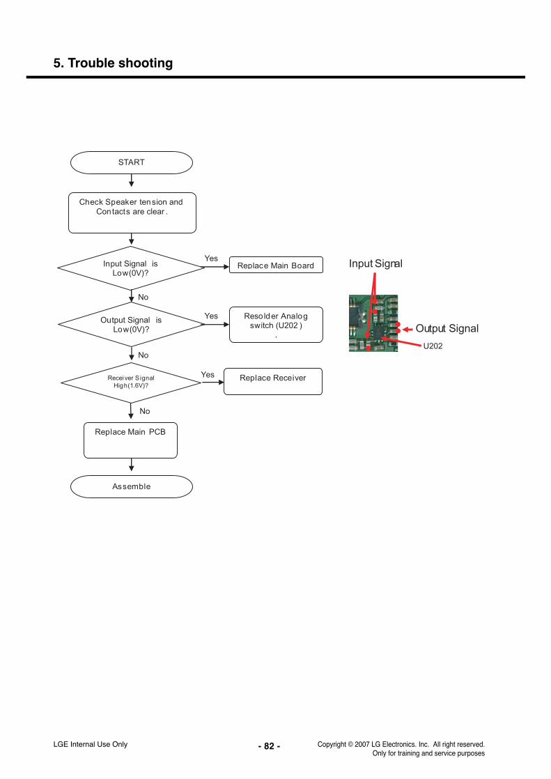
LGE Internal Use Only Copyright © 2007 LG Electronics. Inc. All right reserved. Only for training and service purposes
5. Trouble shooting
- 82 -
START
Input Signal is Low(0V)?
Output Signal is Low(0V)?
Assemble
Replace Main Board
Reso lder Analog switch (U202 )
.
No
Yes
Yes
Check Speaker tension and Contacts are clear .
No
No
Replace Main PCB
Yes Receiver Signal High(1.6V)?
Replace Receiver
U202
Input Signal
Output Signal

LGE Internal Use OnlyCopyright © 2007 LG Electronics. Inc. All right reserved. Only for training and service purposes
5. Trouble shooting
- 83 -
5.7. Microphone trouble
Check Points-Microphone hole-Mic. Bias & signal come from
27p 27pC107
G35
OUT1
4PWR
C109
MIC101
SP0204LE5-PB
2G1G2
3
C10827p
C102
C103 0.1u
0.1u
2.2uC104
VA103
ICV
L05
0510
1V15
0FR
VA102
ICV
L05
0510
1V15
0FR
100nHL101
L102 100nH
VMIC_P
VMIC_N
MAIN_MIC_PMAIN_MIC_N
START
Mic bias ON (2.5V)when call?(C103)
20pin connector is good?
Assemble
Check mic. Bias line
Repair the 20pin conn. (CN303)
Yes
No
No
Check microphone sound hole
Check Signal C101, C102 (2.5V)
Replace microphone
(MIC100)
Yes
No
Mic bias(C103)
C101 C102
MIC100
CN303

LGE Internal Use Only Copyright © 2007 LG Electronics. Inc. All right reserved. Only for training and service purposes
5. Trouble shooting
- 84 -
5.8. Vibrator trouble
Check Points-Vibrator soldering-IC is working correct
GND
IN
OUT
-
+
VIBRATOR1KR24
2 5.1K
R24
0
51KR245
3VOUT
R1114D311DU207
CE6
2GND1
5GND2
4NC
VDD1
C2861uR251 0
1uC
280
Q203
KRC402E
B
C
E
51KR243
TPA6205A1ZQVRU209
BYPASSC1
GNDB2
C2IN+
C3IN-
A3VDD
VO+B3
VO-A1B1
_SHUTDOWN
VBAT
C276 0.01u
R253 100K
100nHL207
L208100nH
0.1u
C284
R238 110K
VIBN
VIBP
910
R24
7
1uC281
VIB_PWM
VIB_EN
Check t he sol dering is clear, if th ere is some obst acles re- solder
Check the dri ver IC(U209) PWM Signal
TP3
TP1TP2
TP3

LGE Internal Use OnlyCopyright © 2007 LG Electronics. Inc. All right reserved. Only for training and service purposes
5. Trouble shooting
- 85 -
START
Pin1(VBAT) of U207(3.1V) and Pin3 is
high?
Check PWM Signal (TP3) is OK?
Assemble
Check U207 or replace it
Check Q203 or replace it
Yes
No
No
Check Vibrator sodering
Replace Vibrator
Yes
TP1 TP2
U207
TP3
Q203

LGE Internal Use Only Copyright © 2007 LG Electronics. Inc. All right reserved. Only for training and service purposes
5. Trouble shooting
- 86 -
5.9. Keypad back light trouble
Check Points-Signal path is connected well-Analog SW is working properly
LD102 LEWWS44-E
LEWWS44-ELD101
R103 100ohm
VBAT
100ohmR102KEY_BACKLIGHT
VA
310
VA
306
C3302.2uV
A30
4
VA
312
VA
305
ICVL0505101V150FR
VA
303
VA
311
VA
307
2V62_VIO
VA
308
VA
309
VA313ICVL0505101V150FR
8
9
G1
G2
VBAT
12
13
14
15
16
17
18
192
20
3
4
5
6
7
CN303
1
10 11SLIDE_DETECT
KP_IN(0)
KEY_BACKLIGHT
KP_OUT(3)
KP_OUT(2)
KP_OUT(1)
KP_OUT(0)
KP_IN(4)
KP_IN(3)
KP_IN(2)
KP_IN(1)
END_KEY
VMIC_P
VMIC_N
MAIN_MIC_P
MAIN_MIC_N
TP

LGE Internal Use OnlyCopyright © 2007 LG Electronics. Inc. All right reserved. Only for training and service purposes
5. Trouble shooting
- 87 -
START
Check CN303 TP is 2.62V?
20pin connecto r (CN303) is good?
Assemble
Check U203 or U102 rep lace Board
Replace 20pin conn.
(CN303)
Yes
No
No
Check All o f LEDs so lder
Replace KEY FPCB
Yes
CN303 U203
U102
TP

LGE Internal Use Only Copyright © 2007 LG Electronics. Inc. All right reserved. Only for training and service purposes
5.10. SIM & uSD trouble
SIM Check Points-Power is working-Socket soldering-Proper SIM is used
5. Trouble shooting
- 88 -
SIM & MMC Connetor
SW201SPVM110200
1 2
3 4
NAC257
100K
R21
6
C253NA
2V9_SIM
R21
4
4.7K
100K
R22
0
1000pC261
R21
5
100K
2V62_VIO
2V62_VIO
100K
R21
9
47
R221
1uC254
1uFC252
45
T4T5
67
T6T7
8
T89
19G
1G
220
G3
21
S1
16
S2
1412S
3
S41
15S
5
13S
6
S7
11
10S8
17ST1ST2
18
2T1
3T2T3 S
201
R222
100K
27pC256
27pC255
2V8_VMME
100K
R21
8
R21
7
100K
MMC_DETECT
MMC_CLK
SIM_DETECT
SIM_RSTSIM_CLK
SIM_IO
MMC_D(3)
MMC_D(1)MMC_D(0)
MMC_CMD
MMC_D(2)
Check sol dering all pin of socket 11
12 13

LGE Internal Use OnlyCopyright © 2007 LG Electronics. Inc. All right reserved. Only for training and service purposes
5. Trouble shooting
- 89 -
uSD Check Points-Power is working-Socket soldering-Card detect is working
MMC-DETECT PIN
MMC_DETECT SIGNAL
TP1
TP2
TP3
TP4
START
6 pins are so ldered w ell?
Check Pro per SIM Card
Assemble
Reso lder pin
Replac e Main Board
Yes
Yes
No
Check All of SIM card voltage KF600 support
1.8V & 2.9V SIM onl y
Card insert Card eject

LGE Internal Use Only Copyright © 2007 LG Electronics. Inc. All right reserved. Only for training and service purposes
5. Trouble shooting
- 90 -
START
TF socket pins are well soldered
Check proper uSD?
Assemble
Resolder it(check data line TF dat 0,1,2,3)
Replace Main Board
Yes
Yes
No
Check Micro SD card voltage (2V8_VMME)

5.11. Touch pad trouble
Check Points- Connectors combination`- FPCB Crack
TP103TP104
TP101TP102
G1
G2
123456
CN103
TS_XP
TS_XMTS_YP
TS_YM
LGE Internal Use OnlyCopyright © 2007 LG Electronics. Inc. All right reserved. Only for training and service purposes
5. Trouble shooting
- 91 -
START
CN103 Solder check OK?
FPCB is Crack?
Replacd Main Board
Resolder it
Replace FPCB
Yes
No
No
Check Touch Signal (If not replace front touch
panel)
CN103
This fault mainly depend on Touch-panel Conn.Almost of all case, Replace LCD FPCB.

- 92 -
5. Trouble shooting
5.12. Trouble Shooting of Receiver Part
Checking Points
LGE Internal Use Only Copyright © 2007 LG Electronics. Inc. All right reserved. Only for training and service purposes
START
Check point VCTCXO
Check point PLL Control
Setup Test Equipment Cell Power : ñ74dBm
EGSM CH30 DCS CH699
Re-Download S/W & CAL
Check point RX I/Q Signal
Check point Mobile SW & FEM
Figure 2. Main PCB Bottom
Checking Flow
Checking Points

- 93 -
5. Trouble shooting
5.12.1. Checking VCTCXO Circuit
LGE Internal Use OnlyCopyright © 2007 LG Electronics. Inc. All right reserved. Only for training and service purposes
TP2(C438) : 26MHz
X401
TP1(C446) : 2.85V
Replace X401
Checking U203 (PMIC)
Yes
No
No
Yes
VCTCXO Circuit is OK.See next page to check
PLL Circuit.
Is the waveform of TP2(C446) Similar to Fig.6?
Is the waveform of TP1(C438) similar to Fig.6?
3OUT
VCC4
VCONT1
X401
26MHz
2GND
2V85_VRF
1uC446
XO
11 12X
OX
1000pC438
13GND1
R41422
10KR416
0.1uC445
C4390.01u
AFC
TP1 (C446)
TP2 (C438)
Figure 4.
Figure 5. VCTCXO
Figure 6. VCTCXO Waveform
Checking Points Checking Flow
VCTCXO Circuit Diagram Waveform
TP1
TP2

- 94 -
5. Trouble shooting
5.12.2. Checking PLL Control signals
LGE Internal Use Only Copyright © 2007 LG Electronics. Inc. All right reserved. Only for training and service purposes
TP1 (RF_EN)
TP3 (RF_CLK) TP2 (RF_DATA)
U404
?
Check U403
Yes
No
No
Yes
Control Signal is OK.See next page to check
Mobile SW & FEM.
No
Yes
Check U403
Check U403
EN Signal(TP1) is OK ?
DA(Data,TP2) is Normal ?
CLK(Clock,TP3) is Normal ? ?
?
RF_EN(TP1)
RF_CLK(TP2)
RF_DATA(TP3)
Figure 7. Transceiver
Figure 8. Transceiver Circuit Figure 9. PLL Control Waveform
Checking Points Checking Flow
RF Transceiver Circuit Diagram Waveform
2V85_VRF
3OUT
VCC4
VCONT1
X401
26MHz
2GND
2V85_VRF
2V85_VRF
1uC446
C4330.1u
17
VDDXO2V815
XO
11 12X
OX
1000pC438
RX
3X
RX
42223
RX
4X
36TX1
37TX2
34VBIAS
VCO_RC18
31V
DD
BIA
S2V
8
8V
DD
DIG
1V5
VD
DD
IG2V
85
21V
DD
LNA
1V5
VDDMIX2V839
VDDRX1V51920
VDDRX2V8VDDTX1V535
38VDDTX2V8 VDDVCO2V8
DA
16EN
FE
132
FE233
14FSYS1
10F
SY
S2
FS
YS
39
13GND1
GN
D2
26
40GND3
GND441
29R
X1
RX
1X30 27
RX
2R
X2X
28
RX
32425
U403PMB6272
A1 2
AX
B3 4
BX
CLK
76
0.1uC431
R414
47nC434
22
C435
1000p
820R411
C4300.1u
0.1u
1V5_VRF
C445
0.1uC432
C4390.01u
R4130
26MHZ_MCLK
BT_CLK
RF_EN
RF_DA
RF_CLK
TP2
TP1
TP3
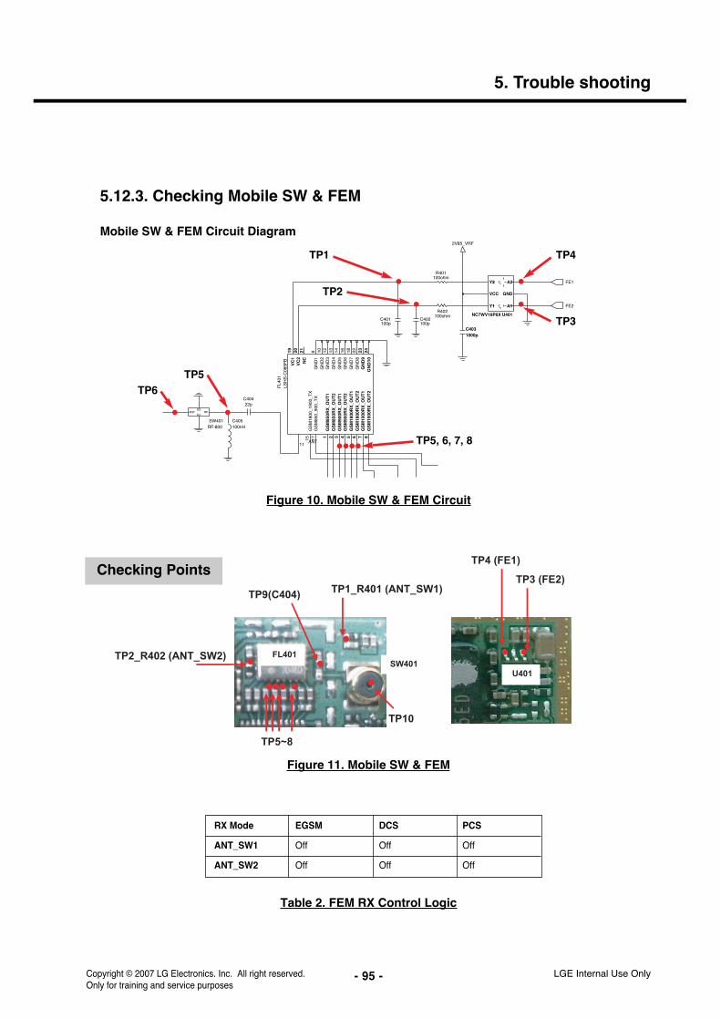
5.12.3. Checking Mobile SW & FEM
Mobile SW & FEM Circuit Diagram
C402100p
2V85_VRF
100pC401
100ohm
A1
A2
GNDVCC
Y1
Y2
R401
NC7WV16P6X U401
22pC404
100nHC405
GS
M85
0RX
_OU
T1
2G
SM
850R
X_O
UT
2
17G
SM
850_
900_
TX
GS
M90
0RX
_OU
T1
3 4G
SM
900R
X_O
UT
2
NC
2119V
C1
VC
220
ANT
GN
D1
9
GN
D10
24
GN
D2
10 12G
ND
3G
ND
413
GN
D5
14
GN
D6
16 18G
ND
722
GN
D8
GN
D9
23
5G
SM
1800
RX
_OU
T1
6G
SM
1800
RX
_OU
T2
15G
SM
1800
_190
0_T
X
GS
M19
00R
X_O
UT
17 8
GS
M19
00R
X_O
UT
2
1
LSH
S-C
085F
BF
L401
11
C4031000p
R402100ohm
RF-800SW401
ANTG1
G2RF
FE2
FE1
Figure 10. Mobile SW & FEM Circuit
TP1 TP4
TP3
TP2
TP6TP5
TP5, 6, 7, 8
LGE Internal Use OnlyCopyright © 2007 LG Electronics. Inc. All right reserved. Only for training and service purposes
5. Trouble shooting
- 95 -
Figure 11. Mobile SW & FEM
SW401TP2_R402 (ANT_SW2) FL401
U401
TP10
TP1_R401 (ANT_SW1) TP3 (FE2)
TP4 (FE1)
TP5~8
TP9(C404)
Table 2. FEM RX Control Logic
Checking Points
RX Mode EGSM DCS PCS
ANT_SW1 Off Off Off
ANT_SW2 Off Off Off

LGE Internal Use Only Copyright © 2007 LG Electronics. Inc. All right reserved. Only for training and service purposes
5. Trouble shooting
- 96 -
Checking Flow
Check TP10 of SW401 with RF Cable and TP9 of C404
TP10 Signal same as TP9?
Replace Mobile SW (SW401)
Yes
No
Yes
Mobile SW & FEM is OK. Check Antenna.
Check NC7WV16P6X (TP3, TP4 for U401) Control Signal is
OK ? No
Yes
Check TP1, TP2 of FL401 ? ?
Replace FEM (U401) TP5~8 Signal is OK ? No
Yes
EGSM RXANT SW1
ANT SW2
Figure 12 Mobile SW Figure 13 FEM Control Signals

LGE Internal Use OnlyCopyright © 2007 LG Electronics. Inc. All right reserved. Only for training and service purposes
5. Trouble shooting
- 97 -
5.12.4. Checking RX I/Q Signals
Checking Flow
17
VDDXO2V815
XO
11 12X
OX
1000pC438
RX
3X
RX
42223
RX
4X
36TX1
37TX2
34VBIAS
VCO_RC18
31V
DD
BIA
S2V
8
8V
DD
DIG
1V5
VD
DD
IG2V
85
21V
DD
LNA
1V5
VDDMIX2V839
VDDRX1V51920
VDDRX2V8VDDTX1V535
38VDDTX2V8 VDDVCO2V8
DA
16EN
FE
132
FE233
14FSYS1
10F
SY
S2
FS
YS
39
13GND1
GN
D2
26
40GND3
GND441
29R
X1
RX
1X30 27
RX
2R
X2X
28
RX
32425
U403PMB6272
A1 2
AX
B3 4
BX
CLK
76
47nC434
820R411
BT_CLK
RF_DA
RF_CLK
QX
Q
IX
I
Check RX I/Q sign als(TP1~TP4)
Signals ar e Normal?
Replac e Transceiver
PMB6272(U403)
Yes
No
RX Part is OK.Check B ase Band Circu it
or Re-Download S/W and Cal
Checking Points
I
I
Q
Q
RX
U403
TP1(I) TP2(IX) TP3(Q)
TP4(QX)
Figure 14. RX I/Q Circuit
Figure 15. RX I/Q
Figure 16. RX I/Q Waveform
TP1(I)
TP2(IX) TP3(Q)
TP4(QX)

LGE Internal Use Only Copyright © 2007 LG Electronics. Inc. All right reserved. Only for training and service purposes
5. Trouble shooting
- 98 -
5.13. Trouble Shooting of Transmitter Part
Checking Flow
Check point VCTCXO
Check point PLL Control
Setup Test Equipment Cell Power : ñ74dBm
EGSM CH30 DCS CH699
Check point TX I/Q Signal
Re-Download S/W & RF CAL
Check point Transceiver
Check point PAM Control
Check FEM & Mobile
SW
Checking Points
Figure 17. Main PCB
Figure 18. Main PCB Bottom

LGE Internal Use OnlyCopyright © 2007 LG Electronics. Inc. All right reserved. Only for training and service purposes
5. Trouble shooting
- 99 -
5.13.1. Checking VCTCXO CircuitSee RX Part “1. Checking VCTCXO Circuit”
5.13.2. Checking PLL Control SignalSee RX Part “2. Checking PLL Control Signal”
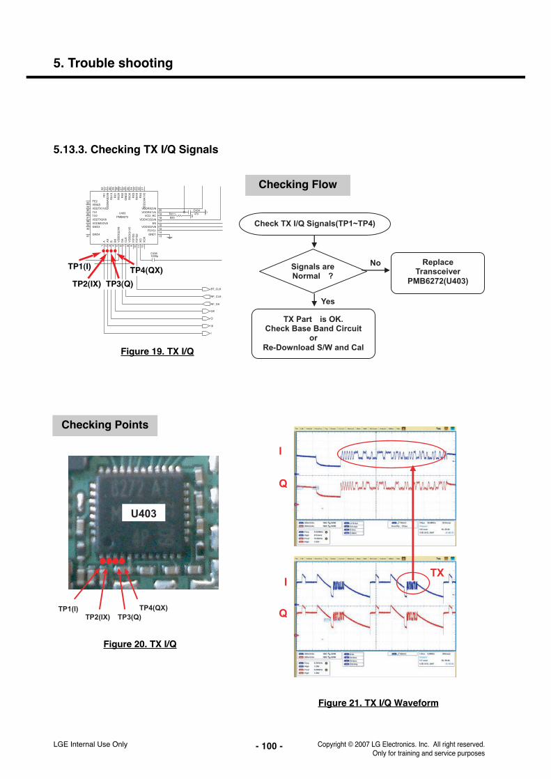
LGE Internal Use Only Copyright © 2007 LG Electronics. Inc. All right reserved. Only for training and service purposes
5. Trouble shooting
- 100 -
5.13.3. Checking TX I/Q Signals
Checking Flow
Check TX I/Q Signals(TP1~TP4)
Signals are Normal ?
Replace Transceiver
PMB6272(U403)
Yes
No
TX Part is OK. Check Base Band Circuit
or Re-Download S/W and Cal Figure 19. TX I/Q
17
VDDXO2V815
XO
11 12X
OX
1000pC438
RX
3X
RX
42223
RX
4X
36TX1
37TX2
34VBIAS
VCO_RC18
31V
DD
BIA
S2V
8
8V
DD
DIG
1V5
VD
DD
IG2V
85
21V
DD
LNA
1V5
VDDMIX2V839
VDDRX1V51920
VDDRX2V8VDDTX1V535
38VDDTX2V8 VDDVCO2V8
DA
16EN
FE
132
FE233
14FSYS1
10F
SY
S2
FS
YS
39
13GND1
GN
D2
26
40GND3
GND441
29R
X1
RX
1X30 27
RX
2R
X2X
28
RX
32425
U403PMB6272
A1 2
AX
B3 4
BX
CLK
76
47nC434
820R411
BT_CLK
RF_DA
RF_CLK
QX
Q
IX
I
TP1(I)
TP2(IX) TP3(Q)
TP4(QX)
Checking Points
I
Q
I
Q
TX
U403
TP1(I) TP2(IX) TP3(Q)
TP4(QX)
Figure 20. TX I/Q
Figure 21. TX I/Q Waveform

LGE Internal Use OnlyCopyright © 2007 LG Electronics. Inc. All right reserved. Only for training and service purposes
5. Trouble shooting
- 101 -
5.13.4. Checking Transceiver Output Signals
Checking Points
1V5_VRF
17
VDDXO2V815
XO
11 12X
OX
1000pC438
RX
3X
RX
42223
RX
4X
36TX1
37TX2
34VBIAS
VCO_RC18
31V
DD
BIA
S2V
8
8V
DD
DIG
1V5
VD
DD
IG2V
85
21V
DD
LNA
1V5
VDDMIX2V839
VDDRX1V51920
VDDRX2V8VDDTX1V535
38VDDTX2V8 VDDVCO2V8
DA
16EN
FE
132
FE233
14FSYS1
10F
SY
S2
FS
YS
39
13GND1
GN
D2
26
40GND3
GND441
29R
X1
RX
1X30 27
RX
2R
X2X
28
RX
32425
U403PMB6272
A1 2
AX
B3 4
BX
CLK
762V85_VRF
10R412
0.22uC443
820R411
10
R418
C4300.1u
1V5_VRF
0.1uC444
C4360.22u
LBAND_PAM_INHBAND_PAM_IN
BT_CLK
TP1(LBNAD_PAM_IN)
TP2(HBNAD_PAM_IN)
MODE Transceiver Output
GMSK Fixed
8PSK Ramp Burst Control
Figure 22. Transceiver Output Circuit
Figure 23. Transceiver Output
Table 3. Transceiver Output Operation
TP1(LBNAD_PAM_IN)
TP2(HBNAD_PAM_IN)

LGE Internal Use Only Copyright © 2007 LG Electronics. Inc. All right reserved. Only for training and service purposes
5. Trouble shooting
- 102 -
Checking Flow
LBAND_PAM_IN (MODE: GMSK): TP1 LBAND_PAM_IN (MODE: 8PSK): TP1
Signals are Normal ?
Replace PMB6272(U403)
Yes
No
Transceiver is OK. See next page to check
PAM Control Circuit.
Check Output Signal(TP1, TP2)
Figure 24. Transceiver Output (GMSK) Figure 25. Transceiver Output (8PSK)

LGE Internal Use OnlyCopyright © 2007 LG Electronics. Inc. All right reserved. Only for training and service purposes
5. Trouble shooting
- 103 -
5.13.5. Checking PAM Control Signals
820pC429
100pC413
1.2KR409
C428100p100p
C427
PA_LEVELLBAND_PAM_IN
HBAND_PAM_IN
TXON_PA
PA_MODE
PA_BAND
Checking Points
U403
TP3(PA MODE)
TP2(TXON PA)
TP1(PA LEVEL)
MODE MODE PA_LEVEL TXON_PA
GMSK LOW Ramp Burst Control HIGH
8PSK HIGH Control Amp bias HIGH
Figure 26. PAM Control Signals
Figure 27. Transceiver Output
Table 4. PAM Mode Operation
TP2(TXON PA)
TP1(PA LEVEL)TP3(PA MODE)

LGE Internal Use Only Copyright © 2007 LG Electronics. Inc. All right reserved. Only for training and service purposes
5. Trouble shooting
- 104 -
Checking Flow
Signals are Normal ?
Check PMB8877(U102)
Yes
No
PAM Control Signal is OK.
See next page to check FEM & Mobile SW Circuit.
Check Control Signals(TP1, TP2, TP3)
TP3(PA MODE) : C427 TP1(PA_LEVEL) : R409 TP2(TXON_PA) : R428
TP1(PA LEVEL)
TP2(TXON PA)
TP3(PA MODE)
TP1(PA LEVEL)
TP2(TXON PA)
TP3(PA MODE)
TP1(PA LEVEL)
TP2(TXON PA)
TP3(PA MODE)
Figure 28. GSMK Control Signal Figure 29. 8PSK Control Signal
TP3(PA MODE): C427TP1(PA_LEVEL): R409TP2(TXON_PA): R428

LGE Internal Use OnlyCopyright © 2007 LG Electronics. Inc. All right reserved. Only for training and service purposes
5. Trouble shooting
- 105 -
5.13.6. Checking FEM & Mobile SW
Mobile SW & FEM Circuit Diagram
C402100p
2V85_VRF
100pC401
100ohm
A1
A2
GNDVCC
Y1
Y2
R401
NC7WV16P6X U401
22pC404
100nHC405
GS
M85
0RX
_OU
T1
2G
SM
850R
X_O
UT
2
17G
SM
850_
900_
TX
GS
M90
0RX
_OU
T1
3 4G
SM
900R
X_O
UT
2
NC
2119V
C1
VC
220
ANT
GN
D1
9
GN
D10
24
GN
D2
10 12G
ND
3G
ND
413
GN
D5
14
GN
D6
16 18G
ND
722
GN
D8
GN
D9
23
5G
SM
1800
RX
_OU
T1
6G
SM
1800
RX
_OU
T2
15G
SM
1800
_190
0_T
X
GS
M19
00R
X_O
UT
17 8
GS
M19
00R
X_O
UT
2
1
LSH
S-C
085F
BF
L401
11
C4031000p
R402100ohm
RF-800SW401
ANTG1
G2RF
FE2
FE1
Checking Points
SW401TP2_R402 (ANT_SW2) FL401
U401
TP4 (FE1) TP3 (FE2) TP1_R401 (ANT_SW1)
TP5(C404) TP6
Figure 30. Mobile SW & FEM Circuit
Figure 31 Mobile SW & FEM
Table 5. FEM TX Control Logic
RX Mode GSM850 DCS PCS
ANT_SW1 On Off Off
ANT_SW2 Off On On
TP1 TP4
TP3
TP2
TP6TP5
TP5, 6, 7, 8

LGE Internal Use Only Copyright © 2007 LG Electronics. Inc. All right reserved. Only for training and service purposes
5. Trouble shooting
- 106 -
Checking Flow
Check TP6 of SW401 with RF Cable and TP5 of C404
TP6 Signal same as TP6?
Replace Mobile SW (SW401)
Yes
No
Yes
Mobile SW & FEM is OK.Check Antenna.
Check NC7WV16P6X
(TP3, TP4 for U401) Contro l Signal is OK ? No
Yes
Check TP1, TP2 of FL401 ? ?
Replace FEM (U401) TP5 Sign al is OK ? No
Yes
?
EGSM TX
TP1(ANT SW1)
TP2(ANT SW2)
Figure 32 Mobile SW Figure 33 FEM Control Signals

LGE Internal Use OnlyCopyright © 2007 LG Electronics. Inc. All right reserved. Only for training and service purposes
6. Download & S/W upgrade
- 107 -
6. Download & S/W upgrade
6.1. S/W download setup
Preparation• Target terminal• PIF-Union• RS-232 Cable and PIF-UNION to Phone interface Cable• Power Supply or Battery• PC supporting RS-232 with Windows 2000 or newer.
If you are going to use battery, the voltage of the battery should be over 3.7V for stable powersupplying during S/W download.
Figure S/W download & upgrade setup

LGE Internal Use Only Copyright © 2007 LG Electronics. Inc. All right reserved. Only for training and service purposes
6.2. Download program user guide
6. Download & S/W upgrade
- 108 -
Uncheck this
1. Double Click “Flash tool E2.exe”
2. Click

LGE Internal Use OnlyCopyright © 2007 LG Electronics. Inc. All right reserved. Only for training and service purposes
6. Download & S/W upgrade
- 109 -
Check this
3. Select Download Files.
4. Press the “ START” button

- 110 -
6. Download & S/W upgrade
LGE Internal Use Only Copyright © 2007 LG Electronics. Inc. All right reserved. Only for training and service purposes
5. Click “Start USB1” connect the Phone
Downloading: END

- 111 -
PWRURXDUTXD
3G 2.5G
GNDRXTXVCHARON_SWVBAT
BASE BAND PROCESSOR
63
B
126
E
D
9
2
7
1
H
F
2 3
C
4
8
9
C
5
117
A
10
F
UART
ON BOARD ARM9 JTAG & ETM INTERFACE
A
11
E
G
1
H
1G NAND +512M DDR SDRAM
B
8
G
4
D
5 1210
C11
0
TP101
0.1u
27pC137
680
R11
4
X101
32.768KHz12
2V5_VAUDA
1000
pC
136
C130
2V62_VIO
2V5_VAUDB
0.1u
TP102
TP104K
8
VS
S_M
AIN
6M
11M
10V
SS
_MA
IN7
M9
VS
S_M
AIN
8V
SS
_MA
IN9
M8
VS
S_P
LLT
12
VS
S_R
TC
AA
14
VS
SA
_M
VS
SA
_VB
R1
R17
VS
SA
_VB
R2
U17
VS
SA
_VB
TN
17
VS
SP
_DIG
1H
2A
7V
SS
P_D
IG2
J17
VS
SP
_DIG
3
VS
SP
_DIG
4B
10
U1
VS
SP
_ME
M_E
TM
1V
SS
P_M
EM
_ET
M2
V2
VS
SP
_ME
M_E
TM
3W
1W
10V
SS
P_M
EM
_ET
M4
VS
S_M
AIN
1K
12
VS
S_M
AIN
2K
11K
10V
SS
_MA
IN3
K9
VS
S_M
AIN
4V
SS
_MA
IN5
J9 L12
VD
D_M
AIN
4L1
1V
DD
_MA
IN5
VD
D_M
AIN
6L1
0L9
VD
D_M
AIN
7V
DD
_MA
IN8
L8
VD
D_M
AIN
9N
10
VD
D_P
LLW
13
AA
13V
DD
_RT
C
U16
VM
ICN
VM
ICP
T15
P16
VR
EF
NR16
VREFP
VS
SA
_BB
L15
VS
SA
_BG
U14
T14
VS
SA
_D
W15
A5
A16
VD
DP
_DIG
C1
C17
VD
DP
_DIG
C2
VD
DP
_DIG
DB
2
H1
VD
DP
_DIG
E
AA
10V
DD
P_M
EM
_ET
M1
AA
3V
DD
P_M
EM
_ET
M2
VD
DP
_ME
M_E
TM
3A
A6
VD
DP
_ME
M_E
TM
4Y
1P
1V
DD
P_M
EM
_ET
M5
VD
DP
_MM
CA
13K
19V
DD
P_S
IM
L2V
DD
_FU
SE
_FS
J11
VD
D_M
AIN
1
N9
VD
D_M
AIN
10
VD
D_M
AIN
2J1
0
VD
D_M
AIN
3
F3
US
IF2_
CT
S_N
F14
G16
US
IF2_
RT
S_N
US
IF2_
RX
D_M
RS
TH
19 J16
US
IF2_
TX
D_M
TS
R
US
IF3_
RX
D_M
RS
TE
3
US
IF3_
SC
LKE
4E
2U
SIF
3_T
XD
_MT
SR
P15
VD
DA
_BB
T13
VD
DA
_BG
VD
DA
_DT
16
VD
DA
_MU
13
VD
DA
_VB
R1
T17
VD
DA
_VB
R2
W19
N18
VD
DA
_VB
T
VD
DP
_DIG
AF
17
VD
DP
_DIG
B
T_IN0T_IN1
C13
T_OUT0E13B14
T_OUT1
B12T_OUT10
T_OUT2F11A15
T_OUT3T_OUT4
E11F12
T_OUT5T_OUT6
B13
T_OUT7C11E12
T_OUT8T_OUT9
C12
F4
US
IF1_
CT
S_N
E1
US
IF1_
RT
S_N
US
IF1_
RX
D_M
RS
TF
5
US
IF1_
TX
D_M
TS
R
TCK
TDIB18A18
TDO
C15TMS
TRACECLKU11
AA
8T
RA
CE
PK
T0
TR
AC
EP
KT
1Y
10A
A12
TR
AC
EP
KT
2T
RA
CE
PK
T3
AA
11A
A9
TR
AC
EP
KT
4T
RA
CE
PK
T5
Y15
Y11
TR
AC
EP
KT
6T
RA
CE
PK
T7
Y12
AA7TRACESYNC
TRIG_INE14
TRST_NF13
B15
T10PIPESTAT2
Y9
PM
_IN
TY
13
RESET_NW14
B17RF_CLK
E15RF_DATA
D17RF_STR0RF_STR1
D18
H18RSTOUT_N
F16RTCK
Y14RTC_OUT
H17SPCU_RC_OUT0
J18SPCU_RQ_IN0SPCU_RQ_IN1
J19
SPCU_RQ_IN2G18
H15SWIF_TXRX
C16
M_0M_1
V17
U15M_10
Y19M_2M_3
Y18W17
M_4M_5
AA18Y17
M_6M_7
W16AA17
M_8M_9
Y16
NC
N11
AA15OSC32K
PAOUT11K16M12
PAOUT12
Y8PIPESTAT0PIPESTAT1
MEM_WRNM
ICN
1N
19
M18
MIC
N2
P19
MIC
P1
MIC
P2
M17
A12MMCI1_CLK
E10MMCI1_CMD
MMCI1_DAT0B11C9
MMCI1_DAT1MMCI1_DAT2
F10A14
MMCI1_DAT3
F6MMCI2_CLK
MMCI2_CMDD3
MMCI2_DAT0D2
B16MON1MON2
C10
W18
W3Y3
MEM_BFCLKO2
W8MEM_CAS_N
MEM_CKEU10
MEM_CS0_NR2P3
MEM_CS1_NMEM_CS2_N
N3
MEM_CS3_NN4U3
MEM_CSA0_NMEM_CSA1_N
U4T6
MEM_CSA2_NT5
MEM_CSA3_N
MEM_RAS_NY7
MEM_RDNL1
MEM_SDCLKOY2
MEM_WAITNK2
R3
MEM_AD13MEM_AD14
M4P4
MEM_AD15
J3MEM_AD2MEM_AD3
L5M3
MEM_AD4MEM_AD5
N1P2
MEM_AD6MEM_AD7
N2J4
MEM_AD8K4
MEM_AD9
M1MEM_ADVN
AA2MEM_BC0_N
V3MEM_BC1_NMEM_BC2_N
U5Y4
MEM_BC3_N
MEM_BFCLKO1
T2
MEM_A24P5T3
MEM_A25T4
MEM_A26
MEM_A3U6
MEM_A4W5AA4
MEM_A5MEM_A6
T7U7
MEM_A7MEM_A8
Y5AA5
MEM_A9
M2MEM_AD0MEM_AD1
L3
MEM_AD10K5L4
MEM_AD11MEM_AD12
R1M5
MEM_A0MEM_A1
W4
MEM_A10W6T9
MEM_A11MEM_A12
W7Y6
MEM_A13U9
MEM_A14MEM_A15
W9V1
MEM_A16MEM_A17
N5U2
MEM_A18MEM_A19
W2
T8MEM_A2
R5MEM_A20MEM_A21
T1R4
MEM_A22MEM_A23
F19
G17
I2S
2_W
A1
G2IRDA_RXIRDA_TX
F2
IREFR15
KP
_IN
0G
1
KP
_IN
1J5 H3
KP
_IN
2H
5K
P_I
N3
KP
_IN
4J2
KP
_IN
5J1 K3
KP
_IN
6G
4K
P_O
UT
0K
P_O
UT
1G
3
KP
_OU
T2
F1
G5
KP
_OU
T3
U8
FCDP_RBN
FWPW11
J15
GU
AR
D
C14
I2C
1_S
CL
A17
I2C
1_S
DA
I2C
2_S
CL
C19
F15
I2C
2_S
DA
E16
I2S
1_C
LK0
I2S
1_C
LK1
D19
I2S
1_R
XE
18E
17I2
S1_
TX
B19
I2S
1_W
A0
I2S
2_C
LK0
G19
I2S
2_C
LK1
G15
F18
I2S
2_R
XE
19I2
S2_
TX
I2S
2_W
A0
DIF
_WR
H4
DS
PIN
0K
1D
SP
IN1
DS
PO
UT
1E
6
P17
EP
N11
EP
N12
P18
EP
P11
R18
R19
EP
P12
EP
PA
11T
18T
19E
PP
A12
V18
EP
PA
21E
PP
A22
V19
U18
EP
RE
F1
EP
RE
F2
U19
U12F26M
F32KAA16
T11
C1
E5
DIF
_CS
2
DIF
_D0
F7
C6
DIF
_D1
B5
DIF
_D2
DIF
_D3
E7
DIF
_D4
A3
A2
DIF
_D5
B3
DIF
_D6
DIF
_D7
B4
C2
DIF
_D8
DIF
_HD
C4
DIF
_RD
B1
F8
DIF
_RE
SE
T1
DIF
_RE
SE
T2
C7
D1
DIF
_VD
C3
CIF
_D4
B9
CIF
_D5
CIF
_D6
A8
CIF
_D7
E8
E9
CIF
_HS
YN
C
B7
CIF
_PC
LK
A6
CIF
_PD
A10
CIF
_RE
SE
T
CIF
_VS
YN
CA
4
CLKOUT0W12
CLK
OU
T2
B6
A1
CO
RN
ER
_A1
CO
RN
ER
_A2
A19
CO
RN
ER
_AA
1A
A1
AA
19C
OR
NE
R_A
A2
DIF
_CD
C5
DIF
_CS
1
L16
AU
XN
1L1
7
L19
AU
XN
2
M19
AU
XP
1
AU
XP
2L1
8
BB_IN15M15
BB_IXM16
BB_QK15
BB_QX
CC_CLKK18H16
CC_IO
K17CC_RST
F9
CIF
_D0
A11
CIF
_D1
CIF
_D2
A9
CIF
_D3
C8
B8
1V8_SD
PMB8877U102
AFCC18
AG
ND
N16
AU
XG
ND
0.1u
C12
6
0R
127
R12
58.
2K
G4
E9_CS
E7_RAS
E5_RE
D6_WE
_WEDF8
F5_WP
M2
VDDQ1D2
VDDQ2F2
VDDQ3K2
C2VSS1
F9VSS2VSS3
G2N4
VSS4
VSS5B5
VSS6N5N8
VSS7
VSSQ1E2
VSSQ2J2
VSSQ3L2
F7_CAS
_CEC6
_CK
B9
NC
4E
8
NC
5F
6
G5
NC
6G
6N
C7
H5
NC
8N
C9
H6
R__BE6
H3UDQM
J3UDQS
B6VCC1VCC2
N7
N6VCCQ
B4VDD1
G9VDD2VDD3
H2
VDD4
J8
IO7L8
G3LDQM
F3LDQS
NC
1B
2
K5
NC
10N
C11
K6
K7
NC
12N
C13
K8
M5
NC
14N
C15
M6
M7
NC
16N
C17
M8
N2
NC
18N
C19
N9
NC
2B
7
NC
3
M4
DQ15N3
C3DQ2DQ3
D4
DQ4D3
DQ5E4E3
DQ6DQ7
F4
DQ8J4K3
DQ9
J5IO0
L5IO1IO2
J6
IO3L6J7
IO4L7
IO5IO6
P9
P10
DN
U11
DN
U2
A9
A10
DN
U3
B1
DN
U4
B10
DN
U5
DN
U6
N1
N10
DN
U7
DN
U8
P1
P2
DN
U9
DQ0B3
DQ1C4
DQ10K4L3
DQ11DQ12
L4M3
DQ13DQ14
A12
C9A2
B8A3
M9A4A5
L9K9
A6J9
A7H7
A8A9
H8
D5ALE
D7BA0BA1
D8
CKEG8
C5CLE
CLKH4
A2
DN
U1
DN
U10
U101
K5E1G12ACA-D075
C7A0A1
C8
D9A10
H9A11
G7
27pC140
VSUPPLY
24
G1 G2
G3 G4
0.1u
C11
4
9
16
252627282930
17181920212223
1
101112131415
2345678
R11
8
CN101
680
PM
_IN
T
680
R11
5
0.1u
C11
7
R11
3
10K
0.1u
C12
8
C12
1
1V35_CORE
1u
C11
80.
1u
2V11_RTC
1V8_SD
C10
50.
1uTP103
2V9_SIM
1uC
124
1uC
101
8.2K
R12
4
C10
80.
1uC
107
TP
111
1u
1KR
110
2V8_VMME
0.1u
C11
1
390K
R10
2
R11
2
22K
0R
126
VBAT
1V8_SD
0.1u
C10
9
CTS12
DSR10
GND1
NC14
7NC2
NC389
NC4
5ON_SW
11RTS
RX23
TX
6
UT101
C12
00.
1u
R10
5
10K
1uC
104
R103
NA
C10
60.
01u
TP
110
TP107
R108 0
C10
20.
1u
OJ102
TP105
C12
70.
1u
1V8_SD
3.3K
R10
6
C11
90.
1u
680
R12
1R
122
680
27pC139
0.1u
C11
6
0.1u
C12
9
C1320.1u0.1u
C131
1V8_SD
TP108
C13515p
0.1u
1V8_SD
C12
2
C10
30.
01u
C133
OJ101
220n
C12
50.
1u
C11
5
TP
109
100K
R10
4
0.1u
C134
1V8_SD
2V62_VIO
15p
0.1u
C11
3
R11
1
10K
2V62_VIO
1V35_VPLL
R10
10
R11
768
068
0R
116
R12
068
0
C11
20.
1u
C13827p
R11
968
0
0.1u
TP106
C12
3
R12
30
CAM_LDO_EN
ICDL
2V62_VIO
DS
R
VS
YN
C
VIB_EN
JACK_TYPEREMOTE_ADC
TRIG_IN
SIM_DETECT
_AMP_SHDNMAIN_BACKLIGHT
SIM_CLK
SP
K_E
N
VIB_PWM
UA
RT
_BT
_RX
DATA(0:15)
CA
ME
RA
_ST
B
FE1
US
B_D
AT
_VP
US
B_S
E0_
VM
TS
_IR
Q
MM
C_D
ET
EC
T
KE
Y_E
N
BT
_IN
T
RPWRON
_CHG_EN
ISP_LDO_EN
ADD(23)ADD(24)ADD(25)
ADD(16:28)
SUB_BACKLIGHT
ISP
_RE
SE
T
FM
_SN
D_L
FM
_SN
D_R
EA
R_N
EA
R_P
FE2
UA
RT
_BT
_TX
ADD(16)ADD(17)
ADD(26)ADD(27)ADD(28)
ADD(18)ADD(19)ADD(20)ADD(21)ADD(22)
DATA(0)DATA(1)DATA(2)DATA(3)DATA(4)DATA(5)DATA(6)DATA(7)
ADD(0:15)
DATA(0:7)
SDCLKO
_WR
_BC0_BC1
_NAND_CS
ADD(16)ADD(17)
_RD
_WRFCDP
ADD(9)ADD(10)ADD(11)ADD(12)ADD(13)ADD(14)ADD(15)
_RAM_CS
ADD(29)ADD(30)
CKE
_CAS_RAS
UDQS
SDCLKI
ADD(0)ADD(1)ADD(2)ADD(3)ADD(4)ADD(5)ADD(6)ADD(7)ADD(8)
PA_LEVEL
LDQS
TRACEPKT5TRACEPKT6TRACEPKT7TRACECLK
PIPESTAT0PIPESTAT1PIPESTAT2
TRACESYNC
DIF
_SU
B_C
S
ADD(0:26)
ADD(26)
ADD(27)ADD(28)ADD(29)ADD(30)
LDQSUDQS
TRSTnTDI
TMSTCK
RTCKTDO
EXTRSTnTRIG_IN
TRACEPKT0TRACEPKT1TRACEPKT2TRACEPKT3TRACEPKT4
ISP
_MC
LK
UA
RT
_BT
_CT
SU
AR
T_B
T_R
TS
I2C
2_C
LK1
I2C
2_D
AT
A1
BB
_SN
D_R
KP
_OU
T(0
)
KP
_OU
T(3
)
DIF
_D(8
)
WD
OG
SLI
DE
_DE
TE
CT
SDCLKI
MMC_CLKMMC_CMD
MMC_D(0)
MMC_D(3)
KP
_IN
(0)
KP
_OU
T(2
)
RE
MO
TE
_IN
T
LCD
_ID
KP
_OU
T(1
)
KP
_IN
(1)
KP
_IN
(2)
KP
_IN
(3)
KP
_IN
(4)
CLK
32K
_PP
R
ISP
_HS
ISP
_PC
LK
ISP
_VS
USB_OEn
VREFN
SDCLKO
AFC
PA_BAND
PA_MODE
JACK_DETECT
UA
RT
_RX
MMC_D(2)MMC_D(1)
VC
XO
_EN
VM
IC_N
VM
IC_P
VR
EF
N
RF_CLKRF_DA
RF_EN
RTCKRTC_OUT
I2C
1_C
LKI2
C1_
DA
TA
TCK
TDITDO
TMS
TRACECLK
TR
AC
EP
KT
0T
RA
CE
PK
T1
TR
AC
EP
KT
2T
RA
CE
PK
T3
TR
AC
EP
KT
4T
RA
CE
PK
T5
TR
AC
EP
KT
6T
RA
CE
PK
T7
TRACESYNC
TRSTn
TXON_PA
I2S
1_W
A0
EO
C
BAT_IDRF_TEMP
MA
IN_M
IC_N
HS
_MIC
_N
MA
IN_M
IC_P
HS
_MIC
_P
LOAD
PIPESTAT0PIPESTAT1PIPESTAT2
PM
_IN
T
_RESET
_NAND_CS
_BC0_BC1
FCDP
_CASCKE
_RAM_CS
_RD_WR
BB
_SN
D_L
26MHZ_MCLK
I2S
1_C
LK
I2S
1_R
XI2
S1_
TX
ADD(16)
ADD(17)
ADD(18)
ADD(19)
ADD(2)
ADD(20)
ADD(21)
ADD(22)
ADD(23)
ADD(24)
ADD(3)
ADD(4)
DATA(0)
DATA(1)
DATA(3)
DATA(4)
DATA(5)
DATA(6)
DATA(7)
DATA(2)
ADD(25)
DIF
_D(2
)D
IF_D
(3)
DIF
_D(4
)D
IF_D
(5)
DIF
_D(6
)D
IF_D
(7)
DIF
_RE
SE
T
DIF
_WR
UA
RT
_TX
ADD(0)
ADD(1)
ADD(10)
ADD(5)
ADD(11)
ADD(6)
ADD(12)
ADD(7)
ADD(13)
ADD(8)
ADD(14)
ADD(9)
ADD(15)
QX
SIM_IO
SIM_RST
ISP
_DA
TA
(0)
ISP
_DA
TA
(1)
ISP
_DA
TA
(2)
ISP
_DA
TA
(3)
ISP
_DA
TA
(4)
ISP
_DA
TA
(5)
ISP
_DA
TA
(6)
ISP
_DA
TA
(7)
HO
OK
_DE
TE
CT
DIF
_CD
DIF
_MA
IN_C
S
DIF
_D(0
)D
IF_D
(1)
UART_CTS
RPWRON_EN
UART_RX
UART_RTSDSR
UART_TX
VSUPPLY
RE
SO
UR
CE
_CT
RL
BT
_RE
SE
Tn
_RAS
IIXQ
7. CIRCUIT DIAGRAM
LGE Internal Use OnlyCopyright © 2007 LG Electronics. Inc. All right reserved. Only for training and service purposes

- 112 -
GND
IN
OUT
D
7
H
EXTERNAL RESET
10
A
LOW
8
3
3
11
MAIN BACKLIGHT
7
E
52
SUB BACKLIGHT
C
SPK_EN
G
6
Remote Power On
-
C
H
F
Flash LED
11
PMIC
1
4
RCV
12
109
B B
A
4 6
D
2
+
HIGH
MODE
VIBRATOR
Battery Connector & Current Monitor
F
CHARGING IC E
SPK
SIM & MMC Connetor
1 9
12
5 8
G
HP AMP & SPK
1KR24
2
2.2uC259
5.1K
R24
0
10pC264
11D2
12D3D4
1
2EN_SET
GND9
PGND13
8VIN
VOUT5
2V62_VIO
AAT3151IWP_T1U206
C1+3
4C1-
6C2+
C2-710
D1
SW201SPVM110200
1 2
3 4
1
2
2.2u
C22
7
CN201
0.1uC236
R24
8
280K
ohm
VBAT
NAC257
C23
210
u
R227 0
2.2uC260
22K
TP202
R205
NAR202
0.1u
C21
2
C27
9
2.2u
522B0
32B1
4GND
S17
S26
9VCC
C2400.1u
U202 FSA2268TUMX8
1A1B010
1B11
2A
47pC262
ZXCT1010E5TA
U204
2GNDIOUT
3
5LOAD NC
1
4VIN
1uC268
100K
R21
6
4.7K
R20
7
C2472.2u
C2282.2u
L202100nH
C253NA
C21
31u
47mohmR226
R2302200
C230
2V85_AMP
1u
A2 3
B16
B2 2
GND4
VCC 8
Y1 1
Y25
820k
R24
9
U208NC7WZ08L8X
A17
10uHL201
USB_VBUS
1V8_EXT
2V9_SIM
R24662K
R250 120K
22u
51KR245
1V35_CORE
C237
0R213
10KR244
L203100nH
3VOUT
R1114D311DU207
CE6
2GND1
5GND2
4NC
VDD1
47pC223
2.2uC221
C21
12.
2u
R20
40
R241100K
C286
R21
4
1u
4.7K
100K
R22
0
C1N
C4
C1P
A4
C1INL
A1INR
B3
NC
1C
3N
C2
OUTLD2
OUTRC2
PGNDB4
A3PVDD PVSS
D4
SGNDA2
D1SVDD
D3SVSS
_SDLB2B1
_SDR
12 3 4 5
U201 TPA4411YZH
2V11_RTC
LMFL4PA1WHZ180LD201
EX
T_O
N
2V5_VAUDB
1000pC261
2V9_SIM2V11_RTC
R251 0
R21
14.
7K
C21
5
VBAT
0.1u
C2832.2u
R20
9N
A2.2uC241
C27
41u
1uC245
C2872.2u
VA
202
ICV
L051
8400
V50
0FR
2V5_VAUDA
R21
21u
100K
C28
0
R21
5
100K
R231
39K
22KR203
100u
PMRSTn
VBAT
C206
C2392.2u
7FBB
24FENS
FL12322
FL2FL3
21
FL420
FSET3
9IN1IN2
18
14OUT
11OUTA
8OUTB
19P
GN
D
6REF
AG
ND
4
BENS25
BL1128
BL2BL3
2726
BL4
2BSET
C1+
13 12C
1-
16C
2+ C2-
17
5CT
ENL15
EP
29
FBA10
1u
AAT2842IBJ-EE-T1U210
C265
100pC225
C2691u
0.1u
C28
5
100nH
L205
VBAT
2V62_VIO
10BAT
1CRDL
GND8
9ICDL
IMIN6
11PGND
USB2
7USBON
_CHG4
5_EN
3_PPR
Q203
KRC402E
B
C
E
U205 ISL6299
51KR243
2V62_VIO
2.2uC248
2.2u1uC249C243
FB
201
R23
9
100K
VBAT
2V85_AMP
100K
R21
9
2.2uC246C242
2.2u
4.7K
R20
8
TPA6205A1ZQVRU209
BYPASSC1
GNDB2
C2IN+
C3IN-
A3VDD
VO+B3
VO-A1B1
_SHUTDOWN
VBAT
47
R221
G1
G2
1
2
3
CN202
1u
C21
02.
2u
C254
1V8_SD
R21
04.
7K
U_VMIN
C2820.1u
10u
C23
1
KD
S16
0E
VBAT
2V85_VRF
D20
2
C2711u
C266100p
0.1uC201
C276
C20
52.
2u
0.01u
4.7K
C251
R20
6
2V8_VMME
2.2u
C220 2.2u
VBAT
C2192.2u
VBAT
VCHG_VUSB
R253 100K
2.2u
C203
1uFC252
C23510u
27pC263
27pC222
100nHL207
L208100nH
45
T4T5
67
T6T7
8
T89
100K
R22
3
19G
1G
220
G3
21
S1
16
S2
1412S
3
S41
15S
5
13S
6
S7
11
10S8
17ST1ST2
18
2T1
3T2T3
VBAT
S20
1
ICV
L051
8400
V50
0FR
VA
201
R232
160K
0.1uC258
VCHG_VUSB
D20
1
KD
S16
0E
4.7uC278
C21668p
C207 1u
0.1u
C284
2.2uC202
R222
100K
SP
_IN
T
U_RCV
C244
1uC272
1u
C2771u
VBAT
2.2uC250
2V8_VLCD
R238 110K
R22
4
100K
1V8_SD
2.2u
C20
4
VVIBF11
WD
OG
L310u
C234 H6
VS
S28
VS
S29
H7
D5
VS
S3
J6V
SS
30
VS
S4
D6
D7
VS
S5
VS
S6
D8
E4
VS
S7
VS
S8
E5
E6
VS
S9
C7
VS
S_M
ON
O
VS
S_S
D1
H8
H4
VS
S_S
D2
D9
VS
S_V
RE
F
J11VUMTS
A4
VU
SB
F3
VS
S13
VS
S14
F4
F5
VS
S15
VS
S16
F6
F7
VS
S17
VS
S18
F8
F9
VS
S19
VS
S2
D4
VS
S20
G3
G4
VS
S21
VS
S22
G5
VS
S23
G6
G7
VS
S24
VS
S25
G8
G9
VS
S26
VS
S27
H5
C11VMME
C2VPIN
VP
LLA
10
VR
EF
C8
VR
EF
EX
_MA
5
F10VRF1
VRF2D11
E10VRF3
VRTCH10
VS
D1
L11
VS
D2
L1
VSIMG10
C6
VS
S1
VS
S10
E7
E8
VS
S11
VS
S12
E9
VDDAUXH1
VDDMMEC10
B9
VD
DP
LLIO
VDDRF13_AFCE11
D10VDDRF2
VDDSD1K11
VDDSD2K1
G11VDDSIMVIB
VDDUMTSH9
K9
VD
D_C
HA
RG
E
B7
VD
D_M
ON
O
VD
D_R
EF
J9B5
VD
D_U
SB
A11
VIO
A8
VLE
D
VMIND3
SE
NS
E_I
N1
L9 K10
SE
NS
E_I
N2
E2SLEEP1_NSLEEP2_N
E1
H3SU1_FB
J1SU1_GATESU1_GND
J2
SU1_ISENSEJ3
A3
SU
SP
EN
D
TX
ON
PA
B10
H11VAFC
F2VAUDIOA
VAUDIOBG1
H2VAUX
VDDAUDIOAF1
G2VDDAUDIOB
L5O
N_O
FF
_OU
T
OU
TP
OR
TJ4 K
3P
OW
ER
_ON
A1
PU
MS
1P
UM
S2
B4
B11
PU
MS
3
RCVB1
RESET2_ND1E3
RESET_N
RE
SO
UR
CE
_CR
TL
J5B8
RR
EF
J10SD1_FB
SD1_FBLL10K2
SD2_FBSD2_FBL
L2
B2
SE
0_V
M
K8
CH
_SO
UR
CE
C1D+D-
D2
DA
T_V
PA
2
C9
FLA
SH
_ON
FLA
SH
_SH
INK
A9
J7I2
C_C
LKI2
C_D
AT
K6
K5
I2C
_IN
T
MO
NO
_IN
NC
5M
ON
O_I
NP
B6
MO
NO
_OU
TN
A6
MO
NO
_OU
TP
A7
OE
_NC
4
K4
ON
_OF
F1
ON
_OF
F2
L4
PMB6821U203
B3
AC
+A
C-
C3
L6B
L1_P
WM
BL2
_PW
MK
7J8
BL3
_PW
M
CH
AR
GE
_UC
L8
CH
_CN
TR
LL7
TP201
1uC
273
FB202
C21
4
VBAT
1u
27pC256
2V62_VIO
R201
27K
2.2uC229
22KR276
22KR275
1uC270
VIBN
R228
100K
100K
1V5_VRF
R23
7
L204
100nH
C208 1u
C20
91u
1
R225
R229 1K
27p
2V65_VBT
C226
C255
VSUPPLY
2V8_VMME
100p
10uC275
R233100K
2V11_RTC
100K
R236
R235
10K
C21768p
VIBP
R234 0
2V62_VIO
NAC267
L206
10uH
100K
R21
8
C21
8
2V62_VIO
2V11_RTC
1u
2V62_VIO
2V9_VAF
C22447p
120KR254
R21
7
100K
VBAT
2V8_VCAM
C2382.2u
910
R24
7
160KR252
C23
310
u
1u
1V35_VPLL
U_PMIN
VUSB
C281
_PPR
BB_SND_L
BB_SND_R
FM_SND_RFM_SND_L
PWRON
RPWRON_ENRPWRON
END_KEY_IN
VBAT
SLED1SLED2SLED3
SUB_BACKLIGHT
VIB_PWM
VIB_EN
CAMERA_STB FLASH2
MLED
FLASH3
MAIN_BACKLIGHT
SLED
HSO_R
_AMP_SHDN
MLED1MLED2MLED3MLED4
CAM_LDO_EN
FLASH1
SPK_IN_N
SPK_IN_P
RCV_P
RCV_N EAR_N
MLED
FLA
SH
2F
LAS
H1
FLA
SH
3
_PP
R
PW
RO
N
HSO_L
MMC_DETECT
MMC_CLK
ICDL
KE
Y_B
AC
KLI
GH
TK
EY
_EN
SIM_DETECT
_CHG_EN
SPK_EN
EAR_P
SIM_RSTSIM_CLK
SIM_IO
MMC_D(3)
MMC_D(1)MMC_D(0)
MMC_CMD
MMC_D(2)
SP
K_I
N_P
SP
K_I
N_N
SP
K_O
UT
P
SP
K_O
UT
N
SPK_OUTP
SPK_OUTN
ON
_OF
F2
ON_OFF2
BAT_ID
LOAD
RTC_OUT
WD
OG
PMRSTn
VCXO_ENBT_VCXO_EN
TXON_PA
USB_SE0_VM
USB_DPUSB_DM
I2C
1_C
LKI2
C1_
DA
TA
SP
OW
ER
_IN
T
USB_OEn
RE
SO
UR
CE
_CT
RL
EXTRSTnSPOWER_INT PM_INT
PMRSTn_RESET
EOC
USB_DAT_VP
7. CIRCUIT DIAGRAM
LGE Internal Use OnlyCopyright © 2007 LG Electronics. Inc. All right reserved. Only for training and service purposes

- 113 -
3
C
9
E
10
12,13 : CHG
12
F
9
8 : JACK_D
5
A
6 : USB+/Remote_INT/TXD
14 : DSR
10
F
CLOSE TO 18PIN Connector
B to B(Key PCB)
E
15 : VUSB
11 : R/ON
7
2
4 : CTS/HSO_L
H
5
2 : Headset MIC
B-to-B (3M Camera Sensor)
H
3 : Jack type
B
9,10 : BATT
32 11
5 : RTS/HSO_R
17 : D/ RX
1
18PIN IO CONNECTOR
C
8
D
11
TOUCH IC
16 : D/ TX
6
CAMERA ISP
7 : USB-/Remote_ADC/RXD
4
8
G
12
1
D
4
B-to-B (LCD FPCB)
6
G
B
7
TP302
R33
4
100K
100nHL302
C326
2V8_VLCD
NA
8.2KR339
VA
310
1u
C324 24p
C339
2.2u
R32
5
100K
10R337
C336
VA
306
10K
TP303
NC1NC2
12
OUT16
7OUT2
_EN10
3_FLAG
R31
0
NCP348MTR2GU302
GATE8
9GATE_OUT
GND2
1IN1
4IN2
IN35
11
R326
0
VUSB
C3302.2u
R31
5
4.7K
R319 47
2V11_RTC
0
R328
10
9VCC
8_OE
2V8_VISP
ICV
L050
5101
V15
0FR
VA301
FSUSB30UMX U303
D+3
D-5
GND4
1HSD1+
7HSD1-
2HSD2+
HSD2-6
SEL
R32
2
NA
100ohmR335
VBAT
R34
310
K
0.1uC317
24p
VA
304
C309
100nHL310
100nHL303
B2A0
A1C2
A1AUX
GNDD2
PENIRQ-B1 D1
SCL
C1SDA
VDD_REFA2A3
X+C3
X-
B3Y+
D3Y-
TSC2007IYZGRU304
C342
0.1u
1uC355
NAC327
47R316
FB301
ICV
L05
0510
1V15
0FR
VA
315
10K
R32
3
0.1uC338
R338 8.2KTP304
C332NA
C331NA
15pC348 C349NA
C337
R3240
1 uF
2.2u
C312
U306 NLSX3373MUTAG
5EN
4GND
7IO_VCC1
IO_VCC26
2IO_VL1
3IO_VL2
VCC8
VL1
2V62_VIO
C3441u15p
C346
100nH
FL301
ICVFP10181E301FR
GND1GND2
INOUT
L304
P1
1 2P
2
3P3
P4
45P
5
P66
C31
8
EVSC5S04F050FL303
39p
2V8_VLCD
4.7K
R32
9
R301
NA
capa
cito
r
C352NA
C304
C310 0.1u
15pC302100p
R302
100K
VA
312
1V8_EXT
1V8_EXT
10u
C32
2
C32
30.
1u
1uC
319
TP306
GND5
NC14
NC26
9P
GN
D
1VIN
8VOUT1VOUT2
7
VBAT
2V8_VCAM
2V62_VIO
RT9011-MGPQWU305
2EN1
3EN2
TP301
VA
305
R303
1M
ICVL0505101V150FR
VA
303
C347
2V62_VIO
NA
C3010.1u
1uC306
2V62_VIO
L30
1
R327NA
270n
H
VA
311
1uC343
100nH
R31
1N
A
L307
R317 47
VA
307
0.1u
6789
G1 G2
G3 G4
C341
10 111213141516171819220
345
CN301
1
R33
3
0
10K
R34
2
C333
82p
2GNDOUT
1 VCC
5
3 VIN+
VIN-4
C328NA
1V8_VISP
2V8_VISP
NCS2200SQ2T2G
U301
19
2
20
21
22
3456789
2V62_VIO
CN302
1
101112131415161718
1uC340
R30
810
K
2V62_VIO
C35
0
0.1u
4.7K
R33
0
1V8_VISP
R305
VCHG_VUSB
109
OUT8
PG
ND
17
1V8_VISP
330K
1IN1IN2
2
IN33
IN44
IN556
IN67
IN7IN8
8
16OUT1
15OUT2
14OUT3OUT4
13
OUT51211
OUT6OUT7
CM1431-08FL305
27p
C35
4
R320 47
Q30113
2
C308
2SC5663
0.1u
R304 100ohm
C32
010
u
27p
15p
C35
3
C305
VA
308
VA
309
TP305
2V9_VAF
C32
124
pR321
10K
L30
510
0nH
VA313ICVL0505101V150FR
C35
1 1u
0.1uC307
0.1uC311
C31310u
2V62_VIO
USB_VBUS
R34
010
K
4.7K
R341
100o
hm
R34
41uC345
C325NA
1uC335
R30
910
K
R332
51
8
9
G1
G2
VBAT
12
13
14
15
16
17
18
192
20
3
4
5
6
7
CN303
1
10 11
C30310p
C314100p
2V8_VLCD
51525354
6789
G1 G2
G3 G4
R31
4
4.7K
373839
4
40414243444546474849
5 50
222324252627 28
29
3
30313233343536
1
10111213141516171819
2
2021
CN304
C329 24p
100nHL309
100nH
L306
2.2KR307
EVSC5S04F050FL302
P1
1 2P
2
3P3
P4
45P
5
P66
L311 100nH
R313 47
FB302
A4
TXDF7
VDDA_2_8RXC6A7
VDDA_2_8TX
D3VDDCO
D4VDDCO_E
E5VDDIO_2_8V
VSSA_RXC5
VSSA_TXB7
VSYNCOF1
G3F3
SDO3SDO4
H4G4
SDO5
F4SDO6SDO7
F5
G8SEL1
SIMO_S_GPIO31H7
F8SMCKO
G7SOMI_S_GPIO30
SRESETD1
SS_S_SDO8H6
TCLKA8B8
TCLKBTDATA
C7C8
TDATAB
TEST_0
C3
G1NSRESET
E1PCLKO
A6RCLKRCLKB
B6
RDATAA5B5
RDATAB
E4RGVDD_1_8V
E7RXD
H8SCLK_S_SDO9
A2SCL_M_SS_M
SCL_SA3
SDA_M_MISO_MB2
B3SDA_S
SDO0F2H3
SDO1SDO2
DGND5E6
DGND6
A1GPIO10_SCLK_MGPIO11_MOSI_M
B1
H1GPIO20_PWM0GPIO21_PWM1
G2
GPIO22_PWM2H2D2
GPIO23_PWM3
GPIO24_SCLK_MH5
F6GPIO25_SS_M
GPIO26_MISO_MG6
GPIO27_MOSI_MG5
C1GPIO28_SCL_MGPIO29_SDA_M
C2
E2HSYNCO
E8MCLKNRESET
MV9319U307
AVDDD6
AVDDPD5
DGND1B4
DGND2C4
DGND3D7D8
DGND4E3
C315
2V8_VISP
NAR318
27p
NAR336
16OUT1
15OUT2
14OUT3OUT4
13
OUT51211
OUT6OUT7
109
OUT8
PG
ND
17
1IN1IN2
2
IN33
IN44
IN556
IN67
IN7IN8
8
VA302
ICV
L050
5101
V15
0FR
CM1431-08FL304
27pC316
82p
ICV
L05
0510
1V15
0FR
C334
VA
314
L308
100nH
2V5_VAUDB
R306
1.5K
R331
51
VSUPPLY
REMOTE_ADC
USB_DP
USB_DM
UART_TXUART_RX
2V5_VAUDB
I2C2_DATA1
I2C2_CLK1
I2C2_DATA2
I2C2_CLK2
HSO_L
HSO_R
JACK_DETECT REMOTE_INT
DIF_D(5)
DIF_D(7)
DIF_D(0)
DIF_MAIN_CS
DIF_WR
DIF_D(2)
DIF_CD
DIF_D(4)
DIF_RESET
VSYNC
DIF_D(6)
DIF_D(8)
SLIDE_DETECT
DIF_SUB_CS
DIF_D(3)
DIF_D(1)
ISP_PCLK
ISP_MCLK
ISP_LDO_EN
RCV_PRCV_N
FM_ANT
HOOK_DETECT
HS_MIC_PHS_MIC_N
MLED2MLED3
MLED1MLED LCD_ID
PD_VCM
I2C1_DATA
I2C1_CLK
KP_IN(0)
KEY_BACKLIGHT
MLED4
SLED1SLED2
KP_OUT(3)
KP_OUT(2)
KP_OUT(1)
KP_OUT(0)
KP_IN(4)
KP_IN(3)
KP_IN(2)
KP_IN(1)
ISP_RX_CLKPISP_RX_CLKN
ISP_RX_DATAPISP_RX_DATAN
ISP_VSI2C2_DATA2
ISP_DATA(1)
ISP_DATA(3)
ISP_DATA(5)
ISP_DATA(7)
ISP_HS
ISP_RESET
CAM_RST
CAM_SDACAM_MCLK
CAM_RST
END_KEY
TS_XMTS_XP
SLED
SLED3 PD_VCM
CAM_SCK
I2C2_CLK2
ISP_DATA(0)
ISP_DATA(2)
ISP_DATA(4)
ISP_DATA(6)
VMIC_P
VMIC_NTS_IRQ
TS_YM
TS_XM
TS_YP
TS_XP
TS_YPTS_YM
END_KEY_IN
JACK_DETECT
DSR
RPWRON_EN
KP_IN(0)
END_KEY
KP_OUT(2)
MAIN_MIC_P
MAIN_MIC_N
CAM_MCLK
ISP_RX_CLKNISP_RX_CLKP
ISP_RX_DATANISP_RX_DATAP
CAM_SCKCAM_SDA
JACK_TYPE
7. CIRCUIT DIAGRAM
LGE Internal Use OnlyCopyright © 2007 LG Electronics. Inc. All right reserved. Only for training and service purposes

- 114 -
H
GSM850
L
74
PIN 14
L
L
L
C
9
D
12
B
DCS1800 RX
4
C
EGSM900 RX
L
L
L
11102
G
6
G
2
B
11
D
6
1
VC2VC1
F
GSM900
10
DCS_PCS TX
A
5
127
PCS1900 RX
L L
51
GSM850 RX L
PIN 13
8
83
E
9
F
H
DCS1800 PCS1900
3
GSM850_EGSM TX
H
A
BLUETOOTH_CSR
H
E
6.8nHC459
2V85_VRF
3OUT
VCC4
VCONT1
820p
C45
6
X401
26MHz
2GND
C4182.7p
470nHL407
R420560
LFB212G45BA1A220FL402
5B1
7B2
4G
1
G26
G3
8
NC1
NC_DC2
UB3
2V85_VRF
R40
5
C461
2V85_VRF
NA
R42
1
0.1u
2V85_VRF
2.2
C408NA
18nH
L401
1uC446
NA
R406
C411
C402
NA
100p
1uC425
C4234700p
TP406
TP404
2V85_VRF
C4330.1u
0.01u
C437
820pC429
47n
15pC449
1V5_VRF
1V5
C450
15p
TP402
C458
17
VDDXO2V815
XO
11 12X
OX
1000pC438
RX
3X
RX
42223
RX
4X
36TX1
37TX2
34VBIAS
VCO_RC18
31V
DD
BIA
S2V
8
8V
DD
DIG
1V5
VD
DD
IG2V
85
21V
DD
LNA
1V5
VDDMIX2V839
VDDRX1V51920
VDDRX2V8VDDTX1V535
38VDDTX2V8 VDDVCO2V8
DA
16EN
FE
132
FE233
14FSYS1
10F
SY
S2
FS
YS
39
13GND1
GN
D2
26
40GND3
GND441
29R
X1
RX
1X30 27
RX
2R
X2X
28
RX
32425
U403PMB6272
A1 2
AX
B3 4
BX
CLK
76
2.2u
2V85_VRF
0.1u
2V62_VIO
C464
1000pC454
C424
820p
C455
1000pC452
0.1uC431
0.1u
VSUPPLY
C462
R414
47nC434
6789
22
11
1213141516171819
2
202122
345
SC401
1
10
C435
1000p
10R412
100p
100pC401
C413
0.22u
68u
C443
DNI
C412
R408
10KR404
2.2pC415C414
1R
417
2.2p
820R411
D2
VS
S_R
AD
IO_1
VS
S_R
AD
IO_2
E2
F2
VS
S_R
AD
IO_3
XTAL_INK2J2
XTAL_OUT
_RS
TF
8 J1V
RE
GIN
_L
K5
VR
EG
OU
T_H
C3
VS
S_A
NA
_1D
3V
SS
_AN
A_2
E3
VS
S_A
NA
_3F
3V
SS
_AN
A_4
G3
VS
S_A
NA
_5J3
VS
S_A
NA
_6
B6
VS
S_C
OR
E
VS
S_D
IGG
9
B2
VS
S_F
M1_
1
VS
S_F
M1_
2C
1B
4V
SS
_FM
2
H2
VS
S_L
O
G8
VS
S_P
AD
S
VS
S_P
IOC
10
K6USB_DN
J7USB_DP
K1
VD
D_A
NA
VD
D_A
UD
IOA
6
A7
VD
D_C
OR
E_1
VD
D_C
OR
E_2
H10
VD
D_F
MA
2
H1
VD
D_L
O
VD
D_P
AD
SG
10
B10
VD
D_P
IO
C2
VD
D_R
AD
IO_1
VD
D_R
AD
IO_2
G2
J6V
DD
_US
B
VR
EG
EN
AB
LE_H
H4
VR
EG
EN
AB
LE_L
H3 J5
VR
EG
IN_H
PIO
_9B
7
G1RF_NRF_P
F1
RX_ND1E1
RX_P
SP
I_C
LKH
8
K9
SP
I_M
ISO
SP
I_M
OS
IK
10J9S
PI_
_CS
A5SPKR_L
SPKR_RA4
TE
ST
_EN
C4
H6UART_CTS
H5UART_RTS
K7UART_RX
J8UART_TX
D10PCM2_SYNC
H9PCM_CLK
K8PCM_IN
PCM_OUTH7
PCM_SYNCJ10
A10
PIO
_0
A9
PIO
_1
A8
PIO
_10
PIO
_11
C6
B8
PIO
_2
PIO
_3B
9E
9P
IO_4
PIO
_5E
8F
9P
IO_6
PIO
_7F
10C5
PIO
_8
K4
AIO
_0A
IO_1
J4
AUX_DACB5
A3AU_REF
C9CLK_32K
FILT_EXTB3
A1FM_NFM_P
B1
I2C_CLKC7C8
I2C_DATA
LO_REFK3
D9PCM2_CLK
E10PCM2_IN
D8PCM2_OUT
M401BLUECORE5-FM
22KR403
L40
833
nH
C4172.2p
15p
2V85_VRF
C440
NAL405
TP408
1.2KR409
100ohm
TP407
A1
A2
GNDVCC
Y1
Y2
R401
TP403
NC7WV16P6X U401
TP405
C42627p
1.8pC420
C406NA
C44815p
10
R418
0.1uC422
C428100p
22pC404
NAC409
10KR416
100nH
ANT401
C405
0.1u
2V65_VBT
1V5_VRF
C453
C441FEED
NC1
NC2
0.1u
ANT402
C4300.1u
L403
5.1nH
C442
2.2u
L406 33nH
C419
L404
2.7p
RSVD212 5
VBATT6
VRAMP
5.1nH
31GND21
30GND22GND23
2928
GND2427
GND25
13GND3
11GND4
10GND5
GND617
GND71819
GND8GND9
20
7GSM_IN
9GSM_OUT
1MODE
4RSVD1
DCS_PCS_IN2
16DCS_PCS_OUT
8EN
15GND1
GND1021
GND1122
GND1223
GND1324
GND142526
GND15
GND1636
GND1735
GND1834
GND1933
14GND2
GND2032
TP409
U402SKY77340
3BS
C46015p
0.1u
1V5_VRF
C445
2.2pC416
100pC427
C45715p
0.1uC444
0.1u
C4652.2u
C432
C447NA
1
GS
M85
0RX
_OU
T1
2G
SM
850R
X_O
UT
2
17G
SM
850_
900_
TX
GS
M90
0RX
_OU
T1
3 4G
SM
900R
X_O
UT
2
NC
2119V
C1
VC
220
R41
5
ANT
GN
D1
9
GN
D10
24
GN
D2
10 12G
ND
3G
ND
413
GN
D5
14
GN
D6
16 18G
ND
722
GN
D8
GN
D9
23
5G
SM
1800
RX
_OU
T1
6G
SM
1800
RX
_OU
T2
15G
SM
1800
_190
0_T
X
GS
M19
00R
X_O
UT
17 8
GS
M19
00R
X_O
UT
2
1
LSH
S-C
085F
BF
L401
11NAC407
NA
R419
NA
C403
R407
1000p
C4390.01u
47K
R42
2
R402
GND401
100ohm
C451 220n
R410
TP401
3.3nH
R4130
C4360.22u
1.8p
2V62_VIO
1V5
C421
C463
0.01u
C4100.5p
RF-800SW401
ANTG1
G2RF
18nH
FE2
FE1
L402
BT_RESETn
FM_ANT
I2S1_TX
I2S1_CLK
PA_LEVEL
BT_CLK
CLK32K
UART_BT_RXUART_BT_TXUART_BT_CTSUART_BT_RTS
FM_SND_RFM_SND_L
BT
_IN
T
BT_VCXO_EN
I2S1_WA0
I2S1_RX
LBAND_PAM_IN
HBAND_PAM_IN
TXON_PA
PA_MODE
PA_BAND
AFC
RF_TEMP
LBAND_PAM_INHBAND_PAM_IN
26MHZ_MCLK
BT_CLK
RF_EN
RF_DA
RF_CLK
QX
Q
IX
I
7. CIRCUIT DIAGRAM
LGE Internal Use OnlyCopyright © 2007 LG Electronics. Inc. All right reserved. Only for training and service purposes

- 115 -
1
B
G
7
B
D
G
H
2 5 8
82
A
5
A
7
D
C
3
C
11
9
6
E
12
12
F
9
113
B to B Connector(LCD)
4 106
10
B to B Connector(Main)
F
4
E
H
1
TP103TP104
44041424344
56789
G1
G2
2526272829
3
30313233343536373839
10111213141516171819
2
202122 23
24
CN101
1
C10347p
27pC101
OUT102
OUT101
0
R101
R102
0
VRTC
BA
T10
1
47pC102
2V62_VIO
2V8_VLCD
TP101TP102
9
G1G2
G3G4
2V62_VIO
43444546474849
55051525354
678
2829
3
30313233343536373839
4
404142 13
141516171819
2
2021222324252627
CN102
1
101112
G1
G2
123456
2V8_VLCD
MLED
MLED2
MLED4
IF_MODE1
CN103
DIF_D(8)
DIF_WR
IF_MODE2
LCD_RD MLED1
MLED3
MLED
MLED2
MLED4
EAR_P
LCD_ID
MLED3
DIF_D(1)
DIF_MAIN_CS
IF_MODE2
SLED1
LCD_RD
DIF_D(2)
DIF_CD
SLED3
SLED
SLED2
DIF_D(1)
DIF_D(3)
DIF_D(5)DIF_D(6)
LCD_ID
DIF_MAIN_CS
EAR_N
SLED
DIF_D(2)
DIF_D(4)DIF_D(5)
DIF_D(7)DIF_D(8)
SLED2SLED1
SLED3
DIF_CD
DIF_D(3)
TS_XP
DIF_D(0)
DIF_RESET
DIF_SUB_CS
TS_YPTS_YM
TS_XP
TS_XMTS_YP
TS_YM
IF_MODE1MLED1
DIF_SUB_CS
DIF_D(7)
DIF_D(4)
EAR_P
EAR_N
DIF_RESET
DIF_D(0)
DIF_D(6)
DIF_WR
TS_XM
7. CIRCUIT DIAGRAM
LGE Internal Use OnlyCopyright © 2007 LG Electronics. Inc. All right reserved. Only for training and service purposes

- 116 -
B
8
113
C
74 9
H
10
12
F
97
H
E
KEYPAD
6 10
KEY BACKLIGHT
11
G
A
2 5
5
END KEY
MIC
86
E
B
D
G
2
1
F
4
B to B Connector
A
3
C
12
1
D
AF CAM
7
VOL DOWN
3
27p
8
27pC107
G35
OUT1
4PWR
C109
MIC101
SP0204LE5-PB
2G1G2
3
VOL UP
END
C10827p
C102
C103 0.1u
0.1u
VBAT
4
LD102 LEWWS44-E
VBAT
SHARP
C
LEWWS44-ELD101
2
R103 100ohm 2.2uC104
9
SEND
NAR101
C105
2V62_VIO
0.1u
9
G1 G2
G3 G4
MP101
13141516171819220
345678
CN101
1
10 1112
VBAT
100ohmR102
0
5 6
2.2uC101
C106
2V62_VIO
NC
OU
T2
VD
D1
4V
SS
0.1u
U10
1E
M-1
681-
FT
3
VA103
ICV
L05
0510
1V15
0FR
STAR
1
VA102
ICV
L05
0510
1V15
0FR
100nHL101
L102 100nH
KP_OUT(1)
KP_OUT(3)
VMIC_P
VMIC_N
KP_OUT(2)
KP_OUT(0)KP_OUT(1)KP_OUT(2)KP_OUT(3)END_KEY
KEY_BACKLIGHT
KP_IN(0:5)
SLIDE_DETECT
SLIDE_DETECT
KEY_BACKLIGHT
KP_OUT(0)
MAIN_MIC_NMAIN_MIC_P
VMIC_PVMIC_N
MAIN_MIC_PMAIN_MIC_N
KP_IN(1)
KP_IN(0)
KP_IN(0)KP_IN(1)KP_IN(2)KP_IN(3)KP_IN(4)
END_KEY
KP_OUT(0:3)
KP_IN(3)
KP_IN(4)
KP_IN(2)
7. CIRCUIT DIAGRAM
LGE Internal Use OnlyCopyright © 2007 LG Electronics. Inc. All right reserved. Only for training and service purposes

- 117 -
8. BGM Pin Map
8. BGM Pin Map
LGE Internal Use OnlyCopyright © 2007 LG Electronics. Inc. All right reserved. Only for training and service purposes
PMB8877(S-Gold3) - U102
NC

- 118 -
8. BGM Pin Map
LGE Internal Use Only Copyright © 2007 LG Electronics. Inc. All right reserved. Only for training and service purposes
PMB6821(SM3-PMIC) - U203
NC

- 119 -
8. BGM Pin Map
LGE Internal Use OnlyCopyright © 2007 LG Electronics. Inc. All right reserved. Only for training and service purposes
K5E1G12ACA(Memory) - U101

- 120 -
8. BGM Pin Map
LGE Internal Use Only Copyright © 2007 LG Electronics. Inc. All right reserved. Only for training and service purposes
MV9319(ISP) - U307
NC

- 121 -
8. BGM Pin Map
LGE Internal Use OnlyCopyright © 2007 LG Electronics. Inc. All right reserved. Only for training and service purposes
BC51E129A01(BT + FM) - M401
NC

- 122 -LGE Internal Use Only Copyright © 2007 LG Electronics. Inc. All right reserved. Only for training and service purposes

- 123 -
9. PCB LAYOUT
LGE Internal Use OnlyCopyright © 2007 LG Electronics. Inc. All right reserved. Only for training and service purposes
U207 Vibrator LDONo Vibrator
U207 Vibrator LDONo Vibrator
U306 Level ShifterNo Camera
U307 ISP ChipsetNo Camera
U102 PMB8877(BBP)No Power On
No DisplayNo Service
CN303 Key conn.No Key pad
No Key BacklightNo power on
U210, U206 Charge PumpNo Display
No Flash LEDU210 Main LCDU206 Sub LCD
U203 PMB6821(PMIC)No Power OnNo Service
No USBNo Sound (Speaker)
U401 BufferNo Service
U101 MemoryNo Booting
U205 Charging ICNo Charging
CN304 LCD Main Conn.No DisplayRTC Reset
No Receiver SoundNo Touch Screen
M401 BT&FM ChipsetBT ConnectionNo FM Sound

- 124 -
9. PCB LAYOUT
LGE Internal Use OnlyCopyright © 2007 LG Electronics. Inc. All right reserved. Only for training and service purposes
LD201 Flash LEDNo Flash LED
CN301 Camera Conn.No Camera
U306 ISP LDONo Camera
U201 Ear AMPNo Ear Phone Sound
ANT402 BT AntenaBT Connection
U209 VibratorDriver IC
No Vibrator
S201 SIM & uSD SocketNo SIMNo uSD
U303 USB SwitchNo USB
U302 OVPNo Charging
U304 Touch ICNo Touch Screen
U403 PMB6272GSM Rx Sensitivity
No Service
U402 GSM PAMGSM TX Power
No Service
U204 CurrentMonitoring ICNo Power On
FL401 FEMGSM Rx Sensitivity &
TX PowerNo Service

- 125 -
9. PCB LAYOUT
LGE Internal Use OnlyCopyright © 2007 LG Electronics. Inc. All right reserved. Only for training and service purposes
BAT101 Backup BatteryRTC Reset
CN101 LCD Conn.No Display
CN102 LCD Main Conn.No DisplayRTC Reset
No Receiver SoundNo Touch Screen

- 126 -
9. PCB LAYOUT
LGE Internal Use OnlyCopyright © 2007 LG Electronics. Inc. All right reserved. Only for training and service purposes
OUT 101,102 ReceiverSolder PAD
No Receiver Sound
CN103 Touch Screen Conn.No Touch Screen

- 127 -
9. PCB LAYOUT
LGE Internal Use OnlyCopyright © 2007 LG Electronics. Inc. All right reserved. Only for training and service purposes
U101 Hall ICNo Slide Detect
AF CAM Auto Focus SwitchNo Auto Focus
LD101,102 Key Backlight LEDNo Key Backlight

- 128 -
9. PCB LAYOUT
LGE Internal Use OnlyCopyright © 2007 LG Electronics. Inc. All right reserved. Only for training and service purposes
MIC101 MEMS MICNo MIC Sound
CN101 Key Conn.No Key PADNo Power On
No Key Backlight

- 129 -
10. RF Calibration
LGE Internal Use OnlyCopyright © 2007 LG Electronics. Inc. All right reserved. Only for training and service purposes
10.1. Test Equipment Setup
10.2. Calibration Step
10.2.1. Turn on the Phone.
10.2.2. Execute “HK_27.exe”
4.00 V 0.000 A

- 130 -
10. RF Calibration
10.2.3. Click “SETTING” Menu
10.2.4. Setup “Ezlooks” menu such as the following figure
LGE Internal Use Only Copyright © 2007 LG Electronics. Inc. All right reserved. Only for training and service purposes

- 131 -
10. RF Calibration
10.2.5. Setup “Line System” menu such as the following figure
10.2.6. Setup Logic operation such as the following figure.
LGE Internal Use OnlyCopyright © 2007 LG Electronics. Inc. All right reserved. Only for training and service purposes
Adjust the number of times.
PWR : Power Supply CELL :Call-Test Equipment
Setup UART Port
Operation Mode1. By-Pass: not control by GPIB 2. Normal : control by GPIB

- 132 -
10. RF Calibration
10.2.7. Select “MODEL”
10.2.8. Click “START” for RF calibration
10.2.9. RF Calibration finishes.
LGE Internal Use Only Copyright © 2007 LG Electronics. Inc. All right reserved. Only for training and service purposes

LGE Internal Use OnlyCopyright © 2007 LG Electronics. Inc. All right reserved. Only for training and service purposes
10. RF Calibration
- 133 -
10.2.10. Calibration data will be saved to the following folder.
Saving format:
year/month/day_PASS

- 134 -
10. RF Calibration
Notices:
1. The state of Phone is “test mode” during the CALIBRATION.
2. Calibration program automatically changes either “normal mode” or “ptest mode”.
3. RF Calibration steps as follow:
TX Channel compensation: EGSM->DCS->PCS->EDGE EGSM->EDGE DCS->EDGE PCS
RX Channel compensation: EGSM->DCS->PCS
4. Phone Operation Mode
LGE Internal Use Only Copyright © 2007 LG Electronics. Inc. All right reserved. Only for training and service purposes
< Normal Mode > < ptest Mode>

LGE Internal Use OnlyCopyright © 2007 LG Electronics. Inc. All right reserved. Only for training and service purposes
11. Stand-alone Test
- 135 -
11. Stand-alone Test
11.1. Test Program Setting1 Set COM Port.
2 Check PC Baud rate.
3 Confirm EEPROM & Delta file prefix name.
4 Click “Update Info” for communicating Phone and Test-Program.
Not Connected

- 136 -
11. Stand-alone Test
5 For the purpose of the Standalone Test, Change the Phone to “ptest mode” and then Click the
“Reset” bar.
6 Select “Non signaling” in the Quick Bar menu. Then Standalone Test setup is finished.
LGE Internal Use Only Copyright © 2007 LG Electronics. Inc. All right reserved. Only for training and service purposes
Connected
Change ì ptest moodî

- 137 -
11. Stand-alone Test
11.2. Tx Test1 Click “Non signaling mode” bar and then confirm “OK” text in the command line.
2 Put the number of TX Channel in the ARFCN.
3 SSelect “Tx” in the RF mode menu and “PCL” in the PA Level menu.
4 Finally, Click “Write All” bar and try the efficiency test of Phone.
LGE Internal Use OnlyCopyright © 2007 LG Electronics. Inc. All right reserved. Only for training and service purposes
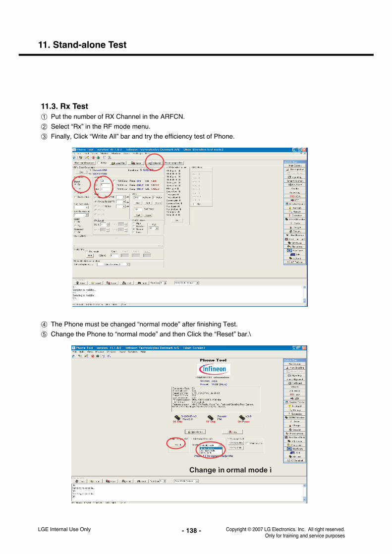
- 138 -
11. Stand-alone Test
11.3. Rx Test1 Put the number of RX Channel in the ARFCN.
2 Select “Rx” in the RF mode menu.
3 Finally, Click “Write All” bar and try the efficiency test of Phone.
4 The Phone must be changed “normal mode” after finishing Test.
5 Change the Phone to “normal mode” and then Click the “Reset” bar.\
LGE Internal Use Only Copyright © 2007 LG Electronics. Inc. All right reserved. Only for training and service purposes
Change ìn ormal mode ì

LGE Internal Use OnlyCopyright © 2007 LG Electronics. Inc. All right reserved. Only for training and service purposes
12. ENGINEERING MODE
- 139 -
12. ENGINEERING MODE
Engineering mode is designed to allow a service man/engineer to view and test the basic functions providedby a handset. The key sequence for switching the engineering mode on is “2945#*#” Select. Pressing ENDwill switch back to non-engineering mode operation. Use Up and Down key to select a menu and press‘select’ key to progress the test. Pressing ‘back key will switch back to the original test menu.
[1] BB TEST
[1-1] Battery Info
[1-1-1] BattInfo
[1-2] Bluetooth Test
[1-2-1] Enter Test Mode
[1-2-2] OnOff Test
[1-2-3] Headset Test
[1-2-4] BT Test1
[1-2-5] BT Test2
[1-2-6] Xhtml Compose Print
[1-2-7] Xhtml Print Test
[2] Model Version
[2-1] Version
[3] Eng Mode
[3-1] Cell environ.
[3-2] PS Layer Info
[3-2-1] Mobility
[3-2-2] RadioRes
[3-2-1] Gprs
[3-3] Layer1 Info
[3-4] Reset Information
[3-5] Memory Configurarion
[3-6] MemGenConf
[3-7] MemAllUse
[3-8] MemDetUse
[3-9] MemDump
[3-10] Change Frequency Band
[4] Call Timer
[6] MF TEST
[5] Factory Reset
[6-1] All Auto Test
[6-2] Backlight
[6-2-1] BacklightOn
[6-2-2] BacklightOff
[6-3] Audio
[6-3-1] Audio Test
[6-4] Vibrator
[6-4-1] VibratorOn
[6-4-2] VibratorOff
[6-5] LCD
[6-5-1] Auto LCD
[6-6] Key pad
[6-7] Mic Speaker
[6-8] Camera
[6-8-1] Camera Main Preview
[6-8-2] FlashOn
[6-8-3] FlashOff
[6-8-4] CameraFlashBunning
[6-9] FM Radio
[6-9-1] FM Radio Test
[6-10] Touchpad Test
[7] Network selection
[7-1] Automatic
[7-2] GSM850
[7-3] EGSM
[7-4] DCS
[7-5] PCS

LGE Internal Use Only Copyright © 2007 LG Electronics. Inc. All right reserved. Only for training and service purposes
- 140 -

- 141 -
12
3 5 6 8 10
11 13 1519
2024
25
3637 38
394042 46
51 52 53 54
5049
48
47
101
96959391
898785
8486 92 94
97
100
98
999081
8088
8379
7877
7673
74
75
7268
64
67
7170696159
575655
66
65
6362
5860
82
4544
4341
32302831 33
26
27
29
34
22
23
21
179
74
35
18161412
13. EXPLODED VIEW & REPLACEMENT PART LIST
13.1 EXPLODED VIEW
LGE Internal Use OnlyCopyright © 2007 LG Electronics. Inc. All right reserved. Only for training and service purposes

- 142 -
A
B
CD E
F
G
H
I J
K
ASS'Y EXPLODED VIEW
LGE Internal Use OnlyCopyright © 2007 LG Electronics. Inc. All right reserved. Only for training and service purposes
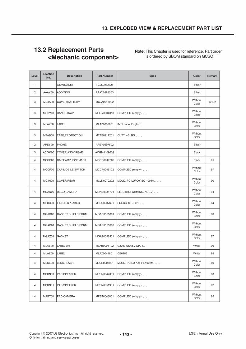
- 143 -
13. EXPLODED VIEW & REPLACEMENT PART LIST
LGE Internal Use OnlyCopyright © 2007 LG Electronics. Inc. All right reserved. Only for training and service purposes
13.2 Replacement Parts<Mechanic component>
LevelLocation
No.Description Part Number Spec Color Remark
1 GSM(SLIDE) TGLL0012326 Silver
2 AAAY00 ADDITION AAAY0283553 Silver
3 MCJA00 COVER,BATTERY MCJA0046902Without
Color101, K
3 MHBY00 HANDSTRAP MHBY0004310 COMPLEX, (empty), , , , ,Without
Color
3 MLAZ00 LABEL MLAZ0033601 IMEI Label,EnglishWithout
Color
3 MTAB00 TAPE,PROTECTION MTAB0217201 CUTTING, NS, , , , ,Without
Color
2 APEY00 PHONE APEY0597502 Silver
3 ACGM00 COVER ASSY,REAR ACGM0109602 Black
4 MCCC00 CAP,EARPHONE JACK MCCC0047002 COMPLEX, (empty), , , , , Black 91
4 MCCF00 CAP,MOBILE SWITCH MCCF0045102 COMPLEX, (empty), , , , ,Without
Color97
4 MCJN00 COVER,REAR MCJN0070202 MOLD, PC LUPOY SC-1004A, , , , ,Without
Color90
4 MDAD00 DECO,CAMERA MDAD0031701 ELECTROFORMING, Ni, 0.2, , , ,Without
Color94
4 MFBC00 FILTER,SPEAKER MFBC0032601 PRESS, STS, 0.1, , , ,Without
Color84
4 MGAD00 GASKET,SHIELD FORM MGAD0155301 COMPLEX, (empty), , , , ,Without
Color80
4 MGAD01 GASKET,SHIELD FORM MGAD0155302 COMPLEX, (empty), , , , ,Without
Color
4 MGAZ00 GASKET MGAZ0058501 COMPLEX, (empty), , , , ,Without
Color87
4 MLAB00 LABEL,A/S MLAB0001102 C2000 USASV DIA 4.0 White 99
4 MLAZ00 LABEL MLAZ0044801 CE0186 White 98
4 MLCE00 LENS,FLASH MLCE0007901 MOLD, PC LUPOY HI-1002M, , , , ,Without
Color89
4 MPBN00 PAD,SPEAKER MPBN0047301 COMPLEX, (empty), , , , ,Without
Color83
4 MPBN01 PAD,SPEAKER MPBN0051301 COMPLEX, (empty), , , , ,Without
Color82
4 MPBT00 PAD,CAMERA MPBT0043801 COMPLEX, (empty), , , , ,Without
Color85
Note: This Chapter is used for reference, Part orderis ordered by SBOM standard on GCSC

- 144 -
13. EXPLODED VIEW & REPLACEMENT PART LIST
LGE Internal Use Only Copyright © 2007 LG Electronics. Inc. All right reserved. Only for training and service purposes
LevelLocation
No.Description Part Number Spec Color Remark
4 MPBU00 PAD,CONNECTOR MPBU0011201 COMPLEX, (empty), , , , ,Without
Color86
4 MPFZ00 PLATE MPFZ0029801 PRESS, STS, 0.4, , , ,Without
Color81
4 MTAA00 TAPE,DECO MTAA0140201 COMPLEX, (empty), , , , ,Without
Color93
4 MTAB00 TAPE,PROTECTION MTAB0217301 COMPLEX, (empty), , , , ,Without
Color96
4 MTAD00 TAPE,WINDOW MTAD0071101 COMPLEX, (empty), , , , ,Without
Color92
4 MTAZ00 TAPE MTAZ0204101 COMPLEX, (empty), , , , ,Without
Color88
4 MWAE00 WINDOW,CAMERA MWAE0033301 CUTTING, NS, , , , , Black 95
3 ACGQ00 COVER ASSY,SLIDE ACGQ0019717Without
Color
4 ACGK00 COVER ASSY,FRONT ACGK0092302Without
ColorG
5 MBJC00 BUTTON,FUNCTION MBJC0022702 COMPLEX, (empty), , , , ,Without
Color59
5 MBJL00 BUTTON,SIDE MBJL0044702 COMPLEX, (empty), , , , , Black 58
5 MCJK00 COVER,FRONT MCJK0074102 MOLD, PC LUPOY SC-1004A, , , , ,Without
Color57
5 MDAG00 DECO,FRONT MDAG0029501 MOLD, POM LUCEL N109-LD, , , , , Black 55
5 MPBF00 PAD,FLEXIBLE PCB MPBF0023001 COMPLEX, (empty), , , , ,Without
Color67
5 MPBG00 PAD,LCD MPBG0073901 CUTTING, NS, , , , ,Without
Color
5 MPBN00 PAD,SPEAKER MPBN0052901 COMPLEX, (empty), , , , ,Without
Color63
5 MPBU00 PAD,CONNECTOR MPBU0011101 COMPLEX, (empty), , , , ,Without
Color65
5 MTAA00 TAPE,DECO MTAA0147601 COMPLEX, (empty), , , , ,Without
Color56
5 MTAF00 TAPE,MOTOR MTAF0013901 COMPLEX, (empty), 0.05, , , ,Without
Color62
5 MTAG00 TAPE,BUTTON MTAG0006101 COMPLEX, (empty), , , , ,Without
Color60
5 MTAG01 TAPE,BUTTON MTAG0006201 COMPLEX, (empty), , , , ,Without
Color61
5 MTAK00 TAPE,CAMERA MTAK0002001 COMPLEX, (empty), , , , ,Without
Color64
4 ACGR00COVERASSY,SLIDE(LOWER)
ACGR0011601Without
ColorE

LGE Internal Use OnlyCopyright © 2007 LG Electronics. Inc. All right reserved. Only for training and service purposes
13. EXPLODED VIEW & REPLACEMENT PART LIST
- 145 -
LevelLocation
No.Description Part Number Spec Color Remark
5 MCJV00 COVER,SLIDE(LOWER) MCJV0012101 CASTING, Mg Alloy, , , , ,Without
Color41
5 MGDA00 GUIDE,LEFT MGDA0011701 MOLD, POM LUCEL FW-700A, , , , , Black 44
5 MGDA01 GUIDE,LEFT MGDA0010601 MOLD, POM LUCEL N109-LD, , , , ,Without
Color45
5 MGDB00 GUIDE,RIGHT MGDB0006901 MOLD, POM LUCEL FW-700A, , , , , Black 43
5 MGDB01 GUIDE,RIGHT MGDB0005601 MOLD, POM LUCEL N109-LD, , , , ,Without
Color42
5 MIDZ00 INSULATOR MIDZ0163601 CUTTING, NS, , , , ,Without
Color31
5 MMAA00 MAGNET,SWITCH MMAA0009401 COMPLEX, (empty), , , , ,Without
Color34
5 MPBF00 PAD,FLEXIBLE PCB MPBF0022901 COMPLEX, (empty), , , , ,Without
Color40
5 MPBG00 PAD,LCD MPBG0063701 COMPLEX, (empty), , , , ,Without
Color33
5 MPBG01 PAD,LCD MPBG0074801 CUTTING, NS, , , , ,Without
Color29
5 MPBG02 PAD,LCD MPBG0074901 CUTTING, NS, , , , ,Without
Color30
5 MPBM00 PAD,RECEIVER MPBM0022201 CUTTING, NS, , , , ,Without
Color37
5 MPBU00 PAD,CONNECTOR MPBU0011301 COMPLEX, (empty), , , , ,Without
Color36
5 MPBZ00 PAD MPBZ0194501 CUTTING, NS, , , , , Black 32
5 MPBZ01 PAD MPBZ0199901 CUTTING, NS, , , , ,Without
Color38
5 MPBZ02 PAD MPBZ0194601 CUTTING, NS, , , , , Blue 39
5 MSGB00 STOPPER,HINGE MSGB0020801 MOLD, Urethane Rubber S190A, , , , ,Without
Color28
5 MTAZ00 TAPE MTAZ0196501 COMPLEX, (empty), , , , ,Without
Color35
4 ACGS00COVER ASSY,SLIDE(UPPER)
ACGS0013402 Silver B
5 MCJW00 COVER,SLIDE(UPPER) MCJW0014302 CASTING, Al Alloy, , , , , Silver 11
5 MDAE00 DECO,FOLDER(UPPER) MDAE0040401 PRESS, STS, 0.2, , , ,Without
Color4
5 MDAH00 DECO,RECEIVER MDAH0022301 PRESS, STS, 0.2, , , ,Without
Color3
5 MIDZ00 INSULATOR MIDZ0161901 CUTTING, NS, , , , ,Without
Color14

- 146 -
13. EXPLODED VIEW & REPLACEMENT PART LIST
LGE Internal Use Only Copyright © 2007 LG Electronics. Inc. All right reserved. Only for training and service purposes
LevelLocation
No.Description Part Number Spec Color Remark
5 MPBM00 PAD,RECEIVER MPBM0018901 COMPLEX, (empty), , , , ,Without
Color15
5 MPBZ00 PAD MPBZ0189101 COMPLEX, (empty), 0.3, , , ,Without
Color17
5 MPFZ00 PLATE MPFZ0030401 PRESS, STS, 0.1, , , ,Without
Color13
5 MTAA00 TAPE,DECO MTAA0140101 COMPLEX, (empty), , , , ,Without
Color6
5 MTAA01 TAPE,DECO MTAA0147801 COMPLEX, (empty), 0.2, , , ,Without
Color7
5 MTAB00 TAPE,PROTECTION MTAB0232101 COMPLEX, (empty), , , , ,Without
Color
5 MTAD00 TAPE,WINDOW MTAD0071001 COMPLEX, (empty), , , , ,Without
Color8
5 MTAE00 TAPE,WINDOW(SUB) MTAE0032401 COMPLEX, (empty), 0.2, , , ,Without
Color9
5 MTAZ00 TAPE MTAZ0196101 COMPLEX, (empty), 0.3, , , ,Without
Color10
5 MTAZ01 TAPE MTAZ0196201 COMPLEX, (empty), 0.05, , , ,Without
Color5
5 MTAZ03 TAPE MTAZ0196401 COMPLEX, (empty), 0.05, , , ,Without
Color12
5 MTAZ04 TAPE MTAZ0204701 CUTTING, NS, 0.05, , , ,Without
Color16
4 AKAC00 KEYPAD ASSY,MAIN AKAC0002601 ENGLISH Black 69, H
4 ARDY00 RAIL ASSY,SLIDE ARDY0003201 Black 46, F
4 GGZZ00 SCREW TAPPING GGZZ0002001 1.7 mm,2.2 mm,MSWR3(BK) ,B ,+ ,- , Black 47
4 GMEY02 SCREW MACHINE,BIND GMEY0017801Without
Color26, 68
4 GMEY03 SCREW MACHINE,BIND GMEY00192011.4 mm,1.8 mm,SWCH18A ,N ,+ , ,; ,[empty] ,+ , , ,CR-7,WHITE ,[empty] ,[empty]
WHITESILVER
48
4 MCCH00 CAP,SCREW MCCH0109501 COMPLEX, (empty), , , , ,Without
Color54
4 MCCH01 CAP,SCREW MCCH0109601 COMPLEX, (empty), , , , ,Without
Color52
4 MIDZ00 INSULATOR MIDZ0156801 CUTTING, NS, , , , ,Without
Color24
4 MIDZ01 INSULATOR MIDZ0156701 CUTTING, NS, , , , ,Without
Color50
4 MLAZ00 LABEL MLAZ0038303 PRINTING, (empty), , , , , White
4 MPBF00 PAD,FLEXIBLE PCB MPBF0030501 CUTTING, NS, , , , ,Without
Color23
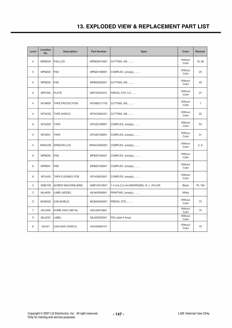
- 147 -
13. EXPLODED VIEW & REPLACEMENT PART LIST
LGE Internal Use OnlyCopyright © 2007 LG Electronics. Inc. All right reserved. Only for training and service purposes
LevelLocation
No.Description Part Number Spec Color Remark
4 MPBG00 PAD,LCD MPBG0073901 CUTTING, NS, , , , ,Without
Color18, 66
4 MPBZ00 PAD MPBZ0188901 COMPLEX, (empty), , , , ,Without
Color25
4 MPBZ02 PAD MPBZ0200001 CUTTING, NS, , , , ,Without
Color49
4 MPFZ00 PLATE MPFZ0029701 PRESS, STS, 0.2, , , ,Without
Color27
4 MTAB00 TAPE,PROTECTION MTAB0211703 CUTTING, NS, , , , ,Without
Color1
4 MTAC00 TAPE,SHIELD MTAC0064201 CUTTING, NS, , , , ,Without
Color22
4 MTAZ00 TAPE MTAZ0196801 COMPLEX, (empty), , , , ,Without
Color53
4 MTAZ01 TAPE MTAZ0196901 COMPLEX, (empty), , , , ,Without
Color51
4 MWAC00 WINDOW,LCD MWAC0082001 COMPLEX, (empty), , , , ,Without
Color2, A
6 MPBZ00 PAD MPBZ0189301 COMPLEX, (empty), , , , ,Without
Color
6 MPBZ01 PAD MPBZ0189001 COMPLEX, (empty), , , , ,Without
Color
6 MTAJ00 TAPE,FLEXIBLE PCB MTAJ0003001 COMPLEX, (empty), , , , ,Without
Color
3 GMEY00 SCREW MACHINE,BIND GMEY0010601 1.4 mm,2.5 mm,MSWR3(BK) ,N ,+ ,NYLOK Black 78, 100
3 MLAK00 LABEL,MODEL MLAK0006901 PRINTING, (empty), , , , , White
5 MCBA02 CAN,SHIELD MCBA0020001 PRESS, STS, , , , ,Without
Color72
7 ADCA00 DOME ASSY,METAL ADCA0075801Without
Color70
5 MLAZ00 LABEL MLAZ0038301 PID Label 4 ArrayWithout
Color
6 SC401 CAN ASSY,SHIELD ACKA0005101Without
Color75
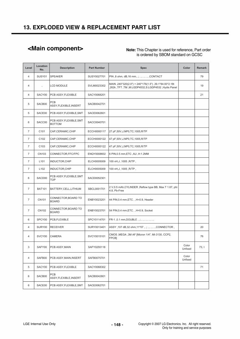
LGE Internal Use Only Copyright © 2007 LG Electronics. Inc. All right reserved. Only for training and service purposes
13. EXPLODED VIEW & REPLACEMENT PART LIST
- 148 -
LevelLocation
No.Description Part Number Spec Color Remark
4 SUSY01 SPEAKER SUSY0027701 PIN ,8 ohm, dB,16 mm, ,; , , , , , , ,CONTACT 79
4 .. LCD MODULE SVLM0023302MAIN ,240*320(2.0") + 240*176(1.5") ,39.1*84.93*2.18t,262k ,TFT ,TM ,M:LGDP4532,S:LGDP4532 ,Hydis Panel
19
4 SACY00 PCB ASSY,FLEXIBLE SACY0068201 21
5 SACB00PCBASSY,FLEXIBLE,INSERT
SACB0042701
5 SACE00 PCB ASSY,FLEXIBLE,SMT SACE0062601
6 SACC00PCB ASSY,FLEXIBLE,SMTBOTTOM
SACC0040701
7 C101 CAP,CERAMIC,CHIP ECCH0000117 27 pF,50V,J,NP0,TC,1005,R/TP
7 C102 CAP,CERAMIC,CHIP ECCH0000122 47 pF,50V,J,NP0,TC,1005,R/TP
7 C103 CAP,CERAMIC,CHIP ECCH0000122 47 pF,50V,J,NP0,TC,1005,R/TP
7 CN103 CONNECTOR,FFC/FPC ENQY0008602 6 PIN,0.5 mm,ETC ,AU ,H:1.2MM
7 L101 INDUCTOR,CHIP ELCH0005009 100 nH,J ,1005 ,R/TP ,
7 L102 INDUCTOR,CHIP ELCH0005009 100 nH,J ,1005 ,R/TP ,
6 SACD00PCB ASSY,FLEXIBLE,SMTTOP
SACD0052301
7 BAT101 BATTERY,CELL,LITHIUM SBCL00017012 V,0.5 mAh,CYLINDER ,Reflow type BB, Max T 1.67, phi4.8, Pb-Free
7 CN101CONNECTOR,BOARD TOBOARD
ENBY0023201 44 PIN,0.4 mm,ETC , ,H=0.9, Header
7 CN102CONNECTOR,BOARD TOBOARD
ENBY0023701 54 PIN,0.4 mm,ETC , ,H=0.9, Socket
6 SPCY00 PCB,FLEXIBLE SPCY0114701 FR-1 ,0.1 mm,DOUBLE , ,; , , , , , , , , ,
4 SURY00 RECEIVER SURY0013401 ASSY ,107 dB,32 ohm,11*07 , ,; , , , , , ,CONNECTOR , 20
4 SVCY00 CAMERA SVCY0015101CMOS ,MEGA ,3M AF [Micron 1/4", MI-3130, CCP2,FPCB]
76
3 SAFY00 PCB ASSY,MAIN SAFY0255118Color
Unfixed73, I
4 SAFB00 PCB ASSY,MAIN,INSERT SAFB0075701Color
Unfixed
5 SACY00 PCB ASSY,FLEXIBLE SACY0068302 71
6 SACB00PCBASSY,FLEXIBLE,INSERT
SACB0042801
6 SACE00 PCB ASSY,FLEXIBLE,SMT SACE0062701
<Main component> Note: This Chapter is used for reference, Part orderis ordered by SBOM standard on GCSC

- 149 -
13. EXPLODED VIEW & REPLACEMENT PART LIST
LGE Internal Use OnlyCopyright © 2007 LG Electronics. Inc. All right reserved. Only for training and service purposes
LevelLocation
No.Description Part Number Spec Color Remark
7 SACC00PCB ASSY,FLEXIBLE,SMTBOTTOM
SACC0040801
8 C102 CAP,CHIP,MAKER ECZH0003103 0.1 uF,10V ,K ,X7R ,HD ,1005 ,R/TP
8 C103 CAP,CHIP,MAKER ECZH0003103 0.1 uF,10V ,K ,X7R ,HD ,1005 ,R/TP
8 C104 CAP,CERAMIC,CHIP ECCH0000198 2.2 uF,6.3V ,M ,X5R ,TC ,1005 ,R/TP
8 C105 CAP,CHIP,MAKER ECZH0003103 0.1 uF,10V ,K ,X7R ,HD ,1005 ,R/TP
8 C106 CAP,CHIP,MAKER ECZH0003103 0.1 uF,10V ,K ,X7R ,HD ,1005 ,R/TP
8 C107 CAP,CERAMIC,CHIP ECCH0000117 27 pF,50V,J,NP0,TC,1005,R/TP
8 C108 CAP,CERAMIC,CHIP ECCH0000117 27 pF,50V,J,NP0,TC,1005,R/TP
8 C109 CAP,CERAMIC,CHIP ECCH0000117 27 pF,50V,J,NP0,TC,1005,R/TP
8 CN101CONNECTOR,BOARD TOBOARD
ENBY0016601 20 PIN,0.4 mm,STRAIGHT ,AU ,0.9 STACKING HEIGHT
8 L101 INDUCTOR,CHIP ELCH0005009 100 nH,J ,1005 ,R/TP ,
8 L102 INDUCTOR,CHIP ELCH0005009 100 nH,J ,1005 ,R/TP ,
8 MIC101 MICROPHONE SUMY0010602UNIT ,-42 dB,6.15*3.76*1.25 ,Silicon mic , ,-42 ,300,OMNI ,[empty] ,6.15*3.76*1.25 ,SMD
8 VA102 VARISTOR SEVY0003601 5.6 V, ,SMD ,100pF, 1005
8 VA103 VARISTOR SEVY0003601 5.6 V, ,SMD ,100pF, 1005
7 SACD00PCB ASSY,FLEXIBLE,SMTTOP
SACD0052401
8 AF_CAM SWITCH,TACT ESCY0004201 12 V,0.02 A,HORIZONTAL ,0.2 G,
8 C101 CAP,CERAMIC,CHIP ECCH0000198 2.2 uF,6.3V ,M ,X5R ,TC ,1005 ,R/TP
8 LD101 DIODE,LED,CHIP EDLH0013701WHITE ,ETC ,R/TP ,SIDEVIEW ,; ,[empty] ,2.9~3.75,30mA , , ,120mW ,[empty] ,[empty] ,2P
8 LD102 DIODE,LED,CHIP EDLH0013701WHITE ,ETC ,R/TP ,SIDEVIEW ,; ,[empty] ,2.9~3.75,30mA , , ,120mW ,[empty] ,[empty] ,2P
8 R102 RES,CHIP ERHY0003301 100 ohm,1/16W ,J ,1005 ,R/TP
8 R103 RES,CHIP ERHY0003301 100 ohm,1/16W ,J ,1005 ,R/TP
8 U101 IC EUSY0250001 Leaded ,4 PIN,R/TP ,Hall IC
7 SPCY00 PCB,FLEXIBLE SPCY0114801 POLYI ,0.15 mm,DOUBLE , ,; , , , , , , , , ,
5 SJMY00 VIBRATOR,MOTOR SJMY0008412 74
4 SAFF00 PCB ASSY,MAIN,SMT SAFF0171618
5 SAFC00PCB ASSY,MAIN,SMTBOTTOM
SAFC0101402Color
Unfixed
6 ANT402 ANTENNA,GSM,FIXED SNGF00322013.0 ,-2.0 dBd,, ,internal, bluetooth chip antenna ,;,SINGLE ,-2.0 ,50 ,3.0

- 150 -
13. EXPLODED VIEW & REPLACEMENT PART LIST
LGE Internal Use Only Copyright © 2007 LG Electronics. Inc. All right reserved. Only for training and service purposes
LevelLocation
No.Description Part Number Spec Color Remark
6 C207 CAP,CERAMIC,CHIP ECCH0004904 1 uF,6.3V ,K ,X5R ,TC ,1005 ,R/TP
6 C208 CAP,CERAMIC,CHIP ECCH0004904 1 uF,6.3V ,K ,X5R ,TC ,1005 ,R/TP
6 C216 CAP,CHIP,MAKER ECZH0000844 68 pF,50V ,J ,NP0 ,TC ,1005 ,R/TP
6 C217 CAP,CHIP,MAKER ECZH0000844 68 pF,50V ,J ,NP0 ,TC ,1005 ,R/TP
6 C219 CAP,CERAMIC,CHIP ECCH0000198 2.2 uF,6.3V ,M ,X5R ,TC ,1005 ,R/TP
6 C220 CAP,CERAMIC,CHIP ECCH0000198 2.2 uF,6.3V ,M ,X5R ,TC ,1005 ,R/TP
6 C221 CAP,CERAMIC,CHIP ECCH0000198 2.2 uF,6.3V ,M ,X5R ,TC ,1005 ,R/TP
6 C222 CAP,CERAMIC,CHIP ECCH0000117 27 pF,50V,J,NP0,TC,1005,R/TP
6 C223 CAP,CERAMIC,CHIP ECCH0000122 47 pF,50V,J,NP0,TC,1005,R/TP
6 C224 CAP,CERAMIC,CHIP ECCH0000122 47 pF,50V,J,NP0,TC,1005,R/TP
6 C230 CAP,CERAMIC,CHIP ECCH0004904 1 uF,6.3V ,K ,X5R ,TC ,1005 ,R/TP
6 C252 CAP,CERAMIC,CHIP ECCH0004904 1 uF,6.3V ,K ,X5R ,TC ,1005 ,R/TP
6 C254 CAP,CERAMIC,CHIP ECCH0004904 1 uF,6.3V ,K ,X5R ,TC ,1005 ,R/TP
6 C255 CAP,CERAMIC,CHIP ECCH0000117 27 pF,50V,J,NP0,TC,1005,R/TP
6 C256 CAP,CERAMIC,CHIP ECCH0000117 27 pF,50V,J,NP0,TC,1005,R/TP
6 C258 CAP,CHIP,MAKER ECZH0003103 0.1 uF,10V ,K ,X7R ,HD ,1005 ,R/TP
6 C259 CAP,CERAMIC,CHIP ECCH0005603 2.2 uF,10V ,K ,X5R ,TC ,1608 ,R/TP
6 C260 CAP,CERAMIC,CHIP ECCH0005603 2.2 uF,10V ,K ,X5R ,TC ,1608 ,R/TP
6 C261 CAP,CERAMIC,CHIP ECCH0000143 1 nF,50V,K,X7R,HD,1005,R/TP
6 C262 CAP,CERAMIC,CHIP ECCH0000122 47 pF,50V,J,NP0,TC,1005,R/TP
6 C263 CAP,CERAMIC,CHIP ECCH0000117 27 pF,50V,J,NP0,TC,1005,R/TP
6 C264 CAP,CERAMIC,CHIP ECCH0000110 10 pF,50V,D,NP0,TC,1005,R/TP
6 C265 CAP,CERAMIC,CHIP ECCH0004904 1 uF,6.3V ,K ,X5R ,TC ,1005 ,R/TP
6 C276 CAP,CERAMIC,CHIP ECCH0000155 10 nF,16V,K,X7R,HD,1005,R/TP
6 C284 CAP,CERAMIC,CHIP ECCH0000155 10 nF,16V,K,X7R,HD,1005,R/TP
6 C286 CAP,CERAMIC,CHIP ECCH0004904 1 uF,6.3V ,K ,X5R ,TC ,1005 ,R/TP
6 C304 CAP,CERAMIC,CHIP ECCH0000112 15 pF,50V,J,NP0,TC,1005,R/TP
6 C305 CAP,CERAMIC,CHIP ECCH0000112 15 pF,50V,J,NP0,TC,1005,R/TP
6 C306 CAP,CHIP,MAKER ECZH0001215 1 uF,10V ,K ,X5R ,TC ,1005 ,R/TP
6 C307 CAP,CHIP,MAKER ECZH0003103 0.1 uF,10V ,K ,X7R ,HD ,1005 ,R/TP
6 C308 CAP,CHIP,MAKER ECZH0003103 0.1 uF,10V ,K ,X7R ,HD ,1005 ,R/TP

- 151 -
13. EXPLODED VIEW & REPLACEMENT PART LIST
LGE Internal Use OnlyCopyright © 2007 LG Electronics. Inc. All right reserved. Only for training and service purposes
LevelLocation
No.Description Part Number Spec Color Remark
6 C309 CAP,CHIP,MAKER ECZH0000901 24 pF,50V ,J ,NP0 ,TC ,1005 ,R/TP
6 C310 CAP,CHIP,MAKER ECZH0003103 0.1 uF,10V ,K ,X7R ,HD ,1005 ,R/TP
6 C311 CAP,CHIP,MAKER ECZH0003103 0.1 uF,10V ,K ,X7R ,HD ,1005 ,R/TP
6 C312 CAP,CERAMIC,CHIP ECCH0000391 1 uF,50V ,Z ,Y5V ,HD ,2012 ,R/TP
6 C313 CAP,CERAMIC,CHIP ECCH0005604 10 uF,6.3V ,M ,X5R ,TC ,1608 ,R/TP
6 C314 CAP,CHIP,MAKER ECZH0000813 100 pF,50V ,J ,NP0 ,TC ,1005 ,R/TP
6 C315 CAP,CERAMIC,CHIP ECCH0000117 27 pF,50V,J,NP0,TC,1005,R/TP
6 C316 CAP,CERAMIC,CHIP ECCH0000117 27 pF,50V,J,NP0,TC,1005,R/TP
6 C317 CAP,CHIP,MAKER ECZH0003103 0.1 uF,10V ,K ,X7R ,HD ,1005 ,R/TP
6 C318 CAP,CERAMIC,CHIP ECCH0000120 39 pF,50V,J,NP0,TC,1005,R/TP
6 C319 CAP,CHIP,MAKER ECZH0001215 1 uF,10V ,K ,X5R ,TC ,1005 ,R/TP
6 C320 CAP,CERAMIC,CHIP ECCH0005604 10 uF,6.3V ,M ,X5R ,TC ,1608 ,R/TP
6 C321 CAP,CHIP,MAKER ECZH0000901 24 pF,50V ,J ,NP0 ,TC ,1005 ,R/TP
6 C322 CAP,CERAMIC,CHIP ECCH0005604 10 uF,6.3V ,M ,X5R ,TC ,1608 ,R/TP
6 C323 CAP,CHIP,MAKER ECZH0003103 0.1 uF,10V ,K ,X7R ,HD ,1005 ,R/TP
6 C335 CAP,CHIP,MAKER ECZH0001215 1 uF,10V ,K ,X5R ,TC ,1005 ,R/TP
6 C336 CAP,CERAMIC,CHIP ECCH0000198 2.2 uF,6.3V ,M ,X5R ,TC ,1005 ,R/TP
6 C337 CAP,CERAMIC,CHIP ECCH0000198 2.2 uF,6.3V ,M ,X5R ,TC ,1005 ,R/TP
6 C401 CAP,CHIP,MAKER ECZH0000813 100 pF,50V ,J ,NP0 ,TC ,1005 ,R/TP
6 C402 CAP,CHIP,MAKER ECZH0000813 100 pF,50V ,J ,NP0 ,TC ,1005 ,R/TP
6 C404 CAP,CERAMIC,CHIP ECCH0000115 22 pF,50V,J,NP0,TC,1005,R/TP
6 C405 INDUCTOR,CHIP ELCH0004727 100 nH,J ,1005 ,R/TP ,
6 C410 INDUCTOR,CHIP ELCH0001402 18 nH,J ,1005 ,R/TP ,Pb Free
6 C411 CAP,CERAMIC,CHIP ECCH0000701 1.2 pF,50V ,C ,NP0 ,TC ,1005 ,R/TP
6 C412 CAP,TANTAL,CHIP ECTH000570668 uF,6.3V ,M ,L_ESR ,3216 ,R/TP ,; , ,[empty] ,[empty] ,,[empty] , ,[empty] ,[empty] ,[empty] ,[empty]
6 C413 CAP,CHIP,MAKER ECZH0000813 100 pF,50V ,J ,NP0 ,TC ,1005 ,R/TP
6 C414 CAP,CERAMIC,CHIP ECCH0000901 2.2 pF,50V ,C ,NP0 ,TC ,1005 ,R/TP
6 C415 CAP,CERAMIC,CHIP ECCH0000901 2.2 pF,50V ,C ,NP0 ,TC ,1005 ,R/TP
6 C416 CAP,CERAMIC,CHIP ECCH0000901 2.2 pF,50V ,C ,NP0 ,TC ,1005 ,R/TP
6 C417 CAP,CERAMIC,CHIP ECCH0000901 2.2 pF,50V ,C ,NP0 ,TC ,1005 ,R/TP
6 C418 CAP,CERAMIC,CHIP ECCH0000175 2.7 pF,50V ,B ,NP0 ,TC ,1005 ,R/TP

- 152 -
13. EXPLODED VIEW & REPLACEMENT PART LIST
LGE Internal Use Only Copyright © 2007 LG Electronics. Inc. All right reserved. Only for training and service purposes
LevelLocation
No.Description Part Number Spec Color Remark
6 C419 CAP,CERAMIC,CHIP ECCH0000175 2.7 pF,50V ,B ,NP0 ,TC ,1005 ,R/TP
6 C420 CAP,CERAMIC,CHIP ECCH0000183 1.8 pF,50V ,C ,NP0 ,TC ,1005 ,R/TP
6 C421 CAP,CERAMIC,CHIP ECCH0000183 1.8 pF,50V ,C ,NP0 ,TC ,1005 ,R/TP
6 C422 CAP,CHIP,MAKER ECZH0003103 0.1 uF,10V ,K ,X7R ,HD ,1005 ,R/TP
6 C424 CAP,CHIP,MAKER ECZH0003103 0.1 uF,10V ,K ,X7R ,HD ,1005 ,R/TP
6 C425 CAP,CHIP,MAKER ECZH0001215 1 uF,10V ,K ,X5R ,TC ,1005 ,R/TP
6 C426 CAP,CERAMIC,CHIP ECCH0000117 27 pF,50V,J,NP0,TC,1005,R/TP
6 C427 CAP,CHIP,MAKER ECZH0000813 100 pF,50V ,J ,NP0 ,TC ,1005 ,R/TP
6 C428 CAP,CHIP,MAKER ECZH0000813 100 pF,50V ,J ,NP0 ,TC ,1005 ,R/TP
6 C429 CAP,CHIP,MAKER ECZH0001126 820 pF,50V ,K ,X7R ,HD ,1005 ,R/TP
6 C430 CAP,CHIP,MAKER ECZH0003103 0.1 uF,10V ,K ,X7R ,HD ,1005 ,R/TP
6 C431 CAP,CHIP,MAKER ECZH0003103 0.1 uF,10V ,K ,X7R ,HD ,1005 ,R/TP
6 C432 CAP,CHIP,MAKER ECZH0003103 0.1 uF,10V ,K ,X7R ,HD ,1005 ,R/TP
6 C433 CAP,CHIP,MAKER ECZH0003103 0.1 uF,10V ,K ,X7R ,HD ,1005 ,R/TP
6 C434 CAP,CERAMIC,CHIP ECCH0000163 47 nF,10V,K,X5R,HD,1005,R/TP
6 C435 CAP,CERAMIC,CHIP ECCH0000143 1 nF,50V,K,X7R,HD,1005,R/TP
6 C436 CAP,CHIP,MAKER ECZH0001216 220 nF,10V ,K ,X5R ,TC ,1005 ,R/TP
6 C438 CAP,CERAMIC,CHIP ECCH0000143 1 nF,50V,K,X7R,HD,1005,R/TP
6 C439 CAP,CERAMIC,CHIP ECCH0000155 10 nF,16V,K,X7R,HD,1005,R/TP
6 C443 CAP,CHIP,MAKER ECZH0001216 220 nF,10V ,K ,X5R ,TC ,1005 ,R/TP
6 C444 CAP,CHIP,MAKER ECZH0003103 0.1 uF,10V ,K ,X7R ,HD ,1005 ,R/TP
6 C445 CAP,CHIP,MAKER ECZH0003103 0.1 uF,10V ,K ,X7R ,HD ,1005 ,R/TP
6 C446 CAP,CERAMIC,CHIP ECCH0004904 1 uF,6.3V ,K ,X5R ,TC ,1005 ,R/TP
6 CN202 CONNECTOR,ETC ENZY0016301 3 PIN,3.0 mm,ETC , ,H-2.0
6 CN301CONNECTOR,BOARD TOBOARD
ENBY0016601 20 PIN,0.4 mm,STRAIGHT ,AU ,0.9 STACKING HEIGHT
6 CN302 CONNECTOR,I/O ENRY0006401 18 PIN,0.4 mm,ANGLE , ,H=2.5, Reverse Type
6 FB301 FILTER,BEAD,CHIP SFBH0007102 10 ohm,1005 ,Ferrite Bead
6 FB302 FILTER,BEAD,CHIP SFBH00081031000 ohm,1005 ,chip bead, 200mA,DCR0.9ohm ,; , ,,SMD ,R/TP
6 FL301 FILTER,EMI/POWER SFEY0007101 SMD ,1CH,1608Feedthru ESD/EMI filter for power Pb-free
6 FL302 VARISTOR SEVY0008302 5.5 V,30% ,SMD ,1409Size (4CH)

- 153 -
13. EXPLODED VIEW & REPLACEMENT PART LIST
LGE Internal Use OnlyCopyright © 2007 LG Electronics. Inc. All right reserved. Only for training and service purposes
LevelLocation
No.Description Part Number Spec Color Remark
6 FL303 VARISTOR SEVY0008302 5.5 V,30% ,SMD ,1409Size (4CH)
6 FL401 FILTER,SEPERATOR SFAY0011401850.900 ,1800.1900 , dB, dB, dB, dB,4532 ,GSM Quadband FEM.
6 L202 INDUCTOR,CHIP ELCH0005009 100 nH,J ,1005 ,R/TP ,
6 L203 INDUCTOR,CHIP ELCH0005009 100 nH,J ,1005 ,R/TP ,
6 L302 INDUCTOR,CHIP ELCH0005009 100 nH,J ,1005 ,R/TP ,
6 L303 INDUCTOR,CHIP ELCH0005009 100 nH,J ,1005 ,R/TP ,
6 L304 INDUCTOR,CHIP ELCH0005009 100 nH,J ,1005 ,R/TP ,
6 L305 INDUCTOR,CHIP ELCH0010302 100 nH,J ,1608 ,R/TP ,chip coil
6 L401 INDUCTOR,CHIP ELCH0001402 18 nH,J ,1005 ,R/TP ,Pb Free
6 L402 INDUCTOR,CHIP ELCH0009105 18 nH,J ,1005 ,R/TP ,COIL
6 L403 INDUCTOR,CHIP ELCH0009110 5.1 nH,J ,1005 ,R/TP ,chip coil
6 L404 INDUCTOR,CHIP ELCH0009110 5.1 nH,J ,1005 ,R/TP ,chip coil
6 LD201 DIODE,LED,MODULE EDLM0008806 WHITE ,1 LED,3.5x2.8x1.2t ,R/TP ,high power
6 Q203 TR,BJT,NPN EQBN0012401 ESM ,100 mW,R/TP ,NPN TRANSISTOR
6 R203 RES,CHIP,MAKER ERHZ0000444 22 Kohm,1/16W ,J ,1005 ,R/TP
6 R205 RES,CHIP,MAKER ERHZ0000444 22 Kohm,1/16W ,J ,1005 ,R/TP
6 R214 RES,CHIP,MAKER ERHZ0000485 4700 ohm,1/16W ,J ,1005 ,R/TP
6 R215 RES,CHIP,MAKER ERHZ0000406 100 Kohm,1/16W ,J ,1005 ,R/TP
6 R216 RES,CHIP,MAKER ERHZ0000406 100 Kohm,1/16W ,J ,1005 ,R/TP
6 R217 RES,CHIP,MAKER ERHZ0000406 100 Kohm,1/16W ,J ,1005 ,R/TP
6 R218 RES,CHIP,MAKER ERHZ0000406 100 Kohm,1/16W ,J ,1005 ,R/TP
6 R219 RES,CHIP,MAKER ERHZ0000406 100 Kohm,1/16W ,J ,1005 ,R/TP
6 R220 RES,CHIP,MAKER ERHZ0000406 100 Kohm,1/16W ,J ,1005 ,R/TP
6 R221 RES,CHIP,MAKER ERHZ0000483 47 ohm,1/16W ,J ,1005 ,R/TP
6 R222 RES,CHIP,MAKER ERHZ0000406 100 Kohm,1/16W ,J ,1005 ,R/TP
6 R226 RES,CHIP ERHY0011901 47 mohm,1/4W ,F ,2012 ,R/TP
6 R238 RES,CHIP,MAKER ERHZ0000331 110 Kohm,1/16W ,F ,1005 ,R/TP
6 R240 RES,CHIP,MAKER ERHZ0000530 5.1 Kohm,1/16W ,J ,1005 ,R/TP
6 R242 RES,CHIP,MAKER ERHZ0000404 1 Kohm,1/16W ,J ,1005 ,R/TP
6 R243 RES,CHIP,MAKER ERHZ0000493 51 Kohm,1/16W ,J ,1005 ,R/TP
6 R245 RES,CHIP,MAKER ERHZ0000493 51 Kohm,1/16W ,J ,1005 ,R/TP

- 154 -
13. EXPLODED VIEW & REPLACEMENT PART LIST
LGE Internal Use Only Copyright © 2007 LG Electronics. Inc. All right reserved. Only for training and service purposes
LevelLocation
No.Description Part Number Spec Color Remark
6 R246 RES,CHIP,MAKER ERHZ0000308 62 Kohm,1/16W ,F ,1005 ,R/TP
6 R247 RES,CHIP,MAKER ERHZ0000518 910 ohm,1/16W ,J ,1005 ,R/TP
6 R250 RES,CHIP,MAKER ERHZ0000213 120 Kohm,1/16W ,F ,1005 ,R/TP
6 R253 RES,CHIP,MAKER ERHZ0000406 100 Kohm,1/16W ,J ,1005 ,R/TP
6 R275 RES,CHIP,MAKER ERHZ0000444 22 Kohm,1/16W ,J ,1005 ,R/TP
6 R276 RES,CHIP,MAKER ERHZ0000444 22 Kohm,1/16W ,J ,1005 ,R/TP
6 R302 RES,CHIP,MAKER ERHZ0000406 100 Kohm,1/16W ,J ,1005 ,R/TP
6 R304 RES,CHIP ERHY0003301 100 ohm,1/16W ,J ,1005 ,R/TP
6 R306 RES,CHIP,MAKER ERHZ0000529 1.5 Kohm,1/16W ,J ,1005 ,R/TP
6 R307 RES,CHIP,MAKER ERHZ0000443 2200 ohm,1/16W ,J ,1005 ,R/TP
6 R308 RES,CHIP,MAKER ERHZ0000405 10 Kohm,1/16W ,J ,1005 ,R/TP
6 R309 RES,CHIP,MAKER ERHZ0000405 10 Kohm,1/16W ,J ,1005 ,R/TP
6 R310 RES,CHIP,MAKER ERHZ0000405 10 Kohm,1/16W ,J ,1005 ,R/TP
6 R311 RES,CHIP,MAKER ERHZ0000405 10 Kohm,1/16W ,J ,1005 ,R/TP
6 R313 RES,CHIP,MAKER ERHZ0000483 47 ohm,1/16W ,J ,1005 ,R/TP
6 R314 RES,CHIP,MAKER ERHZ0000485 4700 ohm,1/16W ,J ,1005 ,R/TP
6 R315 RES,CHIP,MAKER ERHZ0000485 4700 ohm,1/16W ,J ,1005 ,R/TP
6 R316 RES,CHIP,MAKER ERHZ0000483 47 ohm,1/16W ,J ,1005 ,R/TP
6 R317 RES,CHIP,MAKER ERHZ0000483 47 ohm,1/16W ,J ,1005 ,R/TP
6 R319 RES,CHIP,MAKER ERHZ0000483 47 ohm,1/16W ,J ,1005 ,R/TP
6 R320 RES,CHIP,MAKER ERHZ0000483 47 ohm,1/16W ,J ,1005 ,R/TP
6 R322 RES,CHIP,MAKER ERHZ0000485 4700 ohm,1/16W ,J ,1005 ,R/TP
6 R323 RES,CHIP,MAKER ERHZ0000405 10 Kohm,1/16W ,J ,1005 ,R/TP
6 R326 RES,CHIP,MAKER ERHZ0000463 33 ohm,1/16W ,J ,1005 ,R/TP
6 R328 RES,CHIP,MAKER ERHZ0000463 33 ohm,1/16W ,J ,1005 ,R/TP
6 R329 RES,CHIP,MAKER ERHZ0000485 4700 ohm,1/16W ,J ,1005 ,R/TP
6 R330 RES,CHIP,MAKER ERHZ0000485 4700 ohm,1/16W ,J ,1005 ,R/TP
6 R331 FILTER,BEAD,CHIP SFBH00081031000 ohm,1005 ,chip bead, 200mA,DCR0.9ohm ,; , ,,SMD ,R/TP
6 R332 FILTER,BEAD,CHIP SFBH00081031000 ohm,1005 ,chip bead, 200mA,DCR0.9ohm ,; , ,,SMD ,R/TP
6 R334 RES,CHIP,MAKER ERHZ0000406 100 Kohm,1/16W ,J ,1005 ,R/TP
6 R401 RES,CHIP ERHY0003301 100 ohm,1/16W ,J ,1005 ,R/TP
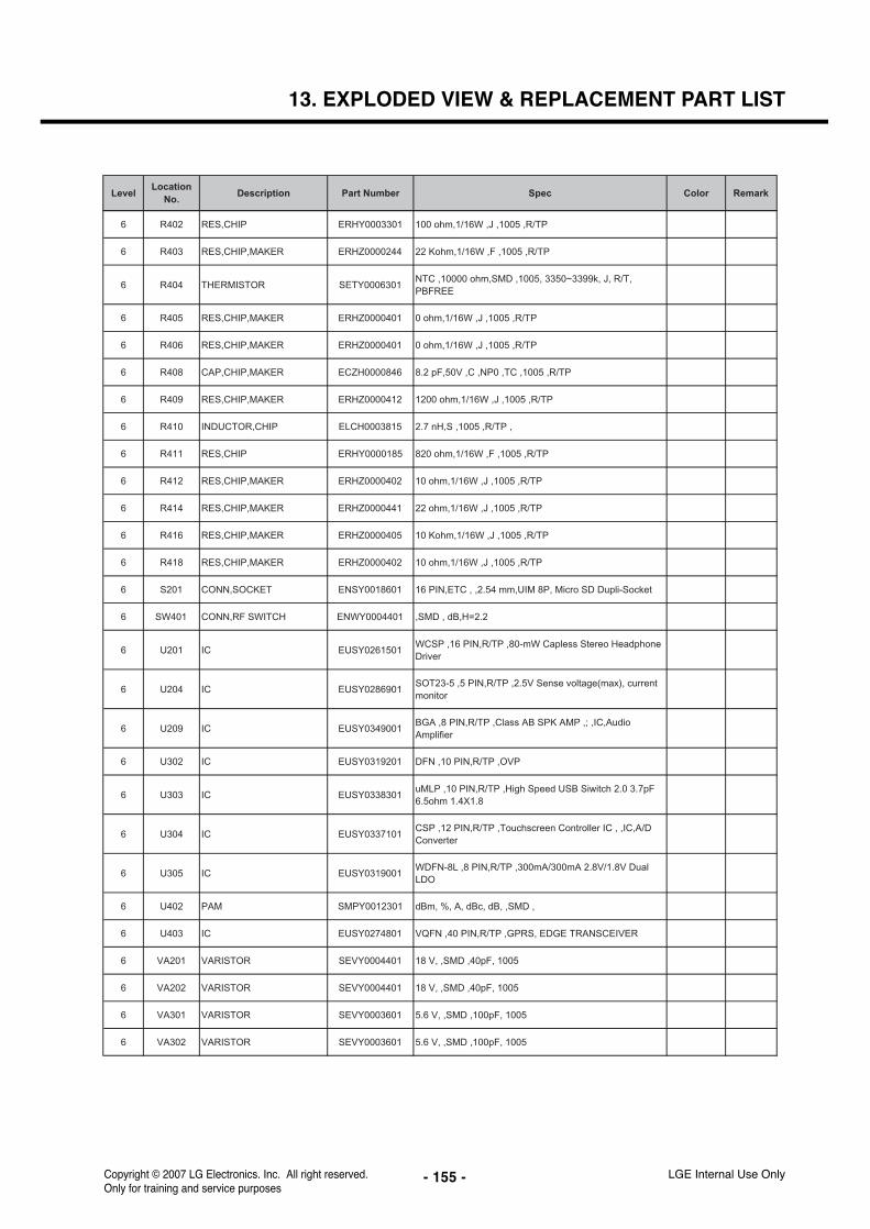
- 155 -
13. EXPLODED VIEW & REPLACEMENT PART LIST
LGE Internal Use OnlyCopyright © 2007 LG Electronics. Inc. All right reserved. Only for training and service purposes
LevelLocation
No.Description Part Number Spec Color Remark
6 R402 RES,CHIP ERHY0003301 100 ohm,1/16W ,J ,1005 ,R/TP
6 R403 RES,CHIP,MAKER ERHZ0000244 22 Kohm,1/16W ,F ,1005 ,R/TP
6 R404 THERMISTOR SETY0006301NTC ,10000 ohm,SMD ,1005, 3350~3399k, J, R/T,PBFREE
6 R405 RES,CHIP,MAKER ERHZ0000401 0 ohm,1/16W ,J ,1005 ,R/TP
6 R406 RES,CHIP,MAKER ERHZ0000401 0 ohm,1/16W ,J ,1005 ,R/TP
6 R408 CAP,CHIP,MAKER ECZH0000846 8.2 pF,50V ,C ,NP0 ,TC ,1005 ,R/TP
6 R409 RES,CHIP,MAKER ERHZ0000412 1200 ohm,1/16W ,J ,1005 ,R/TP
6 R410 INDUCTOR,CHIP ELCH0003815 2.7 nH,S ,1005 ,R/TP ,
6 R411 RES,CHIP ERHY0000185 820 ohm,1/16W ,F ,1005 ,R/TP
6 R412 RES,CHIP,MAKER ERHZ0000402 10 ohm,1/16W ,J ,1005 ,R/TP
6 R414 RES,CHIP,MAKER ERHZ0000441 22 ohm,1/16W ,J ,1005 ,R/TP
6 R416 RES,CHIP,MAKER ERHZ0000405 10 Kohm,1/16W ,J ,1005 ,R/TP
6 R418 RES,CHIP,MAKER ERHZ0000402 10 ohm,1/16W ,J ,1005 ,R/TP
6 S201 CONN,SOCKET ENSY0018601 16 PIN,ETC , ,2.54 mm,UIM 8P, Micro SD Dupli-Socket
6 SW401 CONN,RF SWITCH ENWY0004401 ,SMD , dB,H=2.2
6 U201 IC EUSY0261501WCSP ,16 PIN,R/TP ,80-mW Capless Stereo HeadphoneDriver
6 U204 IC EUSY0286901SOT23-5 ,5 PIN,R/TP ,2.5V Sense voltage(max), currentmonitor
6 U209 IC EUSY0349001BGA ,8 PIN,R/TP ,Class AB SPK AMP ,; ,IC,AudioAmplifier
6 U302 IC EUSY0319201 DFN ,10 PIN,R/TP ,OVP
6 U303 IC EUSY0338301uMLP ,10 PIN,R/TP ,High Speed USB Siwitch 2.0 3.7pF6.5ohm 1.4X1.8
6 U304 IC EUSY0337101CSP ,12 PIN,R/TP ,Touchscreen Controller IC , ,IC,A/DConverter
6 U305 IC EUSY0319001WDFN-8L ,8 PIN,R/TP ,300mA/300mA 2.8V/1.8V DualLDO
6 U402 PAM SMPY0012301 dBm, %, A, dBc, dB, ,SMD ,
6 U403 IC EUSY0274801 VQFN ,40 PIN,R/TP ,GPRS, EDGE TRANSCEIVER
6 VA201 VARISTOR SEVY0004401 18 V, ,SMD ,40pF, 1005
6 VA202 VARISTOR SEVY0004401 18 V, ,SMD ,40pF, 1005
6 VA301 VARISTOR SEVY0003601 5.6 V, ,SMD ,100pF, 1005
6 VA302 VARISTOR SEVY0003601 5.6 V, ,SMD ,100pF, 1005

- 156 -
13. EXPLODED VIEW & REPLACEMENT PART LIST
LGE Internal Use Only Copyright © 2007 LG Electronics. Inc. All right reserved. Only for training and service purposes
LevelLocation
No.Description Part Number Spec Color Remark
6 X401 VCTCXO EXSK000820126 MHz,2 PPM, pF,SMD ,32*25*10.5 , ,; , ,2PPM ,2.85V,32 ,25 ,10.5 , ,SMD ,P/TP
5 SAFD00 PCB ASSY,MAIN,SMT TOP SAFD0100202
6 C101 CAP,CERAMIC,CHIP ECCH0004904 1 uF,6.3V ,K ,X5R ,TC ,1005 ,R/TP
6 C102 CAP,CHIP,MAKER ECZH0003103 0.1 uF,10V ,K ,X7R ,HD ,1005 ,R/TP
6 C103 CAP,CERAMIC,CHIP ECCH0000155 10 nF,16V,K,X7R,HD,1005,R/TP
6 C104 CAP,CERAMIC,CHIP ECCH0004904 1 uF,6.3V ,K ,X5R ,TC ,1005 ,R/TP
6 C105 CAP,CHIP,MAKER ECZH0003103 0.1 uF,10V ,K ,X7R ,HD ,1005 ,R/TP
6 C106 CAP,CERAMIC,CHIP ECCH0000155 10 nF,16V,K,X7R,HD,1005,R/TP
6 C107 CAP,CERAMIC,CHIP ECCH0004904 1 uF,6.3V ,K ,X5R ,TC ,1005 ,R/TP
6 C108 CAP,CHIP,MAKER ECZH0003103 0.1 uF,10V ,K ,X7R ,HD ,1005 ,R/TP
6 C109 CAP,CHIP,MAKER ECZH0003103 0.1 uF,10V ,K ,X7R ,HD ,1005 ,R/TP
6 C110 CAP,CHIP,MAKER ECZH0003103 0.1 uF,10V ,K ,X7R ,HD ,1005 ,R/TP
6 C111 CAP,CHIP,MAKER ECZH0003103 0.1 uF,10V ,K ,X7R ,HD ,1005 ,R/TP
6 C112 CAP,CHIP,MAKER ECZH0003103 0.1 uF,10V ,K ,X7R ,HD ,1005 ,R/TP
6 C113 CAP,CHIP,MAKER ECZH0003103 0.1 uF,10V ,K ,X7R ,HD ,1005 ,R/TP
6 C114 CAP,CHIP,MAKER ECZH0003103 0.1 uF,10V ,K ,X7R ,HD ,1005 ,R/TP
6 C115 CAP,CHIP,MAKER ECZH0003103 0.1 uF,10V ,K ,X7R ,HD ,1005 ,R/TP
6 C116 CAP,CHIP,MAKER ECZH0003103 0.1 uF,10V ,K ,X7R ,HD ,1005 ,R/TP
6 C117 CAP,CHIP,MAKER ECZH0003103 0.1 uF,10V ,K ,X7R ,HD ,1005 ,R/TP
6 C118 CAP,CHIP,MAKER ECZH0003103 0.1 uF,10V ,K ,X7R ,HD ,1005 ,R/TP
6 C119 CAP,CHIP,MAKER ECZH0003103 0.1 uF,10V ,K ,X7R ,HD ,1005 ,R/TP
6 C121 CAP,CERAMIC,CHIP ECCH0004904 1 uF,6.3V ,K ,X5R ,TC ,1005 ,R/TP
6 C122 CAP,CHIP,MAKER ECZH0003103 0.1 uF,10V ,K ,X7R ,HD ,1005 ,R/TP
6 C123 CAP,CHIP,MAKER ECZH0003103 0.1 uF,10V ,K ,X7R ,HD ,1005 ,R/TP
6 C124 CAP,CERAMIC,CHIP ECCH0004904 1 uF,6.3V ,K ,X5R ,TC ,1005 ,R/TP
6 C125 CAP,CHIP,MAKER ECZH0003103 0.1 uF,10V ,K ,X7R ,HD ,1005 ,R/TP
6 C126 CAP,CHIP,MAKER ECZH0003103 0.1 uF,10V ,K ,X7R ,HD ,1005 ,R/TP
6 C127 CAP,CHIP,MAKER ECZH0003103 0.1 uF,10V ,K ,X7R ,HD ,1005 ,R/TP
6 C128 CAP,CHIP,MAKER ECZH0003103 0.1 uF,10V ,K ,X7R ,HD ,1005 ,R/TP
6 C129 CAP,CHIP,MAKER ECZH0003103 0.1 uF,10V ,K ,X7R ,HD ,1005 ,R/TP
6 C130 CAP,CHIP,MAKER ECZH0003103 0.1 uF,10V ,K ,X7R ,HD ,1005 ,R/TP

- 157 -
13. EXPLODED VIEW & REPLACEMENT PART LIST
LGE Internal Use OnlyCopyright © 2007 LG Electronics. Inc. All right reserved. Only for training and service purposes
LevelLocation
No.Description Part Number Spec Color Remark
6 C131 CAP,CHIP,MAKER ECZH0003103 0.1 uF,10V ,K ,X7R ,HD ,1005 ,R/TP
6 C132 CAP,CHIP,MAKER ECZH0003103 0.1 uF,10V ,K ,X7R ,HD ,1005 ,R/TP
6 C133 CAP,CHIP,MAKER ECZH0001216 220 nF,10V ,K ,X5R ,TC ,1005 ,R/TP
6 C134 CAP,CERAMIC,CHIP ECCH0000112 15 pF,50V,J,NP0,TC,1005,R/TP
6 C135 CAP,CERAMIC,CHIP ECCH0000112 15 pF,50V,J,NP0,TC,1005,R/TP
6 C136 CAP,CERAMIC,CHIP ECCH0000143 1 nF,50V,K,X7R,HD,1005,R/TP
6 C137 CAP,CERAMIC,CHIP ECCH0000117 27 pF,50V,J,NP0,TC,1005,R/TP
6 C138 CAP,CERAMIC,CHIP ECCH0000117 27 pF,50V,J,NP0,TC,1005,R/TP
6 C139 CAP,CERAMIC,CHIP ECCH0000117 27 pF,50V,J,NP0,TC,1005,R/TP
6 C140 CAP,CERAMIC,CHIP ECCH0000117 27 pF,50V,J,NP0,TC,1005,R/TP
6 C201 CAP,CERAMIC,CHIP ECCH0000198 2.2 uF,6.3V ,M ,X5R ,TC ,1005 ,R/TP
6 C202 CAP,CERAMIC,CHIP ECCH0000198 2.2 uF,6.3V ,M ,X5R ,TC ,1005 ,R/TP
6 C203 CAP,CERAMIC,CHIP ECCH0000198 2.2 uF,6.3V ,M ,X5R ,TC ,1005 ,R/TP
6 C204 CAP,CERAMIC,CHIP ECCH0000198 2.2 uF,6.3V ,M ,X5R ,TC ,1005 ,R/TP
6 C205 CAP,CERAMIC,CHIP ECCH0000198 2.2 uF,6.3V ,M ,X5R ,TC ,1005 ,R/TP
6 C206 CAP,TANTAL,CHIP ECTH0005702100 uF,6.3V ,M ,L_ESR ,3216 ,R/TP ,; , ,[empty] ,[empty], ,[empty] , ,[empty] ,[empty] ,[empty] ,[empty]
6 C209 CAP,CERAMIC,CHIP ECCH0004904 1 uF,6.3V ,K ,X5R ,TC ,1005 ,R/TP
6 C210 CAP,CERAMIC,CHIP ECCH0000198 2.2 uF,6.3V ,M ,X5R ,TC ,1005 ,R/TP
6 C211 CAP,CERAMIC,CHIP ECCH0000198 2.2 uF,6.3V ,M ,X5R ,TC ,1005 ,R/TP
6 C212 CAP,CHIP,MAKER ECZH0003103 0.1 uF,10V ,K ,X7R ,HD ,1005 ,R/TP
6 C213 CAP,CERAMIC,CHIP ECCH0004904 1 uF,6.3V ,K ,X5R ,TC ,1005 ,R/TP
6 C214 CAP,CERAMIC,CHIP ECCH0004904 1 uF,6.3V ,K ,X5R ,TC ,1005 ,R/TP
6 C215 CAP,CHIP,MAKER ECZH0003103 0.1 uF,10V ,K ,X7R ,HD ,1005 ,R/TP
6 C218 CAP,CERAMIC,CHIP ECCH0004904 1 uF,6.3V ,K ,X5R ,TC ,1005 ,R/TP
6 C225 CAP,CHIP,MAKER ECZH0000813 100 pF,50V ,J ,NP0 ,TC ,1005 ,R/TP
6 C226 CAP,CHIP,MAKER ECZH0000813 100 pF,50V ,J ,NP0 ,TC ,1005 ,R/TP
6 C227 CAP,CERAMIC,CHIP ECCH0000198 2.2 uF,6.3V ,M ,X5R ,TC ,1005 ,R/TP
6 C228 CAP,CERAMIC,CHIP ECCH0000198 2.2 uF,6.3V ,M ,X5R ,TC ,1005 ,R/TP
6 C229 CAP,CERAMIC,CHIP ECCH0000198 2.2 uF,6.3V ,M ,X5R ,TC ,1005 ,R/TP
6 C231 CAP,CERAMIC,CHIP ECCH0005604 10 uF,6.3V ,M ,X5R ,TC ,1608 ,R/TP
6 C232 CAP,CERAMIC,CHIP ECCH0005604 10 uF,6.3V ,M ,X5R ,TC ,1608 ,R/TP
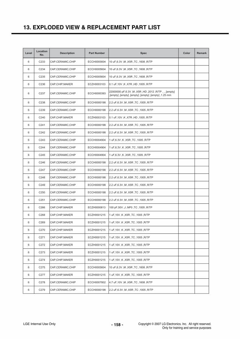
LGE Internal Use Only Copyright © 2007 LG Electronics. Inc. All right reserved. Only for training and service purposes
13. EXPLODED VIEW & REPLACEMENT PART LIST
- 158 -
LevelLocation
No.Description Part Number Spec Color Remark
6 C233 CAP,CERAMIC,CHIP ECCH0005604 10 uF,6.3V ,M ,X5R ,TC ,1608 ,R/TP
6 C234 CAP,CERAMIC,CHIP ECCH0005604 10 uF,6.3V ,M ,X5R ,TC ,1608 ,R/TP
6 C235 CAP,CERAMIC,CHIP ECCH0005604 10 uF,6.3V ,M ,X5R ,TC ,1608 ,R/TP
6 C236 CAP,CHIP,MAKER ECZH0003103 0.1 uF,10V ,K ,X7R ,HD ,1005 ,R/TP
6 C237 CAP,CERAMIC,CHIP ECCH000039322000000 pF,6.3V ,M ,X5R ,HD ,2012 ,R/TP , , ,[empty],[empty] ,[empty] ,[empty] ,[empty] ,[empty] ,1.25 mm
6 C238 CAP,CERAMIC,CHIP ECCH0000198 2.2 uF,6.3V ,M ,X5R ,TC ,1005 ,R/TP
6 C239 CAP,CERAMIC,CHIP ECCH0000198 2.2 uF,6.3V ,M ,X5R ,TC ,1005 ,R/TP
6 C240 CAP,CHIP,MAKER ECZH0003103 0.1 uF,10V ,K ,X7R ,HD ,1005 ,R/TP
6 C241 CAP,CERAMIC,CHIP ECCH0000198 2.2 uF,6.3V ,M ,X5R ,TC ,1005 ,R/TP
6 C242 CAP,CERAMIC,CHIP ECCH0000198 2.2 uF,6.3V ,M ,X5R ,TC ,1005 ,R/TP
6 C243 CAP,CERAMIC,CHIP ECCH0004904 1 uF,6.3V ,K ,X5R ,TC ,1005 ,R/TP
6 C244 CAP,CERAMIC,CHIP ECCH0004904 1 uF,6.3V ,K ,X5R ,TC ,1005 ,R/TP
6 C245 CAP,CERAMIC,CHIP ECCH0004904 1 uF,6.3V ,K ,X5R ,TC ,1005 ,R/TP
6 C246 CAP,CERAMIC,CHIP ECCH0000198 2.2 uF,6.3V ,M ,X5R ,TC ,1005 ,R/TP
6 C247 CAP,CERAMIC,CHIP ECCH0000198 2.2 uF,6.3V ,M ,X5R ,TC ,1005 ,R/TP
6 C248 CAP,CERAMIC,CHIP ECCH0000198 2.2 uF,6.3V ,M ,X5R ,TC ,1005 ,R/TP
6 C249 CAP,CERAMIC,CHIP ECCH0000198 2.2 uF,6.3V ,M ,X5R ,TC ,1005 ,R/TP
6 C250 CAP,CERAMIC,CHIP ECCH0000198 2.2 uF,6.3V ,M ,X5R ,TC ,1005 ,R/TP
6 C251 CAP,CERAMIC,CHIP ECCH0000198 2.2 uF,6.3V ,M ,X5R ,TC ,1005 ,R/TP
6 C266 CAP,CHIP,MAKER ECZH0000813 100 pF,50V ,J ,NP0 ,TC ,1005 ,R/TP
6 C268 CAP,CHIP,MAKER ECZH0001215 1 uF,10V ,K ,X5R ,TC ,1005 ,R/TP
6 C269 CAP,CHIP,MAKER ECZH0001215 1 uF,10V ,K ,X5R ,TC ,1005 ,R/TP
6 C270 CAP,CHIP,MAKER ECZH0001215 1 uF,10V ,K ,X5R ,TC ,1005 ,R/TP
6 C271 CAP,CHIP,MAKER ECZH0001215 1 uF,10V ,K ,X5R ,TC ,1005 ,R/TP
6 C272 CAP,CHIP,MAKER ECZH0001215 1 uF,10V ,K ,X5R ,TC ,1005 ,R/TP
6 C273 CAP,CHIP,MAKER ECZH0001215 1 uF,10V ,K ,X5R ,TC ,1005 ,R/TP
6 C274 CAP,CHIP,MAKER ECZH0001215 1 uF,10V ,K ,X5R ,TC ,1005 ,R/TP
6 C275 CAP,CERAMIC,CHIP ECCH0005604 10 uF,6.3V ,M ,X5R ,TC ,1608 ,R/TP
6 C277 CAP,CHIP,MAKER ECZH0001215 1 uF,10V ,K ,X5R ,TC ,1005 ,R/TP
6 C278 CAP,CERAMIC,CHIP ECCH0007802 4.7 uF,10V ,M ,X5R ,TC ,1608 ,R/TP
6 C279 CAP,CERAMIC,CHIP ECCH0000198 2.2 uF,6.3V ,M ,X5R ,TC ,1005 ,R/TP

LGE Internal Use OnlyCopyright © 2007 LG Electronics. Inc. All right reserved. Only for training and service purposes
13. EXPLODED VIEW & REPLACEMENT PART LIST
- 159 -
LevelLocation
No.Description Part Number Spec Color Remark
6 C280 CAP,CERAMIC,CHIP ECCH0004904 1 uF,6.3V ,K ,X5R ,TC ,1005 ,R/TP
6 C281 CAP,CHIP,MAKER ECZH0001215 1 uF,10V ,K ,X5R ,TC ,1005 ,R/TP
6 C282 CAP,CHIP,MAKER ECZH0003103 0.1 uF,10V ,K ,X7R ,HD ,1005 ,R/TP
6 C283 CAP,CERAMIC,CHIP ECCH0000198 2.2 uF,6.3V ,M ,X5R ,TC ,1005 ,R/TP
6 C285 CAP,CHIP,MAKER ECZH0003103 0.1 uF,10V ,K ,X7R ,HD ,1005 ,R/TP
6 C287 CAP,CERAMIC,CHIP ECCH0000198 2.2 uF,6.3V ,M ,X5R ,TC ,1005 ,R/TP
6 C301 CAP,CHIP,MAKER ECZH0003103 0.1 uF,10V ,K ,X7R ,HD ,1005 ,R/TP
6 C302 CAP,CHIP,MAKER ECZH0000813 100 pF,50V ,J ,NP0 ,TC ,1005 ,R/TP
6 C303 CAP,CERAMIC,CHIP ECCH0000110 10 pF,50V,D,NP0,TC,1005,R/TP
6 C324 CAP,CHIP,MAKER ECZH0000901 24 pF,50V ,J ,NP0 ,TC ,1005 ,R/TP
6 C329 CAP,CHIP,MAKER ECZH0000901 24 pF,50V ,J ,NP0 ,TC ,1005 ,R/TP
6 C330 CAP,CERAMIC,CHIP ECCH0000198 2.2 uF,6.3V ,M ,X5R ,TC ,1005 ,R/TP
6 C333 CAP,CERAMIC,CHIP ECCH0000127 82 pF,50V,J,NP0,TC,1005,R/TP
6 C334 CAP,CERAMIC,CHIP ECCH0000127 82 pF,50V,J,NP0,TC,1005,R/TP
6 C338 CAP,CHIP,MAKER ECZH0003103 0.1 uF,10V ,K ,X7R ,HD ,1005 ,R/TP
6 C339 CAP,CHIP,MAKER ECZH0001215 1 uF,10V ,K ,X5R ,TC ,1005 ,R/TP
6 C340 CAP,CHIP,MAKER ECZH0001215 1 uF,10V ,K ,X5R ,TC ,1005 ,R/TP
6 C341 CAP,CHIP,MAKER ECZH0003103 0.1 uF,10V ,K ,X7R ,HD ,1005 ,R/TP
6 C342 CAP,CHIP,MAKER ECZH0003103 0.1 uF,10V ,K ,X7R ,HD ,1005 ,R/TP
6 C343 CAP,CHIP,MAKER ECZH0001215 1 uF,10V ,K ,X5R ,TC ,1005 ,R/TP
6 C344 CAP,CHIP,MAKER ECZH0001215 1 uF,10V ,K ,X5R ,TC ,1005 ,R/TP
6 C345 CAP,CHIP,MAKER ECZH0001215 1 uF,10V ,K ,X5R ,TC ,1005 ,R/TP
6 C346 CAP,CERAMIC,CHIP ECCH0000112 15 pF,50V,J,NP0,TC,1005,R/TP
6 C349 CAP,CERAMIC,CHIP ECCH0000112 15 pF,50V,J,NP0,TC,1005,R/TP
6 C350 CAP,CHIP,MAKER ECZH0003103 0.1 uF,10V ,K ,X7R ,HD ,1005 ,R/TP
6 C351 CAP,CHIP,MAKER ECZH0001215 1 uF,10V ,K ,X5R ,TC ,1005 ,R/TP
6 C353 CAP,CERAMIC,CHIP ECCH0000117 27 pF,50V,J,NP0,TC,1005,R/TP
6 C354 CAP,CERAMIC,CHIP ECCH0000117 27 pF,50V,J,NP0,TC,1005,R/TP
6 C355 CAP,CHIP,MAKER ECZH0001215 1 uF,10V ,K ,X5R ,TC ,1005 ,R/TP
6 C403 CAP,CERAMIC,CHIP ECCH0000143 1 nF,50V,K,X7R,HD,1005,R/TP
6 C423 CAP,CERAMIC,CHIP ECCH0000151 4.7 nF,25V,K,X7R,HD,1005,R/TP

LGE Internal Use Only Copyright © 2007 LG Electronics. Inc. All right reserved. Only for training and service purposes
13. EXPLODED VIEW & REPLACEMENT PART LIST
- 160 -
LevelLocation
No.Description Part Number Spec Color Remark
6 C437 CAP,CERAMIC,CHIP ECCH0000155 10 nF,16V,K,X7R,HD,1005,R/TP
6 C440 CAP,CERAMIC,CHIP ECCH0000112 15 pF,50V,J,NP0,TC,1005,R/TP
6 C441 CAP,CHIP,MAKER ECZH0003103 0.1 uF,10V ,K ,X7R ,HD ,1005 ,R/TP
6 C442 CAP,CERAMIC,CHIP ECCH0000198 2.2 uF,6.3V ,M ,X5R ,TC ,1005 ,R/TP
6 C448 CAP,CERAMIC,CHIP ECCH0000112 15 pF,50V,J,NP0,TC,1005,R/TP
6 C449 CAP,CERAMIC,CHIP ECCH0000112 15 pF,50V,J,NP0,TC,1005,R/TP
6 C450 CAP,CERAMIC,CHIP ECCH0000163 47 nF,10V,K,X5R,HD,1005,R/TP
6 C451 CAP,CHIP,MAKER ECZH0001216 220 nF,10V ,K ,X5R ,TC ,1005 ,R/TP
6 C452 CAP,CERAMIC,CHIP ECCH0000143 1 nF,50V,K,X7R,HD,1005,R/TP
6 C453 CAP,CHIP,MAKER ECZH0003103 0.1 uF,10V ,K ,X7R ,HD ,1005 ,R/TP
6 C454 CAP,CERAMIC,CHIP ECCH0000143 1 nF,50V,K,X7R,HD,1005,R/TP
6 C455 CAP,CHIP,MAKER ECZH0001126 820 pF,50V ,K ,X7R ,HD ,1005 ,R/TP
6 C456 CAP,CHIP,MAKER ECZH0001126 820 pF,50V ,K ,X7R ,HD ,1005 ,R/TP
6 C457 CAP,CERAMIC,CHIP ECCH0000112 15 pF,50V,J,NP0,TC,1005,R/TP
6 C458 CAP,CERAMIC,CHIP ECCH0000112 15 pF,50V,J,NP0,TC,1005,R/TP
6 C460 CAP,CERAMIC,CHIP ECCH0000112 15 pF,50V,J,NP0,TC,1005,R/TP
6 C461 CAP,CHIP,MAKER ECZH0003103 0.1 uF,10V ,K ,X7R ,HD ,1005 ,R/TP
6 C462 CAP,CHIP,MAKER ECZH0003103 0.1 uF,10V ,K ,X7R ,HD ,1005 ,R/TP
6 C463 CAP,CERAMIC,CHIP ECCH0000155 10 nF,16V,K,X7R,HD,1005,R/TP
6 C464 CAP,CERAMIC,CHIP ECCH0000198 2.2 uF,6.3V ,M ,X5R ,TC ,1005 ,R/TP
6 C465 CAP,CERAMIC,CHIP ECCH0000198 2.2 uF,6.3V ,M ,X5R ,TC ,1005 ,R/TP
6 CN303CONNECTOR,BOARD TOBOARD
ENBY0016701 20 PIN,0.4 mm,STRAIGHT ,AU ,0.9 STACKING,MALE
6 CN304CONNECTOR,BOARD TOBOARD
ENBY0023601 54 PIN,0.4 mm,ETC , ,H=0.9, Header
6 D201 DIODE,SWITCHING EDSY0009901 ESC ,80 V,300 A,R/TP ,1.6*0.8*0.6(t)
6 D202 DIODE,SWITCHING EDSY0009901 ESC ,80 V,300 A,R/TP ,1.6*0.8*0.6(t)
6 FB201 FILTER,BEAD,CHIP SFBH0001003 220 ohm,2012 ,
6 FB202 FILTER,BEAD,CHIP SFBH0001003 220 ohm,2012 ,
6 FL304 FILTER,EMI/POWER SFEY0015101 SMD ,Pb-free_8ch_TVS_EMI_ESD ,; ,Filter,LCR
6 FL305 FILTER,EMI/POWER SFEY0015101 SMD ,Pb-free_8ch_TVS_EMI_ESD ,; ,Filter,LCR
6 FL402 FILTER,DIELECTRIC SFDY00026012450 MHz,2.0*1.25*1.0 ,SMD ,2400M~2500M, IL 3.8,8pin, U-B, 34.2_j95, BT (CSR BC41B143A) ,; ,BPF ,2450,100 ,SMD ,R/TP

LGE Internal Use OnlyCopyright © 2007 LG Electronics. Inc. All right reserved. Only for training and service purposes
13. EXPLODED VIEW & REPLACEMENT PART LIST
- 161 -
LevelLocation
No.Description Part Number Spec Color Remark
6 L201 INDUCTOR,SMD,POWER ELCP0006703 10 uH,M ,3.2*2.6*1.0 ,R/TP ,
6 L204 INDUCTOR,CHIP ELCH0005009 100 nH,J ,1005 ,R/TP ,
6 L205 INDUCTOR,CHIP ELCH0005009 100 nH,J ,1005 ,R/TP ,
6 L206 INDUCTOR,SMD,POWER ELCP0005104 10 uH,M ,3.8*3.8*1.8 ,R/TP ,power inductor/ 850mA
6 L207 INDUCTOR,CHIP ELCH0005019 68 nH,J ,1005 ,R/TP ,
6 L208 INDUCTOR,CHIP ELCH0005019 68 nH,J ,1005 ,R/TP ,
6 L301 INDUCTOR,CHIP ELCH0010402 270 nH,M ,1005 ,R/TP ,CHIP
6 L306 RES,CHIP,MAKER ERHZ0000490 51 ohm,1/16W ,J ,1005 ,R/TP
6 L307 INDUCTOR,CHIP ELCH0005009 100 nH,J ,1005 ,R/TP ,
6 L308 RES,CHIP,MAKER ERHZ0000490 51 ohm,1/16W ,J ,1005 ,R/TP
6 L309 INDUCTOR,CHIP ELCH0005009 100 nH,J ,1005 ,R/TP ,
6 L310 INDUCTOR,CHIP ELCH0005009 100 nH,J ,1005 ,R/TP ,
6 L311 INDUCTOR,CHIP ELCH0005009 100 nH,J ,1005 ,R/TP ,
6 L406 INDUCTOR,CHIP ELCH0005006 33 nH,J ,1005 ,R/TP ,
6 L407 INDUCTOR,CHIP ELCH0003823 470 nH,K ,1608 ,R/TP ,chip coil,PBFREE
6 L408 INDUCTOR,CHIP ELCH0004730 33 nH,J ,1005 ,R/TP ,
6 M401 MODULE,ETC SMZY0015801 84 Ball 0.5pitch, BGA , Bluetooth+FM (6.0*6.0*1.0)
6 Q201 TR,BJT,NPN EQBN0017601 VMT3 ,0.15 W,R/TP ,
6 Q202 TR,BJT,NPN EQBN0017601 VMT3 ,0.15 W,R/TP ,
6 Q301 TR,BJT,NPN EQBN0017601 VMT3 ,0.15 W,R/TP ,
6 R102 RES,CHIP ERHY0000166 390 Kohm,1/16W ,F ,1005 ,R/TP
6 R104 RES,CHIP,MAKER ERHZ0000204 100 Kohm,1/16W ,F ,1005 ,R/TP
6 R105 RES,CHIP,MAKER ERHZ0000405 10 Kohm,1/16W ,J ,1005 ,R/TP
6 R106 RES,CHIP,MAKER ERHZ0000267 3300 ohm,1/16W ,F ,1005 ,R/TP
6 R110 RES,CHIP,MAKER ERHZ0000404 1 Kohm,1/16W ,J ,1005 ,R/TP
6 R111 RES,CHIP,MAKER ERHZ0000405 10 Kohm,1/16W ,J ,1005 ,R/TP
6 R112 RES,CHIP,MAKER ERHZ0000444 22 Kohm,1/16W ,J ,1005 ,R/TP
6 R113 RES,CHIP,MAKER ERHZ0000405 10 Kohm,1/16W ,J ,1005 ,R/TP
6 R114 RES,CHIP,MAKER ERHZ0000505 680 ohm,1/16W ,J ,1005 ,R/TP
6 R115 RES,CHIP,MAKER ERHZ0000505 680 ohm,1/16W ,J ,1005 ,R/TP
6 R116 RES,CHIP,MAKER ERHZ0000505 680 ohm,1/16W ,J ,1005 ,R/TP

LGE Internal Use Only Copyright © 2007 LG Electronics. Inc. All right reserved. Only for training and service purposes
13. EXPLODED VIEW & REPLACEMENT PART LIST
- 162 -
LevelLocation
No.Description Part Number Spec Color Remark
6 R117 RES,CHIP,MAKER ERHZ0000505 680 ohm,1/16W ,J ,1005 ,R/TP
6 R118 RES,CHIP,MAKER ERHZ0000505 680 ohm,1/16W ,J ,1005 ,R/TP
6 R119 RES,CHIP,MAKER ERHZ0000505 680 ohm,1/16W ,J ,1005 ,R/TP
6 R120 RES,CHIP,MAKER ERHZ0000505 680 ohm,1/16W ,J ,1005 ,R/TP
6 R121 RES,CHIP,MAKER ERHZ0000505 680 ohm,1/16W ,J ,1005 ,R/TP
6 R122 RES,CHIP,MAKER ERHZ0000505 680 ohm,1/16W ,J ,1005 ,R/TP
6 R124 RES,CHIP,MAKER ERHZ0000319 8200 ohm,1/16W ,F ,1005 ,R/TP
6 R125 RES,CHIP,MAKER ERHZ0000319 8200 ohm,1/16W ,F ,1005 ,R/TP
6 R201 RES,CHIP,MAKER ERHZ0000454 27 Kohm,1/16W ,J ,1005 ,R/TP
6 R206 RES,CHIP,MAKER ERHZ0000485 4700 ohm,1/16W ,J ,1005 ,R/TP
6 R207 RES,CHIP,MAKER ERHZ0000485 4700 ohm,1/16W ,J ,1005 ,R/TP
6 R208 RES,CHIP,MAKER ERHZ0000485 4700 ohm,1/16W ,J ,1005 ,R/TP
6 R210 RES,CHIP,MAKER ERHZ0000485 4700 ohm,1/16W ,J ,1005 ,R/TP
6 R211 RES,CHIP,MAKER ERHZ0000485 4700 ohm,1/16W ,J ,1005 ,R/TP
6 R212 RES,CHIP,MAKER ERHZ0000204 100 Kohm,1/16W ,F ,1005 ,R/TP
6 R223 RES,CHIP,MAKER ERHZ0000406 100 Kohm,1/16W ,J ,1005 ,R/TP
6 R224 RES,CHIP,MAKER ERHZ0000406 100 Kohm,1/16W ,J ,1005 ,R/TP
6 R225 RES,CHIP,MAKER ERHZ0000434 1 ohm,1/16W ,J ,1005 ,R/TP
6 R228 RES,CHIP,MAKER ERHZ0000406 100 Kohm,1/16W ,J ,1005 ,R/TP
6 R229 RES,CHIP,MAKER ERHZ0000404 1 Kohm,1/16W ,J ,1005 ,R/TP
6 R230 RES,CHIP,MAKER ERHZ0000243 2200 ohm,1/16W ,F ,1005 ,R/TP
6 R231 RES,CHIP,MAKER ERHZ0000279 39 Kohm,1/16W ,F ,1005 ,R/TP
6 R232 RES,CHIP ERHY0008402 160 Kohm,1/16W ,F ,1005 ,R/TP
6 R233 RES,CHIP,MAKER ERHZ0000406 100 Kohm,1/16W ,J ,1005 ,R/TP
6 R235 RES,CHIP,MAKER ERHZ0000405 10 Kohm,1/16W ,J ,1005 ,R/TP
6 R236 RES,CHIP,MAKER ERHZ0000406 100 Kohm,1/16W ,J ,1005 ,R/TP
6 R237 RES,CHIP,MAKER ERHZ0000406 100 Kohm,1/16W ,J ,1005 ,R/TP
6 R239 RES,CHIP,MAKER ERHZ0000406 100 Kohm,1/16W ,J ,1005 ,R/TP
6 R241 RES,CHIP,MAKER ERHZ0000406 100 Kohm,1/16W ,J ,1005 ,R/TP
6 R244 RES,CHIP,MAKER ERHZ0000405 10 Kohm,1/16W ,J ,1005 ,R/TP
6 R248 RES,CHIP,MAKER ERHZ0000358 280 Kohm,1/16W ,F ,1005 ,R/TP

LGE Internal Use OnlyCopyright © 2007 LG Electronics. Inc. All right reserved. Only for training and service purposes
13. EXPLODED VIEW & REPLACEMENT PART LIST
- 163 -
LevelLocation
No.Description Part Number Spec Color Remark
6 R249 RES,CHIP,MAKER ERHZ0000516 820 Kohm,1/16W ,J ,1005 ,R/TP
6 R252 RES,CHIP ERHY0008402 160 Kohm,1/16W ,F ,1005 ,R/TP
6 R254 RES,CHIP,MAKER ERHZ0000213 120 Kohm,1/16W ,F ,1005 ,R/TP
6 R303 RES,CHIP,MAKER ERHZ0000407 1000 Kohm,1/16W ,J ,1005 ,R/TP
6 R305 RES,CHIP,MAKER ERHZ0000467 330 Kohm,1/16W ,J ,1005 ,R/TP
6 R321 RES,CHIP,MAKER ERHZ0000405 10 Kohm,1/16W ,J ,1005 ,R/TP
6 R325 RES,CHIP,MAKER ERHZ0000406 100 Kohm,1/16W ,J ,1005 ,R/TP
6 R335 RES,CHIP ERHY0003301 100 ohm,1/16W ,J ,1005 ,R/TP
6 R337 RES,CHIP,MAKER ERHZ0000402 10 ohm,1/16W ,J ,1005 ,R/TP
6 R338 RES,CHIP,MAKER ERHZ0000319 8200 ohm,1/16W ,F ,1005 ,R/TP
6 R339 RES,CHIP,MAKER ERHZ0000319 8200 ohm,1/16W ,F ,1005 ,R/TP
6 R340 RES,CHIP,MAKER ERHZ0000405 10 Kohm,1/16W ,J ,1005 ,R/TP
6 R341 RES,CHIP,MAKER ERHZ0000485 4700 ohm,1/16W ,J ,1005 ,R/TP
6 R342 RES,CHIP,MAKER ERHZ0000405 10 Kohm,1/16W ,J ,1005 ,R/TP
6 R343 RES,CHIP,MAKER ERHZ0000405 10 Kohm,1/16W ,J ,1005 ,R/TP
6 R344 RES,CHIP ERHY0003301 100 ohm,1/16W ,J ,1005 ,R/TP
6 R415 RES,CHIP,MAKER ERHZ0000434 1 ohm,1/16W ,J ,1005 ,R/TP
6 R417 RES,CHIP,MAKER ERHZ0000434 1 ohm,1/16W ,J ,1005 ,R/TP
6 R419 RES,CHIP,MAKER ERHZ0000401 0 ohm,1/16W ,J ,1005 ,R/TP
6 R420 RES,CHIP,MAKER ERHZ0000496 560 ohm,1/16W ,J ,1005 ,R/TP
6 R421 RES,CHIP,MAKER ERHZ0000456 2.2 ohm,1/16W ,J ,1005 ,R/TP
6 R422 RES,CHIP,MAKER ERHZ0000287 47 Kohm,1/16W ,F ,1005 ,R/TP
6 SPFY00 PCB,MAIN SPFY0163101 FR-4 ,0.8 mm,STAGGERED-10 , ,; , , , , , , , , ,
6 U101 IC EUSY0335802FBGA ,107 PIN,ETC ,FULLY 1.8V 1G(128Mx8)NAND+512M(DDR/8Mx4x16) SDRAM ,; ,IC,MCP
6 U102 IC EUSY0322801 BGA ,293 PIN,R/TP ,Multimedia Extension EDGE BB
6 U202 IC EUSY0340301uMLP ,10 PIN,R/TP ,typ Rdson 0.4ohm, 1.4X1.8 ,;,IC,Analog Switch
6 U203 IC EUSY0323901 BGA PG-WFSGA ,121 PIN,R/TP ,SMPOWER3
6 U205 IC EUSY0254701DFN 3*3*0.9 ,10 PIN,R/TP ,Charger IC, I Max 1A, WallAdaptor/USB Charger
6 U206 IC EUSY0337001 TDFN33 ,12 PIN,R/TP ,3x3x1.0
6 U207 IC EUSY0294801 SON1612-6 ,6 PIN,R/TP ,3.1V 150mA LDO Pb-Free

LGE Internal Use Only Copyright © 2007 LG Electronics. Inc. All right reserved. Only for training and service purposes
13. EXPLODED VIEW & REPLACEMENT PART LIST
- 164 -
LevelLocation
No.Description Part Number Spec Color Remark
6 U208 IC EUSY0102802 Micropak ,8 PIN,R/TP ,Daul 2 input AND gate,
6 U210 IC EUSY0238304 QFN ,28 PIN,R/TP ,Charge pump400mA,2LDO,200mA
6 U301 IC EUSY0250501SC70 ,5 PIN,R/TP ,Comparator, pin compatible toEUSY0077701
6 U306 IC EUSY0342402DFN ,8 PIN,R/TP ,Levelshifter,autodirection ,; ,IC,BusController
6 U307 IC EUSY0321201 BGA ,64 PIN,R/TP ,6*6 ISP
6 U401 IC EUSY0279801 SC70 ,6 PIN,R/TP ,Dual Buffer, Pb Free
6 VA303 VARISTOR SEVY0003601 5.6 V, ,SMD ,100pF, 1005
6 VA304 VARISTOR SEVY0003601 5.6 V, ,SMD ,100pF, 1005
6 VA305 VARISTOR SEVY0003601 5.6 V, ,SMD ,100pF, 1005
6 VA306 VARISTOR SEVY0003601 5.6 V, ,SMD ,100pF, 1005
6 VA307 VARISTOR SEVY0003601 5.6 V, ,SMD ,100pF, 1005
6 VA308 VARISTOR SEVY0003601 5.6 V, ,SMD ,100pF, 1005
6 VA309 VARISTOR SEVY0003601 5.6 V, ,SMD ,100pF, 1005
6 VA310 VARISTOR SEVY0003601 5.6 V, ,SMD ,100pF, 1005
6 VA311 VARISTOR SEVY0003601 5.6 V, ,SMD ,100pF, 1005
6 VA312 VARISTOR SEVY0003601 5.6 V, ,SMD ,100pF, 1005
6 VA313 VARISTOR SEVY0003601 5.6 V, ,SMD ,100pF, 1005
6 VA314 VARISTOR SEVY0003601 5.6 V, ,SMD ,100pF, 1005
6 VA315 VARISTOR SEVY0003601 5.6 V, ,SMD ,100pF, 1005
6 X101 X-TAL EXXY001870132.768 KHz,20 PPM,12.5 pF,70 Kohm,SMD ,3.2*1.5*0.9,
3 SNGF00 ANTENNA,GSM,FIXED SNGF00323013.0 ,-2.0 dBd,, ,internal, GSM900/1800/1900 ,; ,TRIPLE ,-2.0 ,50 ,3.0
77

- 165 - LGE Internal Use OnlyCopyright © 2007 LG Electronics. Inc. All right reserved. Only for training and service purposes
LevelLocation
No.Description Part Number Spec Color Remark
3 SBPL00 BATTERY PACK,LI-ION SBPL0085703
3.7 V,800 mAh,1 CELL,PRISMATIC ,CMW PJT BATT,Innerpack, Europe Label, Pb-Free ,; ,3.7 ,800 ,0.2C,PRISMATIC ,43x34x46 , ,ALLTEL SILVER ,Innerpack,CMW Slide & Folder
AIRY BLUE
3 SGDY00 DATA CABLE SGDY0010904; ,[empty] ,[empty] ,[empty] ,18 ,BLACK ,6.2mm PlugDatacable ,[empty]
3 SGEY00EAR PHONE/EAR MIKESET
SGEY0005558
;,RMS 20mW(0.56V,RMS),16OHM,116dB,1KHZ,3mW,96dB100HZ,116dB1KHZ,[empty],BLACK,EARPHONE HOUSING:SILVER,18P MMICONNECTOR,,Earphone,Stereo
3 SSAD00 ADAPTOR,AC-DC SSAD0024901100-240V ,5060 Hz,5.1 V,.7 A,CB/GOST ,AC-DCADAPTOR ,; ,100Vac~350Vac ,5.1V (+0.15, -0.2),700mA ,5060 , ,WALL 2P ,I/O CONNECTOR ,
ADAPTOR,AC-DC SSAD0024902100-240V ,5060 Hz,5.1 V,.7 A,CB/GOST ,AC-DCADAPTOR ,; ,100Vac~350Vac ,5.1V (+0.15,-0.2) ,700mA,5060 , ,WALL 2P ,I/O CONNECTOR ,
12.3 Accessory Note: This Chapter is used for reference, Part orderis ordered by SBOM standard on GCSC
13. EXPLODED VIEW & REPLACEMENT PART LIST

Note

Note