man - can pic - uk - 5
TRANSCRIPT

, GPC®, grifo ®, are trade marks of grifo ®
TECHNICAL MANUAL
CAN PICCAN - grifo ® Mini Module PIC
CAN PIC Rel. 5.00 Edition 07 February 2006
Via dell' Artigiano, 8/640016 San Giorgio di Piano(Bologna) ITALYE-mail: [email protected]
http://www.grifo.it http://www.grifo.comTel. +39 051 892.052 (a.r.) FAX: +39 051 893.661
grifo ®
ITALIAN TECHNOLOGY
Standard container with 28 pins male socket, dual in line, 100 mils pitch, 600 mils width;very small dimension: 43 x 25 x 15 mm; single power supply voltage required in the widerange from 5.0 Vdc (the current consumption can change according with moduleconnections); availability of power saving setting as Idle Mode and Power Down Mode;Microchip PIC18F4680 microcontroller with working frequency 40 MHz; 64 KBytesFLASH for code, 3328 Bytes SRAM for data, 1KBytes EEPROM for data; 2 analogcomparators with different input and output configurations options that allow to createeasily bipolar A/D conversion; 10 channels multiplexed A/D converter, resolution 10 bitsand 20 µsec conversion time; 32 Interrupt sources; 4 Timers Counters, up to 16 bits;2 peripherals featuring PWM , compare, capture, etc.; up to 24 digital I/O lines availableon connector. Some of these lines have multiple functions; one hardware serialcommunication line with programmable physical protocol (Baud Rate up to 115200Baud, 8 or 9 data bits, 1 or 2 stop bit), RS 232 buffered or at TTL level; one CANdifferential serial line completely compatible with CAN 2.0 specifications part A and B;In Circuit Debugger interface for in-circuit remote debugging with MPLAB ® IDE ; I 2CBUS controller, completely software configurable; SPI interface programmable forsyncronous, high speed communications; Reset circuitery; programmable Watch Dogfrom 41 ms up to 131 s; one configuration dip switch; one Real Time Clock for long andaccurate timing, active even in low power modes, capable to manage date and time andto generate periodic interrupts; 240 bytes of SRAM for configuration parameters; RTCand SRAM backed with on-board Lithium battery; 2 status LEDs managed by softwarethrough two digital I/O lines; internal FLASH and EEPROM can be managed throughISP (In System Programming); wide range of Software Development tools used todevelop the user application program, as: Assembler; C compilers (HI-TECH PICC);BASIC Compilers (PIC BASIC PRO, mikroBasic); PASCAL Compilers (mikroPascal);etc.; long list of Demo Programs and use examples supplied under source form, dulyremarked, and executable form for the available development tools.

DOCUMENTATION COPYRIGHT BY grifo ® , ALL RIGHTS RESERVED
No part of this document may be reproduced, transmitted, transcribed, stored in aretrieval system, or translated into any language or computer language, in any form orby any means, either electronic, mechanical, magnetic, optical, chemical, manual, orotherwise, without the prior written consent of grifo ®.
IMPORTANT
Although all the information contained herein have been carefully verified, grifo ®
assumes no responsability for errors that might appear in this document, or for damageto things or persons resulting from technical errors, omission and improper use of thismanual and of the related software and hardware.
grifo ® reserves the right to change the contents and form of this document, as well asthe features and specification of its products at any time, without prior notice, to obtainalways the best product.For specific informations on the components mounted on the card, please refer to theData Book of the builder or second sources.
SYMBOLS DESCRIPTION
In the manual could appear the following symbols:
Attention: Generic danger
Attention: High voltage
Attention: ESD sensitive device
Trade Marks
, GPC®, grifo ® : are trade marks of grifo ®.Other Product and Company names listed, are trade marks of their respective companies.

ITALIAN TECHNOLOGY grifo ®
Page I CAN PIC Rel. 5.00
GENERAL INDEX
INTRODUCTION ........................................................................................................................ 1
CARD VERSION ......................................................................................................................... 3
GENERAL INFORMATION ...................................................................................................... 4 DIGITAL I/O LINES............................................................................................................... 6 SERIAL COMMUNICATION ............................................................................................... 6 CLOCK .................................................................................................................................... 6 MEMORY DEVICES.............................................................................................................. 8 I2C BUS INTERFACE............................................................................................................. 8 SPI INTERFACE..................................................................................................................... 8 CAN INTERFACE .................................................................................................................. 9 DIP SWITCH ........................................................................................................................... 9 A/D CONVERTERS .............................................................................................................. 10 ANALOG COMPARATORS................................................................................................ 10 TIMER COUNTER AND PWM .......................................................................................... 10 WATCH DOG ........................................................................................................................ 10 REAL TIME CLOCK ...........................................................................................................10
TECHNICAL FEATURES ........................................................................................................ 12 GENERAL FEATURES........................................................................................................ 12 PHYSICAL FEATURES....................................................................................................... 13 ELECTRIC FEATURES ...................................................................................................... 13
INSTALLATION ........................................................................................................................ 14 VISUAL SIGNALATIONS ................................................................................................... 14 CONNECTIONS ................................................................................................................... 14 CN1 - EXTERNAL POWER SUPPLY CONNECTOR ................................................ 14 MINI MODULE CONFIGURATION ................................................................................. 16 SERIAL COMMUNICATION SELECTION..................................................................... 18 CONNECTOR SIGNALS INTERFACEMENT ................................................................ 20 POWER SUPPLY .................................................................................................................. 20 INTERRUPTS ....................................................................................................................... 21 IN CIRCUIT DEBUGGER................................................................................................... 21
SUPPORT CARDS ..................................................................................................................... 22 USE WITH GMB HR84 MODULE..................................................................................... 22 USE WITH CAN GMT MODULE ...................................................................................... 24
HOW TO START ....................................................................................................................... 26 PROGRAMMING WITH MICROCHIP MP LAB ® ICD 2 AND grifo ® GMM PIC-PR 28 PROGRAMMING WITH MICROCHIP grifo ® MP PIK+ AND grifo ® GMM PIC-PR 32 RICOMPILATION WITH PIC BASIC PRO..................................................................... 35 RICOMPILATION WITH MIKROBASIC........................................................................ 36

grifo ® ITALIAN TECHNOLOGY
Page II CAN PIC Rel. 5.00
RICOMPILATION WITH MIKROPASCAL. ................................................................... 37 RICOMPILATION WITH HI TECH PICC18 + MP LAB ® IDE. .................................... 38
SOFTWARE DESCRIPTION ................................................................................................... 40
PERIPHERAL DEVICES SOFTWARE DESCRIPTION ..................................................... 42 ACTIVITY LEDS .................................................................................................................. 42 DIP SWITCH ......................................................................................................................... 42 BACKED SRAM + SERIAL RTC ....................................................................................... 43 CPU INTERNAL PERIPHERALS...................................................................................... 43
BIBLIOGRAPHY....................................................................................................................... 44
APPENDIX A: DATA SHEET................................................................................................. A-1 PIC18F4680 ............................................................................................................................ A-1 PCF8583 ................................................................................................................................. A-2
APPENDIX B: CAN GMT ELECTRIC DIAGRAM ........................................................... B-1
APPENDIX C: ALPHABETICAL INDEX ............................................................................ C-1
ITALIAN TECHNOLOGY grifo ®
Page III CAN PIC Rel. 5.00
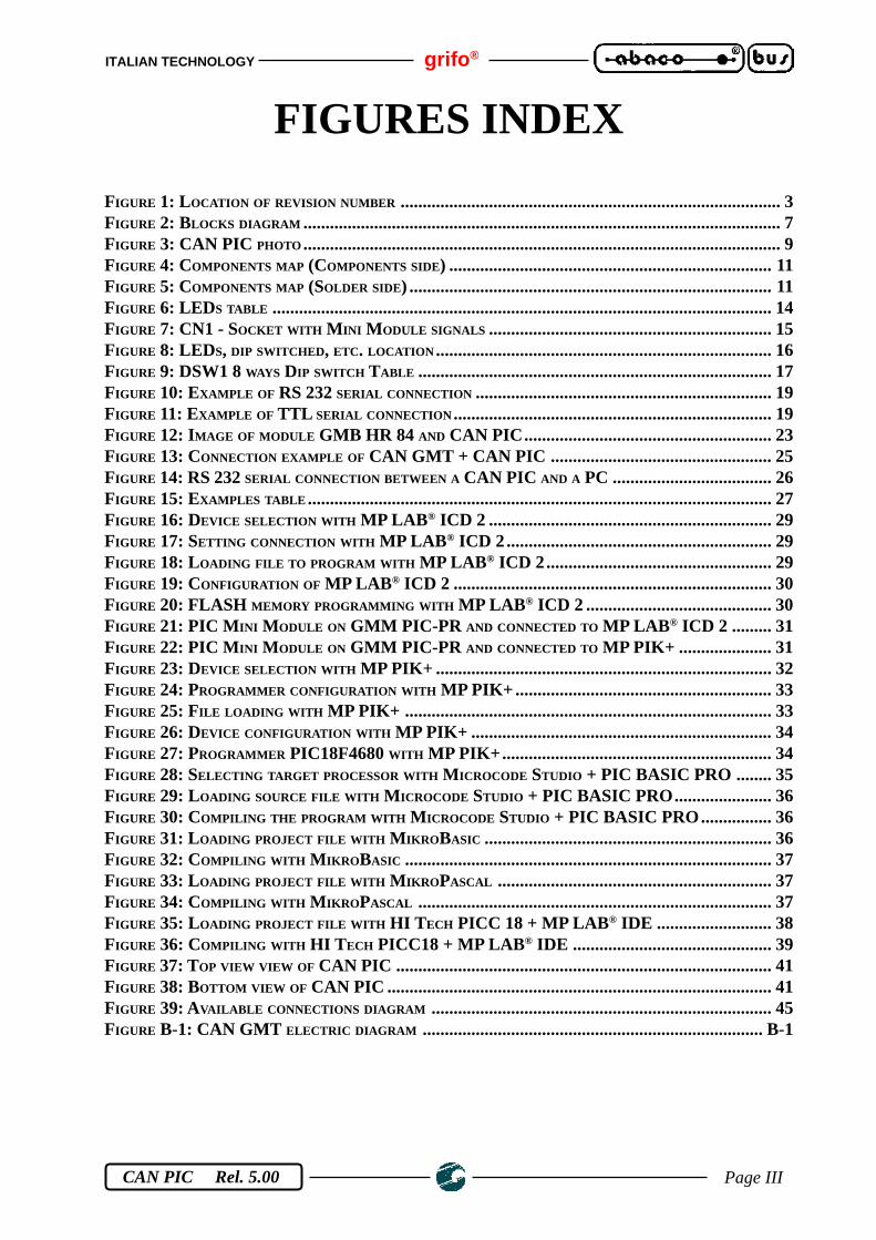
FIGURES INDEX
FIGURE 1: LOCATION OF REVISION NUMBER ...................................................................................... 3FIGURE 2: BLOCKS DIAGRAM ............................................................................................................ 7FIGURE 3: CAN PIC PHOTO ............................................................................................................ 9FIGURE 4: COMPONENTS MAP (COMPONENTS SIDE) ......................................................................... 11FIGURE 5: COMPONENTS MAP (SOLDER SIDE) .................................................................................. 11FIGURE 6: LEDS TABLE ................................................................................................................. 14FIGURE 7: CN1 - SOCKET WITH MINI MODULE SIGNALS ................................................................ 15FIGURE 8: LEDS, DIP SWITCHED , ETC. LOCATION ............................................................................ 16FIGURE 9: DSW1 8 WAYS DIP SWITCH TABLE ................................................................................ 17FIGURE 10: EXAMPLE OF RS 232 SERIAL CONNECTION ................................................................... 19FIGURE 11: EXAMPLE OF TTL SERIAL CONNECTION ........................................................................ 19FIGURE 12: IMAGE OF MODULE GMB HR 84 AND CAN PIC........................................................ 23FIGURE 13: CONNECTION EXAMPLE OF CAN GMT + CAN PIC .................................................. 25FIGURE 14: RS 232 SERIAL CONNECTION BETWEEN A CAN PIC AND A PC .................................... 26FIGURE 15: EXAMPLES TABLE ......................................................................................................... 27FIGURE 16: DEVICE SELECTION WITH MP LAB ® ICD 2 ................................................................ 29FIGURE 17: SETTING CONNECTION WITH MP LAB ® ICD 2............................................................ 29FIGURE 18: LOADING FILE TO PROGRAM WITH MP LAB ® ICD 2................................................... 29FIGURE 19: CONFIGURATION OF MP LAB ® ICD 2 ........................................................................ 30FIGURE 20: FLASH MEMORY PROGRAMMING WITH MP LAB ® ICD 2 .......................................... 30FIGURE 21: PIC MINI MODULE ON GMM PIC-PR AND CONNECTED TO MP LAB ® ICD 2 ......... 31FIGURE 22: PIC MINI MODULE ON GMM PIC-PR AND CONNECTED TO MP PIK+ ..................... 31FIGURE 23: DEVICE SELECTION WITH MP PIK+ ............................................................................ 32FIGURE 24: PROGRAMMER CONFIGURATION WITH MP PIK+ .......................................................... 33FIGURE 25: FILE LOADING WITH MP PIK+ ................................................................................... 33FIGURE 26: DEVICE CONFIGURATION WITH MP PIK+ .................................................................... 34FIGURE 27: PROGRAMMER PIC18F4680 WITH MP PIK+............................................................. 34FIGURE 28: SELECTING TARGET PROCESSOR WITH MICROCODE STUDIO + PIC BASIC PRO ........ 35FIGURE 29: LOADING SOURCE FILE WITH MICROCODE STUDIO + PIC BASIC PRO...................... 36FIGURE 30: COMPILING THE PROGRAM WITH MICROCODE STUDIO + PIC BASIC PRO................ 36FIGURE 31: LOADING PROJECT FILE WITH MIKRO BASIC ................................................................. 36FIGURE 32: COMPILING WITH MIKRO BASIC ................................................................................... 37FIGURE 33: LOADING PROJECT FILE WITH MIKRO PASCAL .............................................................. 37FIGURE 34: COMPILING WITH MIKRO PASCAL ................................................................................ 37FIGURE 35: LOADING PROJECT FILE WITH HI T ECH PICC 18 + MP LAB® IDE .......................... 38FIGURE 36: COMPILING WITH HI T ECH PICC18 + MP LAB® IDE ............................................. 39FIGURE 37: TOP VIEW VIEW OF CAN PIC ..................................................................................... 41FIGURE 38: BOTTOM VIEW OF CAN PIC ....................................................................................... 41FIGURE 39: AVAILABLE CONNECTIONS DIAGRAM ............................................................................. 45FIGURE B-1: CAN GMT ELECTRIC DIAGRAM ............................................................................. B-1

grifo ® ITALIAN TECHNOLOGY
Page IV CAN PIC Rel. 5.00

ITALIAN TECHNOLOGY grifo ®
Page 1 CAN PIC Rel. 5.00
INTRODUCTION
The use of these devices has turned - IN EXCLUSIVE WAY - to specialized personnel.This device is not a safe component as defined in directive 98-37/CE.
Pins of Mini Module are not provided with any kind of ESD protection. They are connected directlyto their respective pins of microcontroller. Mini Module is affected by electrostatic discharges.Personnel who handles Mini Modules is invited to take all necessary precautions to avoid possibledamages caused by electrostatic discharges.
The purpose of this handbook is to give the necessary information to the cognizant and sure use ofthe products. They are the result of a continual and systematic elaboration of data and technical testssaved and validated from the manufacturer, related to the inside modes of certainty and quality ofthe information.
The reported data are destined- IN EXCLUSIVE WAY- to specialized users, that can interact withthe devices in safety conditions for the persons, for the machine and for the enviroment, impersonatingan elementary diagnostic of breakdowns and of malfunction conditions by performing simplefunctional verify operations , in the height respect of the actual safety and health norms.
The informations for the installation, the assemblage, the dismantlement, the handling, the adjustment,the reparation and the contingent accessories, devices etc. installation are destined - and thenexecutable - always and in exclusive way from specialized warned and educated personnel, ordirectly from the TECHNICAL AUTHORIZED ASSISTANCE, in the height respect of themanufacturer recommendations and the actual safety and health norms.
The devices can't be used outside a box. The user must always insert the cards in a container thatrispect the actual safety normative. The protection of this container is not threshold to the onlyatmospheric agents, but specially to mechanic, electric, magnetic, etc. ones.
To be on good terms with the products, is necessary guarantee legibility and conservation of themanual, also for future references. In case of deterioration or more easily for technical updates,consult the AUTHORIZED TECHNICAL ASSISTANCE directly.

grifo ® ITALIAN TECHNOLOGY
Page 2 CAN PIC Rel. 5.00
To prevent problems during card utilization, it is a good practice to read carefully all the informationsof this manual. After this reading, the user can use the general index and the alphabetical index,respectly at the begining and at the end of the manual, to find information in a faster and more easyway.

ITALIAN TECHNOLOGY grifo ®
Page 3 CAN PIC Rel. 5.00
CARD VERSION
This handbook make reference to card CAN PIC with printed circuit version 101104.The validity of the information contained in this manual is subordinated to the printed circuit revisionnumber and so the user must always check the correspondance.The printed circuit revision number is always printed in several positions of the circuit and followingfigure shows the easiest to access.
PRINTED CIRCUIT REVISION NUMBER
FIGURE 1: LOCATION OF REVISION NUMBER

grifo ® ITALIAN TECHNOLOGY
Page 4 CAN PIC Rel. 5.00
GENERAL INFORMATION
CAN PIC (CAN - grifo ® Mini Module PIC) is a module based on microcontroller MicrochipPIC18F4680, a powerful and complete system on a chip provided with CPU, integrated memory(both for data and code), a watch dog, many digital I/O lines, 4 timers counters, peripheralsfeaturing capture and compare capability, one asynchronous serial line, one CAN serial line, one I 2CBUS synchronous seria line, 2 comparators for analog signals, etc.In module's very small area, are already mounted the components that exploit microcontrollers'sperformance and that allow each functionality mode like a reset generator circuitery.Possible applications of CAN PIC Mini Modules are several.For example, native CAN application, that is car automation (lights turning ON/OFF, heating andcooling systems control, supervision of electric devices, anti-teft and acces control systems,functionality checks, etc.). Also, connection on CAN networks with your own protocols or withstandard protocols (like CANopen, DeviceNet, SDS, CAN Kingdom etc.).We remark the employ as smart intelligent nodes with local functionalities as PID algorithms forcontrolling temperatures, motors, valves, etc. or as decentralized systems as robots, automation ofproduction line machines, big factory automations.Finally, teleacquisition and telecontrol on medium and low distances, conversion between CANand asynchronous serial line or I 2C BUS line and home automation (lights turning ON/OFF,heating and cooling systems control, supervision of electric devices, security and acces controlsystems).It is really important the Didactics use in fact CAN PIC offers a very low cost system suitable to learna RISC microcontroller with PIC16 core and to develop the typical start applications for the students.For this purpose it is likewise interesting the CAN GMT support card that solves the problems forpower supply, RS 232 serial connection to development PC, CAN connection and for module linesconnection.CAN PIC is delivered with a Boot Loader preinstalled. This program allows to reprogram Flash andEEPROM through a simple RS 232 serial port (for example, PC COM port).On board microcontroller electronics also supports the In Circuit Debugger interface, that allows tocontrol its working status directly on the application it is running.In this case debugging is controlled through the PC and a specific interface to connect to the sixsignals of Mini Module directly available on its socket.The PC program that controls In Circuit Debugger interface is MPLAB®, free IDE developed byMicrochip they distribute through their website.Both the solutions ensure a short time to market: the user can obtain a prototype or even a readyproduct in one week.Overall features are:
- Standard container with 28 pins male socket, dual in line, 100 mils pitch, 600 mils width- Very small dimension: 43 x 25 x 15 mm- Single power supply voltage required in the wide range from 5.0 Vdc (the current
consumption can change according with module connections)- Availability of power saving setting as Idle Mode and Power Down Mode- Microchip PIC18F4680 microcontroller with working frequency 40 MHz- 64 KBytes FLASH for code, 3328 Bytes SRAM for data, 1KBytes EEPROM for data- 2 analog comparators with different input and output configurations options that allow to
create easily bipolar A/D conversion

ITALIAN TECHNOLOGY grifo ®
Page 5 CAN PIC Rel. 5.00
- 10 channels multiplexed A/D converter, resolution 10 bits and 20 µsec conversion time- 32 Interrupt sources- 4 Timers Counters, up to 16 bits- 2 peripherals featuring PWM , compare, capture, etc.- Up to 24 digital I/O lines available on connector. Some of these lines have multiple
functions- One hardware serial communication line with programmable physical protocol (Baud
Rate up to 115200 Baud, 8 or 9 data bits, 1 or 2 stop bit), RS 232 buffered or at TTL level- One CAN differential serial line completely compatible with CAN 2.0 specifications part
A and B- In Circuit Debugger interface for in-circuit remote debugging with MPLAB ® IDE- I 2C BUS controller, completely software configurable- SPI interface programmable for syncronous, high speed communications- Reset circuitery- Programmable Watch Dog from 41 ms up to 131 s- One configuration dip switch- One Real Time Clock for long and accurate timing, active even in low power modes,
capable to manage date and time and to generate periodic interrupts- 240 bytes of SRAM for configuration parameters- RTC and SRAM backed with on-board Lithium battery- 2 status LED managed by software through two digital I/O lines- Internal FLASH and EEPROM can be managed through ISP (In System Programming)- Wide range of Software Development tools used to develop the user application program,
as: Assembler; C compilers (HI-TECH PICC); BASIC Compilers (PIC BASIC PRO,mikroBasic); PASCAL Compilers (mikroPascal); etc.
- Long list of Demo Programs and use examples supplied under source form, duly remarked,and executable form for the available development tools.
Here follows a description of the board's functional blocks, with an indication of the operationsperformed by each one.To easily locate such section on verify their connections please refer to figure 2.

grifo ® ITALIAN TECHNOLOGY
Page 6 CAN PIC Rel. 5.00
DIGITAL I/O LINES
The Mini Module CAN PIC is provided with 24 TTL digital I/O lines, of the microprocessorMicrochip PIC18F4680, that are all the signals of Port RC, signals from 0 to 5 of RA, signals 0, 1and from 4 to 7 of RB, signals 0, 2 and 3 of RE and signal 4 of RD.These lines are connected directly to 28 pins connectors with standard grifo ® Mini Module pin out,allowing to be connected direclty to several interface cards.By software it is possible to define and acquire the function and the status of these lines, and also tomatch them to peripheral devices (like Timer Counter, Interrupt, I2C BUS, SPI, etc.), simplyprogramming some CPU internal registers.For further information please refer to paragraph CONNECTIONS and PERIPHERAL DEVICESSOFTWARE DESCRIPTION.
SERIAL COMMUNICATION
On CAN PIC there is always availability of one hardware serial line that is completely softwareconfigurable for physical protocol (baud rate, stop bits number, lenght of character, etc) by simplyprogramming some microprocessor registers as described in the manufacturer documentation or inappendix A of this manual.The serial line is connected to connector CN1 at TTL or RS 232 level, thanks to some on board dipswitches configuration, so when the card must be connected in a network or at long distance or withother systems that use different electric protocol, the user must provide external drivers (RS 422, RS485, Current loop, etc.). Please remember that on connector CN1 more than standard receive andtransmit signals are available also other I/O signals that can be driven by software; these signals canbe used to define the RS 485 line direction, to enable the RS 422 transmit drive or to generate an RS232 handshake. For example it can be used the MSI 01 module that converts a TTL serial line in anyother electric standards in a pratical and inexpensive way.Please read SERIAL COMMUNICATION SELECTION paragraph of this manual or contactdirectly grifo ® technician for further explanation or any other necessary information.
CLOCK
On CAN PIC module there are two separate and indipendent circuits based on crystals, that generatethe clock signals for the microcontroller and the RTC module.The first generates a 10 MHz while the second generates a 32768 Hz.Microcontroller is internally configured to activate the PLL secion on crystal, so the workingfrequency for the CPU and peripherals is the crystal frequency multiplied by four, that is 40 MHz.The choice of using two circuits and two separated clock sources, has the advantage to reduce costin the larger number of low, middle speed applications and to afford the high speed applications whennecessary.About speed and performances , considering the high working frequency obtained activating the PLLmultiplier by four, execution speed may be almost 10 MIPS.

ITALIAN TECHNOLOGY grifo ®
Page 7 CAN PIC Rel. 5.00
FIGURE 2: BLOCKS DIAGRAM
CP
UP
IC18
F46
80
LEDs
24 signals
28 p
ins
sock
et C
N1
Inte
rnal
MU
X
HL
VD
INT
AN
ALO
GC
OM
PA
RA
TO
R
PW
M T
IME
RC
OU
NT
ER
PO
RT
I/O
44 Lines
3 Lines
6 Lines
WA
TC
H
DO
GS
PI/
I2C
2 Lines
US
AR
T64
KB
FLA
SH
3328
BS
RA
M1K
BE
EP
RO
M
11 Lines
3 Lines
1 Line
CLK
RS 232 DRIVER
2 signals (TTL serial line)
2 signals
A/D
CO
NV
.
14 Lines
protection ±15 kV
DSW17, 82 signals
USART0
-+
LITHIUMBATTERY RTC +
SRAM
/INTRTC
I2C BUS
DSW1.6
2 signals
+Vdc POW = +5 Vdc
Reset circuit /RESET
BR
OW
N
OU
TC
AN 2 Lines
CANDRIVER
2 signals

grifo ® ITALIAN TECHNOLOGY
Page 8 CAN PIC Rel. 5.00
MEMORY DEVICES
The card is provided of 68.56KBytes of memory divided with a maximum of 64K Bytes FLASHEPROM, 3328 Bytes of internal SRAM, 1KBytes EEPROM and 240 Bytes in RTC module,reachable only through I2C BUS.The memory configuration must be chosen considering the application to realize or the specificrequirements of the user.Thanks to on board EEPROM (and SRAM of RTC when the back up battery is connected) there isthe possibility to keep data also when power supply is failed.In this way the card is always able to maintain parameters, logged data, system status andconfiguration, etc. in each working conditions.Whenever the amount of memory for data is not sufficient (i.e. for data loghin systems), it is alwayspossible to connect external memory devices (with SRAM, EEPROM, FLASH technologies)through the comfortable and efficient SPI and I2C BUS interface of the card.The addressing of memory devices is controlled by microcontroller as described in the componentdata sheet or in APPENDIX A of this manual.
I 2C BUS INTERFACE
Standard pin out of 28 pins grifo ® Mini Module connector reserves two pins, 6 and 7, to I2C BUSinterface. These signals are provided with a 4.7 kΩ pull-up on the Mini Module board.CAN PIC features a hardware I2C BUS interface and is managed through microcontroller inernalregisters. It can work both as master or slave, in transmission or reception.This interface allows to connect components featuring the same communication standard to expandlocally the potentialities of Mini Module.For this Mini Module, a rich serie of demo programs that explain how to use A/D and D/A converters,memories, temperature sensors, on-board RTC, etc. by a complete and well commented code isavailable.Remarkable is the possibility to connect the grifo ® QTP operator panels serie through I2C BUS.QTP are capable to manage alphanumeric and graphicdisplay and several models of keyboards,according to the model selected.Mini Modules support cards manufactured by grifo ® (like CAN GMT ) are provided also with aconnector dedicated to I2C BUS, to easy the field connections.Please remark that RTC with backed SRAM permanently takes the slave address A0, so userapplications cannot use it.For further information please refer to component data sheet or appendix A of this manual.
SPI INTERFACE
Mini Module grifo ® CAN PIC is provided with a SPI serial inteface featured through a specifichardware section of the microcontroller.Signals SDI, SDO and SCKof SPI interface are available respectively on pins 7, 13 and 6 of CN1.All interface parameters are managed through microcontroller inernal registers.For further information please refer to component data sheet or appendix A of this manual.

ITALIAN TECHNOLOGY grifo ®
Page 9 CAN PIC Rel. 5.00
CAN INTERFACE
Mini Module CAN PIC is provided with a powerful hardware CAN interface, capable to reach themaximum bit rate of 1 Mbp/sec.Signals CAN L and CAN H are available respectively on pins 8 and9 of CN1.This interface is fully compatible with CAN 2.0 specifications parts A and B.
DIP SWITCH
CAN PIC Mini Module is provided with one dip switch (eight ways) whose purpose is to set upseveral electric parameters of module itself and the card operating mode.In fact DSW1 allows to decide whether serial interface must be buffered as RS 232 or TTL , in thislatter case allowing to use and external buffer like RS 422, RS 485 or current loop drivers.DSW1 also allows to connect or not the back up battery of RTC + SRAM module.In addition, status of some swithces can be acquired by software through reading specificmicrocontroller signals (RD2 and RD3).For further information please see also the paragraph MINI MODULE CONFIGURATION.
FIGURE 3: CAN PIC PHOTO

grifo ® ITALIAN TECHNOLOGY
Page 10 CAN PIC Rel. 5.00
A/D CONVERTERS
Mini Module CAN PIC is provided with a ten channels A/D converter, multiplexed on signals ofseveral port, with 10 bit of resolution.Reference voltage can be fetched externally through a pin or internal reference generator can be used.Range of connectable signals is from 0 to +Vdc POW, analog signal generator must have a lowimpedance.Conversion end can be used to trigger an interrupt, if enabled.Peripheral management is performed by manipulating specific microcontroller internal registers.For further information please refer to Appendix A or to comments in source code of our examples.
ANALOG COMPARATORS
Microcontroller Microchip PIC18F4680 features two analog comparators that can select as inputboth an internal reference voltage and several pins (signals from RD0 to RD3) through an internalmultiplexer.For further information, please refer to application notes on Microchip web site.
TIMER COUNTER AND PWM
Microcontroller is provided with four Timer/Counter (two featuring eight bits, two featuring sixteenbits) capable to count clock pulses (through a programmable prescaler), level transictions on specificpins and to generate interrupts.There are also two PWM modules, to generatesignals of variable duty cycle and frequency set bysoftware with eight or sixteen bits of resolution.Typical applications of these signals are motor velocity control, in fact several motor control cardsare provided with compatible inputs.Another application is analog signals generation by simply adding an integrator.
WATCH DOG
Microcontroller Microchip PIC18F4680 features a hardware programmable watch dog capable toreset the CPU if it is enabled and the application program does not retrigger it in the activation time.This latter time can be programmed between 41 ms and 131 s.
REAL TIME CLOCK
Mini Module features an on-board Real Time Clock (in I2C BUS with slave address A0), capable tomanage hours, minutes, seconds, year, month, day and weekday. It also features 240 bytes of SRAMThis component can be completely managed by software and is backed through a back up batterythat, if enabled, can warrant data validity in any operating condition.

ITALIAN TECHNOLOGY grifo ®
Page 11 CAN PIC Rel. 5.00
FIGURE 4: COMPONENTS MAP (COMPONENTS SIDE)
FIGURE 5: COMPONENTS MAP (SOLDER SIDE)

grifo ® ITALIAN TECHNOLOGY
Page 12 CAN PIC Rel. 5.00
TECHNICAL FEATURES
GENERAL FEATURES
Resources: 24 TTL digital I/O lines2 analog comparators10 channels A/D converter4 Timer/Counter2 peripherals for compare, capture, PWM1 Watch dog section1 I2C BUS and SPI interface1 CAN interface1 Real Time Clock section32 interrupt sources1 hardware serial line RS 232 or TTL1 Dip switch 8 ways2 status LEDs
Memories: 64K Bytes FLASH EPROM for code3328 Bytes SRAM for data1K Bytes EEPROM for data240 Bytes external SRAM for data (on I2C BUS)
CPU: Microchip PIC18F4680
Clock frequency: 40 MHz (10 MHz quartz internally multiplied by PLL)
Counter maximum frequency: quartz frequency divided by 4
Power on time: from 1.43 ms to 69.6 ms, settable through configuration bits
Watch dog intervent time: programmable from about 41 ms up to 131 s
A/D converter resolution: 10 bits
A/D conversion time: min. 20 µsec (for 10 bits)

ITALIAN TECHNOLOGY grifo ®
Page 13 CAN PIC Rel. 5.00
PHYSICAL FEATURES
Size: (W x H x D): 43 x 25 x 15 mm
Weight: 12 g
Connectors: 28 pins male socket DIL, 100 mils pitch, 600 mils width
Temperature range: 0÷50 °C
Relative humidity: 20%÷90% (without condense)
ELECTRIC FEATURES
Power supply voltage: +Vdc POW = +5.0 Vdc
Current consumption:minimum: 15 mAnormal: 48 mAmaximum: 60 mA
Back up battery voltage: 3.0 Vdc
Back up battery consumption: battery 3.31 V -> consumption 3.4 µAbattery 2.91 V -> consumption 2.0 µA
Impedance analog signals generators:<2.5 kΩ
RS 232 protection: ±15 kVdc
I 2C BUS pull-up resistor: 4.7 kΩ
HLVD threshold: programmable from 2.12 to 4.69 Vdc, with hysteresis

grifo ® ITALIAN TECHNOLOGY
Page 14 CAN PIC Rel. 5.00
INSTALLATION
In this chapter there are the information for a right installation and correct use of the CAN PIC card.In detail there are the locations and functions of each connector, of the user settable dip switches,LEDs, and so on.
VISUAL SIGNALATIONS
CAN PIC features the LEDs described in the following table:
FIGURE 6: LEDS TABLE
The main function of LEDs is to inform the user about card status, with a simple visual indicationand in addition to this, LEDs make easier the debug and test operations of the complete system. Torecognize the LEDs location on the card, please refer to figure 8, while for further information pleaserefer to paragraph ACTIVITY LEDS.
CONNECTIONS
The CAN PIC module has 1 connector that can be linkeded to other devices or directly to the field,according to system requirements.In this paragraph there are connector pin out, a short signals description (including the signalsdirection) and connectors location (see figure 8) that simplify and speed the installation phase. Someadditional figures shows the pins functionalities and some of the most frequently used connections.
CN1 - EXTERNAL POWER SUPPLY CONNECTOR
CN1 is a 28 pins, male, dual in line, socket connector with 100 mils pitch and 600 mils width.On CN1 are available all the interfacement signals of the Mini Module as the power supply, theI/O lines, the synchronous and asynchronous communication lines, the on board peripheral devicessignals, the operating mode selection lines, etc.Some pins of this connector have multiple purposes, in fact they can be multiplexed by programmingsome software registers with several CPU internal devices and the following figure lists all thesepossible functionalities. So the signals available on CN1 have different types as described in thefollowing CONNECTOR SIGNALS INTERFACEMENT paragraph and they follow grifo ® MiniModule standard pin out.
LED COLOUR PURPOSE
LD1 GreenDriven by signal RD0 , PSP0 , C1IN+ of Mini Module, it can beused as activity LED and can be managed by software.
LD2 RedDriven by signal RD1 , PSP1 , C1IN- of Mini Module, it can beused as activity LED and can be managed by software.

ITALIAN TECHNOLOGY grifo ®
Page 15 CAN PIC Rel. 5.00
To avoid problems in pin counting and numbers the figure 7 shows the signals directly on the top viewof the CAN PIC; moreover the serigraph reports the pins number on the four corner of the card bothon bottom (solder) and top (component) side.
FIGURE 7: CN1 - SOCKET WITH MINI MODULE SIGNALS
Signals description:
RxD RS232 = I - Serial reception line; can be set as RS 232 or TTLTxD RS232 = O - Serial transmission line; can be set as RS 232 or TTLCAN L = I/O - Differential L signal of CAN interfaceCAN H = I/O - Differential H signal of CAN interfacePDI = I - ISP data output signalPDO = O - ISP data input signalRAx,...,REx = I/O - Signal x of n-th digital I/O port of CPUSCK, SDI, SDO= I/O - Signals of SPI interface/SS = I - Slave select signal of SPI interfaceSCL = O - Clock signal of I2C BUS interfaceSDA = I/O - Data signal of I2C BUS interfaceINTn = I - External n-th interrupt of CPUANn = I - A/D converter n-th analog inputVref+/-, CVref = I - Input of reference voltages for A/D converter and comparatorsC2OUT = O - Outout of 2nd analog comparator(E)CCP1, P1A = I/O - Capture, Compare, PWM and enhanced PWMVpp = I - Programming voltageFLT0 = I - Input enhanced PWM faultCK, DT = O - Clock and data output of synchronous serial linePGx = I/O - Clock and data signals of ISP programmingTnCKI = I - External count triggers for timers 0, 1 and 3T1OSx = I/O - Connections for external oscillator of timer 1/INTRTC = I - Periodic interrupt generated by RTC PCF 8583/MCLR = I - Reset+Vdc POW = I - Power supplyGND = - Ground
1234567891011121314
2827262524232221201918171615
RD4 , PSP4 , ECCP1 , P1A/MCLR , Vpp , RE3
RxD RS232 , RC7 , DTTxD RS232 , RC6 , CK
/INTRTC , RE0 , /RD , AN5RC3 , SCK , SCLRC4 , SDI , SDA
CAN LCAN H
RA2 , AN2 , Vref-RE2 , AN7 , /CS , C2OUT
RA3 , AN3 , Vref+RC5 , SDO
GND
+Vdc POWRA5 , AN4 , /SS , HLVDINRA0 , AN0 , CVrefRA1 , AN1RC2 , CCP1RB4 , AN9 , KBI0RB5 , PGM , KBI1RB6 , PGC , KBI2RB7 , PGD , KBI3INT0 , RB0 , FLT0 , AN10INT1 , RB1 , AN8RA4 , T0CKIRC0 , T1OSO , T13CKIRC1 , T1OSI

grifo ® ITALIAN TECHNOLOGY
Page 16 CAN PIC Rel. 5.00
MINI MODULE CONFIGURATION
On CAN PIC module there is an 8 ways dip switch that defines some configurations of the card. Inthe following figures is reported its list, position and functions in all the available connection modes.The * (asterisk) denotes the default connection, or on the other hand the connection set up at the endof testing phase, that is the configuration the user receives.To recognize the configuration elements location, please refer to figure 8.For further information about serial communication lines, please refer to paragraph SERIALCOMMUNICATION SELECTION.
FIGURE 8: LEDS, DIP SWITCHED , ETC. LOCATION
LD2
DSW1LD1
CN1
BT1
CN1

ITALIAN TECHNOLOGY grifo ®
Page 17 CAN PIC Rel. 5.00
FIGURE 9: DSW1 8 WAYS DIP SWITCH TABLE
SWITCH POSITION PURPOSE DEF.
DSW1.1
ONIt connects the serial receive signal RC7 , RX , DT of themicrocontroller to RS232 driver. Used in conjunction withDSW1.3,5.
*
OFF
It does not connect the serial receive signal of themicrocontroller to RS232 driver, thus allowing the directconnection to RxD RS232 , RC7 , DT signal on CN1. Usedin conjunction with DSW1.3,5.
DSW1.2
ONIt connects TxD RS232 , RC6 , CK signal on CN1 to RS232serial driver. Used in conjunction with DSW1.4.
*
OFFIt does not connect TxD RS232 , RC6 , CK signal on CN1to RS232 serial driver thus allowing the direct connection tomicrocontroller. Used in conjunction with DSW1.4.
DSW1.3
ONIt connects RxD RS232 , RC7 , DT signal on CN1 to RS232serial driver. Used in conjunction with DSW1.1,5.
*
OFF
It does not connect RxD RS232 , RC7 , DT su CN1 signalon CN1 to RS232 serial driver thus allowing the directconnection to microcontroller. Used in conjunction withDSW1.1,5.
DSW1.4
ONIt connects TxD RS232 , RC6 , CK signal on CN1 directlyto microcontroller, with no use of RS232 serial driver. Usedin conjunction with DSW1.2.
OFFIt does not connect TxD RS232 , RC6 , CK signal on CN1to microcontroller, thus allowing the use of RS232 serialdriver. Used in conjunction with DSW1.2.
*
DSW1.5
ONIt connects RxD RS232 , RC7 , DT signal on CN1 directlyto microcontroller, with no use of RS232 serial driver. Usedin conjunction with DSW1.1,3.
OFFIt does not connect RxD RS232 , RC7 , DT signal on CN1to microcontroller, thus allowing the use of RS232 serialdriver. Used in conjunction with DSW1.1,3.
*
DSW1.6
ONIt connects on-board battery to RTC PCF 8583, allowing tokeep date, time and SRAM content even when power supplyis turned off.
OFFIt does not connect on-board battery to RTC PCF 8583, sodate, time and SRAM content are lost when power supply isturned off.
*
DSW1.7
ONIt connects RD3 , PSP3 , C2IN- signal to GND signal. Thisswitch can be a user input.
OFFIt does not connect RD3 , PSP3 , C2IN- signal to GNDsignal. RD3 , PSP3 , C2IN- is connected to +Vdc POWthrough a pull-up. This switch can be a user input.
*
DSW1.8
ONIt connects RD2 , PSP2 , C2IN+ signal to GND signal. Thisswitch can be a user input.
OFFIt does not connect RD2 , PSP2 , C2IN+ signal to GNDsignal. RD2 , PSP2 , C2IN+ is connected to +Vdc POWthrough a pull-up. This switch can be a user input.
*

grifo ® ITALIAN TECHNOLOGY
Page 18 CAN PIC Rel. 5.00
SERIAL COMMUNICATION SELECTION
Serial communication line of CAN PIC can be buffered as RS 232 or TTL.By software, it is possible to define physical communicatin protocol for the line setting somemicrocontroller internal registers.The serial interface has its own group of registers for configuration, and can work in totalindependence respect to the other peripherals.Electric protocol is selected by hardware and requires the dip switches to be configured correctly,as described in previous tables; the user can set any configuration in autonomy following the belowreported information:
- SERIAL LINE CONFIGURED AS RS 232 (default configuration)DSW1.1 = ONDSW1.2 = ONDSW1.3 = ONDSW1.4 = OFFDSW1.5 = OFF
- SERIAL LINE CONFIGURED AS TTLDSW1.1 = OFFDSW1.2 = OFFDSW1.3 = OFFDSW1.4 = ONDSW1.5 = ON
Figures 10 and 11 show how to connect a generic external system to both serial lines of CAN PIC .

ITALIAN TECHNOLOGY grifo ®
Page 19 CAN PIC Rel. 5.00
FIGURE 10: EXAMPLE OF RS 232 SERIAL CONNECTION
FIGURE 11: EXAMPLE OF TTL SERIAL CONNECTION
Ext
erna
l Sys
tem
CN
1 C
AN
PIC
GND
RX
TX3 RxD RS232 USART (set as RS232)
14 GND
4 TxD RS232 USART (set as RS232)
CN
1 C
AN
PIC
3 RxD RS232 USART (set as TTL)
14 GND
4 TxD RS232 USART (set as TTL)
GND
RX
TX
Ext
erna
l Sys
tem

grifo ® ITALIAN TECHNOLOGY
Page 20 CAN PIC Rel. 5.00
CONNECTOR SIGNALS INTERFACEMENT
To prevent possible connecting problems between CAN PIC and the external systems, the user hasto read carefully the previous paragraph information and he must follow these instrunctions:
- For RS 232 and CAN signals the user must follow the standard specifications of these protocols,defined by specific normatives.
- All TTL signals must follow the rules of this electric standard. The connected digital signals mustbe always referred to card ground (GND) and then the 0V level corresponds to logic state 0, whilethe +Vdc POW level corrisponds to logic state 1. The connection of these lines to devices of thecontrolled system (encoders, switches, proximity, electric valves, power relays, etc.) must beperformed through proper power interfaces; it is preferible to adopt opto coupled interfaces thatensure an electric insulation between Mini Module electronic and external noisy, typicallygenerated by power electronic.
- The inputs for analog comparators must be connected to signals generators featuring a lowimpedance in the range from 0 to +Vdc POW , to assure greater stability and precision.
- The inputs for A/D converter must be connected to signals generators featuring a low impedancein the range from 0 to +Vdc POW, to assure greater stability and precision.
- PWM signals generated by CCP sections are TTL type so they must be buffered to interface thepower circuitery. Typical interfaces can be current driver (if PWM signal is still required) or anintergrator circuit if analog voltage is required.
- Also I2C BUS and SPI signals are at TTL level, as defined by the same standards; for completenessit is remarked that in a network with several devices and rather long it is better to study theconnection lay out and to set properly the output stage, the best operational modes and theprogrammable bit rate: all these conditions allow communications in any condition. On MiniModule, signals SDA and SCL are pulled-up to +Vdc POW through 4.7 kΩ resistors.
POWER SUPPLY
Mini Module can be supplied by a tension of +5 Vdc called +Vdc POW in this manual.CAN PIC design adopted all the circuital and componentistic options that reduce sensibility to noiseand reduce consumption, including the possibility to switch the microcontroller to low consumptionmodes.In optimal situation, the minimun consumption (in power down mode) is lower tham 1 mA, so it can,for example, increase battery life in case of portable applications.For further information please refer to paragraph ELECTRIC FEATURES.

ITALIAN TECHNOLOGY grifo ®
Page 21 CAN PIC Rel. 5.00
INTERRUPTS
A remarkable feature of CAN PIC card is the powerful interrupt management.Here follows a short description of which devices can generate interrupts and their modalities; forfurther information about interrputs management please refer to the microprocessor data sheet orAPPENDIX A of this manual.
- Pin 19 of CN1 -> Generates an interrupt INT0 of microprocessor.- Pin 18 of CN1 -> Generates an interrupt INT1 of microprocessor.- CPU peripherals -> Generate an internal interrupt. In detail the possible microcontroller
interrupt sources are: Timer Counter, CCP, EUSART, CAN, analogcomparators, A/D converter, I2C BUS, SPI, EEPROM, HLVD, etc.
An interrupt management section, integrated in microcontroller, allows to enable, disable and maskso the user has the possibility to respond promptly and efficently to any external event.The microcontroller has an interrupt section that let the user manage the 32 interrupt sources. Sotheapplication program has always the possibility to react promptly to every event.
IN CIRCUIT DEBUGGER
The microcontroller on board of CAN PIC is provided with a hardware interface to perform thefeature In Circuit Debugger designed to work with free utility MPLAB® IDE.This feature is disabled from factory and can be enabled programming opportunely the DEBUG bitof microcontroller configuration.Some resources of microcontroller are not available any more when In Circuit Debugger is enabled:2 levels of stack, 10 Bytes of data memory, 512 Bytes of code memory and 3 I/O signals.These latter must be connected to an interface for the In Circuit Debugger hardware module that canbe purchased from Microchip or any thidy part, so the design must include this connection.Above mentioned I/O signals are available on connector CN1 of Mini Module at pins 2, 14, 20, 21and 28.For further information please refer to data sheet or Appendix A of this manual.

grifo ® ITALIAN TECHNOLOGY
Page 22 CAN PIC Rel. 5.00
SUPPORT CARDS
CAN PIC Mini Module can be used as a macro components for some support cards either developedby the user or directly chosen from the grifo ® boards. In the following paragraphs are reported thesuggested configuration of the most interesting support cards.
USE WITH GMB HR84 MODULE
Amongst grifo ® cards, GMB HR84 module is the one designed specifically to provide to 28 pinsMini Modules many interesting features as: 8 optocoupled inputs, 4 relay outputs, mechanicalmounting on omega rails and a comfortable wiring through screw terminal connectors. The completedescription of the product is available in the relative data sheet and technical manual while in thisparagraph are listed the advantages obtained by using this pair of cards:
GMB HR84 allows easily to:
- to supply the Mini Module through on board power supply;
- to have eight TTL I/O signals of microprocessor ports optocoupled NPN and PNP at the same timeand visualized through green LEDs; I/O signals are multiplexed with timer inputs, so developedfunctions like counters are immediatly available;
- to have four TTL I/O signals of microprocessor ports on bufferd relays driving and visualizedthrough red LEDs;
- to connect on I 2C BUS and +5 Vdc power supply on a dedicated connector;
- to connect immediatly communication serial line through a comfortable 9 ways DB9 connector;
- to buffer easily TTL signals from microprocessor in RS 422, RS 485 or current loop;
- to connect PWM signal through a comfortable standard AMP connector;
The serial connection cable with development PC is the CCR 9+9 R (or in other words a reversedextension cable provided of D9 Female and D9 Male connectors).

ITALIAN TECHNOLOGY grifo ®
Page 23 CAN PIC Rel. 5.00
FIGURE 12: IMAGE OF MODULE GMB HR 84 AND CAN PIC

grifo ® ITALIAN TECHNOLOGY
Page 24 CAN PIC Rel. 5.00
USE WITH CAN GMT MODULE
Amongst grifo ® cards, CAN GMT is the one designed specifically to be the prototyping boardsupporting CAN GMx 28 pins Mini Modules.CAN GMT allows easily to:
- to supply the Mini Module through on board power supply- to have I/O port and A/D converter signals on a comfortable low profile connector compiant tostandard I/O ABACO ®
- to have I2C Bus and interrupt signals on a specific connector, to be able to expand the system withany I2C Bus device, driven both in polling and in interrupt
- to connect immediatly RS 232, TTL and CAN signals through two comfortalbe D type connectors- to set and visualize the status of up to 6 microcontroller I/O signals through coloured push buttonsand LEDs excludible by jumpers
- to generate sound feedback using the autoscillating on board buzzer- to develop quickly and comfortably any application taking advantage of the wide prototyping areaprovided with duplicated signals
The following configuration is suggested to use the couple CAN GMT + CAN PIC in their baseversion, that is RUN mode with serial line buffered in RS 232:
Configuration CAN PIC Configuration CAN GMTJ1 = 1-2
DSW1.1 = ON J2 = 1-2DSW1.2 = ON J3 = 1-2DSW1.3 = ON J4 = 1-2DSW1.4 = OFF J5 = 1-2DSW1.5 = OFF J6 = 1-2DSW1.6 = OFF J7 = 1-2DSW1.7 = OFF J8 = not connectedDSW1.8 = OFF J9 = 1-2
The serial connection cable with development P.C. is the CCR 9+9 E (or in other words an extensioncable provided of D9 Female and D9 Male connectors).

ITALIAN TECHNOLOGY grifo ®
Page 25 CAN PIC Rel. 5.00
FIGURE 13: CONNECTION EXAMPLE OF CAN GMT + CAN PIC

grifo ® ITALIAN TECHNOLOGY
Page 26 CAN PIC Rel. 5.00
HOW TO START
Un of the most intresting features is the possibility to program the FLASH of Microchip PIC18F4680through specific tools manufatured by grifo ® and Microchip.Across this chapter we presume that you have a CAN GMT or a GMB HR84 where to install CANPIC.For further information please refer the specific manual of GMB HR84 + CAN PIC.
A) SERIAL CONNECTION BETWEEN CAN PIC AND PC
A1) To make the serial connection between CAN PIC and a PC, the structure described onfigure 14 should be built.The program delivered to the customer in the Mini Module performs the alternative blinkof the on board LEDs, without using the serial interface. Demo program uses widly suchinterface, it also provides a section dedicated to it. So it is a good idea to make the serialconnection as first thing.
FIGURE 14: RS 232 SERIAL CONNECTION BETWEEN A CAN PIC AND A PC
A2) Keep ready for running a terminal emulator on PC, configure it to use the serial port whereMini Module is connected with 19200 baud, 8 data bits, 1 stop bit, no parity.
Con
nect
or to
P.C
.C
OM
ser
ial l
ine
CN
1 C
AN
PIC
GND
RX
TX3 RxD RS232 USART (set as RS232)
14 GND
4 TxD RS232 USART (set as RS232)
DB25F DB9F
2 3
3 2
7 5

ITALIAN TECHNOLOGY grifo ®
Page 27 CAN PIC Rel. 5.00
A3) Supply CAN GMT or GMB HR84. LEDs of Mini Module should start blinkingalternatively about twice per second.
FIGURE 15: EXAMPLES TABLE

grifo ® ITALIAN TECHNOLOGY
Page 28 CAN PIC Rel. 5.00
B) FLASH REPROGRAMMING:
B1) Find on CD grifo ® and save to a comfortable position on your hard drive the demoprogram"prCANPICuk.hex". It can be found starting from main page following the path:English | Examples tables | Mini Modules and Mini Block examples | CAN PIC (pleaserefer to figure 15).
B2) Perform FLASH programming. FLASH programming can be done using three differentset of tools:
I) Microchip MP LAB® ICD 2 and grifo ® GMM PIC-PRII) grifo ® MP PIK+ and grifo ® GMM PIC-PR
As this operation is remarkably different according to the tools used, here follows adetailed explanation.
B2 MPLAB ®) Microchip MP LAB® ICD 2 and grifo ® GMM PIC-PR.
Do not supply grifo ® GMM PIC-PR : it is supplyed by MP LAB®
B2 MPLAB® a) Download from Microchip website, if it has not already been done, the latestversion of MP LAB® IDE.
B2 MPLAB® b) Please refer to Microchip documentation to correctly install MP LAB® IDE.
B2 MPLAB® c) Please refer to Microchip MP LAB® ICD 2 documentation to correctlyinstall it.
B2 MPLAB® d) Select PIC18F4680 from MP LAB® IDE using menu Configuration | Selectdevice.
B2 MPLAB® e) Insert Mini Module in socket ZC1 of grifo ® GMM PIC-PR ; connect MPLAB® ICD 2 to connector CN3 of grifo ® GMM PIC-PR using the specific plug cableprovided with the hardware; enable ICD 2 using the menu Programmer | SelectProgrammer | MP LAB® ICD 2; enter menu Programmer | Settings | Power and checkthe checkbox "Power target from MP LAB® ICD 2 (5V Vdd)"; connect with MP LAB®
ICD 2 using menu Programmer | Connect.
B2 MPLAB® f) Load file prCANPICuk.hex using menu File | Import.

ITALIAN TECHNOLOGY grifo ®
Page 29 CAN PIC Rel. 5.00
FIGURE 16: DEVICE SELECTION WITH MP LAB ® ICD 2
FIGURE 17: SETTING CONNECTION WITH MP LAB ® ICD 2
FIGURE 18: LOADING FILE TO PROGRAM WITH MP LAB ® ICD 2

grifo ® ITALIAN TECHNOLOGY
Page 30 CAN PIC Rel. 5.00
B2 MPLAB® g) In menu Configuration | Configuration Bits configure "Oscillator" as "HS-PLL enabled freq=4xFosc1" and "WatchDog" as "Off", "Brown Out" as "Enabled inhardware" and "Extended CPU Enable" as "Disabled".
FIGURE 19: CONFIGURATION OF MP LAB ® ICD 2
B2 MPLAB® h) Give the command to program (menu Programmer | Program).
FIGURE 20: FLASH MEMORY PROGRAMMING WITH MP LAB ® ICD 2

ITALIAN TECHNOLOGY grifo ®
Page 31 CAN PIC Rel. 5.00
FIGURE 21: PIC MINI MODULE ON GMM PIC-PR AND CONNECTED TO MPLAB ® ICD 2
FIGURE 22: PIC MINI MODULE ON GMM PIC-PR AND CONNECTED TO MP PIK+

grifo ® ITALIAN TECHNOLOGY
Page 32 CAN PIC Rel. 5.00
B2 MP PIK+) Using grifo ® MP PIK+ and grifo ® GMM PIC-PR.
Do not supply grifo ® GMM PIC-PR : it is supplyed by MP PIK+
B2 MP PIK+ a) Download from grifo ® website (www.grifo.com) the latest versionPG4UW and install it clicking twice the file Pg4uarc.exe in the folder you want.
B2 MP PIK+ b) Connect the programmer and start the communication to the PC followingthe instructions of the manual on the Mini CD.
B2 MP PIK+ c) Connect MP PIK+ to connector CN4 of grifo ® GMM PIC-PR using thespecific cable provided with the programmer and insert the Mini Module in socket ZC1.
B2 MP PIK+ d) Select PIC18F4680 (ISP) using menu Device| Select device as shown infigure 23.
B2 MP PIK+ e) Open the programming options window (pressing ALT and letter "o"),uncheck the box "Low voltage programming" and check "Configuration" (see figure 24).
B2 MP PIK+ f) Load the file prCANPICuk.hex using the menu File | Load File as shownin figure 25.
B2 MP PIK+ g) Open the "Edit config." window (pressing key ALT and letter "s") then set"Oscillator" as "HS-PLL", "Watchdog" as "Disable", "Brown Out" as "Enabled inhardware" and "Extended CPU Enable" as "Disabled" like shown in figure 26.
B2 MP PIK+ h) Give the programming command as shown in figure 27.
FIGURE 23: DEVICE SELECTION WITH MP PIK+

ITALIAN TECHNOLOGY grifo ®
Page 33 CAN PIC Rel. 5.00
FIGURE 24: PROGRAMMER CONFIGURATION WITH MP PIK+
FIGURE 25: FILE LOADING WITH MP PIK+

grifo ® ITALIAN TECHNOLOGY
Page 34 CAN PIC Rel. 5.00
FIGURE 26: DEVICE CONFIGURATION WITH MP PIK+
FIGURE 27: PROGRAMMER PIC18F4680 WITH MP PIK+

ITALIAN TECHNOLOGY grifo ®
Page 35 CAN PIC Rel. 5.00
C) GENERATING DEMO EXECUTABLE CODE:
C1) Install on the hard disk of the development PC the software environment selected todevelop the application program. There are many different software tools that satisfy anycustomers requirements but here we remind only the most diffused like MicrocodeStudio + PIC BASIC PRO, mikroBasic, mikroPascal, HI TECH PICC 18 + MP LAB®
IDE, etc. Please refer to software manuals for further information like installation guide.
C2) On grifo ® CD in addition to file with the executable code of the demo program, describedat point B1, there are also the source file of the same. These have an extension thatidentifies the used software development tools (for example prCANPICuk.bas forMicrocode Studio + PIC BASIC PRO, prCANPICuk.c for HI Tech PICC18,prCANPICuk.pbas for mikroBasic, prCANPICuk.ppas for mikroPascal) and they areproperly organized inside demo programs tables available on CD, together with possibledefinition file (prCANPICuk.mcp for HI Tech PICC18 + MP LAB® ICD 2,prCANPICuk.pbp for mikroBasic, prCANPICuk.ppp for mikroPascal). Once these fileshave been located they must be copied in a comfortable folder on the hard disk ofdevelopment PC.
C3) Compile the source file by using the selected software tools: the file prCANPICuk.hexmust be obtained equal to those available on grifo ® CD and already used at steps B. Thisoperation is very different according to the programming environment selected, so herefollws the details:
C3 PIC BASIC PRO) Micocode Studio + PIC BASIC PRO.
C3 PIC BASIC PRO a) When in Microcode Studio IDE, select the target CPU from the specificlist box. Target CPU for the source recompilation must be PIC18F4680:
FIGURE 28: SELECTING TARGET PROCESSOR WITH MICROCODE STUDIO + PIC BASIC PRO

grifo ® ITALIAN TECHNOLOGY
Page 36 CAN PIC Rel. 5.00
C3 PIC BASIC PRO b) Load file prCANPICuk.bas, containing the source code to berecompiled, using the menu File | Open, as shown:
FIGURE 29: LOADING SOURCE FILE WITH MICROCODE STUDIO + PIC BASIC PRO
C3 PIC BASIC PRO c) Compile the source file by pressing the button on the right ofthe list box that selects target CPU:
FIGURE 30: COMPILING THE PROGRAM WITH MICROCODE STUDIO + PIC BASIC PRO
C3 mikroBasic) Ricompilation with mikroBasic.
C3 mikroBasic a) After starting mikroBasic IDE, open the project file prCANPICuk.pbpwith menu Project | Open Project...:
FIGURE 31: LOADING PROJECT FILE WITH MIKRO BASIC

ITALIAN TECHNOLOGY grifo ®
Page 37 CAN PIC Rel. 5.00
C3 mikroBasic b) Compile the project pressing the button near the list box that indicates thetarget processor. All the information required for compiling (for example: targetprocessor, frequency of the oscillator, value of configuration words, etc.) are containedin the project file, so there is no need to specify them.
FIGURE 32: COMPILING WITH MIKRO BASIC
C3 mikroPascal) Ricompilation with mikroPascal.
C3 mikroPascal a) After starting mikroPascal IDE, open the project file prCANPICuk.pppwith menu Project | Open Project...:
FIGURE 33: LOADING PROJECT FILE WITH MIKRO PASCAL
C3 mikroPascal b) Compile the project pressing the button near the list box that indicates thetarget processor. All the information required for compiling (for example: targetprocessor, etc.) are contained in the project file, so there is no need to specify them.
FIGURE 34: COMPILING WITH MIKRO PASCAL

grifo ® ITALIAN TECHNOLOGY
Page 38 CAN PIC Rel. 5.00
IV) Ricompilation with HI Tech PICC18 + MP LAB® IDE.
C3 HI-TECH C a) First of all, HI Tech PICC18 and MP LAB® IDE must be integrated.Instruction for integration are beyond the purpose of this manual, please refer to theinformation published on HI Tech Soft web site (www.htsoft.com). It is suggested alsoto connect to Microchip web site (www.microchip.com) and to download the latestversion of free development environment MPLAB® IDE.
C3 HI-TECH C b) Open the project file prCANPICuk.mcp using the menu Project | OpenProject or pressing the button shown in the following figure:
FIGURE 35: LOADING PROJECT FILE WITH HI T ECH PICC 18 + MP LAB® IDE

ITALIAN TECHNOLOGY grifo ®
Page 39 CAN PIC Rel. 5.00
C3 HI-TECH C b) Compile the project using the menu Project | Make or pressing the buttonshown in figure. All the information required for compiling (for example: targetprocessor, etc.) are contained in the project file, so there is no need to specify them.
FIGURE 36: COMPILING WITH HI T ECH PICC18 + MP LAB® IDE
C4) Reperform the programmation of the obtained HEX file in the Mini Module FLASH, byexecuting again the points from A2.
D) FINAL APPLICATION
D1) Close the Boot Loader PC utility.
Should during the execution of the steps above described a problem or a malfunction be found, wesuggest to read and repeat again all the steps carefully and if malfunction persists please contactdirectly grifo ® technician.
Instead when execution of all the steps above described is right, the user has realized his firstapplication program that coincides with demo of CAN PIC .At this point it is possible to modify the source of the demo/s program according to applicationrequirements and test the obtained program with the steps above listed (from B and C) in cyclic mode,until the developed application program is completely well running.When this focus is reached the developmnet PC can be eliminated, by obtaining a self running card,as below described:Remember to reconfigure serial port of Mini Module, if required.
grifo ® ITALIAN TECHNOLOGY
Page 40 CAN PIC Rel. 5.00
SOFTWARE DESCRIPTION
A wide selection of software development tools can be obtained, allowing use of the module as asystem for its own development, both in assembler and in other high level languages; in this waythe user can easily develop all the requested application programs in a very short time. Generally allsoftware packages available for the mounted microprocessor, or for the PIC 18 family, can be used.All the software development tools supplied by grifo ® always include many example programs, insource and executable format, fully remarked, that shows how to manage each section of the card.Among these we remind:
HI TECH PICC18 : cross compiler for C source program.It is a powerful software tool that includes editor, C compiler, assembler, optimizer, linker, library,and remote symbolic debugger, in one easy to use integrated development environment.Library sources included.
PIC BASIC STANDARD : Cross compiler for BASIC programs, it is an extension of BASIC StampI that supports most of its instructions and use modalities, adding to it support for most recent andpowerful Microchip microcontrollers.New specific instructions of PIC BASIC and the powerful support for in line assembly directly inbasic source allow to exploit fully all the new features of the latest chips.
PIC BASIC PRO: Cross compiler for BASIC programs, it is an extension of PIC BASICSTANDARD, which is an extension of BASIC Stamp I.It mantains full compatibility with BASIC Stamp I, but the new instructions and the present ofstructured constructs like IF..THEN..ELSE or CASE allow to exploit fully all the features of a highlevel language like BASIC keeping an instruction control up to register level.
MICROCODE STUDIO : It is an I.D.E. that works under Windows designed to completely supoortthe different versin of PIC BASIC.Although the flexibility of PIC BASIC allows also other integrated environments, like MicrochipMPLAB® IDE, to support it, MicroCode Studio offers a specific support.It can also be used as a source level debugger just making a little code integration to the applicationprogram.
MIKROBASIC : Cross compiler for BASIC running under windows featuring its own IDE.MikroBasic epecially solves automatically the problem of memory management, both for codememory and for data memory, because it can allocate all the variables and link the code segments,so the programmer should not worry about these typical problems.
MIKROPASCAL : Cross compiler for PASCAL running under windows featuring its own IDE.MikroPascal epecially solves automatically the problem of memory management, both for codememory and for data memory, because it can allocate all the variables and link the code segments,so the programmer should not worry about these typical problems.

ITALIAN TECHNOLOGY grifo ®
Page 41 CAN PIC Rel. 5.00
FIGURE 37: TOP VIEW VIEW OF CAN PIC
FIGURE 38: BOTTOM VIEW OF CAN PIC

grifo ® ITALIAN TECHNOLOGY
Page 42 CAN PIC Rel. 5.00
PERIPHERAL DEVICES SOFTWARE DESCRIPTION
Below there is a specific description of the software managements of the on board peripheral devices.Whenever the reported documentation is not sufficient, please search a more detailed description ofthe devices in manufacturing company data sheets. Furthermore in this chapter the microprocontrollerinternal peripheral devices are not described so if their programmation is necessary, please refer toappendix A of this manual.In the following paragraphs the D7÷D0 and .0÷7 indications denote the eight bits of the combinationinvolved in I/O operations.
ACTIVITY LEDS
The CAN PIC allows software management of activity or status LEDs LD1 and LD2, through anI/O line of the microcontroller, with the following corrispondence:
RD0 = 0 -> LD1 ONRD0 = 1 -> LD1 OFF
RD1 = 0 -> LD2 ONRD1 = 1 -> LD2 OFF
It is important to remind that RD0 and RD1 are not connected to CN1.The signals RD0 and RD1 are set high after reset or power on, so during these phases LEDs are OFFor disabled.
DIP SWITCH
CAN PIC allows to read by software the status of two dip switches, DSW1.7 e 8, through two I/Osignals of microcontroller:
DSW1.7 ON -> RD3 is 0DSW1.7 OFF -> RD3 is 1
DSW1.8 ON -> RD2 is 0DSW1.8 OFF -> RD2 is 1
It is important to remind that RD2 and RD3 are not connected to CN1.

ITALIAN TECHNOLOGY grifo ®
Page 43 CAN PIC Rel. 5.00
BACKED SRAM + SERIAL RTC
Mini Module CAN PIC is provided with a complete Real Time Clock capable to manage hours,minutes, seconds, day, month, year and weekday in complete autonomy.This module can be backed up through the back up circuitery to warrant data validity in any workingcondition and is completely managed by software.RTC section can also generate periodic interrupts at software programmable time intervals, to switchthe CPU out of normal operations or to awaken it from low consumption modes.For software management of serial SRAM + RTC backed module, please refer to specificmanufacturer documentation. This manual reports no software information because managementof this component is complex and requires a deep knowledge, anyway the user can use the demoprograms supplied with the card. The board control logic allows to realize a serial communicationwith I2C bus standard protocol, through two I/O microprocessor pins. The only necessary informationis the electric connection:
RC4 , SDI , SDA (input/output) -> DATA line (SDA)RC3 , SCK , SCL (input/output) -> CLOCK line (SCL)
Please remark that A0 of this component's slave address is bound to logic 0.This means that RTC takes permanently the slave address A0, which is not available for userapplication.The above mentioned module is capable to generate a programmable periodic signal, which isconnected on-board to a 4.7 kΩ pull-up, and is available on pin 11 of Mini Module connector CN1,and is connected to signal RE0 of microcontroller.
CPU INTERNAL PERIPHERALS
Registers description and purpose for all internal peripherals (Analog COMPARATORS, A/DCONVERTER, Timer Counters, EUSART, CAN, I2C BUS, SPI, CCP, etc.) is availabe in the properdata sheet and user manual of the manufacturer.Please refer to chapter BIBLIOGRAPHY and to appendix A of this manual to easily locate suchdocumentation.

grifo ® ITALIAN TECHNOLOGY
Page 44 CAN PIC Rel. 5.00
BIBLIOGRAPHY
In this chapter there is a complete list of technical books and notes, where the user can find all thenecessary documentations on the components mounted on CAN PIC Mini Module.
Manual MAXIM: New Releases Data Book - Volume IV
Manual MAXIM: New Releases Data Book - Volume V
Technical paper MAXIM: True RS 232 Transceivers
Manual PHILIPS: I2C-bus compatible ICs
Data sheet Microchip: PIC18F2585/2680/4585/4680 Data Sheet
The described manual can be requested directly to manufacturer or local dealers. Alternatively thisinformation and/or upgrades can be found in specific internet web pages, of the listed companies.

ITALIAN TECHNOLOGY grifo ®
Page 45 CAN PIC Rel. 5.00
FIGURE 39: AVAILABLE CONNECTIONS DIAGRAM

grifo ® ITALIAN TECHNOLOGY
Page 46 CAN PIC Rel. 5.00

ITALIAN TECHNOLOGY grifo ®
Page A-1 CAN PIC Rel. 5.00
APPENDIX A: DATA SHEETS
grifo ® provides a completely free technical documentation service to make available data sheets ofon board components, through its web site. In this chapter the user found the complete and ready touse links and URLs to these information, together with the first pages of the same documents. To useour technical documentation service just connect to our site www.grifo.com and click its icon.
PIC18F4680Link: Home | Technical documentation Service | Microchip | Data-Sheet PIC18F4680URL: http://www.grifo.com/PRESS/DOC/Atmel/PIC18F4680.pdf

grifo ® ITALIAN TECHNOLOGY
Page A-2 CAN PIC Rel. 5.00
PCF 8583Link: Home | Technical documentation Service | I2C BUS | Data-Sheet PCF8583URL: http://www.grifo.com/PRESS/DOC/PHILIPS/PCF8583.pdf
lips
Sem
icon
duct
ors
Pro
duct
spe
cific
atio
n
Clo
ck/c
alen
dar
with
240
×8-
bit R
AM
PC
F85
83
FE
ATU
RE
S
2 C-b
us in
terf
ace
oper
atin
g su
pply
vol
tage
: 2.5
V to
6 V
Clo
ck o
pera
ting
supp
ly v
olta
ge (
0to
+70
°C):
.0 V
to 6
.0 V
240×
8-bi
t low
-vol
tage
RA
M
Dat
a re
tent
ion
volta
ge: 1
.0 V
to 6
V
Ope
ratin
g cu
rren
t (at
f SC
L =
0H
z): m
ax. 5
0µ
A
Clo
ck fu
nctio
n w
ith fo
ur y
ear
cale
ndar
Uni
vers
al ti
mer
with
ala
rm a
nd o
verf
low
indi
catio
n
24or
12ho
ur fo
rmat
32.7
68kH
z or
50
Hz
time
base
Ser
ial i
nput
/out
put b
us (
I2C
)
Aut
omat
ic w
ord
addr
ess
incr
emen
ting
Pro
gram
mab
le a
larm
, tim
er a
nd in
terr
upt f
unct
ion
Sla
ve a
ddre
ss:
–R
EA
D: A
1 or
A3
–W
RIT
E: A
0 or
A2.
2G
EN
ER
AL
DE
SC
RIP
TIO
N
The
PC
F85
83 is
a c
lock
/cal
enda
r ci
rcui
t bas
ed o
n a
2048
-bit
stat
ic C
MO
S R
AM
org
aniz
ed a
s 25
6 w
ords
by
8bi
ts. A
ddre
sses
and
dat
a ar
e tr
ansf
erre
d se
rially
via
the
two-
line
bidi
rect
iona
l I2 C
-bus
. The
bui
lt-in
wor
d ad
dres
sre
gist
er is
incr
emen
ted
auto
mat
ical
ly a
fter
each
writ
ten
orre
ad d
ata
byte
. Add
ress
pin
A0
is u
sed
for
prog
ram
min
gth
e ha
rdw
are
addr
ess,
allo
win
g th
e co
nnec
tion
of tw
ode
vice
s to
the
bus
with
out a
dditi
onal
har
dwar
e.
The
bui
lt-in
32.
768
kHz
osci
llato
r ci
rcui
t and
the
first
8by
tes
of th
e R
AM
are
use
d fo
r th
e cl
ock/
cale
ndar
and
coun
ter
func
tions
. The
nex
t 8 b
ytes
may
be
prog
ram
med
as a
larm
reg
iste
rs o
r us
ed a
s fr
ee R
AM
spa
ce.
The
rem
aini
ng 2
40by
tes
are
free
RA
M lo
catio
ns.
QU
ICK
RE
FE
RE
NC
E D
ATA
OR
DE
RIN
G IN
FO
RM
ATIO
N
SY
MB
OL
PAR
AM
ET
ER
CO
ND
ITIO
NM
IN.
TY
P.M
AX
.U
NIT
DD
supp
ly v
olta
ge o
pera
ting
mod
eI2
C-b
us a
ctiv
e2.
5−
6.0
V
I2C
-bus
inac
tive
1.0
−6.
0V
Dsu
pply
cur
rent
ope
ratin
g m
ode
f SC
L =
100
kH
z−
−20
0µ
A
DO
supp
ly c
urre
nt c
lock
mod
ef S
CL
=0
Hz;
VD
D=
5V
−10
50µ
A
f SC
L=
0H
z; V
DD
=1
V−
210
µA
mb
oper
atin
g am
bien
t tem
pera
ture
ran
ge−4
0−
+85
°C
tgst
orag
e te
mpe
ratu
re r
ange
−65
−+
150
°C
TY
PE
NU
MB
ER
PAC
KA
GE
NA
ME
DE
SC
RIP
TIO
NV
ER
SIO
N
CF
8583
PD
IP8
plas
tic d
ual i
n-lin
e pa
ckag
e; 8
lead
s (3
00m
il)S
OT
97-1
CF
8583
TS
O8
plas
tic s
mal
l out
line
pack
age;
8le
ads;
bod
y w
idth
7.5
mm
SO
T17
6-1
lips
Sem
icon
duct
ors
Pro
duct
spe
cific
atio
n
Clo
ck/c
alen
dar
with
240
×8-
bit R
AM
PC
F85
83
BLO
CK
DIA
GR
AM
Fig
.1 B
lock
dia
gram
.
dboo
k, fu
ll pa
gew
idth
MR
B00
1
cont
rol/s
tatu
shu
ndre
dth
of a
sec
ond
seco
nds
min
utes
hour
sye
ar/d
ate
wee
kday
s/m
onth
stim
eral
arm
con
trol
alar
m r
egis
ters
or R
AM
RA
M(2
40 ×
8)
DIV
IDE
R1
: 256
OR
100
: 128
100
Hz
PC
F85
83O
SC
ILLA
TO
R32
.768
kH
z
CO
NT
RO
LLO
GIC
PO
WE
R-O
NR
ES
ET
AD
DR
ES
SR
EG
IST
ER
OS
CI
OS
CO
INT
A0
SD
A
FF
0F08070100
I2C
-BU
SIN
TE
RF
AC
E
VD
D
1 2 7 8 3
SC
L6 5
VS
S4
PIN
NIN
G
YM
BO
LP
IND
ES
CR
IPT
ION
SC
I1
osci
llato
r in
put,
50 H
z or
eve
nt-p
ulse
inpu
t
SC
O2
osci
llato
r ou
tput
03
addr
ess
inpu
t
SS
4ne
gativ
e su
pply
DA
5se
rial d
ata
line
CL
6se
rial c
lock
line
T7
open
dra
in in
terr
upt o
utpu
t (ac
tive
LOW
)
DD
8po
sitiv
e su
pply
hand
book
, hal
fpag
e1 2 3 4
8 7 6 5
PC
F85
83P
PC
F85
83T
VS
S
OS
CI
OS
CO
SC
L
SD
A
VD
D
MR
B01
4
INT
A0 Fig
.2 P
inni
ng d
iagr
am.
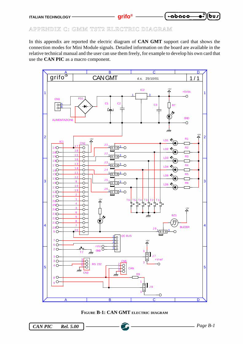
ITALIAN TECHNOLOGY grifo ®
Page B-1 CAN PIC Rel. 5.00
APPENDIX C: GMM TST2 ELECTRIC DIAGRAM
In this appendix are reported the electric diagram of CAN GMT support card that shows theconnection modes for Mini Module signals. Detailed information on the board are available in therelative technical manual and the user can use them freely, for example to develop his own card thatuse the CAN PIC as a macro component.
FIGURE B-1: CAN GMT ELECTRIC DIAGRAM
A
A
B
B
C
C
D
D
1 1
2 2
3 3
4 4
5 5
gri fo CAN GMT d.s. 25/10/01 1 / 1R
C2
1 3
IC2
C3 R7
+5V
R1
R2
R3
R4
R5
R6
+5V
T6 T5 T4 T3 T2 T1
51432 I2C BUS
AB
CN1
+5V
+5V
GND
+5Vdc
1 6
1 0
1 1
1 2
2 62 5
2 4
2 3
2 2
2 05
7
6
2
1
3
4
8
9
2 81 9
1 7
1 5
1 4
325
+5V
T7
273
R9
1 8
1 3
2 1
2 7
+5V
••
BZ1
+Vref
1 8
1 5
1 6
1 3
1 4
1 1
1 2
9
1 0
2
1
4
3
6
5
8
7
2 0
1 7
+Vcc
GND
1 9
+-
PD1
+
C1
LD1
LD2
LD3
LD4
LD5
LD6
1 3J 2
1 3J 3
1 3J 4
1 3J 5
1 3J 6
1 3J 1
1 3J 9
J 7
J 8
3
3
ALIMENTAZIONE
RS 232CN5
1
1
IC1 CN2
CAN
CN3
BUZZER

grifo ® ITALIAN TECHNOLOGY
Page B-2 CAN PIC Rel. 5.00

ITALIAN TECHNOLOGY grifo ®
Page C-1 CAN PIC Rel. 5.00
APPENDIX C: ALPHABETICAL INDEX
A
A/D CONVERTER 10, 12, 15, 20ANALOG COMPARATORS 10, 12, 15, 20
B
BACK UP 10, 13, 17, 43BATTERY 10, 13, 17, 43BIBLIOGRAPHY 44
C
CAN INTERFACE 20CAN GMT 8 , 24, 26, B-1CAN INTERFACE 9, 12, 15CARD VERSION 3CCP 20CLOCK 6, 15CLOCK FREQUENCY 12CN1 14CONSUMPTION 13CPU 12CPU INTERNAL PERIPHERALS 43CRYSTAL 6CURRENT CONSUMPTION 13CURRENT LOOP 6, 9
D
DIGITAL I/O 6, 12, 15DIP SWITCH 9, 12, 16, 17, 42DSW1 18, 42
E
EEPROM 8, 12
F
FLASH 8, 12
G
GMB HR84 22, 26GMM PIC-PR 28, 32

grifo ® ITALIAN TECHNOLOGY
Page C-2 CAN PIC Rel. 5.00
H
HLVD THRESHOLD 13
I
I2C BUS 8, 10, 12, 15, 20I2C BUS PULL-UP RESISTOR 13IMPEDANCE ANALOG SIGNALS GENERATORS 13IN CIRCUIT DEBUGGER 21INT0 21INT1 21INTERRUPT 12, 15, 21ISP 15
L
LD1 42LD2 42LEDS 12, 14, 42
M
MEMORY 8MSI 01 6
P
POWER ON TIME 12POWER SUPPLY 20POWER SUPPLY VOLTAGE 13PWM 10, 12, 15
Q
QTP 8
R
REAL TIME CLOCK 10, 12RELATIVE HUMIDITY 13RESET 15RS 232 9, 12, 15, 17, 18RS 232 PROTECTION 13RS 422 6, 9RS 485 6, 9RTC 6, 8, 9, 10, 15, 43

ITALIAN TECHNOLOGY grifo ®
Page C-3 CAN PIC Rel. 5.00
S
SCL 43SDA 43SERIAL LINE 6SIZE 13SOFTWARE DESCRIPTION 40SPI 8, 12, 15, 20SRAM 8, 9, 12
T
TEMPERATURE RANGE 13TIMER/COUNTER 10, 12TTL 9, 12, 15, 17, 18, 20
V
VPP 15
W
WATCH DOG 10, 12WEIGHT 13

grifo ® ITALIAN TECHNOLOGY
Page C-4 CAN PIC Rel. 5.00