main battery loads vgate 11.5v min. - infineon … ic gate driver auir3240s v 1 201rev j 6 -04 11...
TRANSCRIPT

Automotive IC
Gate driver AUIR3240S
1 Rev J 2016-04-11
Automotive grade
LOW QUIESCENT CURRENT MOSFET DRIVER
Features Very low quiescent current on state Boost converter with integrated diode Standard level gate voltage Wide operating voltage 4-36V Temperature monitoring with NTC interface Lead-Free, Halogen Free, RoHS compliant
Applications Battery switch for Stop and Start system
Description The AUIR3240S is a high side mosfet driver for battery switch application where a very low quiescent current is required when the driver is on. The AUIR3240S is a combination of a boost DC/DC converter using an external inductor and a gate driver. It drives standard level Mosfet even at low battery voltage. The input is active low to reduce current consumption.
Product Summary
Operating voltage 4-36V Vgate 11.5V min. Iqcc On 50µA max.
Package
SO8
Typical Connection
SW
/IN
GATE
GND
VCC
Cout
500µH
Main Battery Loads
V DG IN NTC EN
NTC
NTC
R Ntc
Rs
RS Current measurement
Rs Ntc
Rin

AUIR3240S
2 Rev J 2016-04-11
Qualification Information†
Qualification Level
Automotive
(per AEC-Q100)
Comments: This family of ICs has passed an Automotive qualification. IR’s Industrial and Consumer qualification level is granted by extension of the higher Automotive level.
Moisture Sensitivity Level SOIC-8L MSL2,
260°C
(per IPC/JEDEC J-STD-020)
ESD
Machine Model Class M0 (+/-50V)
(per AEC-Q100-003)
Human Body Model Class H0 (+/-50V)
(per AEC-Q100-002)
Charged Device Model Class C4 (+/-1000V) (per AEC-Q100-011)
IC Latch-Up Test Yes
RoHS Compliant Yes
† Qualification standards can be found at International Rectifier’s web site http://www.irf.com/
AUIR3240S
3 Rev J 2016-04-11
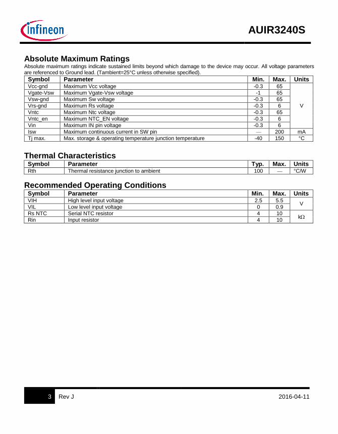
Absolute Maximum Ratings Absolute maximum ratings indicate sustained limits beyond which damage to the device may occur. All voltage parameters are referenced to Ground lead. (Tambient=25°C unless otherwise specified).
Symbol Parameter Min. Max. Units Vcc-gnd Maximum Vcc voltage -0.3 65
V
Vgate-Vsw Maximum Vgate-Vsw voltage -1 65
Vsw-gnd Maximum Sw voltage -0.3 65
Vrs-gnd Maximum Rs voltage -0.3 6
Vntc Maximum Ntc voltage -0.3 65
Vntc_en Maximum NTC_EN voltage -0.3 6
Vin Maximum IN pin voltage -0.3 6
Isw Maximum continuous current in SW pin 200 mA
Tj max. Max. storage & operating temperature junction temperature -40 150 °C
Thermal Characteristics
Symbol Parameter Typ. Max. Units Rth Thermal resistance junction to ambient 100 °C/W
Recommended Operating Conditions Symbol Parameter Min. Max. Units VIH High level input voltage 2.5 5.5
V VIL Low level input voltage 0 0.9
Rs NTC Serial NTC resistor 4 10 k
Rin Input resistor 4 10
AUIR3240S
4 Rev J 2016-04-11
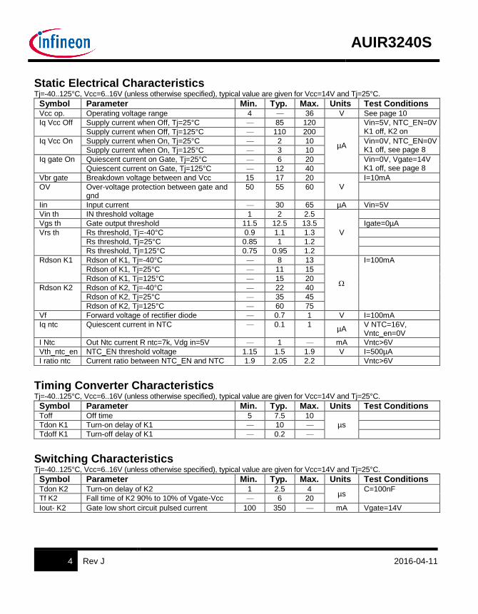
Static Electrical Characteristics Tj=-40..125°C, Vcc=6..16V (unless otherwise specified), typical value are given for Vcc=14V and Tj=25°C.
Symbol Parameter Min. Typ. Max. Units Test Conditions Vcc op. Operating voltage range 4 36 V See page 10
Iq Vcc Off Supply current when Off, Tj=25°C 85 120
µA
Vin=5V, NTC_EN=0V K1 off, K2 on Supply current when Off, Tj=125°C 110 200
Iq Vcc On Supply current when On, Tj=25°C 2 10 Vin=0V, NTC_EN=0V K1 off, see page 8 Supply current when On, Tj=125°C 3 10
Iq gate On Quiescent current on Gate, Tj=25°C 6 20 Vin=0V, Vgate=14V K1 off, see page 8 Quiescent current on Gate, Tj=125°C 12 40
Vbr gate Breakdown voltage between and Vcc 15 17 20
V
I=10mA
OV Over-voltage protection between gate and gnd
50 55 60
Iin Input current 30 65 µA Vin=5V
Vin th IN threshold voltage 1 2 2.5
V
Vgs th Gate output threshold 11.5 12.5 13.5 Igate=0µA
Vrs th Rs threshold, Tj=-40°C 0.9 1.1 1.3
Rs threshold, Tj=25°C 0.85 1 1.2
Rs threshold, Tj=125°C 0.75 0.95 1.2
Rdson K1 Rdson of K1, Tj=-40°C 8 13
I=100mA
Rdson of K1, Tj=25°C 11 15
Rdson of K1, Tj=125°C 15 20
Rdson K2 Rdson of K2, Tj=-40°C 22 40
Rdson of K2, Tj=25°C 35 45
Rdson of K2, Tj=125°C 60 75
Vf Forward voltage of rectifier diode 0.7 1 V I=100mA
Iq ntc Quiescent current in NTC 0.1 1 µA
V NTC=16V, Vntc_en=0V
I Ntc Out Ntc current R ntc=7k, Vdg in=5V 1 mA Vntc>6V
Vth_ntc_en NTC_EN threshold voltage 1.15 1.5 1.9 V I=500µA
I ratio ntc Current ratio between NTC_EN and NTC 1.9 2.05 2.2 Vntc>6V
Timing Converter Characteristics Tj=-40..125°C, Vcc=6..16V (unless otherwise specified), typical value are given for Vcc=14V and Tj=25°C.
Symbol Parameter Min. Typ. Max. Units Test Conditions Toff Off time 5 7.5 10
µs
Tdon K1 Turn-on delay of K1 10
Tdoff K1 Turn-off delay of K1 0.2
Switching Characteristics Tj=-40..125°C, Vcc=6..16V (unless otherwise specified), typical value are given for Vcc=14V and Tj=25°C.
Symbol Parameter Min. Typ. Max. Units Test Conditions Tdon K2 Turn-on delay of K2 1 2.5 4
µs C=100nF
Tf K2 Fall time of K2 90% to 10% of Vgate-Vcc 6 20
Iout- K2 Gate low short circuit pulsed current 100 350 mA Vgate=14V

AUIR3240S
5 Rev J 2016-04-11
Lead Definitions Pin number Symbol Description
1 NTC An NTC resistor can be connected between this pin and the Vcc line close to the tab to sense the temperature of the Mosfet
2 NTC_EN NTC_EN is the input of the NTC system.
3 /IN Active low input pin to enable the boost converter or short the gate to Vcc
4 GND Ground pin
5 RS Current sense input pin
6 SW Output of K1
7 VCC Power supply
8 GATE Output of the boost converter
Lead Assignments
1 2 3 4
SO8
8 7 6 5 1- NTC 2- NTC_EN 3- /IN 4- GND 5- RS 6- SW 7- VCC 8- GATE
AUIR3240S
6 Rev J 2016-04-11
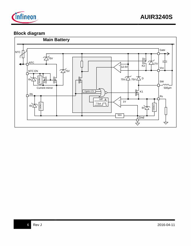
Block diagram
Vgate>OV
SW
/IN
Gate
Gnd
Vcc
K1
K2
500µH
Main Battery
NTC EN
NTC
NTC
Rs
Current mirror
17V
D
-
+
75V -
+
75V
1V
12.5V
15
0k
6V
15
0k
50
75V
50
0k
6V
7.5µs
toff
6V
75V

AUIR3240S
7 Rev J 2016-04-11
Description
The topology of the AUIR3240S is a boost DC/DC converter working in current mode. K1 is switched on when the gate voltage is lower than Vgs threshold. When Rs pin reaches Vrs th, K1 is turned off and the inductor charge the gate capacitor through D. The system cannot restart during Toff after Vrs th has been reached. The DC/DC restart only when the Gate and the Vcc voltage difference is lower than 12.5V in order to achieve low quiescent current on the power supply. To turn off the power Mosfet, the input must be pull high. Then the DC/DC converter is turned and K2 shorts the gate to Vcc.
Vin
Irs
Vgs
Ipeak
Vgs threshold
Parameters definition Current definition
/IN
GATE
GND
VCC NTC EN
NTC
RS
SW
Iq NTC Iq gate On
Iq Vcc Off Iq Vcc On
I out leakage

AUIR3240S
8 Rev J 2016-04-11
Timing definition
Vin
Ik1
Vgate-Vcc
Toff
Ipeak
Vgsth
IL
Ipeak=Vrs th/Rs
tdischarge
ton
T
Vgate peak
Vrs
Vgate-Vcc
Vrsth
Vgs threshold
Tdon K1 Tdoff K1
Low quiescent current operation when On. The AUIR3240S is able to operate with a very low quiescent current on the Vcc pin. Nevertheless the supply current depends also on the leakage of the power mosfet named “I out leakage” on the diagram below. The leakage current is given when K1 is off. When K1 is on, the current flowing in Vcc is the current charging the inductor. Therefore the average current on the Vcc is the combination of the current when K1 is ON and OFF. The average current on the Vcc pin can be calculated using:

AUIR3240S
9 Rev J 2016-04-11
Ivcc ave = (Iq gate + Iout leakage) ∗Vgate − Vcc + Vf
Vcc+ Iq Vcc on + Iq gate on + Iq NTC
With Vgate: the average voltage on the output. Vgate average = (Vgate peak + Vgsth)/2 Vgate peak can be calculated by:
Vgate peak = √L
Cout. Ipeak2 + Vgsth2
During On operation, the DC/DC works in pulse mode, meaning each time the Vgate-Vcc voltage comes below 12.5V, the AUIR3240S switches on K1 to recharge the gate voltage. When the Iout leakage is low enough to maintain the DC/DC in discontinuous mode, the frequency is calculate by:
T =Ipeak2∗L
2∗(Iq gate+Iout leakage)∗(Vgate−Vcc+Vf)
Peak current control The current in the inductor is limited by the 1V comparator which monitors the voltage across Rs. Due to the delay in the
loop (tdoff K1), the inductor current will exceed the threshold set by: Vrsth
Rs
At low voltage, the current waveform in the inductor is not anymore linear, but exponential because the sum of the resistor of K1, the inductor and RS are not any more negligible.
Vrs
Vrsth
tdoff K1 t Vrsth
t on
The peak current and ton can be calculated as follow:
t Vrsth = −L
Rk1 + Rs + Rl∗ ln (1 −
(Rs + Rk1 + Rl) ∗ Vrsth
Rs ∗ Vcc)
Where Rl is the resistor of the inductor
With : t on = t Vrsth + tdoff K1 The peak current can be solved by:
Ipeak =Vcc
Rk1 + Rs + Rl∗ (1 − e−ton∗
Rk1+Rs+RlL )
AUIR3240S
10 Rev J 2016-04-11
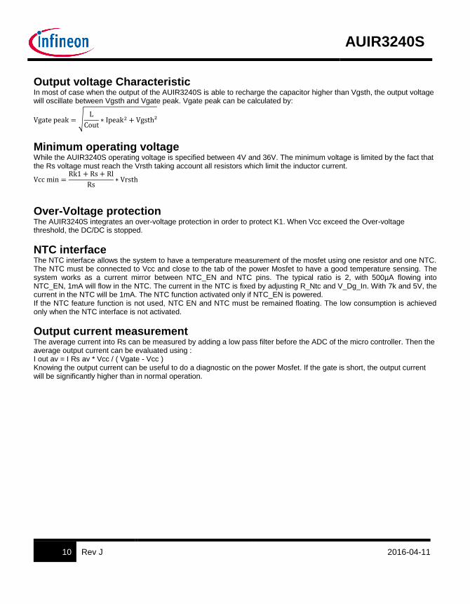
Output voltage Characteristic In most of case when the output of the AUIR3240S is able to recharge the capacitor higher than Vgsth, the output voltage will oscillate between Vgsth and Vgate peak. Vgate peak can be calculated by:
Vgate peak = √L
Cout∗ Ipeak2 + Vgsth²
Minimum operating voltage While the AUIR3240S operating voltage is specified between 4V and 36V. The minimum voltage is limited by the fact that the Rs voltage must reach the Vrsth taking account all resistors which limit the inductor current.
Vcc min =Rk1 + Rs + Rl
Rs∗ Vrsth
Over-Voltage protection The AUIR3240S integrates an over-voltage protection in order to protect K1. When Vcc exceed the Over-voltage threshold, the DC/DC is stopped.
NTC interface The NTC interface allows the system to have a temperature measurement of the mosfet using one resistor and one NTC. The NTC must be connected to Vcc and close to the tab of the power Mosfet to have a good temperature sensing. The system works as a current mirror between NTC_EN and NTC pins. The typical ratio is 2, with 500µA flowing into NTC_EN, 1mA will flow in the NTC. The current in the NTC is fixed by adjusting R_Ntc and V_Dg_In. With 7k and 5V, the current in the NTC will be 1mA. The NTC function activated only if NTC_EN is powered. If the NTC feature function is not used, NTC EN and NTC must be remained floating. The low consumption is achieved only when the NTC interface is not activated.
Output current measurement The average current into Rs can be measured by adding a low pass filter before the ADC of the micro controller. Then the average output current can be evaluated using : I out av = I Rs av * Vcc / ( Vgate - Vcc ) Knowing the output current can be useful to do a diagnostic on the power Mosfet. If the gate is short, the output current will be significantly higher than in normal operation.
AUIR3240S
11 Rev J 2016-04-11
Iq G
ate
on, G
ate
le
akage c
urr
ent
(µA
)
Tj, junction temperature (°C)
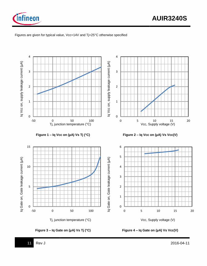
Figure 1 – Iq Vcc on (µA) Vs Tj (°C)
0
1
2
3
4
-50 0 50 100
Iq V
cc o
n, supply
le
akage c
urr
ent (µ
A)
Vcc, Supply voltage (V)
Figure 2 – Iq Vcc on (µA) Vs Vcc(V)
0
1
2
3
4
0 5 10 15 20
Iq V
cc o
n, supply
le
akage c
urr
ent (µ
A)
0
5
10
15
-50 0 50 100
Figure 3 – Iq Gate on (µA) Vs Tj (°C)
Tj, junction temperature (°C)
Figure 4 – Iq Gate on (µA) Vs Vcc(V)
Vcc, Supply voltage (V)
Iq G
ate
on, G
ate
le
akage c
urr
ent
(µA
)
0
1
2
3
4
5
6
0 5 10 15 20
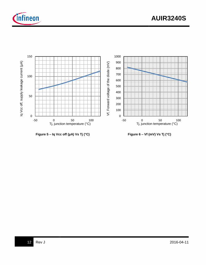
Figures are given for typical value, Vcc=14V and Tj=25°C otherwise specified
AUIR3240S
12 Rev J 2016-04-11
Iq V
cc o
ff, supply
le
akage c
urr
ent (µ
A)
0
50
100
150
-50 0 50 100
Figure 5 – Iq Vcc off (µA) Vs Tj (°C)
Tj, junction temperature (°C)
Vf, F
orw
ard
voltage o
f th
e d
iode (
mV
)
0
100
200
300
400
500
600
700
800
900
1000
-50 0 50 100
Figure 6 – Vf (mV) Vs Tj (°C)
Tj, junction temperature (°C)
AUIR3240S
13 Rev J 2016-04-11
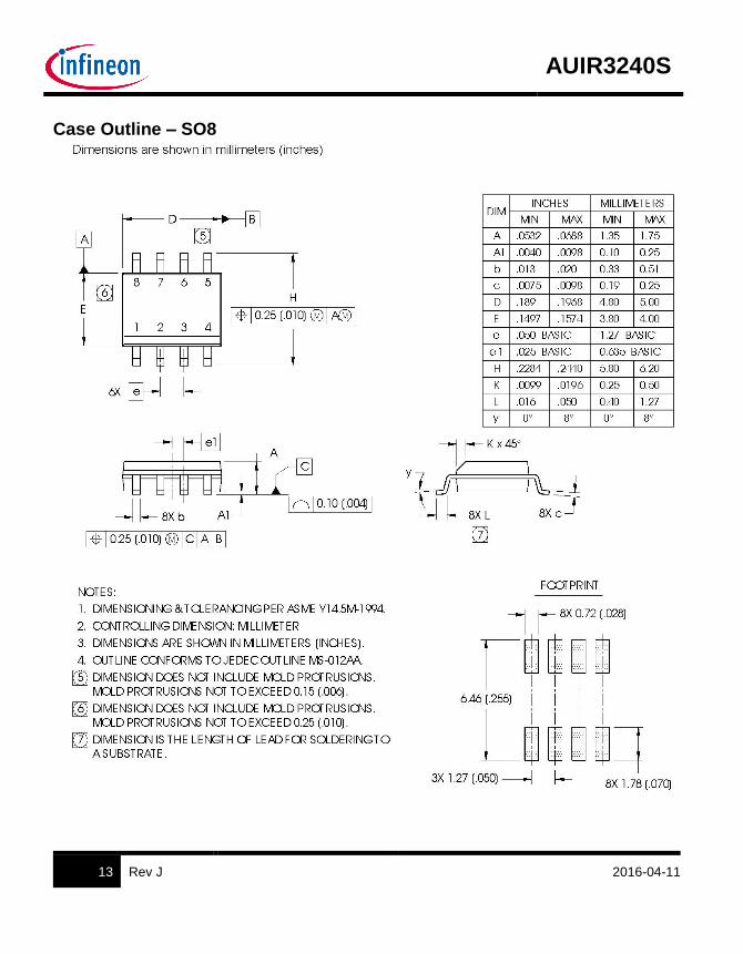
Case Outline – SO8

AUIR3240S
14 Rev J 2016-04-11
Tape & Reel SO8

AUIR3240S
15 Rev J 2016-04-11
Part Marking Information
Ordering Information
Base Part Number Package Type Standard Pack
Complete Part Number Form Quantity
AUIR3240S SOIC8 Tape and reel 2500 AUIR3240STR
AUIR3240S
16 Rev J 2016-04-11
Published by Infineon Technologies AG 81726 München, Germany
© Infineon Technologies AG 2015
All Rights Reserved. IMPORTANT NOTICE The information given in this document shall in no event be regarded as a guarantee of conditions or characteristics (“Beschaffenheitsgarantie”). With respect to any examples, hints or any typical values stated herein and/or any information regarding the application of the product, Infineon Technologies hereby disclaims any and all warranties and liabilities of any kind, including without limitation warranties of non-infringement of intellectual property rights of any third party. In addition, any information given in this document is subject to customer’s compliance with its obligations stated in this document and any applicable legal requirements, norms and standards concerning customer’s products and any use of the product of Infineon Technologies in customer’s applications. The data contained in this document is exclusively intended for technically trained staff. It is the responsibility of customer’s technical departments to evaluate the suitability of the product for the intended application and the completeness of the product information given in this document with respect to such application. For further information on the product, technology, delivery terms and conditions and prices please contact your nearest Infineon Technologies office (www.infineon.com). WARNINGS
Due to technical requirements products may contain dangerous substances. For information on the types in question please contact your nearest Infineon Technologies office. Except as otherwise explicitly approved by Infineon Technologies in a written document signed by authorized representatives of Infineon Technologies, Infineon Technologies’ products may not be used in any applications where a failure of the product or any consequences of the use thereof can reasonably be expected to result in personal injury.

AUIR3240S
17 Rev J 2016-04-11
Revision History Revision Date Notes/Changes
A December 10th, 2011 Initial release
B March, 28th 2012 Page4 correct temperature condition for Vrsth +125°C
C April, 2nd 2012 Update maximum operating temperature
D July, 17th 2012 Update page 4, Tdon K1 typ.
E November, 19th 2012 Update formula page 9 tVrsth
F October, 17th 2013 Update NTC interface current page10
G October 31, 2014 Update limit max Rdson K2
H October 10, 2015 Update the template Update OV definition Update ordering information
I December 21, 216 Update Ivcc formula page 9
J April 11, 2016 Update Tdon K1 and Tdoff K1