mahdi abbasi abbasi@basu ac [email protected] filelecture 13: sequential logic counters and...
TRANSCRIPT

Sequential Logic Counters and RegistersCounters and Registers
Mahdi Abbasi
abbasi@basu ac [email protected]

Outline
Counters
Introduction: Counters
h ( i l ) Asynchronous (Ripple) Counters
Asynchronous Counters with MOD number < 2n
Asynchronous Down Countersy
Cascading Asynchronous Counters
2
Lecture 13: Sequential Logic Counters and RegistersCounters and Registers
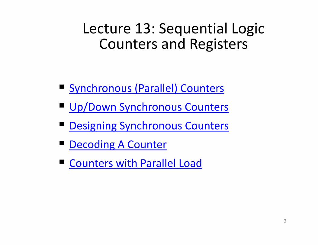
Synchronous (Parallel) Counters
Up/Down Synchronous Counters Up/Down Synchronous Counters
Designing Synchronous Counters
Decoding A Counter
Counters with Parallel Load
3

Lecture 13: Sequential Logic Counters and RegistersCounters and Registers
Registers
Introduction: RegistersSimple RegistersR i t ith P ll l L dRegisters with Parallel Load
Using Registers to implement Sequential Circuits
Shift RegistersSerial In/Serial Out Shift RegistersSerial In/Parallel Out Shift RegistersSerial In/Parallel Out Shift RegistersParallel In/Serial Out Shift RegistersParallel In/Parallel Out Shift Registers
4

Lecture 13: Sequential Logic Counters and RegistersCounters and Registers
Bidirectional Shift Registers
An Application – Serial AdditionAn Application Serial Addition
Shift Register CountersRing CountersRing CountersJohnson Counters
Random-Access Memory (RAM)Random Access Memory (RAM)
5

Introduction: CountersIntroduction: Counters Counters are circuits that cycle through a specified
number of states.number of states.
Two types of counters: synchronous (parallel) counters synchronous (parallel) countersasynchronous (ripple) counters
Ripple counters allow some flip-flop outputs to be pp p p pused as a source of clock for other flip-flops.
Synchronous counters apply the same clock to all flip-flops.
6

Asynchronous (Ripple) CountersAsynchronous (Ripple) Counters
Asynchronous counters: the flip-flops do not h l h h dchange states at exactly the same time as they do
not have a common clock pulse. Also known as ripple counters as the input clockAlso known as ripple counters, as the input clock
pulse “ripples” through the counter – cumulative delay is a drawback.
fl fl ( d l ) n n flip-flops a MOD (modulus) 2n counter. (Note: A MOD-x counter cycles through x states.) Output of the last flip-flop (MSB) divides theOutput of the last flip-flop (MSB) divides the
input clock frequency by the MOD number of the counter, hence a counter is also a frequency dividerdivider.
7

Asynchronous (Ripple) CountersAsynchronous (Ripple) Counters Example: 2-bit ripple binary counter.
O t t f fli fl i t d t th l k Output of one flip-flop is connected to the clock input of the next more-significant flip-flop.
HIGH
K
J
K
JQ0 Q1
Q0CLK CC
FF1FF0
4321CLK
Q Timing diagram
00 01 10 11 00 ...
Q0
Q0 1 10 0 0
8
Q1 1 10 0 0

Asynchronous (Ripple) CountersAsynchronous (Ripple) Counters Example: 3-bit ripple binary counter.
HIGH
K
J
K
JQ0 Q1
Q0CC
K
J
Q1C
Q2
CLK
HIGH
K K
FF1FF0KFF2
4321CLK 87654321CLK
Q0
Q1
1 1
1 1
0
0 0
0 0
0
8765
1 10 0
1 10 01
Q2 0 00 0 1 1 11 0
Recycles back to 0
9

Asynchronous (Ripple) CountersAsynchronous (Ripple) Counters Propagation delays in an asynchronous (ripple-
clocked) binary counter.) y
If the accumulated delay is greater than the clock pulse, some counter states may be misrepresented!
4321CLK
Q0Q0
Q1
Q2
tPLH(CLK to Q0)
tPHL (CLK to Q0)tPLH (Q0 to Q1)
tPHL (CLK to Q0)tPHL (Q0 to Q1)tPLH (Q1 to Q2)
10
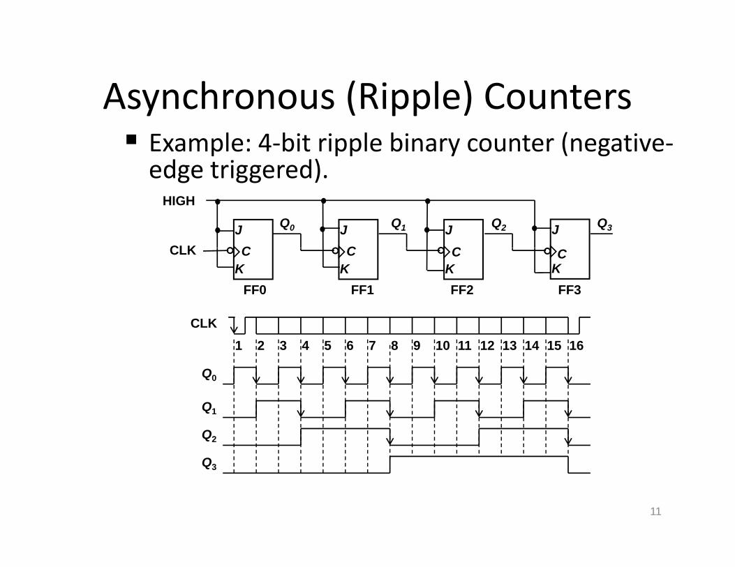
Asynchronous (Ripple) CountersAsynchronous (Ripple) Counters Example: 4-bit ripple binary counter (negative-
edge triggered).edge triggered).
J J Q1Q0
CCJC
Q2
CLK
HIGH
J Q3
K KFF1FF0
CCKC
FF2
CLKKC
FF3
CLKCLK1 2 3 4 5 6 7 8 9 10 11 12 13 14 15 16
Q0
Q1
Q2
Q
11
Q3

Asyn. Counters with MOD no. < 2nAsyn. Counters with MOD no. < 2 States may be skipped resulting in a truncated
sequence.q
Technique: force counter to recycle before going through all of the states in the binary sequence.
Example: Given the following circuit, determine the counting sequence (and hence the modulus no.)
JQCLK
JQCLK
JQCLK
C B A
All J, KKQ
CLRKQ
CLRKQ
CLR
BC
inputs are 1 (HIGH).
12
C

Asyn. Counters with MOD no. < 2nAsyn. Counters with MOD no. < 2 Example (cont’d):
JQJQJQC B A
K
JQ
QCLK
CLRK
JQ
QCLK
CLRK
JQ
QCLK
CLR
All J, Kinputs are 1
BC
are 1 (HIGH).
A
B
1 2 3 4 5 6 7 8 9 10 11 12Clock MOD-6 counter
produced by clearing (a MOD-8
B
C
NAND 1
g (binary counter) when count of six (110) occurs.
13
Output 0

Asyn. Counters with MOD no. < 2nAsyn. Counters with MOD no. < 2 Example (cont’d): Counting sequence of
circuit (in CBA order).( )
A
B
1 2 3 4 5 6 7 8 9 10 11 12Clock
0
0
1
0
0
1
1
1
0
0
1
0
0
0
1
0BC
NANDOutput
10
0
0
0
0
1
0
1
0
0
1
0
1
0
0
0
0
111 000001Temporary
state Counter is a MOD-6 110
101
010
011
counter.
14
100

Asyn. Counters with MOD no. < 2nAsyn. Counters with MOD no. < 2 Exercise: How to construct an asynchronous MOD-
5 counter? MOD-7 counter? MOD-12 counter?5 counter? MOD 7 counter? MOD 12 counter?
Question: The following is a MOD-? counter?
K
JQ
QCLR
C B A
K
JQ
QCLR
K
JQ
QCLR
K
JQ
QCLR
K
JQ
QCLR
K
JQ
QCLR
DEF
CLR
CD
CLRCLRCLRCLRCLR
DEF All J = K = 1.
15

Asyn. Counters with MOD no. < 2nAsyn. Counters with MOD no. < 2 Decade counters (or BCD counters) are counters
with 10 states (modulus-10) in their sequence. ( ) qThey are commonly used in daily life (e.g.: utility meters, odometers, etc.).
Design an asynchronous decade counter Design an asynchronous decade counter.
HIGH
(A.C)'
D
CLK
HIGH
K
J
C
Q
K
J
C
QC
K
J
C
QB
K
J
C
QA
KCLR
KCLR
KCLR
KCLR
16

Asyn. Counters with MOD no. < 2nAsyn. Counters with MOD no. < 2 Asynchronous decade/BCD counter (cont’d).
D
CLK
HIGH
K
JC
CLR
Q
K
JC
CLR
QC
K
JC
CLR
QB
K
JC
CLR
QA (A.C)'
1 2 3 4 5 6 7 8 9 10Clock
11
CLR CLR CLR CLR
D
C
B
0
0
1
0
0
1
1
1
0
0
1
0
0
1
1
1
0
0
1
0
0
0
B
NAND output
A0
0
0
0
0
0
0
0
1
0
1
0
1
0
1
0
0
1
0
1
0
0
17
output
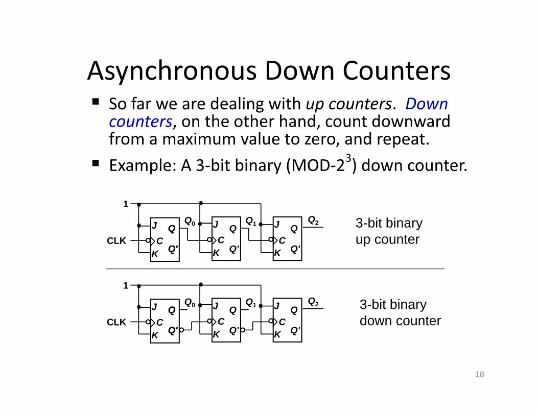
Asynchronous Down CountersAsynchronous Down Counters So far we are dealing with up counters. Down
counters, on the other hand, count downward , ,from a maximum value to zero, and repeat.
Example: A 3-bit binary (MOD-23) down counter.
J J Q1Q0 J Q2
1
Q Q QQ 3-bit binary
K KCC
KCCLK
Q' Q' Q'Q'up counter
1
3-bit binary down counter
1
K
J
K
J Q1Q0
CCK
JC
Q2
CLKQ
Q'
Q
Q'
Q
Q'
Q
Q'
18

Asynchronous Down CountersAsynchronous Down Counters Example: A 3-bit binary (MOD-8) down counter.
000001
000111
010 110
1
J J Q1Q0 J Q2Q Q QQ
011100
101K KCC
KCCLK
Q
Q'
Q
Q'
Q
Q'
Q
Q'
4321CLK
Q0 1 10 0 0
8765
1 10 0
Q1 1 00 1 0 1 01 0
Q2 1 10 1 1 0 00 0
19

Cascading Asynchronous CountersCascading Asynchronous Counters Larger asynchronous (ripple) counter can be
constructed by cascading smaller ripple counters. Connect last-stage output of one counter to the
clock input of next counter so as to achieve higher-modulus operation. Example: A modulus-32 ripple counter constructed
from a modulus-4 counter and a modulus-8 counter.
J J
Q1Q0
Q QQ J J
Q3Q2
J
Q4
Q Q QQ
K
J
K
JCCCLK
Q
Q'
Q
Q'
Q
Q' K
J
K
JCC
K
JC
Q
Q'
Q
Q'
Q
Q'
Q
Q'
Modulus 4 counter Modulus 8 counter
20
Modulus-4 counter Modulus-8 counter

Cascading Asynchronous CountersCascading Asynchronous Counters Example: A 6-bit binary counter (counts from
0 to 63) constructed from two 3-bit counters.0 to 63) constructed from two 3 bit counters. A0 A1 A2 A3 A4 A5
3-bit binary counter
3-bit binary counter
Count pulse
A5 A4 A3 A2 A1 A0
0 0 0 0 0 00 0 0 0 0 10 0 0 : : :0 0 0 : : :0 0 0 1 1 10 0 1 0 0 00 0 1 0 0 1
Cascading Asynchronous Counters 21
: : : : : :
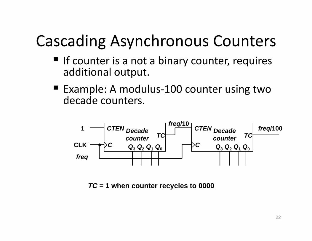
Cascading Asynchronous CountersCascading Asynchronous Counters If counter is a not a binary counter, requires
additional output.additional output.
Example: A modulus-100 counter using two decade counters.
Decade CTENTC
1 Decade CTENTC
freq/10freq/100
CLKcounterQ3 Q2 Q1 Q0
CTC counter
Q3 Q2 Q1 Q0C
TC
freq
TC = 1 when counter recycles to 0000
22

Synchronous (Parallel) CountersSynchronous (Parallel) Counters Synchronous (parallel) counters: the flip-flops are
clocked at the same time by a common clock pulse.
We can design these counters using the sequential logic design process (covered in Lecture #12).
E l 2 bit h bi t ( i T Example: 2-bit synchronous binary counter (using T flip-flops, or JK flip-flops with identical J,K inputs).
Present Next Flip-flopstate state inputs
A1 A0 A1+ A0
+ TA1 TA00100
0 0 0 1 0 10 1 1 0 1 11 0 1 1 0 11 1 0 0 1 1
1011
23

Synchronous (Parallel) CountersSynchronous (Parallel) Counters Example: 2-bit synchronous binary counter (using T
flip-flops, or JK flip-flops with identical J,K inputs).
Present Next Flip-flopstate state inputs
A1 A0 A1+ A0
+ TA1 TA0 TA1 = A00 0 0 1 0 10 1 1 0 1 11 0 1 1 0 11 1 0 0 1 1
1 0
TA0 = 1
1
J J A1A0Q QQ
K KCC
CLK
Q' Q'Q'
24

Synchronous (Parallel) CountersSynchronous (Parallel) Counters Example: 3-bit synchronous binary counter (using T
flip-flops, or JK flip-flops with identical J, K inputs).Present Next Flip-flop
state state inputsA2 A1 A0 A2
+ A1+ A0
+ TA2 TA1 TA0
0 0 0 0 0 1 0 0 10 0 0 0 0 1 0 0 10 0 1 0 1 0 0 1 10 1 0 0 1 1 0 0 10 1 1 1 0 0 1 1 11 0 0 1 0 1 0 0 11 0 0 1 0 1 0 0 11 0 1 1 1 0 0 1 11 1 0 1 1 1 0 0 11 1 1 0 0 0 1 1 1
A1 A1 A1
A2
A0
11
A2
A0
11 1
1A2
A0
1 1 111 1 1
1
25
TA2 = A1.A0
A0
TA1 = A0 TA0 = 1A0 A0

Synchronous (Parallel) CountersSynchronous (Parallel) Counters Example: 3-bit synchronous binary counter (cont’d).
TA2 = A1.A0 TA1 = A0TA0 = 1
A2 A1 A0
KQ
J KQ
J KQ
J
1CP
26

Synchronous (Parallel) CountersSynchronous (Parallel) Counters Note that in a binary counter, the nth bit (shown
underlined) is always complemented wheneverunderlined) is always complemented whenever011…11 100…00
or 111…11 000…00or 111…11 000…00
Hence, Xn is complemented whenever Xn-1Xn-2 ... X1X0 = 11…11.n 1 n 2 1 0
As a result, if T flip-flops are used, then TXn = Xn-1 . Xn-2 . ... . X1 . X0
27

Synchronous (Parallel) CountersSynchronous (Parallel) Counters Example: 4-bit synchronous binary counter.
TA3 = A2 . A1 . A0TA3 A2 . A1 . A0TA2 = A1 . A0TA1 = A0TA = 1TA0 = 1
1 A1.A0 A2.A1.A0
K
J
K
J A1A0
CCQ
Q'
Q
Q'
Q
Q' K
J A2
CQ
Q' K
J A3
CQ
Q'
CLK
28

Synchronous (Parallel) CountersSynchronous (Parallel) Counters Example: Synchronous decade/BCD counter.
Clock pulse Q3 Q2 Q1 Q0
Initially 0 0 0 01 0 0 0 12 0 0 1 0
T0 = 1
T Q ' Q2 0 0 1 03 0 0 1 14 0 1 0 05 0 1 0 16 0 1 1 0
T1 = Q3'.Q0
T2 = Q1.Q0
T = Q Q Q + Q Q7 0 1 1 18 1 0 0 09 1 0 0 1
10 (recycle) 0 0 0 0
T3 = Q2.Q1.Q0 + Q3.Q0
29

Synchronous (Parallel) CountersSynchronous (Parallel) Counters Example: Synchronous decade/BCD counter
(cont’d).( )
T0 = 1T1 = Q3'.Q0
T2 = Q1.Q0
T3 = Q2.Q1.Q0 + Q3.Q0
1 Q1
Q0
T QQQ2 Q3T QQ T QQ T QQ
CLK
CQ'Q'
CQ'Q'
CQ'Q'
CQ'Q'
30

Up/Down Synchronous CountersUp/Down Synchronous Counters Up/down synchronous counter: a
bidirectional counter that is capable ofbidirectional counter that is capable of counting either up or down.
An input (control) line Up/Down (or simply p ( ) p/ ( p yUp) specifies the direction of counting.Up/Down = 1 Count upward
Up/Down = 0 Count downward
31

Up/Down Synchronous CountersUp/Down Synchronous Counters Example: A 3-bit up/down synchronous
binary counter.binary counter.Clock pulse Up Q2 Q1 Q0 Down
0 0 0 01 0 0 12 0 1 03 0 1 14 1 0 05 1 0 16 1 1 06 1 1 07 1 1 1
TQ = 1 Up counter Down counterTQ0 = 1TQ1 = (Q0.Up) + (Q0'.Up' )TQ2 = ( Q0.Q1.Up ) + (Q0'. Q1'. Up' )
Up counterTQ0 = 1TQ1 = Q0
TQ = Q Q
Down counterTQ0 = 1TQ1 = Q0’TQ = Q ’ Q ’
32
TQ2 = Q0.Q1 TQ2 = Q0 .Q1

Up/Down Synchronous CountersUp/Down Synchronous Counters Example: A 3-bit up/down synchronous
binary counter (cont’d).binary counter (cont d).TQ0 = 1TQ1 = (Q0.Up) + (Q0'.Up' )TQ2 = ( Q0.Q1.Up ) + (Q0'. Q1'. Up' )Q2 ( Q0 Q1 p ) (Q0 Q1 p )
Q1Q0
1
Q1Q0
TC
Q
Q'
Q
Q'
TC
Q
Q'
Q
Q'
TC
Q
Q'
Q
Q'Up
Q2
CLK
33

Designing Synchronous CountersDesigning Synchronous Counters Covered in Lecture #12.
E l A 3 bit G100
000001
Example: A 3-bit Gray code counter (using JK flip-flops).
101
111
011
010p p ) 111110
010
Present Next Flip-flopstate state inputs
Q2 Q1 Q0 Q2+ Q1
+ Q0+ JQ2 KQ2 JQ1 KQ1 JQ0 KQ0
0 0 0 0 0 1 0 X 0 X 1 X0 0 1 0 1 1 0 X 1 X X 00 1 0 1 1 0 1 X X 0 0 X0 1 1 0 1 0 0 X X 0 X 11 0 0 0 0 0 X 1 0 X 0 X1 0 1 1 0 0 X 0 0 X X 11 1 0 1 1 1 X 0 X 0 1 X
Designing Synchronous Counters 34
1 1 1 1 0 1 X 0 X 1 X 0

Designing Synchronous CountersDesigning Synchronous Counters 3-bit Gray code counter: flip-flop inputs.
000 01 11 10Q2
Q1Q0
1 000 01 11 10Q2
Q1Q0
X X1 000 01 11 10Q2
Q1Q0
XX10
1 X X X X1
JQ2 = Q1.Q0'
1 X XX X1
JQ1 = Q2'.Q0
1 XXXX1
JQ0 = Q2.Q1 + Q2'.Q1'= (Q2 Q1)'
1
000 01 11 10Q2
Q1Q0
X X X X 000 01 11 10Q2
Q1Q0
X X
(Q2 Q1)
000 01 11 10Q2
Q1Q0
XX 11 1
KQ2 = Q1'.Q0'1 X X 1
KQ1 = Q2.Q0
1 XX 1
KQ0 = Q2.Q1' + Q2'.Q1= Q2 Q1
35
2 1

Designing Synchronous CountersDesigning Synchronous Counters 3-bit Gray code counter: logic diagram.
JQ2 = Q1.Q0' JQ1 = Q2'.Q0 JQ0 = (Q2 Q1)'KQ2 = Q1'.Q0' KQ1 = Q2.Q0 KQ0 = Q2 Q1
Q1Q0 Q2J Q J Q J Q10 2J
C
Q
Q'K
J
C
Q
Q'K
J
C
Q
Q'KQ2'
Q
Q1'
CLK
Q0'
36

Decoding A CounterDecoding A Counter Decoding a counter involves determining
which state in the sequence the counter is in.q Differentiate between active-HIGH and active-
LOW decoding. Active-HIGH decoding: output HIGH if the
counter is in the state concerned. Active LOW decoding: output LOW if the Active-LOW decoding: output LOW if the
counter is in the state concerned.
37

Decoding A CounterDecoding A Counter Example: MOD-8 ripple counter (active-HIGH
decoding).decoding).
A'
1 2 3 4 5 6 7 8 9Clock
HIGH only on
100
B'C'
HIGH only on count of ABC = 000
A'B'
HIGH only on count of ABC = 001
Ccou t o C 00
A'BC'
HIGH only on count of ABC = 010
ABC
HIGH only on count of ABC = 111
...
38
C

Decoding A CounterDecoding A Counter Example: To detect that a MOD-8 counter is in
state 0 (000) or state 1 (001).state 0 (000) or state 1 (001).
A'
1 2 3 4 5 6 7 8 9Clock
HIGH only on
100A'B'C'A'B'C A'
B'HIGH only on count of ABC = 000 or ABC = 001
E ample To detect that a MOD 8 co nter is in the
C
Example: To detect that a MOD-8 counter is in the odd states (states 1, 3, 5 or 7), simply use C.
1 2 3 4 5 6 7 8 9 100
C
1 2 3 4 5 6 7 8 9Clock
HIGH only on count of odd states
100
Decoding A Counter 39

Counters with Parallel LoadCounters with Parallel Load Counters could be augmented with parallel load
capability for the following purposes:p y g p pTo start at a different stateTo count a different sequenceAs more sophisticated register withAs more sophisticated register with
increment/decrement functionality.
40

Counters with Parallel LoadCounters with Parallel Load Different ways of getting a MOD-6 counter:
A A A A A A A A
Count = 1Load = 0
Count = 1Clear = 1
A4 A3 A2 A1
Load
A4 A3 A2 A1
ClearLoad 0CPI4 I3 I2 I1
Clear 1CP
Inputs = 0
(a) Binary states 0,1,2,3,4,5.
I4 I3 I2 I1
Inputs have no effect(b) Binary states 0,1,2,3,4,5.( ) y , , , , , ( ) y , , , , ,
Count = 1
A4 A3 A2 A1
Count = 1
A4 A3 A2 A1
Carry-out
I4 I3 I2 I1
Count = 1Clear = 1CP
0 0 1 1
Load
I4 I3 I2 I1
Count = 1Clear = 1CP
1 0 1 0
Load
CS1104-13 Counters with Parallel Load 41
0 0 1 1(d) Binary states 3,4,5,6,7,8.
1 0 1 0(c) Binary states 10,11,12,13,14,15.

Counters with Parallel LoadCounters with Parallel Load 4-bit counter with
parallel load.
Clear CP Load Count Function0 X X X Clear to 01 X 0 0 No change1 X 0 0 No change1 1 X Load inputs1 0 1 Next state
Counters with Parallel Load 42

Introduction: RegistersIntroduction: Registers An n-bit register has a group of n flip-flops and
some logic gates and is capable of storing n bits of g g p ginformation.
The flip-flops store the information while the gates control when and how new information iscontrol when and how new information is transferred into the register.
Some functions of register:g retrieve data from register store/load new data into register (serial or parallel) shift the data within register (left or right) shift the data within register (left or right)
Introduction: Registers 43

Simple RegistersSimple Registers No external gates. Example: A 4 bit register A new 4 bit data is Example: A 4-bit register. A new 4-bit data is
loaded every clock cycle.
A A AAA3 A1 A0
DQ
DQ Q
D
A2
DQ
CPD D DD
I3 I1 I0I23 1 02
Simple Registers 44

Registers With Parallel LoadRegisters With Parallel Load Instead of loading the register at every clock pulse,
we may want to control when to load.y
Loading a register: transfer new information into the register. Requires a load control input.
Parallel loading: all bits are loaded simultaneously.
Registers With Parallel Load 45

Registers With Parallel LoadRegisters With Parallel LoadA0D Q
Load
I0
Load'.A0 + Load. I0
I0
A1D Q
I
A2D Q
I1
A3D Q
I2
CLK
3
CLEAR
I3
Registers With Parallel Load 46
CLEAR
Using Registers to implement lSequential Circuits
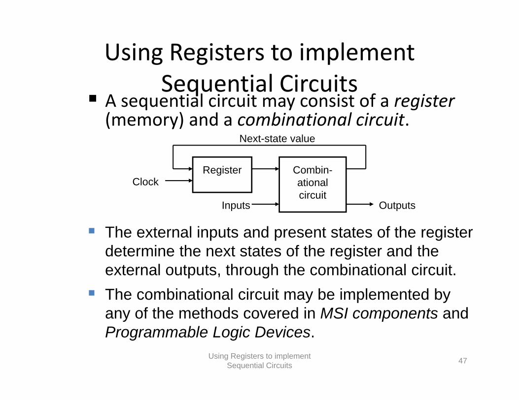
A sequential circuit may consist of a register(memory) and a combinational circuit.(memory) and a combinational circuit.
Register Combin-
Next-state value
gational circuit
Clock
Inputs Outputs
The external inputs and present states of the register determine the next states of the register and the external outputs, through the combinational circuit.p , g
The combinational circuit may be implemented by any of the methods covered in MSI components and P bl L i D i
Using Registers to implement Sequential Circuits 47
Programmable Logic Devices.

Using Registers to implement lSequential Circuits
Example 1:A1
+ = m(4,6) = A1.x'1 ( ) 1A2
+ = m(1,2,5,6) = A2.x' + A2'.x = A2 xy = m(3,7) = A2.x
Present Nextstate Input State Output
A1 A2 x A1+ A2
+ y0 0 0 0 0 00 0 0 0 0 00 0 1 0 1 00 1 0 0 1 00 1 1 0 0 11 0 0 1 0 0
A1
A2
A1.x'
A2x
1 0 0 1 0 01 0 1 0 1 01 1 0 1 1 01 1 1 0 0 1
x y
Using Registers to implement Sequential Circuits 48

Using Registers to implement lSequential Circuits
Example 2: Repeat example 1, but use a ROM.
Address Outputs1 2 3 1 2 30 0 0 0 0 00 0 0 0 0 00 0 1 0 1 00 1 0 0 1 00 1 1 0 0 11 0 0 1 0 0
A1
A28 x 3 ROM1 0 0 1 0 0
1 0 1 0 1 01 1 0 1 1 01 1 1 0 0 1
x yROM
ROM truth table
Using Registers to implement Sequential Circuits 49
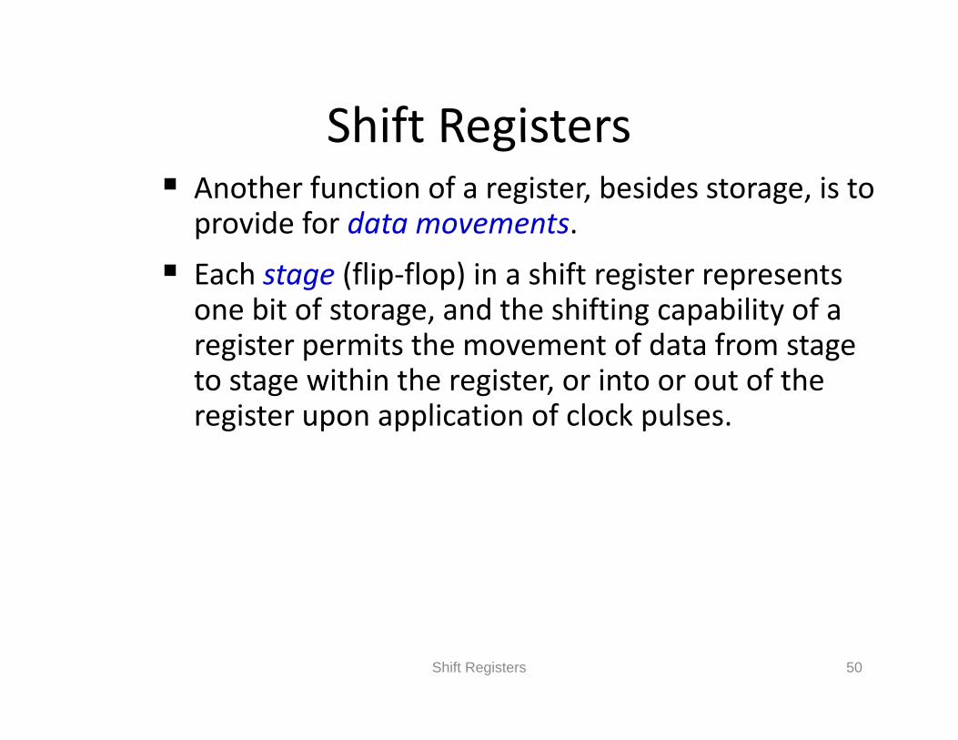
Shift RegistersShift Registers Another function of a register, besides storage, is to
provide for data movements.provide for data movements.
Each stage (flip-flop) in a shift register represents one bit of storage, and the shifting capability of a g , g p yregister permits the movement of data from stage to stage within the register, or into or out of the register upon application of clock pulsesregister upon application of clock pulses.
Shift Registers 50

Shift RegistersShift Registers Basic data movement in shift registers (four
bits are used for illustration).)
Data in Data out
(a) Serial in/shift right/serial out
Data inData out
(b) Serial in/shift left/serial out(a) Serial in/shift right/serial out (b) Serial in/shift left/serial out
Data in Data inData in
Data out
(c) Parallel in/serial outData out
(d) Serial in/parallel outData out
(e) Parallel in / parallel out
(f) Rotate right (g) Rotate left
Shift Registers 51
(f) Rotate right (g) Rotate left

Serial In/Serial Out Shift RegistersSerial In/Serial Out Shift Registers Accepts data serially – one bit at a time – and
also produces output serially.p p y
Q0 Q1 Q2 Q3Serial data Serial dataQ0D
C
QQ1 Q2 Q3Serial data
inputSerial data
outputD
C
Q D
C
Q D
C
Q
CLK
Serial In/Serial Out Shift Registers 52

Serial In/Serial Out Shift RegistersSerial In/Serial Out Shift Registers Application: Serial transfer of data from one
register to another.g
Shift register A Shift register BSI SISO SO
ClockShift control
CP
Wordtime
Clock
Shift
T1 T2 T3 T4CP
control
Serial In/Serial Out Shift Registers 53

Serial In/Serial Out Shift RegistersSerial In/Serial Out Shift Registers Serial-transfer example.
Timing Pulse Shift register A Shift register B Serial output of BInitial value 1 0 1 1 0 0 1 0 0
After T1 1 1 0 1 1 0 0 1 1After T2 1 1 1 0 1 1 0 0 0After T3 0 1 1 1 0 1 1 0 0After T4 1 0 1 1 1 0 1 1 1After T4 1 0 1 1 1 0 1 1 1
Serial In/Serial Out Shift Registers 54

Serial In/Parallel Out Shift RegistersSerial In/Parallel Out Shift Registers Accepts data serially.
O t t f ll t il bl i lt l Outputs of all stages are available simultaneously.
D
C
Q D
C
Q D
C
Q D
C
QData input
CLK
C C C C
Q0 Q1 Q2 Q3
DData input SRG 4CCLK
p
Q0 Q1 Q2 Q3
Logic symbol
Serial In/Parallel Out Shift Registers 55

Parallel In/Serial Out Shift RegistersParallel In/Serial Out Shift Registers Bits are entered simultaneously, but output is serial.
D0 D1 D2 D3
Data input
SHIFT/LOADSHIFT/LOAD
D
C
Q D
C
Q D
C
Q D
C
QQ0 Q1 Q2 Q3
Serial data out
CLK
C C C C
SHIFT.Q0 + SHIFT'.D1
Parallel In/Serial Out Shift Registers 56
0 1

Parallel In/Serial Out Shift RegistersParallel In/Serial Out Shift Registers Bits are entered simultaneously, but output is serial.
D0 D1 D2 D3
Data in
CCLKSHIFT/LOAD SRG 4
Serial data out
Logic symbol
Parallel In/Serial Out Shift Registers 57

Parallel In/Parallel Out Shift RegistersParallel In/Parallel Out Shift Registers Simultaneous input and output of all data bits.
Parallel data inputs
D0 D1 D2 D3
D
C
Q D
C
Q D
C
Q D
C
Q
Q0
CLK
Q1 Q2 Q3
Parallel data outputs
Parallel In/Parallel Out Shift Registers 58

Bidirectional Shift RegistersBidirectional Shift Registers Data can be shifted either left or right, using a
control line RIGHT/LEFT (or simply RIGHT) to ( p y )indicate the direction.
RIGHT/LEFT
Serial data in
D Q D Q D Q D QQ Q Q3RIGHT.Q0 + RIGHT' Q
CLK
C C C C
Q0
Q1 Q2 3RIGHT'.Q2
Bidirectional Shift Registers 59
CLK
Bidirectional Shift RegistersBidirectional Shift Registers 4-bit bidirectional shift register with parallel load.
Parallel outputs
Q Q Q QCl
A4 A3 A2 A1
Parallel outputs
CLK
D D D DClear
4x1 MUX
s1
s03 2 1 0
4x1 MUX
3 2 1 0
4x1 MUX
3 2 1 0
4x1 MUX
3 2 1 0
I4 I3 I2 I1
Serial input for
shift-rightSerial
input for hift l ft
Bidirectional Shift Registers 60
I4 I3 I2 I1 shift-left
Parallel inputs

Bidirectional Shift RegistersBidirectional Shift Registers 4-bit bidirectional shift register with parallel load.
Mode Controls1 s0 Register Operation0 0 No change0 1 Shift right1 0 Shift left1 1 Parallel load
Bidirectional Shift Registers 61

An Application – Serial AdditionAn Application Serial Addition Most operations in digital computers are done
in parallel. Serial operations are slower butin parallel. Serial operations are slower but require less equipment.
A serial adder is shown below. A A + B.
FAx SShift-register AShift-rightSI
SOFAy
zSC
Shift-register ACP
Shift register B
SIExternal input SO
Shift-register BQ D
An Application – Serial Addition 62
Clear

An Application – Serial AdditionAn Application Serial Addition A = 0100; B = 0111. A + B = 1011 is stored in
A after 4 clock pulses. p
Initial: A: 0 1 0 0B: 0 1 1 1
Q: 0
Step 1: 0 + 1 + 0S = 1, C = 0
A: 1 0 1 0B: x 0 1 1
Q: 0
Step 2: 0 + 1 + 0 A: 1 1 0 1 Q 0Step 2: 0 + 1 + 0S = 1, C = 0
A: 1 1 0 1B: x x 0 1
Q: 0
Step 3: 1 + 1 + 0S = 0 C = 1
A: 0 1 1 0B 0
Q: 1S = 0, C = 1 B: x x x 0
Step 4: 0 + 0 + 1S = 1, C = 0
A: 1 0 1 1B: x x x x
Q: 0
An Application – Serial Addition 63

Shift Register CountersShift Register Counters Shift register counter: a shift register with the serial
output connected back to the serial input.output connected back to the serial input.
They are classified as counters because they give a specified sequence of states.p q
Two common types: the Johnson counter and the Ring counter.
Shift Register Counters 64

Ring CountersRing Counters One flip-flop (stage) for each state in the sequence.
Th t t f th l t t i t d t th D The output of the last stage is connected to the D input of the first stage.
An n bit ring counter cycles through n states An n-bit ring counter cycles through n states.
No decoding gates are required, as there is an output that corresponds to every state the counteroutput that corresponds to every state the counter is in.
Ring Counters 65

Ring CountersRing Counters Example: A 6-bit (MOD-6) ring counter.
PREQ0
D Q D Q D Q D Q D Q D QQ1 Q2 Q3 Q4 Q5
PRE
CLKCLR
Clock Q0 Q1 Q2 Q3 Q4 Q5
0 1 0 0 0 0 01 0 1 0 0 0 02 0 0 1 0 0 0
100000
0100000000012 0 0 1 0 0 03 0 0 0 1 0 04 0 0 0 0 1 05 0 0 0 0 0 1
001000
000100
000010
Ring Counters 66

Johnson CountersJohnson Counters The complement of the output of the last stage is
connected back to the D input of the first stage.connected back to the D input of the first stage.
Also called the twisted-ring counter.
Require fewer flip flops than ring counters but Require fewer flip-flops than ring counters but more flip-flops than binary counters.
An n-bit Johnson counter cycles through 2n statesAn n bit Johnson counter cycles through 2n states.
Require more decoding circuitry than ring counter but less than binary counters.y
Johnson Counters 67

Johnson CountersJohnson Counters Example: A 4-bit (MOD-8) Johnson counter.
Q0D Q D Q D Q D Q
Q1 Q2
Q3'Q'
Clock Q0 Q1 Q2 Q3
CLKCLR
00000 1 2 3
0 0 0 0 01 1 0 0 02 1 1 0 03 1 1 1 0
0000
0001
0011 1100
1000
3 1 1 1 04 1 1 1 15 0 1 1 16 0 0 1 17 0 0 0 1
0011
0111
1111
1110
1100
Johnson Counters 68
7 0 0 0 1 1111

Johnson CountersJohnson Counters Decoding logic for a 4-bit Johnson counter.
Clock A B C D Decoding0 0 0 0 0 A'.D'1 1 0 0 0 A.B'2 1 1 0 0 B C'
A'D' State 0
A2 1 1 0 0 B.C3 1 1 1 0 C.D'4 1 1 1 1 A.D5 0 1 1 1 A'.B6 0 0 1 1 B'.C
BC' State 2
AB' State 1
6 0 0 1 1 B .C7 0 0 0 1 C'.D
C
CD' State 3
AD State 4
A'State 5
B'C State 6
C'State 7
Johnson Counters 69
B State 5D State 7

Random Access Memory (RAM)Random Access Memory (RAM) A memory unit stores binary information in groups
of bits called words. The data consists of n lines (for n-bit words). Data
input lines provide the information to be stored (written) into the memory while data output lines(written) into the memory, while data output linescarry the information out (read) from the memory. The address consists of k lines which specify which
d ( h k d l bl ) b l dword (among the 2k words available) to be selected for reading or writing. The control lines Read and Write (usually combinedThe control lines Read and Write (usually combined
into a single control line Read/Write) specifies the direction of transfer of the data.
Random Access Memory (RAM) 70

Random Access Memory (RAM)Random Access Memory (RAM) Block diagram of a memory unit:
n
n data input lines
Memory unit2k words
bit d
k address linesk
n bits per wordRead/Write
n
n data output lines
Random Access Memory (RAM) 71

Random Access Memory (RAM)Random Access Memory (RAM) Content of a 1024 x 16-bit memory:
Memory contentdecimalbinaryMemory address
101101011101110110100001100001100010011101110001
012
000000000000000000010000000010
::
11100101010100100011111010101110
::
10211022
::
11111111011111111110
101100011001010110221023
11111111101111111111
Random Access Memory (RAM) 72

Random Access Memory (RAM)Random Access Memory (RAM) The Write operation:Transfers the address of the desired word to the
address linesTransfers the data bits (the word) to be stored in
memory to the data input linesActivates the Write control line (set Read/Write to 0)
The Read operation:Transfers the address of the desired word to theTransfers the address of the desired word to the
address linesActivates the Read control line (set Read/Write to 1)
Random Access Memory (RAM) 73
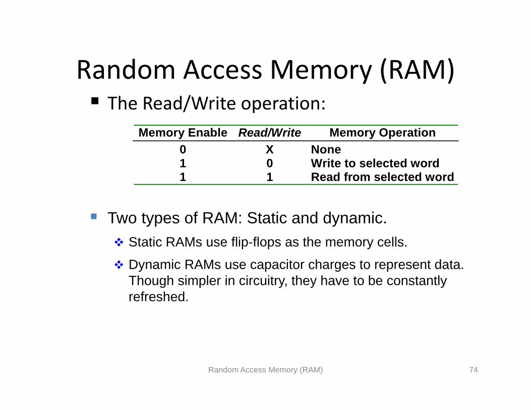
Random Access Memory (RAM)Random Access Memory (RAM) The Read/Write operation:
Memory Enable Read/Write Memory Operation0 X None1 0 Write to selected word1 1 Read from selected word1 1 Read from selected word
Two types of RAM: Static and dynamic. Static RAMs use flip-flops as the memory cells.
Dynamic RAMs use capacitor charges to represent data. Though simpler in circuitry they have to be constantlyThough simpler in circuitry, they have to be constantly refreshed.
Random Access Memory (RAM) 74

Random Access Memory (RAM)Random Access Memory (RAM) A single memory cell of the static RAM has
the following logic and block diagrams.g g g
Select
R
S QInput O t t BC O t tI t
Select
S QInput Output
Read/Write
BC OutputInput
Read/WriteRead/Write
Logic diagram Block diagram
Random Access Memory (RAM) 75

Random Access Memory (RAM)Random Access Memory (RAM) Logic construction of a 4 x 3 RAM (with
decoder and OR gates):
Random Access Memory (RAM) 76

Random Access Memory (RAM)Random Access Memory (RAM) An array of RAM chips: memory chips are
combined to form larger memory.combined to form larger memory.
A 1K x 8-bit RAM chip:
RAM 1K x 8
DATA (8)Input data (8) Output data8 810 ADRS (10)
CSRW
AddressChip selectRead/write
( ) p10
Block diagram of a 1K x 8 RAM chip
Random Access Memory (RAM) 77

Random Access Memory (RAM)Random Access Memory (RAM)
0–1023
Input data8 linesLines Lines
0 – 911 10
Address
1K x 8
DATA (8)ADRS (10)CSRW
(8)
1024 20470
2x4 decoder
0 911 10
S
1K x 8
DATA (8)ADRS (10)CSRW
(8)1024 – 20470
123
S0
S11
Lecture 15
Registers Counters Finite State Machine (FSM) design
1
Lecture 15
Registers Counters Finite State Machine (FSM) design
Read/write
1K x 8
DATA (8)ADRS (10)CSRW
(8)2048 – 3071
4K x 8 RAM.
RW
DATA (8)ADRS (10)CS
(8)
3072 – 4095
Random Access Memory (RAM) 78
Output data
1K x 8CSRW

Invalid States in countersInvalid States in counters
• Counter repeats 5 states in sequenceCounter repeats 5 states in sequence– Sequence is 000, 010, 011, 101, 110, 000
Step 1: State diagram Step 2: State transition tableAssume D flip-flopsPresent State Next State
000 110C B A C+ B+ A+
0 0 0 0 1 0
0 0 1 X X X010
011
1010 0 1 X X X
0 1 0 0 1 1
0 1 1 1 0 1
79
0111 0 0 X X X
1 0 1 1 1 0
1 1 0 0 0 0

3. Encode next state functions3. Encode next state functions
CC+ CB+ CA+C
A
0 0 0 X
C
A
1 1 0 X
C
A
0 1 0 X
X 1 X 0
B
AX 1 X 1
B
AX 0 X 1
B
X 1 X 0
A+ = BC'C+ = A B+ = B' + A'C'
80

4. Implement the design4. Implement the design
D Q D Q D QC B A
CLK
A
A'C'
BC'C
B'C'
Recall that a D flip flop also produces Q’ so A’, B’, and C’
81
p p p Q , ,
would all be available without any extra inverters

Is our design robust?Is our design robust?
• What if the counter starts in a 111 state?What if the counter starts in a 111 state?
001 111001
100
000 110
Does our counter get
stuck in invalid states???
010
011
101
82

5-state counter5 state counter
• Back-annotate our design to check itBack annotate our design to check it
Draw state diagramFill in state transition table
000 110C B A C+ B+ A+
0 0 0 0 1 0
Present State Next State 001
010 1010 0 1 1 1 0
0 1 0 0 1 1
0 1 1 1 0 1 0110 1 1 1 0 1
1 0 0 0 1 0
1 0 1 1 1 0
100
111A+ = BC'
83
1 1 0 0 0 0
1 1 1 1 0 0The proper methodology is to design your counter to be self-startingC+ = A
B+ = B' + A'C'

Self-starting countersSelf starting counters
• Invalid states should always transition to valid statesInvalid states should always transition to valid states– Assures startup
– Assures bit-error tolerance
• Design your counters to be self-starting– Draw all states in the state diagram
– Fill in the entire state-transition table
– May limit your ability to exploit don't cares• Choose startup transitions that minimize the logic
84