maharashtra state board of technical education (autonomous) (iso/iec...
TRANSCRIPT

MAHARASHTRA STATE BOARD OF TECHNICAL EDUCATION (Autonomous)
(ISO/IEC - 27001 - 2005 Certified)
Summer – 14 EXAMINATION Subject Code: 17333 Model Answer Page 1/ 27
Important Instructions to examiners:
1) The answers should be examined by key words and not as word-to-word as given in the
model answer scheme.
2) The model answer and the answer written by candidate may vary but the examiner may try
to assess the understanding level of the candidate.
3) The language errors such as grammatical, spelling errors should not be given more
Importance (Not applicable for subject English and Communication Skills.
4) While assessing figures, examiner may give credit for principal components indicated in the
figure. The figures drawn by candidate and model answer may vary. The examiner may give credit for any
equivalent figure drawn.
5) Credits may be given step wise for numerical problems. In some cases, the assumed constant
values may vary and there may be some difference in the candidate‟s answers and model answer.
6) In case of some questions credit may be given by judgement on part of examiner of relevant answer based
on candidate‟s understanding.
7) For programming language papers, credit may be given to any other program based on equivalent
concept.
1.
a) Attempt any six of the following:
i. State two advantages of digital system over analog system.
(Any 2 advantages 1 mark each)
1. They are less susceptible to noise.
2. The effect of fluctuation in the characteristic of the components, ageing of
components etc. is very small in digital circuits.
3. Digital circuits have capability of memory which makes them suitable for computers.
4. More accurate.
ii. Define with respect to digital ICs: (1 mark each)
1. Fan-in
The number of inputs of a logic gate can handle.
2. Noise immunity.
The circuit‟s ability to tolerate noise signals is referred to as noise immunity. It is
generally expressed in terms of high level and low level noise margins (expressed
in voltage)
iii. State any two Boolean laws. (Any 2 laws 1 mark each)
OR
Laws
AND
Laws
Associative Law Commutative
Law
Distributive Law
A+0=A A.1=A (A.B)C=A.(B.C) A.B=B.A A.B+A.C=A(B+C)
A+1=1 A.0=0 A+B=B+A (A+B)(A+C)=A+BC
A+A=A A.A=A
A+ =1 A. =1

MAHARASHTRA STATE BOARD OF TECHNICAL EDUCATION (Autonomous)
(ISO/IEC - 27001 - 2005 Certified)
Summer – 14 EXAMINATION Subject Code: 17333 Model Answer Page 2/ 27
iv. Draw symbol, logical expression and truth table of EX-OR gate.
A B Y
0 0 0
0 1 1
1 0 1
1 1 0
v. Convert (57)10 into binary equivalent.
2 57 1
2 28 0
2 14 0
2 7 1
2 3 1
2 1
(57)10=(111001)2
vi. Derive AND gate and OR gate using NAND gates only. (1 mark each)

MAHARASHTRA STATE BOARD OF TECHNICAL EDUCATION (Autonomous)
(ISO/IEC - 27001 - 2005 Certified)
Summer – 14 EXAMINATION Subject Code: 17333 Model Answer Page 3/ 27
vii. Draw the truth table of digital comparator IC7485.(2 marks)
(Correct function table should also be awarded complete marks)
Comparing inputs Cascading inputs Outputs
A3,B3 A2,B2 A1,B1 A0,B0 IA>B IA<B IA=B YA>B YA<B YA=B
A3>B3 X X X X X X H L L
A3<B3 X X X X X X L H L
A3=B3 A2>B2 X X X X X H L L
A3=B3 A2<B2 X X X X X L H L
A3=B3 A2=B2 A1>B1 X X X X H L L
A3=B3 A2=B2 A1<B1 X X X X L H L
A3=B3 A2=B2 A1=B1 A0>B0 X X X H L L
A3=B3 A2=B2 A1=B1 A0<B0 X X X L H L
A3=B3 A2=B2 A1=B1 A0=B0 H L L H L L
A3=B3 A2=B2 A1=B1 A0=B0 L H L L H L
A3=B3 A2=B2 A1=B1 A0=B0 L L L H H L
A3=B3 A2=B2 A1=B1 A0=B0 X X H L L H
A3=B3 A2=B2 A1=B1 A0=B0 H H L L L L
viii. Define the following specifications of A to D converter: (1 mark each)
i. Resolution
Resolution: Number of discrete value it can produce over the range of analog
values. OR
ADC resolution is no of bits used to represent analog input signal.
ii. Conversion time.
Referring to the below fig. At t=t0 a SOC signal is given to the ADC and at t=t1
we get EOC output.
The time difference between these two instants is called as “Conversion time”.
The conversion time should be as small as possible. Practically it can have value
from a few hundreds of S to a few msec.

MAHARASHTRA STATE BOARD OF TECHNICAL EDUCATION (Autonomous)
(ISO/IEC - 27001 - 2005 Certified)
Summer – 14 EXAMINATION Subject Code: 17333 Model Answer Page 4/ 27
b) Attempt any Two of the following:
i. Subtract using 1’s complement method (2 marks each)
1. (11011)2-(1010)2
2. (10111)2-(11000)2
ii. State and prove DeMorgan’s theorems. (2 marks each)
DeMorgan’s first theorem
Compliment of a product is equal to the sum of the compliment i.e.
A B A.B
0 0 1 1 0 1 1
0 1 1 0 0 1 1
1 0 0 1 0 1 1
1 1 0 0 1 0 0
Since the last 2 columns are same, theorem is proved.
DeMorgan’s second theorem
Compliment of a sum is equal to the product of compliments
A B A.B
0 0 1 1 0 1 1
0 1 1 0 1 0 0
1 0 0 1 1 0 0
1 1 0 0 1 0 0

MAHARASHTRA STATE BOARD OF TECHNICAL EDUCATION (Autonomous)
(ISO/IEC - 27001 - 2005 Certified)
Summer – 14 EXAMINATION Subject Code: 17333 Model Answer Page 5/ 27
Since the last two columns are same, theorem is proved.
iii. Convert the following: (1 mark each)
1. (11001)2=(?)10
2. (10101)2=(?)8
3. (37)8=(?)2

MAHARASHTRA STATE BOARD OF TECHNICAL EDUCATION (Autonomous)
(ISO/IEC - 27001 - 2005 Certified)
Summer – 14 EXAMINATION Subject Code: 17333 Model Answer Page 6/ 27
4. (5AC)=(?)2
2. Attempt any Four of the following:
a) Derive NOT gate and AND gate using NOR gates only. (2 marks each)

MAHARASHTRA STATE BOARD OF TECHNICAL EDUCATION (Autonomous)
(ISO/IEC - 27001 - 2005 Certified)
Summer – 14 EXAMINATION Subject Code: 17333 Model Answer Page 7/ 27
b) Simplify the following Boolean expressions using Boolean laws:
(2 marks each)
i.
ii.
c) Perform the following binary operations. (2 marks each)
i.
ii.

MAHARASHTRA STATE BOARD OF TECHNICAL EDUCATION (Autonomous)
(ISO/IEC - 27001 - 2005 Certified)
Summer – 14 EXAMINATION Subject Code: 17333 Model Answer Page 8/ 27
d) Design a half subtractor circuit using K-map.
(1 mark truth table, 1 mark K maps, 1 mark equations, 1 mark any one circuit
diagram)
e) Minimize the following Boolean expression using K-map.
Draw the logical diagram of minimized expression using logic gates.
(1 mark K map and grouping, 1 mark equation, 2 marks circuit diagram)

MAHARASHTRA STATE BOARD OF TECHNICAL EDUCATION (Autonomous)
(ISO/IEC - 27001 - 2005 Certified)
Summer – 14 EXAMINATION Subject Code: 17333 Model Answer Page 9/ 27
f) Draw the block diagram of octal to binary encoder and write its truth table.
(2 marks block diagram, 2 marks truth table)
3. Attempt any Four of the following:
a) Implement the logical expression using gates.
(Simplification 2 marks, circuit diagram 2 marks)

MAHARASHTRA STATE BOARD OF TECHNICAL EDUCATION (Autonomous)
(ISO/IEC - 27001 - 2005 Certified)
Summer – 14 EXAMINATION Subject Code: 17333 Model Answer Page 10/ 27
b) Draw logic diagram of 1:4 demultiplexer. Write truth table of it.
(Diagram 2M, truth table 2M)

MAHARASHTRA STATE BOARD OF TECHNICAL EDUCATION (Autonomous)
(ISO/IEC - 27001 - 2005 Certified)
Summer – 14 EXAMINATION Subject Code: 17333 Model Answer Page 11/ 27
c) Design 16:1 multiplexer using 4:1 multiplexers only.(4 Marks)
d) Convert the following Boolean expression into its standard forms: (2M each)
i.
ii.
e) What are the different triggering methods used in flip flop?(2 marks each)
Triggering is classified in to two types
1. Level Triggered
2. Edge Triggered
1. Level triggering:
The latch or flip-flop circuits which respond to their inputs, only if their enable input (E) or
clock input held at an active HIGH or LOW level are called as level triggered latches or flip
flops.
Positive level triggered:
If the outputs of S-R flip flop response to the input changes, for its clock input at high (1),
level then it is called as the positive level triggered S-R flip flop.

MAHARASHTRA STATE BOARD OF TECHNICAL EDUCATION (Autonomous)
(ISO/IEC - 27001 - 2005 Certified)
Summer – 14 EXAMINATION Subject Code: 17333 Model Answer Page 12/ 27
Negative level triggered FF:
If the outputs of an S-R flip-flop respond to the input changes, for its clock input at low(0)
level, then it is called as the negative level triggered S-R flip-flop.
2. Edge Triggering:
The flip-flop which changes their outputs only corresponding to the positive or negative edge
of the clock input are called as edge triggered flip-flops.
Types of edge triggered flip-flops:
There are two types of edge triggered flip flops:
Positive edge triggered flip flops: Positive edge triggered flip flops, will allow its outputs to
change only at the instants corresponding to the rising edges of clock(or positive spikes). Its
outputs will not respond to change in inputs at any other instant of time.
Negative edge triggered flip flops: Negative edge triggered flip-flops will respond only to
the going edges (or spikes) of the clock.
f) What is race around condition in JK flip flop and how it can be eliminated?(4 Marks)
For the racing around to take place, it is necessary to have the enable input high along
with J=K=1.
As the enable input remains high for a long time in a JK latch, the problem of multiple
toggling arises.
But in edge triggered JK flip flop, the positive clock pulse is present only for a very
short time.
Hence by the time the changed outputs return back to the inputs of NAND gates 3
and 4, the clock pulse has died down to zero. Hence the multiple toggling cannot take
place.
Thus the edge triggering avoids the race around condition.
4. Attempt any four of the following:
a) Draw the logical diagram of MOD-12 counters and describes is operation. Write its
truth table.(2M Diagram, 1M Description, 1M truth table)
(Any other correct circuit diagram should be awarded full marks)
Step 1: Write truth table:
For a MOD-12 counter, there will be 12 distinct states. We have to use 4 flip flops.

MAHARASHTRA STATE BOARD OF TECHNICAL EDUCATION (Autonomous)
(ISO/IEC - 27001 - 2005 Certified)
Summer – 14 EXAMINATION Subject Code: 17333 Model Answer Page 13/ 27
Note that output Y=0 for all the values of DCBA from 1100 i.e. 12 to 1111 i.e. 15
Step 2: K=Map for the output of the combination circuit is a shown in figure.
Simplifies expression is given by
Step 3: Draw the Circuit: (OR gate can be replaced by NAND gate. Inputs to NAND
gate will be C & D)
The MOD-12 counter is as shown in fig.
Step 4: Waveforms:

MAHARASHTRA STATE BOARD OF TECHNICAL EDUCATION (Autonomous)
(ISO/IEC - 27001 - 2005 Certified)
Summer – 14 EXAMINATION Subject Code: 17333 Model Answer Page 14/ 27
b) State any four specifications of A to D converter.(1 Mark each)
Analog input voltage: This is the maximum allowable input voltage range, 0–10 V, ± 5 V, ±
10 V, and so on.
Input impedance: Its value ranges from 1 kΩ to 1 MΩ depending upon the type of A/D
converter. Input capacitance is in the range of tens of pF.
Stability: The temperature dependence. Even if analog input is kept constant, the digital
output may change with temperature. This is called stability. It is expressed as % error per
degree rise in temperature.
Resolution is define as the maximum number of digital output codes. This is same as that of a
DAC
Resolution= 2n
Resolution is defined as the ratio of change in the value of the input analog voltage VA, required
to change the digital output by 1 LSB.
Resolution=
Conversion Time:
It is the total time required to convert the analog input signal into a corresponding digital
output.
As we know the conversion time depends on the conversion technique used for an ADC. The
conversion time is also dependent on the propagation delays introduced by the circuit
components.
Conversion time should ideally be zero and practically be as small as possible.
Quantization Error:
As shown in the figure the digital output is not always the accurate representation of
the analog input. For example any input voltage between1/8 to 2/8 of full scale will be
converted to a digital word of “001”
This approximation process is called as quantization and the error due to the
quantization process is called as quantization error.
The maximum value of quantization error is
The quantization error should be as small as possible. It can be reduce by increasing
the number of bits. The increase in number of bits will also improve the resolution.

MAHARASHTRA STATE BOARD OF TECHNICAL EDUCATION (Autonomous)
(ISO/IEC - 27001 - 2005 Certified)
Summer – 14 EXAMINATION Subject Code: 17333 Model Answer Page 15/ 27
c) Draw the logic circuit diagram of clocked SR flip flop using NAND gates. Write its truth
table.(Diagram 2M, Truth Table 2M)
(Either positive edge triggered or negative edge triggered flip flop should be
considered)
(Truth table with only for 4 conditions should also be awarded full marks)
The clocked SR flip flop is an edge triggered SR flip flop. It can be of two types.
1. Positive edge triggered
2. Negative edge triggered.
Positive edge triggered SR Flip Flop:
The positive edge triggered S-R flip Flop. It is also called as clocked SR FF.
This circuit will operate as an SR flip flop only for the positive clock edge but there is no
change in output id clock=0 or even for the negative going clock edge.
Operation:

MAHARASHTRA STATE BOARD OF TECHNICAL EDUCATION (Autonomous)
(ISO/IEC - 27001 - 2005 Certified)
Summer – 14 EXAMINATION Subject Code: 17333 Model Answer Page 16/ 27
Case I: S=X, R=X, clock=0
Since clock =0, the outputs of NAND gates 3 and 4 will be forced to be 1 irrespective
of the values of S and R. that means R‟= S‟=1 these are the inputs of the latch.
Hence the outputs of basic SR F/F i.e. Q and will not change in the output of the
clocked SR flip flop.
Case II: S=X, R=X, clock=1(high level)
As this flip flop does respond not respond to levels applied at the clock input, the outputs Q
and will not change. So
Case III: S= R=0: No Change
If S=R=0 then outputs of NND gates 3 and 4 are force to become 1.
Hence R‟ and S‟ both will be equal to 1. Since S‟ and R‟ are the inputs of the basic S-
R flip flop using NAND gates, there will be no change in the state of outputs.
Case IV: S=0 R=1,
Now S=0, R=1 and a positive edge is applied to the clock input.
Since S=0, output of NAND -3 i.e. R‟=1. And as R=1 and clock =1 the output of
NAND-4 i.e. S‟=0. Hence . This is the reset condition.
Case V: S=1 R=0,
Now S=1, R=0 and a positive going edge is applied to the clock input.
Output of NAND 3 i.e. R‟=0 and output of NAND 4 i.e. S‟ =1
Hence output of SR flip flop is
This is the reset condition.
Case VI: S=1 R=1,
As S=1, R=1 and clock=1, the outputs of NAND gates 3 and 4 both are 0. i.e.
S‟=R‟=0.
Hence the “Race” condition will occur in the basic SR flip-flop.
The symbol of positive edge triggered SR flip flop is as shown in figure and the truth
table.

MAHARASHTRA STATE BOARD OF TECHNICAL EDUCATION (Autonomous)
(ISO/IEC - 27001 - 2005 Certified)
Summer – 14 EXAMINATION Subject Code: 17333 Model Answer Page 17/ 27
Note that for clock input to be at negative or positive levels as the edge triggered flip
flop does not respond. Similarly it does not respond to negative edge of the clock.
The flip flop will respond only to the positive edge of clock.
With positive edge of the clock, the SR flip flop behaves in the following way:
Negative Edge Triggered S-R Flip Flop:
The internal circuit (with NAND gates) of the negative edge triggered S-R flip flop is
exactly same as that for the positive edge triggered one.
The differentiator circuit is slightly modified in order to enable the flip flop for the
negative (falling) edges of the clock input.
The circuit symbol of the negative edge triggered S-R flip flop and its truth table.
d) Explain the function of preset and clear terminals in JK flip flop. Write truth table of
it.(2M explanation ,2m Truth table)
A J-K flip flop with preset and clear inputs is shown in figure. These are the
synchronous preset and clear terminals.
Both these inputs are active low and have higher priority than all the other inputs.
J Q
K Q
PR
CLK
CLR

MAHARASHTRA STATE BOARD OF TECHNICAL EDUCATION (Autonomous)
(ISO/IEC - 27001 - 2005 Certified)
Summer – 14 EXAMINATION Subject Code: 17333 Model Answer Page 18/ 27
Inputs OUTPUT
Operation
performed CLK PR CLR
1 1 1 Qn+1 Normal JK
FF
X 0 1 1 FF is set
X 1 0 0 FF is reset
e) Classify memories. Compare RAM and Rom on two points.(2M classification, 2M
comparison).
RAM ROM
Volatile Memory Non Volatile Memory
Used as a temporary memory Used to store information such as lookup
tables fixed data etc.
f) Draw the circuit diagram of weighted resistor type D to A converter. Describe its
working.(Diagram 2M, Explanation 2M)
CONSTRUCTION and WORKING
1. This circuit uses a network of binary weighted resistors (i.e 21R, 2
2R… 2
nR) and a
summing amplifier.
2. There are ―n‖ number of electronic switches used, one per digital bit. They are single
pole double throw (SPDT) type switches.
3. The switch when connected to ground the input provided is ‗0„ while connected to
negative reference voltage (- VR) and when the binary input is ‗1„
4. Depending on the positions of various switches, the currents will start flowing through the
resistors 21R, 2
2R… 2
nR.
5. The op-amp is used as summing amplifier to convert the current to voltage
Let the n-bit digital input word to the DAC be d1d2. . . dn with d1 as MSB (most significant
bit) and dn as LSB (least significant bit).Let RF be the feedback resistor and Io be the output
current. Assume the Op-amp to be an ideal OP-AMP so that the current flowing between its
input terminals is zero.

MAHARASHTRA STATE BOARD OF TECHNICAL EDUCATION (Autonomous)
(ISO/IEC - 27001 - 2005 Certified)
Summer – 14 EXAMINATION Subject Code: 17333 Model Answer Page 19/ 27
The output current Io is the sum of individual currents through the weighted resistors.
The output voltage Vo is given by,
This is the required expression for output voltage.
Let the 3-bit digital input word to the DAC be d1d2d3.d1 is the MSB and d3 is the LSB.
Vo= VR [ d1 2-1
+ d22-2
+ d 32-3
]
5. Attempt any Four of the following:
a) Perform the following BCD addition (2 marks each)
i) (65)10 + (52)10
65 0110 0101
+
52 0101 0010
____________________
1011 0111
+
0110
_____________________
1 0001 0111
(1 1 7)10

MAHARASHTRA STATE BOARD OF TECHNICAL EDUCATION (Autonomous)
(ISO/IEC - 27001 - 2005 Certified)
Summer – 14 EXAMINATION Subject Code: 17333 Model Answer Page 20/ 27
ii) (74)10 - (36)10
74 0111 0100
-
36 0011 0110
______________________
0011 1110
-
0110
______________________
0011 1000
(3 8)10
b) D type flip flop using NAND gates (2 marks for diagram, 2 marks for truth table)
Truth Table
Input
Dn
Output
Q
0 1
1 0
c) Design a circuit using basic logic gates to realize the following function. (4 marks)

MAHARASHTRA STATE BOARD OF TECHNICAL EDUCATION (Autonomous)
(ISO/IEC - 27001 - 2005 Certified)
Summer – 14 EXAMINATION Subject Code: 17333 Model Answer Page 21/ 27
d) Draw the logical circuit diagram of 3 bit asynchronous up counter and describe its
operation. (2 marks diagram, 2 marks working)
A 3 bit asynchronous up counter requires 3 flip flops FF0, FF!, FF2. Q2, Q1, Q0 are the
outputs of these flip flops. The output Q0 of the least significant flip flop, changes for every
clock pulse. This is achieved by using T type flip flop with T0 = 1. Q0 is connected to clock
input of the next flip flop. The output Q1 makes the transition (from 0 to 1 or 1 to 0)
whenever Q0 changes from 1 to 0. Q1 is connected to clock input of the next flip flop (most
significant flip flop). The output Q2 makes the transition (from 0 to 1 or 1 to 0) whenever Q1
changes from 1 to 0.
e) Draw the Block diagram of BCD to seven segment decoder using IC 7447. Write the
truth table of it.(2 marks diagram, 2 marks Truth Table
Truth Table of BCD to seven segment decoder
Decimal Inputs Outputs
B3 B2 B1 B0 a b c d e f g
0 0 0 0 0 0 0 0 0 0 0 1
1 0 0 0 1 1 0 0 1 1 1 1
2 0 0 1 0 0 0 1 0 0 1 0
3 0 0 1 1 0 0 0 0 1 1 0
4 0 1 0 0 1 0 0 1 1 0 0
5 0 1 0 1 0 1 0 0 1 0 0
6 0 1 1 0 0 1 0 0 0 0 0
MAHARASHTRA STATE BOARD OF TECHNICAL EDUCATION (Autonomous)
(ISO/IEC - 27001 - 2005 Certified)
Summer – 14 EXAMINATION Subject Code: 17333 Model Answer Page 22/ 27
7 0 1 1 1 0 0 0 1 1 1 1
8 1 0 0 0 0 0 0 0 0 0 0
9 1 0 0 1 0 0 0 0 1 0 0
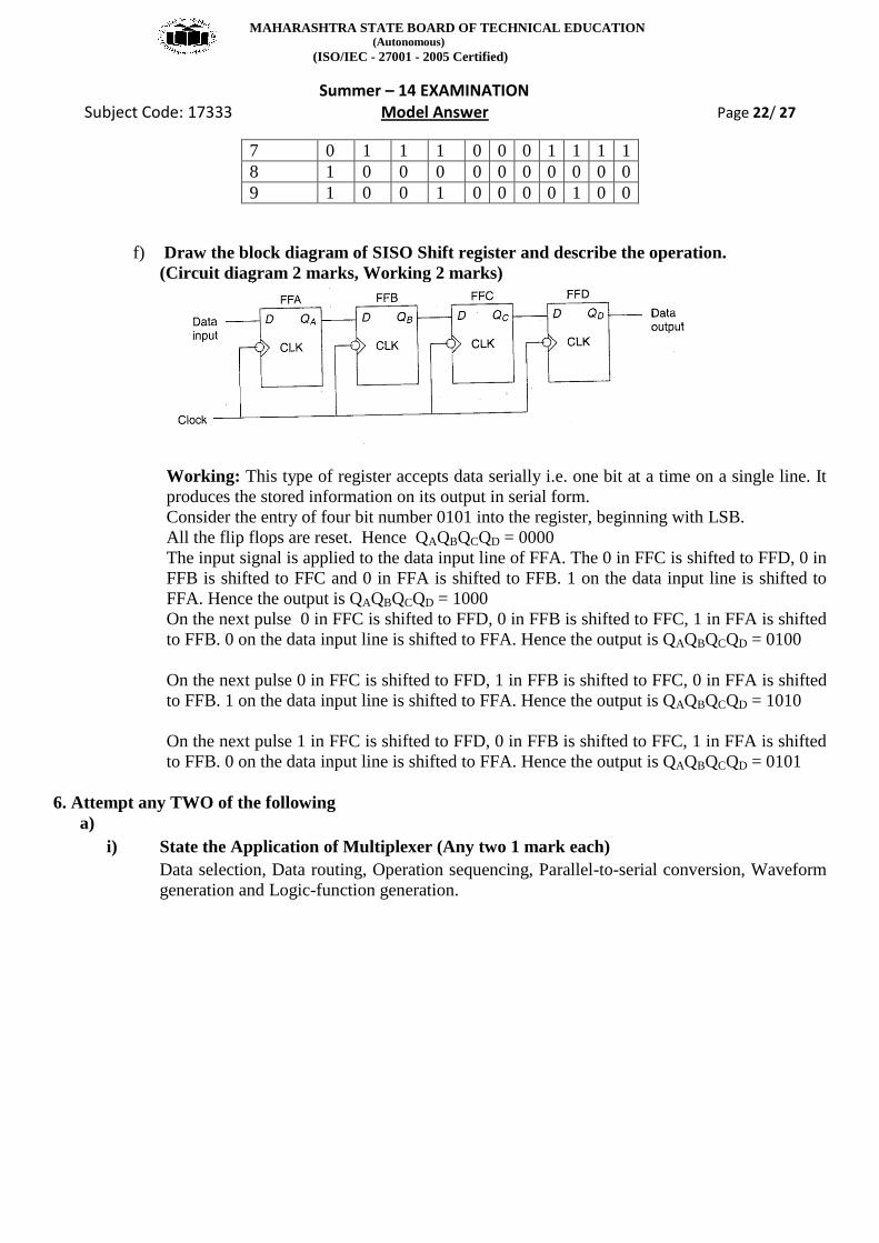
f) Draw the block diagram of SISO Shift register and describe the operation.
(Circuit diagram 2 marks, Working 2 marks)
Working: This type of register accepts data serially i.e. one bit at a time on a single line. It
produces the stored information on its output in serial form.
Consider the entry of four bit number 0101 into the register, beginning with LSB.
All the flip flops are reset. Hence QAQBQCQD = 0000
The input signal is applied to the data input line of FFA. The 0 in FFC is shifted to FFD, 0 in
FFB is shifted to FFC and 0 in FFA is shifted to FFB. 1 on the data input line is shifted to
FFA. Hence the output is QAQBQCQD = 1000
On the next pulse 0 in FFC is shifted to FFD, 0 in FFB is shifted to FFC, 1 in FFA is shifted
to FFB. 0 on the data input line is shifted to FFA. Hence the output is QAQBQCQD = 0100
On the next pulse 0 in FFC is shifted to FFD, 1 in FFB is shifted to FFC, 0 in FFA is shifted
to FFB. 1 on the data input line is shifted to FFA. Hence the output is QAQBQCQD = 1010
On the next pulse 1 in FFC is shifted to FFD, 0 in FFB is shifted to FFC, 1 in FFA is shifted
to FFB. 0 on the data input line is shifted to FFA. Hence the output is QAQBQCQD = 0101
6. Attempt any TWO of the following
a)
i) State the Application of Multiplexer (Any two 1 mark each)
Data selection, Data routing, Operation sequencing, Parallel-to-serial conversion, Waveform
generation and Logic-function generation.

MAHARASHTRA STATE BOARD OF TECHNICAL EDUCATION (Autonomous)
(ISO/IEC - 27001 - 2005 Certified)
Summer – 14 EXAMINATION Subject Code: 17333 Model Answer Page 23/ 27
ii) Design Full Adder using K maps and circuit diagram using Logic gates
(2 marks for truth table, 2 marks for K maps, 2 marks for circuit diagram using logic
gates)
(Any correct circuit diagram using logic gates should awarded marks)
Truth Table
Inputs Outputs
An Bn Cn-1 Sn Cn
0 0 0 0 0
0 0 1 1 0
0 1 0 1 0
0 1 1 0 1
1 0 0 1 0
1 0 1 0 1
1 1 0 0 1
1 1 1 1 1
K Maps
K map for Sum k map for Carry
Equation foe Sum ande Carry
Circuit Diagram

MAHARASHTRA STATE BOARD OF TECHNICAL EDUCATION (Autonomous)
(ISO/IEC - 27001 - 2005 Certified)
Summer – 14 EXAMINATION Subject Code: 17333 Model Answer Page 24/ 27
Circuit Diagram for Sum Circuit diagram for Carry
b)
i) Compare Combinational and sequential logic circuits on two points.(Any two points 1
mark each)
Combinational Circuits Sequential Circuits
Output depends on inputs present at that
time
Output depends on present inputs and past inputs/
outputs
Memory is not necessary Memory is necessary
Clock input is not necessary Clock input is necessary
For e.g. Adders, Subtractors For e.g. Shift registers, Counters
ii) State the applications of shift registers (Any two 1 mark each)
1. Delay line
2. Serial to parallel converter
3. Parallel to serial converter
4. Ring counter
5. Twisted Ring counter
6. Sequence generator

MAHARASHTRA STATE BOARD OF TECHNICAL EDUCATION (Autonomous)
(ISO/IEC - 27001 - 2005 Certified)
Summer – 14 EXAMINATION Subject Code: 17333 Model Answer Page 25/ 27
iii) Block diagram of 4 bit PIPO shift register (Block Diagram 1 mark, Working 1 mark,
Truth table 1 mark, Timing Diagram 1 mark) (Any correct block diagram with
working should awarded marks)
Block diagram
Working: In Parallel In-Parallel out Shift register, the data bits are entered simultaneously into their
respective stages on parallel lines. The output data bits are also available on parallel lines.
Immediately following the simultaneous entry of all data bits, the bits appear in the parallel outputs.
Truth Table
Inputs Outputs
ABCD QA QB Qc QD
1111 1 1 1 1
Timing diagram

MAHARASHTRA STATE BOARD OF TECHNICAL EDUCATION (Autonomous)
(ISO/IEC - 27001 - 2005 Certified)
Summer – 14 EXAMINATION Subject Code: 17333 Model Answer Page 26/ 27
c)
i) Draw the circuit diagram of Successive approximation type A to D converter and describe
its working. (Circuit Diagram 2 marks, Working 2 Marks)
Block diagram
Working: The comparator serves the function of the scale, the output of which is used for
setting/ resetting the bits at the output of the programmer. This output is converted into
equivalent analog voltage from which offset is subtracted and then applied to the inverting
input terminal of the comparator. The outputs of the programmer will change only when the
clock pulse is present.
To start the conversion, the programmer sets the MSB to 1 and all other bits to 0. This is
converted into analog voltage by the DAC and the comparator compares it with the analog
input voltage. If the analog input voltage Va >= Vi, the output voltage of the comparator is
HIGH, which sets the next bit also. On the other hand if Va <= Vi, Then the output of the
comparator is LOW which resets the MSB and sets the next bit. Thus a 1 is tried in each bit
of DAC until the binary equivalent of analog input voltage is obtained.
ii) A D to A converter has a full scale analog output of 12V with 4 binary inputs. Find the
voltage corresponding to each analog step. (Formula 1 mark, Output Voltages 3 marks)
Ans:
Formula
Vo = Full scale analog output/2n-1
= 12/24-1
= 12/15
= 0.8

MAHARASHTRA STATE BOARD OF TECHNICAL EDUCATION (Autonomous)
(ISO/IEC - 27001 - 2005 Certified)
Summer – 14 EXAMINATION Subject Code: 17333 Model Answer Page 27/ 27
Inputs Output
D C B A Vo in Volts
0 0 0 0 0
0 0 0 1 0.8
0 0 1 0 1.6
0 0 1 1 2.4
0 1 0 0 3.2
0 1 0 1 4
0 1 1 0 4.8
0 1 1 1 5.6
1 0 0 0 6.4
1 0 0 1 7.2
1 0 1 0 8
1 0 1 1 8.8
1 1 0 0 9.6
1 1 0 1 10.4
1 1 1 0 11.2
1 1 1 1 12