magnetic thin films with graded or tilted anisotropy for spintronic devices
TRANSCRIPT
THESIS FOR DEGREE OF DOCTOR OF PHILOSOPHY
Magnetic Thin Films with Graded or Tilted
Anisotropy for Spintronic Devices
YEYU FANG
Department of Physics
University of Gothenburg
SE-412 96 Gothenburg, Sweden 2013
©Yeyu Fang, 2013
ISBN: 978-91-628-8705-6
Link: http://hdl.handle.net/2077/32729
Applied Spintronic Group,
Department of Physics,
University of Gothenburg,
SE-412 96 Gothenburg, Sweden
Printed by Kompendiet
Gothenburg, Sweden 2013
i
Abstract
In this thesis magnetic thin films with graded or tilted anisotropy are intensively studied for potential applications in spintronic devices.
A continuum of stable remanent resistance states is realized in Co/Pd multilayers based on a perpendicularly magnetized pseudo spin valve (PSV). The Co/Pd multilayers have been deposited using magnetron sputtering. By varying the Co thickness in each repeating unit, a graded anisotropy through the multilayer is achieved. We then incorporate this graded Co/Pd multilayer into a PSV as the free layer. The remanent resistance states are systematically adjustable depending on the reversal field. The gradual reversal of the free layer with applied field and the field-independent fixed layer leads to a range of stable and reproducible remanent resistance values, as determined by the giant magnetoresistance of the device. An analysis of first-order reversal curves (FORCs) combined with magnetic force microscopy (MFM) shows that the origin of the effect is the field-dependent population of up and down domains in the free layer. Thus, these structures have great potential for applications such as field-tunable resistance trimming devices, memristive devices, or magnetic analog memories with a continuous number of states per memory cell, thereby allowing much higher information storage.
We have also successfully realized FePtCu thin films with graded anisotropy. During deposition a compositional gradient is achieved by continuously varying the Cu content from the top to bottom. After annealing at a proper temperature, the top Cu-poor regions remain in the as-deposited soft A1 phase, while the bottom Cu-rich regions transform into hard L10 phase. Hence the gradient anisotropy is established through the film thickness. The critical role of the annealing temperatures (TA) on the resultant anisotropy gradient is investigated. Magnetic measurements support the creation of an anisotropy gradient in properly annealed films which exhibit both a reduced coercivity and moderate thermal stability. The reversal mechanism of graded anisotropy has been investigated by alternating gradient magnetometer (AGM) and magneto optical Kerr effect (MOKE) measurements in combination with the FORC technique. The AGM-FORC analysis clearly shows the soft and hard phases. MOKE-FORC measurement, which preferentially probes the surface of the film, reveals that the soft components are indeed located toward the top surface. We provide a detailed study of the how the anisotropy gradient in a compositional graded FePtCu film gradually develops as a function of the TA. By utilizing the in-situ annealing and magnetic characterization capability of a physical property measurement system (PPMS), the evolution of the induced anisotropy gradient is elucidated. These results are important and useful for the solving the magnetic ‘‘trilemma’’ of magnetic recording technology.
The Co/Pd-NiFe exchange spring system is investigated. Due to the competition between the strong perpendicular anisotropy of the Co/Pd multilayer and the in-plane shape anisotropy of the NiFe, the magnetization in the NiFe tilts out of the film plane. Experimental data from conventional magnetometry, MFM, and ferromagnetic resonance (FMR), along with one-dimensional simulations, show that the titling angle in the NiFe layer is highly tunable from 0 to 60° by simply changing the thickness of NiFe. We employed the Co/Pd-NiFe exchange spring system with appropriate NiFe thickness as the polarizer in nano-contact spin torque oscillators (STOs) which show vortex oscillations at low fields.

ii
Acknowledgements
I completed the first part of my PhD at the Royal Institute of Technology (KTH),
Sweden. I finished my Licentiate thesis there and then moved to University of Gothenburg
(GU) to continue my PhD study with Professor Johan Åkerman.
First and foremost I would like to thank my advisor, Professor Johan Åkerman, for his
excellent supervision and professional guidance. In addition to his scientific knowledge, I
have also learned a lot from him on the personal level, such as how to deal with problems in
life, how to work efficiently, and how to use a humorous attitude to face tough situations. A
special thanks to my co-supervisor at GU, Dr. Randy K. Dumas, for practically working with
me in the lab with endless patience to my questions,constant encouragement, and fruitful
discussions which have led to numerous papers.
I am also deeply grateful to Professor Mattias Goksör, current director of the Physics
Department at GU, for leading a great department. I also would like to express my gratitude to
Professor Ulf Karlsson, head of the Research Unit and my co-supervisor at KTH, and
Professor Oscar Tjernberg, current head of the Materials Physics Department at KTH, for
doing your best to keep up a creative and active environment to work in. I am also thankful to
my examiner at GU, Professor Mats Jonson for endless patience and guidance in regards to
my study plan.
I always felt at home when stepping onto the eighth floor. I should also thank the
friendly colleagues in Physics Department at GU, especially Prof. Dag Hanstorp, Prof. Klavs
Hansen and Dr. Annette Granéli for arranging social activities.
I would like to express my sincere gratitude to the collaborators who I worked with,
Dr. Casey W. Miller, Dr. Chaolin Zha, Dr. Valentina Bonnani and Dr. Nguyen T. N. Anh,
iii
who shared their knowledge of science and life. A big thanks also goes out to the graduate
students who preceded me, Dr. Yan Zhou, Dr. Stefano Bonetti, and Dr. Majid Mohseni, who
set exceptional examples.
This thesis could not have been finished without support from our current
administrators Johanna Gustavsson and Bea Augustsson. Thank you so much for your
excellent work. And I also want to thank my previous administrators in KTH, Madeleine
Printzsköld and Marianne Widing, who helped me in my first three years regarding
administrative issues at KTH.
I am indebted to many other colleagues in our group, Johan Persson, Sohrab R. Sani,
Fredrik Magnusson, Dr. Pranaba Muduli, Dr. Yevgen Pogoryelov, Dr. Nadjib Benatmane,
Ezio Iacocca, Anders Eklund, Philipp Dürrenfeld, Tuan Le, and Fatjon Qejvanaj. Additionally,
all the colleagues and professors working in the other groups at the Physics department (GU)
and Material Physics department (KTH) deserve my deep appreciations. I am grateful to you
all for creating such a nice and international working atmosphere.
Thanks a lot to all the friends in Gothenburg and Stockholm who give me the happy
memories. In particular, Minshu Xie, Chen Hu, Sha Tao, and Jia Mao, with whom I spent
most of spare time with, you all deserve a very special thanks on a personal level. Thank you
so much.
Last, but not least, this thesis is dedicated to my parents and my sister. Loving you
from my deep inside.
Yeyu Fang
Gothenburg, April, 2013
iv
Research Publications
This thesis is partly based on the work contained in the following papers, printed as appendices and referred to by capital roman numerals in the text.
I. Yeyu Fang, R.K. Dumas, T. N. Anh Nguyen, M. Mohseni, S. Chung, and Johan Åkerman,
‘‘A non-volatile spintronic memory element with a continuum of resistance states ’’,
Advanced Functional Materials, 23, 1919 (2013)
II. C. L. Zha, R. K. Dumas, Y. Y. Fang, V. Bonanni, J. Nogués, and Johan Åkerman,
‘‘Continuously graded anisotropy in single (Fe53Pt47)100-xCux films ’’,
Applied Physics Letters, 97, 182504 (2010)
III. V. Bonanni, Y. Y. Fang, R. K. Dumas, C. L. Zha, S. Bonetti, J. Nogués, and Johan Åkerman,
‘‘First order reversal curve analysis of graded anisotropy FePtCu films ’’,
Applied Physics Letters, 97, 202501 (2010).
IV. Yeyu Fang, R. K. Dumas, C. L. Zha, and Johan Åkerman,
‘‘An in-situ anneal study of graded anisotropy FePtCu thin films’’,
IEEE Magnetics Letters, 2, 5500104 (2011).
V. T. N. Anh Nguyen, Y. Fang, V. Fallahi, N. Benatmane, M. Mohseni, R.K. Dumas, and Johan Åkerman,
‘‘[Co/Pd]-NiFe exchange springs with tunable magnetization tilt angle’’,
Applied Physics Letters, 98, 172502 (2011).
The contributions by the author, Yeyu Fang, to these papers were the following:
I. I was responsible for the sample deposition and measurements used in the publication. I analyzed the data and wrote the first draft of the manuscript, then worked on it with the other co-authors.
II. I partially participated in the sample deposition and was responsible for the alternating gradient magnetometer (AGM) measurements. I also contributed to the analysis of the major hysteresis loops.
III. I was responsible for the alternating gradient magnetometer (AGM) measurements used in this manuscript. I initially analyzed all the first-order reversal curves (FORCs).
v
IV. I was responsible for all the measurements used in this paper and performed data analysis. I wrote the first draft of the manuscript, and then worked on it with the other co-authors.
V. I measured the AGM major hysteresis loops and magnetic force microscope (MFM) images of all the samples. And I was also responsible for the analysis of those data.
Papers not included in the thesis:
1. C. L. Zha, Y. Y. Fang, J. Nogués, and Johan Åkerman, “Improved magnetoresistance through spacer thickness optimization in tilted pseudo spin valves based on L10 (111)-oriented FePtCu fixed layers”, Journal of Applied Physics, 106, 053909 (2009). 2. C. L. Zha, J. Persson, S. Bonetti, Y. Y. Fang, and Johan Åkerman , “Pseudo spin valves based on L10 (111)-oriented FePt fixed layer with tilted anisotropy”, Applied Physics Letters, 94, 163108 (2009). 3. Y. Y. Fang, C. L. Zha, S. Bonetti, and Johan Åkerman , “FORC studies of exchange biased NiFe in L10(111) FePt-based spin valve”, Journal of Physics:Conference Series, 200, 072002 (2010). 4. R. K. Dumas, C.L. Zha, Y. Y. Fang, V. Bonanni, J. W. Lau, J. Nogués, and Johan Åkerman, “Graded Anisotropy FePtCu films”,
IEEE Transactions on Magnetics, 47,1580 (2011). 5. R. K. Dumas, Yeyu Fang, B. J. Kirby, C. L. Zha, V. Bonanni, J. Nogués, and Johan Åkerman,
“Probing vertically graded anisotropy in FePtCu thin films”,
Physical Review B, 84, 054434 (2011)
6. S. M. Mohseni, R. K. Dumas, Y. Fang, J. W. Lau, S. R. Sani, J. Persson, and Johan Åkerman,
“Temperature-dependent interlayer coupling in Ni/Co perpendicular pseudo-spin-valve structures”,
Physical Review B, 84, 174432 (2011).
vi
7. Yeyu Fang, J. Persson, C. Zha, J. Willman, C. Hendryx, Casey W. Miller, and Johan Åkerman,
“Utility of reactively sputtered CuNx films in spintronics devices”,
Journal of Applied Physics, 111, 073912 (2012).
8. T. N. AnhNguyen, N. Benatmane, V. Fallahi, Yeyu Fang, S. M. Mohseni, R. K. Dumas, Johan Åkerman,
“[Co/Pd]4-Co-Pd-NiFe exchange springs with highly tuned/uniform magnetization tilt angles”,
Journal of Magnetism and Magnetic Materials, 324, 3929(2012)
*Part of the thesis is from my licentiate thesis: Tilted and graded anisotropy FePt and FePtCu thin
films for the application of hard disk drive and spin torque oscillators
Link: http://urn.kb.se/resolve?urn=urn:nbn:se:kth:diva-34013
ISBN: 978-91-7415-996-7
Table of Contents
Chapter 1 Introduction ......................................................................................................................... 1
1.1 Background ................................................................................................................................... 1
1.1.1 Spintronics .............................................................................................................................. 1
1.1.2 Magnetic anisotropy ............................................................................................................... 6
1.2 Motivation ..................................................................................................................................... 9
1.2.1 To increase the magnetic storage capacity: a non-volatile multi-level spintronics memory element ............................................................................................................................................ 9
1.2.2 A possible solution to the magnetic recording trilemma: magnetic media with graded anisotropy ........................................................................................................................................ 9
1.2.3 To remove the magnetic field requirement for spin torque oscillators: spin polarizer with tilted anisotropy ............................................................................................................................. 12
Chapter 2 Experimental methods ...................................................................................................... 15
2.1 Fabrication techniques ................................................................................................................. 15
2.1.1 Magnetron sputtering............................................................................................................ 15
2.1.2 Fabrication of nano-contact STOs ........................................................................................ 18
2.2 Structural characterization techniques ......................................................................................... 19
2.2.1 X-Ray Diffractometer ........................................................................................................... 19
2.2.2 X-Ray Diffraction (XRD) ..................................................................................................... 21
2.2.3 X-Ray Reflectivity (XRR) .................................................................................................... 22
2.2.4 Atomic Force Microscopy (AFM) ........................................................................................ 24
2.3 Magnetic properties characterization techniques ........................................................................ 29
2.3.1 Magnetic Force Microscopy (MFM) .................................................................................... 29
2.3.2 Vibrating Sample Magnetometer (VSM) ............................................................................. 29
2.3.3 Physical Property Measurement System (PPMS)-VSM ...................................................... 31
2.3.4 Alternating Gradient Magnetometer (AGM) ........................................................................ 33
2.3.5 Magneto-Optical Kerr Effect (MOKE) ................................................................................ 34
2.3.6 First-Order Reversal Curve (FORC) technique .................................................................... 37
2.4 Transport measurements .............................................................................................................. 40
2.4.1 DC characterization (Four probe measurement) .................................................................. 40
2.4.2 High frequency measurement setup ..................................................................................... 41
Chapter 3 Results and discussions ..................................................................................................... 43
3.1 Non-volatile spintronics element with continuous different resistance levels (Paper I) ............. 43
3.2 Solution for magnetic recording trilemma: graded anisotropy FePtCu ....................................... 48

3.2.1 Continuously graded anisotropy in single FePtCu thin films (Paper II) .............................. 48
3.2.2 First-order reversal curve analysis of graded anisotropy FePtCu films (Paper III) .............. 53
3.2.3 An in-situ anneal study of graded anisotropy FePtCu films (Paper IV) ............................... 59
3.3 Solution for the STO applied field problem: tilted polarizer (Paper V) ...................................... 64
Chapter 4 Conclusions and future works .......................................................................................... 70
Bibliography ........................................................................................................................................ 72
List of Figures ...................................................................................................................................... 77

1
Chapter 1 Introduction
1.1 Background
1.1.1 Spintronics
Electrons have a charge and a spin, but most conventional electronic devices only
exploit the electron charge in the conduction mechanics while ignoring the spin degree of
freedom. Spintronics (often synonymous with magneto-electronics) is a technique which
studies and utilizes the both the electronic charge and spin of the electrons. Taking advantage
of the spin degree of freedom opens the door for numerous interesting phenomena, novel
functionalities, and new devices.
The discovery of giant magnetoresistance (GMR) is considered the milestone in the
development of spintronics, which consequently resulted in intensive research on magnetic
materials and magnetic thin films. The first generation spintronic devices were the read heads
of hard disk drives (HDDs). In 2007, Peter Grünberg and Albert Fert were awarded the
Nobel Prize for their discovery of GMR in Fe/Cr/Fe trilayers1 and (Fe/Cr) multilayers2,
respectively.
Ferromagnetic metals, e.g. Fe, Co, and Ni, unlike normal metals, have a splitting of
spin-up and spin down states at the Fermi level in the band structure, as shown in Fig.1.1(a),
thereby allowing different conduction properties of each spin channel. The electrons in
conduction band sometimes can be polarized: there are more spins tending to point in one
direction than the other one. Therefore such magnetic materials can act as spin-polarizers. If a
current is passed through two magnetic layers placed next to each other, the incoming
unpolarized electrons go through the first magnetic layer and are preferentially polarized in
2
the direction of the magnetization of that layer upon transmission. The resistance through a
stack of magnetic layers depends on the relative density of states of the majority spin-carriers
at the Fermi level between the magnetic layers. In the other words, the stack encounters a
low-resistance if the magnetizations of the two ferromagnetic layers are parallel and a high-
resistance if the magnetizations of the two layers are anti-parallel. The difference between the
low-resistance and high-resistance states can be a few tens of percent 3 for spin-valves (two
ferromagnetic layers separated by a conductive non-magnetic spacer, e.g. Cu) or several
hundreds of percent4,5 for magnetic tunnel junctions (magnetic layers separated by an
insulating barrier such as MgO or Al2O3).
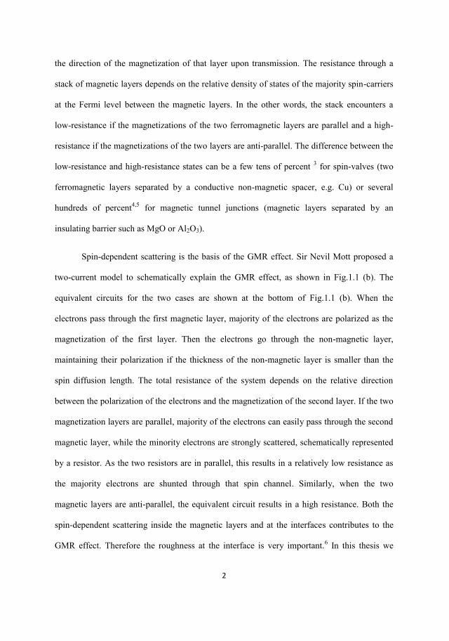
Spin-dependent scattering is the basis of the GMR effect. Sir Nevil Mott proposed a
two-current model to schematically explain the GMR effect, as shown in Fig.1.1 (b). The
equivalent circuits for the two cases are shown at the bottom of Fig.1.1 (b). When the
electrons pass through the first magnetic layer, majority of the electrons are polarized as the
magnetization of the first layer. Then the electrons go through the non-magnetic layer,
maintaining their polarization if the thickness of the non-magnetic layer is smaller than the
spin diffusion length. The total resistance of the system depends on the relative direction
between the polarization of the electrons and the magnetization of the second layer. If the two
magnetization layers are parallel, majority of the electrons can easily pass through the second
magnetic layer, while the minority electrons are strongly scattered, schematically represented
by a resistor. As the two resistors are in parallel, this results in a relatively low resistance as
the majority electrons are shunted through that spin channel. Similarly, when the two
magnetic layers are anti-parallel, the equivalent circuit results in a high resistance. Both the
spin-dependent scattering inside the magnetic layers and at the interfaces contributes to the
GMR effect. Therefore the roughness at the interface is very important.6 In this thesis we
3
utilized both atomic force microscopy (AFM) and X-ray reflectivity (XRR) to directly and
indirectly determine the roughness.
Figure 1.1 (a) Schematic band structure of a ferromagnetic metal showing the energy band spin splitting. (b) Explanation of the GMR effect: spin-dependent electron scattering and
redistribution of scattering events upon antialignment of magnetizations. Black arrows are the magnetizations of the ferromagnetic layers.
The second generation of spintronics research has been focused on the spin-transfer
torque (STT) effect, which was predicted by John Slonczewski9 and Luc Berger.10 When an
electron current passes through one magnetic layer, the electrons become preferentially spin
polarized, and when these polarized electrons transport to another magnetic layer, due to
conservation of the angular momentum, the polarized electrons can transfer angular
momentum, thereby exerting a torque on the magnetization of another magnetic layer. Under
the correct conditions STT can either change the orientation of or promote stable oscillations,
typically in the microwave frequency range, of the magnetization. This effect has rapidly
gained tremendous interests from scientists and researchers not only from the fundamental
point of view, but also the immediate applications to second generation spintronics devices.
Two main applications are STT-magnetic random access memory (STT-MRAM) and spin
torque oscillators (STOs).
4
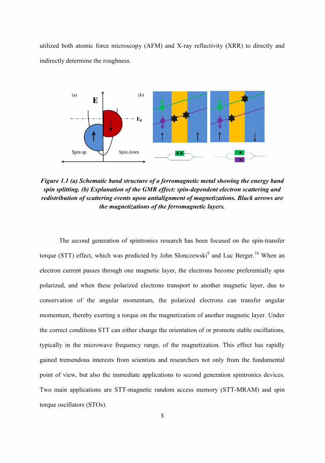
Fig.1.2 schematically shows the basic STT mechanism. In macroscopic theory, the
ferromagnet is treated as one magnetization vector . The equation of motion of a magnetic
moment under the applied magnetic field is summarized as Landau–Lifshitz–Gilbert (LLG)
equation
| |
Where is the magnetization vector, is the gyromagnetic ratio, =
, and is the
Gilbert damping constant which represents all the dissipative relaxation mechanisms. The
effective field is the negative gradient of the free energy density with respect to the
magnetization
( )
The Zeeman energy term , and the demagnetization energy terms
are magnetostatic in origin, the anisotropy energy from the crystalline or interfacial energies,
and the well-known exchange energy due to spin-dependent quantum mechanical interactions.
In this case, we assume that the exchange energy is strong enough to ensure that the entire
spins move together as one “macrospin”. As illustrated in Fig.1.2, when an external magnetic
field is applied, generates a torque in the form of which causes the magnetic
moment to precess around the effective field. However the magnetic moment is not able to
freely precess forever and the damping term, proportional to
, pushes the magnetic
moment to eventually relax along Heff.
Slonczweski proposed that an extra term should be added to the LLG equation to form
the LLG-S equation:
5
| |
| |
,
the last term is the Slonczweski spin torque term with the magnitude of
is the magnetization of the free layer, is the magnetization of the fixed layer,
is the angle between and , is the current density, d is the free layer thickness, and
, where are all material dependent parameters.11
Depending on the current density, there are two behaviors that the free layer can
realize. If the current density is large enough the Slonczweski spin torque term can
compensate the dissipative Gilbert damping term and the free layer will undergo a steady
precession. If the current density goes even higher, the spin torque term can be large enough
to completely switch the magnetization direction of the free layer.
Figure 1.2. Illustrantion of the magnetization precession.
6
1.1.2 Magnetic anisotropy
Ferromagnetic materials show directional dependence of magnetic properties, e. g. the
energy required to magnetize a ferromagnetic crystal depends on the direction of the applied
magnetic field with respect to the crystal axes. The physical basis that underlies a preferred
magnetic moment orientation in ultrathin magnetic films and multilayers can be quite
different from the factors that account for the easy-axis alignment along a symmetry direction
of a bulk material, and the strength can also be markedly different.12 This magnetic anisotropy
plays key roles in this thesis. Furthermore, from both the fundamental and applied points of
view, magnetic anisotropy is one of the most important properties of magnetic materials.
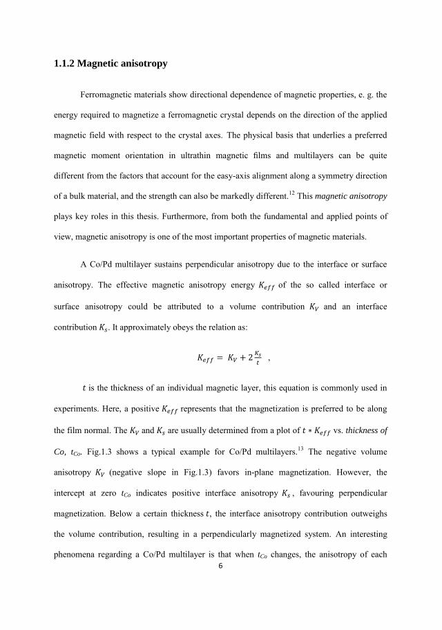
A Co/Pd multilayer sustains perpendicular anisotropy due to the interface or surface
anisotropy. The effective magnetic anisotropy energy of the so called interface or
surface anisotropy could be attributed to a volume contribution and an interface
contribution . It approximately obeys the relation as:
,
is the thickness of an individual magnetic layer, this equation is commonly used in
experiments. Here, a positive represents that the magnetization is preferred to be along
the film normal. The and are usually determined from a plot of vs. thickness of
Co, tCo. Fig.1.3 shows a typical example for Co/Pd multilayers.13 The negative volume
anisotropy (negative slope in Fig.1.3) favors in-plane magnetization. However, the
intercept at zero tCo indicates positive interface anisotropy , favouring perpendicular
magnetization. Below a certain thickness , the interface anisotropy contribution outweighs
the volume contribution, resulting in a perpendicularly magnetized system. An interesting
phenomena regarding a Co/Pd multilayer is that when tCo changes, the anisotropy of each
7
repeating unit also changes. By gradually varying the thickness of Co in each repeating unit,
we can also realize a graded anisotropy. 14
Figure 1.3. vs. tCo of Co/Pd multilayer. 13
Anisotropy can also originate from the shape of the magnetic element, and is known as
shape anisotropy. Shape anisotropy originates from the dipolar interactions. Dipolar
interactions are long range and depend on the shape of the sample. Therefore, shape
anisotropy becomes important in thin films and often aligns magnetic moments in-plane. The
dipolar energy is calculated by considering the magnetostatic interaction between the surface
magnetization induced at the surface of a thin film. In a continuum magnetic thin film, the
dipolar anisotropy energy density (per unit volume) is
is the saturation magnetization, and subtends an angle with the film normal.

8
There is another type of magnetic anisotropy called magnetocrystalline anisotropy,
which originates from the spin-orbit interaction. It takes more energy to magnetize the
ferromagnetic materials along certain directions than others. And these directions are usually
related to the principal axes of its crystal lattice. FePt and FePtCu are one typical magnetic
material with high magnetocrystalline anisotropy. One manifestation of this high anisotropy is
that fully ordered FePt has a very high coercivity. When doping Cu into FePt, the Cu
composition affects the strength of the anisotropy. In one single film, we can systematically
change the composition of Cu, and therefore the anisotropy can also be gradually varied.
9
1.2 Motivation
1.2.1 To increase the magnetic storage capacity: a non-volatile multi-level
spintronics memory element
Magnetic recording technology is used in various storage devices such as a magnetic
tape, floppy disk, and hard disk drives (HDDs). Much effort is focused on developing
technology to increase the magnetic storage capacity. Conventionally digital magnetic storage
devices depend on the realization of two stable magnetization states which represents ‘‘1 ’’
and ‘‘0 ’’ in each storage cell, or bit. Most approaches pursued to increase the storage
capacity are devoted to reducing the size of each bit. In this thesis, we propose an alternative
technique. Instead of simply storing two states in each bit, we suggest a scheme of magnetic
storage that allows a number of states in one bit.15–17 The information is written by magnetic
fields and then stored in the magnetic layers in the form of a near continuum of different
resistive states. The device is inherently nonvolatile and the remanent multi-level resistances
are read out by the GMR effect.
In this thesis, we successfully demonstrated a room temperature, nonvolatile memory
element with stable multilevel resistance states. This element is realized in pseudo spin valves
(PSVs) with perpendicular anisotropy and a graded anisotropy free layer, both based on
Co/Pd multilayers. Furthermore, we investigated the underling physics by first-order reversal
curves (FORCs) combined with magnetic force microscopy (MFM).
1.2.2 A possible solution to the magnetic recording trilemma: magnetic
media with graded anisotropy
As one of the traditionally mass magnetic memory options, HDDs use a continuous
film based media to store information. The roadmap to the areal bit densities beyond 1Tbit/in2
10
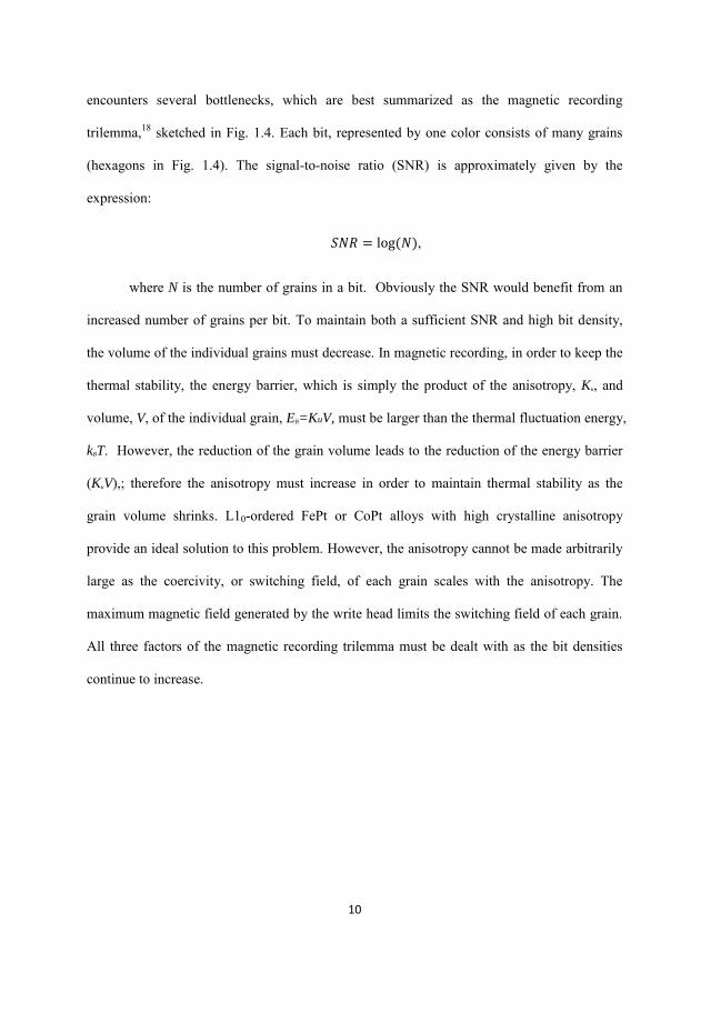
encounters several bottlenecks, which are best summarized as the magnetic recording
trilemma,18 sketched in Fig. 1.4. Each bit, represented by one color consists of many grains
(hexagons in Fig. 1.4). The signal-to-noise ratio (SNR) is approximately given by the
expression:
,
where N is the number of grains in a bit. Obviously the SNR would benefit from an
increased number of grains per bit. To maintain both a sufficient SNR and high bit density,
the volume of the individual grains must decrease. In magnetic recording, in order to keep the
thermal stability, the energy barrier, which is simply the product of the anisotropy, Ku, and
volume, V, of the individual grain, EB=KuV, must be larger than the thermal fluctuation energy,
kBT. However, the reduction of the grain volume leads to the reduction of the energy barrier
(KuV),; therefore the anisotropy must increase in order to maintain thermal stability as the
grain volume shrinks. L10-ordered FePt or CoPt alloys with high crystalline anisotropy
provide an ideal solution to this problem. However, the anisotropy cannot be made arbitrarily
large as the coercivity, or switching field, of each grain scales with the anisotropy. The
maximum magnetic field generated by the write head limits the switching field of each grain.
All three factors of the magnetic recording trilemma must be dealt with as the bit densities
continue to increase.
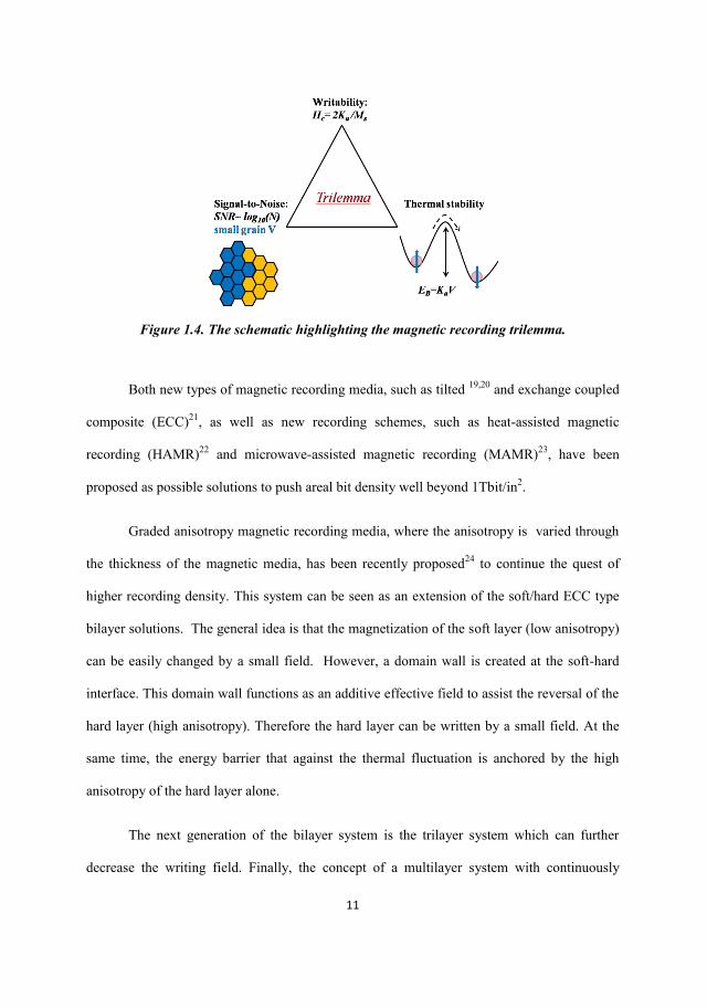
11
Figure 1.4. The schematic highlighting the magnetic recording trilemma.
Both new types of magnetic recording media, such as tilted 19,20 and exchange coupled
composite (ECC)21, as well as new recording schemes, such as heat-assisted magnetic
recording (HAMR)22 and microwave-assisted magnetic recording (MAMR)23, have been
proposed as possible solutions to push areal bit density well beyond 1Tbit/in2.
Graded anisotropy magnetic recording media, where the anisotropy is varied through
the thickness of the magnetic media, has been recently proposed24 to continue the quest of
higher recording density. This system can be seen as an extension of the soft/hard ECC type
bilayer solutions. The general idea is that the magnetization of the soft layer (low anisotropy)
can be easily changed by a small field. However, a domain wall is created at the soft-hard
interface. This domain wall functions as an additive effective field to assist the reversal of the
hard layer (high anisotropy). Therefore the hard layer can be written by a small field. At the
same time, the energy barrier that against the thermal fluctuation is anchored by the high
anisotropy of the hard layer alone.
The next generation of the bilayer system is the trilayer system which can further
decrease the writing field. Finally, the concept of a multilayer system with continuously

12
varying anisotropy is introduced and is referred as ‘‘graded media”.24 Fabrication of the so-
called ‘‘graded media” is challenging and has until now mostly based on the Co/Pd or Co/Pt
multilayer structure. In this thesis, we will discuss a simple approach to fabricate a
continuously graded-anisotropy single film and the resulting magnetic properties.
1.2.3 To remove the magnetic field requirement for spin torque oscillators:
spin polarizer with tilted anisotropy
Interest in the utilization of the STT effect,25,26 by which a spin polarized current can
switch or excite high frequency oscillations in a magnetic layer,27 is increasing due to a
wealth of potential device applications.28 In particular, research is mostly devoted to STT-
MRAM29 and spin-torque STO applications. The STOs are generally divided into two types
by geometry: nano-pillar30–32 and nano-contact STOs.33 In this thesis, we mainly focus on
nanocontact STOs.
The STO is a nano-scale spintronics device capable of microwave generation
frequencies in the 1- 60 GHz range with quality factors ( FWHMffQ / ) as high as 18,000.34
The microwave frequency can be tuned both by the drive current and an applied field.
Additional frequency tuning can also be achieved by varying the angle of the applied
magnetic field.35 They are relatively easy to fabricate in large quantities, and compatible with
standard silicon processing.
However, STOs typically have two major disadvantages for commercialization, first is
the low power output. This problem is able to be solved by increasing the GMR, or perhaps
even going to tunneling magnetoresistance (TMR), or synchronizing several STOs. Second is
STOs based on entirely in-plane anisotropy materials still require a large (in the order of a few
13
thousand Oersteds), static, external magnetic field for operation,36 which is one of the
challenges for future commercialization. Removing the need of the magnetic field is therefore
becoming an interesting topic for research. Several approaches have been proposed,
including the wavy-torque STOs,37 STOs with a perpendicular magnetic fixed layer,38 vortex
oscillations, 39–43 and tilted polarizer STOs.44–50
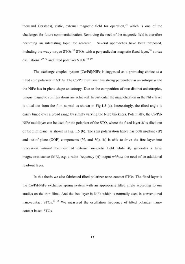
The exchange coupled system [Co/Pd]/NiFe is suggested as a promising choice as a
tilted spin polarizer in STOs. The Co/Pd multilayer has strong perpendicular anisotropy while
the NiFe has in-plane shape anisotropy. Due to the competition of two distinct anisotropies,
unique magnetic configurations are achieved. In particular the magnetization in the NiFe layer
is tilted out from the film normal as shown in Fig.1.5 (a). Interestingly, the tilted angle is
easily tuned over a broad range by simply varying the NiFe thickness. Potentially, the Co/Pd-
NiFe multilayer can be used for the polarizer of the STO, where the fixed layer M is tilted out
of the film plane, as shown in Fig. 1.5 (b). The spin polarization hence has both in-plane (IP)
and out-of-plane (OOP) components (Mx and Mz). Mz is able to drive the free layer into
precession without the need of external magnetic field while Mx generates a large
magnetoresistance (MR), e.g. a radio-frequency (rf) output without the need of an additional
read-out layer.
In this thesis we also fabricated tilted polarizer nano-contact STOs. The fixed layer is
the Co/Pd-NiFe exchange spring system with an appropriate tilted angle according to our
studies on the thin films. And the free layer is NiFe which is normally used in conventional
nano-contact STOs.51–53 We measured the oscillation frequency of tilted polarizer nano-
contact based STOs.
(a)
14
Figure 1.5 The schematics of tilted STO (a) and the schematic structure of the tilted polarizer composed with Co/Pd-NiFe exchange spring system with the magnetization tilted with respect to the film plane (b). is adjustable by varying the thickness of top NiFe
layer.

15
Chapter 2 Experimental methods
2.1 Fabrication techniques
2.1.1 Magnetron sputtering
Sputtering is one of the most widely used physical deposition techniques and is very
versatile with high yields. All vacuum compatible materials (with low enough vapor pressure)
can be sputtered, including metals, semiconductors, and insulators, either magnetic or non-
magnetic. Moreover, sputtering is able to grow high quality films with low roughness, rigid
adhesion to the substrate, and large-area thickness control. The main technique in this thesis
used to deposit thin films is called magnetron sputtering.
The main components of magnetron sputtering are schematically shown in Fig.2.1.
The sputtering guns are installed in the vacuum chamber which is simultaneously pumped by
the oil pump (which both provides a rough vacuum and “backs” the turbo pump) and turbo
pump to achieve the lowest possible base pressure. The source material (“target”) is mounted
in a Cu electrode which is water cooled and serves as a cathode. The target is eroded and
material ejected in the form of neutral particles travels to the surface of the substrate, e.g. Si
wafer. The substrate is transferred from a pre-pumped loadlock chamber and is able to rotate
during the deposition in order to deposit thin films with good uniformity. An electrically
isolated shield serves as the anode. The sputtering gun is attached to a power supply to
maintain the sputtering plasma state while the plasma is losing the energy into the
surroundings. The plasma state is a "dynamic condition" where neutral gas atoms, ions,
electrons, and photons exist in a near balanced state simultaneously. The magnets, hence
magnetron sputtering, in the cathode are helpful to confine the plasma near the target surface.
Typically an inert gas like Argon is utilized as the working gas. The working gas pressure in

16
the system is one of the basic parameters to be controlled during film deposition. For reactive
sputtering, oxygen and nitrogen gases can also be used, often simultaneously with Ar gas.
The following three steps highlighted by the dashed boxes in Fig.2.1 will give a more
comprehensive understanding of the sputtering process. Step 1: the ever present ‘‘free
electrons’’ are accelerated by an electric field, created between the negatively charged
electrode and the grounded gun shield anode. These accelerated electrons will bombard with
Ar atoms in their path, and will drive the outer shell electrons of the neutral gas atoms off,
resulting in an ionized Ar+ plasma. This step is hence called ionization (e-+Ar→ Ar++ 2e-).
Step 2: after ionization, the positively charged Ar ions (Ar+) are accelerated toward the
negatively charged electrode and strike the surface of the target. By simple energy transfer,
the Ar+ blasts loose a neutral particle from the target as well as more free electrons, which are
called secondary electrons. These additional electrons are useful for the ionization step and
preservation of the gaseous plasma. Step 3: the target atom reaches the substrate. The free
electrons, then find their way back into the outer shell of the Ar ion, thereby changing the ion
back into an electrically balanced Ar atom. Meanwhile, due to the conservation of energy, the
resultant gas atoms gain energy from the free electron and then release the energy in the form
of photons. Moreover, the secondary electrons may excite the Ar atoms into higher energy
levels which rapidly decay, emitting photons, and therefore the plasma appears to be glowing.
By using the magnets in the negatively charged electrode, the plasma is confined near the
surface of the target. This dramatically enhances the probability of ionizing a neutral gas and
the rate that the Ar ions bombard the target, allowing for a lower Ar working gas pressure.
However, it has the disadvantage of a more inhomogeneous target erosion than a simple
planar geometry. DC-magnetron sputtering (with a DC power supply attached to the target) is
usually limited to conducting materials like metals and doped semiconductors because the Ar+
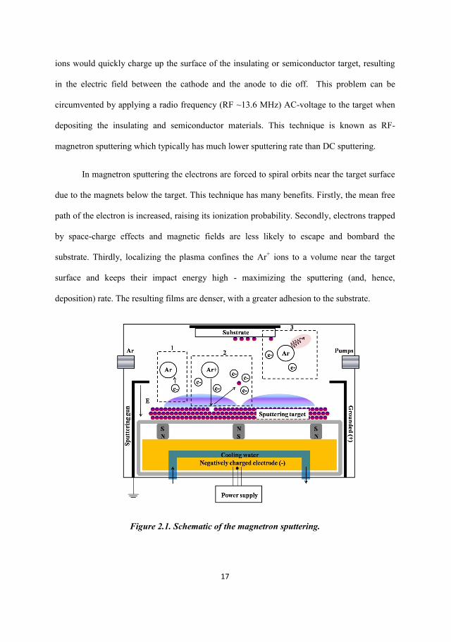
17
ions would quickly charge up the surface of the insulating or semiconductor target, resulting
in the electric field between the cathode and the anode to die off. This problem can be
circumvented by applying a radio frequency (RF ~13.6 MHz) AC-voltage to the target when
depositing the insulating and semiconductor materials. This technique is known as RF-
magnetron sputtering which typically has much lower sputtering rate than DC sputtering.
In magnetron sputtering the electrons are forced to spiral orbits near the target surface
due to the magnets below the target. This technique has many benefits. Firstly, the mean free
path of the electron is increased, raising its ionization probability. Secondly, electrons trapped
by space-charge effects and magnetic fields are less likely to escape and bombard the
substrate. Thirdly, localizing the plasma confines the Ar+ ions to a volume near the target
surface and keeps their impact energy high - maximizing the sputtering (and, hence,
deposition) rate. The resulting films are denser, with a greater adhesion to the substrate.
Figure 2.1. Schematic of the magnetron sputtering.
18
2.1.2 Fabrication of nano-contact STOs
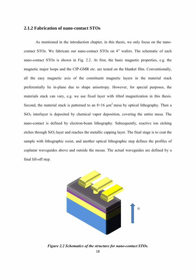
As mentioned in the introduction chapter, in this thesis, we only focus on the nano-
contact STOs. We fabricate our nano-contact STOs on 4” wafers. The schematic of each
nano-contact STOs is shown in Fig. 2.2. At first, the basic magnetic properties, e.g. the
magnetic major loops and the CIP-GMR etc. are tested on the blanket film. Conventionally,
all the easy magnetic axis of the constituent magnetic layers in the material stack
preferentially lie in-plane due to shape anisotropy. However, for special purposes, the
materials stack can vary, e.g. we use fixed layer with tilted magnetization in this thesis.
Second, the material stack is patterned to an 8×16 µm2 mesa by optical lithography. Then a
SiO2 interlayer is deposited by chemical vapor deposition, covering the entire mesa. The
nano-contact is defined by electron-beam lithography. Subsequently, reactive ion etching
etches through SiO2 layer and reaches the metallic capping layer. The final stage is to coat the
sample with lithographic resist, and another optical lithographic step defines the profiles of
coplanar waveguides above and outside the mesas. The actual waveguides are defined by a
final lift-off step.
Figure 2.2 Schematics of the structure for nano-contact STOs.

19
2.2 Structural characterization techniques
2.2.1 X-Ray Diffractometer
The high resolution Philips X’pert Material Research Diffractometer (MRD) is
utilized for structural characterization, e.g. crystalline structures and the interface roughnesses
of thin films in this thesis. The detailed discussions will be given later. The basic components
of this diffractometer are schematically shown in Fig. 2.3.
Figure 2.3 Schematics of the basic components for X-ray diffractormeter.
The high-speed electrons generated by a hot tungsten filament (cathode) are
accelerated by a high voltage toward the anode, which is a water-cooled block of Cu. A
variety of different materials (e.g. Cu, Al, Mo and Mg) can be used for the anode and each
generates X-rays with different characteristic wavelength. In our system, the Cu is used as the
desired target metal. The incident electrons release the orbital electrons of Cu from the K shell
(n=1). The electrons from the higher levels L (n=2) and M (n=3) may then drop down to fill
the void of the K shell, hence emitting the X-ray with specific wavelength. The characteristic
20
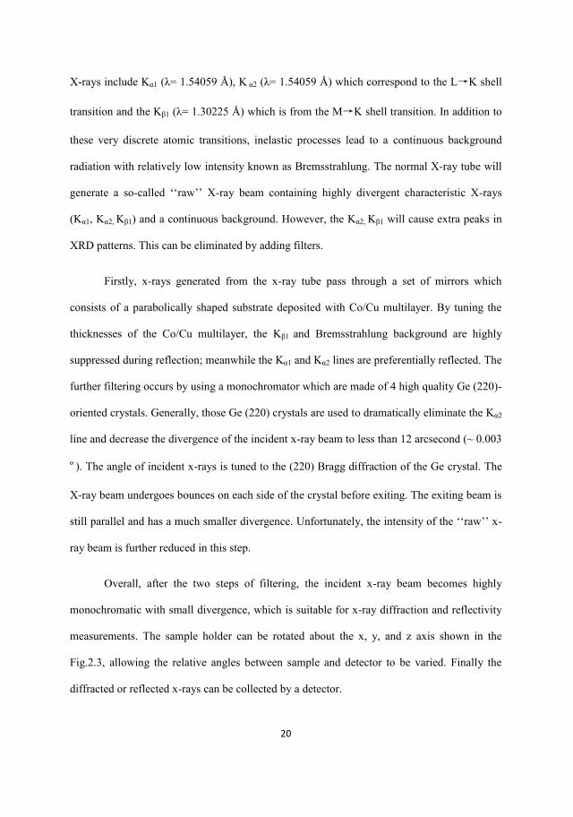
X-rays include Kα1 (λ= 1.54059 Å), K α2 (λ= 1.54059 Å) which correspond to the L→K shell
transition and the Kβ1 (λ= 1.30225 Å) which is from the M→K shell transition. In addition to
these very discrete atomic transitions, inelastic processes lead to a continuous background
radiation with relatively low intensity known as Bremsstrahlung. The normal X-ray tube will
generate a so-called ‘‘raw’’ X-ray beam containing highly divergent characteristic X-rays
(Kα1, Kα2, Kβ1) and a continuous background. However, the Kα2, Kβ1 will cause extra peaks in
XRD patterns. This can be eliminated by adding filters.
Firstly, x-rays generated from the x-ray tube pass through a set of mirrors which
consists of a parabolically shaped substrate deposited with Co/Cu multilayer. By tuning the
thicknesses of the Co/Cu multilayer, the Kβ1 and Bremsstrahlung background are highly
suppressed during reflection; meanwhile the Kα1 and Kα2 lines are preferentially reflected. The
further filtering occurs by using a monochromator which are made of 4 high quality Ge (220)-
oriented crystals. Generally, those Ge (220) crystals are used to dramatically eliminate the Kα2
line and decrease the divergence of the incident x-ray beam to less than 12 arcsecond (~ 0.003
º). The angle of incident x-rays is tuned to the (220) Bragg diffraction of the Ge crystal. The
X-ray beam undergoes bounces on each side of the crystal before exiting. The exiting beam is
still parallel and has a much smaller divergence. Unfortunately, the intensity of the ‘‘raw’’ x-
ray beam is further reduced in this step.
Overall, after the two steps of filtering, the incident x-ray beam becomes highly
monochromatic with small divergence, which is suitable for x-ray diffraction and reflectivity
measurements. The sample holder can be rotated about the x, y, and z axis shown in the
Fig.2.3, allowing the relative angles between sample and detector to be varied. Finally the
diffracted or reflected x-rays can be collected by a detector.
21
2.2.2 X-Ray Diffraction (XRD)
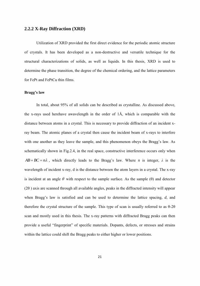
Utilization of XRD provided the first direct evidence for the periodic atomic structure
of crystals. It has been developed as a non-destructive and versatile technique for the
structural characterizations of solids, as well as liquids. In this thesis, XRD is used to
determine the phase transition, the degree of the chemical ordering, and the lattice parameters
for FePt and FePtCu thin films.
Bragg’s law
In total, about 95% of all solids can be described as crystalline. As discussed above,
the x-rays used herehave awavelength in the order of 1Å, which is comparable with the
distance between atoms in a crystal. This is necessary to provide diffraction of an incident x-
ray beam. The atomic planes of a crystal then cause the incident beam of x-rays to interfere
with one another as they leave the sample, and this phenomenon obeys the Bragg’s law. As
schematically shown in Fig.2.4, in the real space, constructive interference occurs only when
nBCAB , which directly leads to the Bragg’s law. Where n is integer, λ is the
wavelength of incident x-ray, d is the distance between the atom layers in a crystal. The x-ray
is incident at an angle with respect to the sample surface. As the sample (θ) and detector
(2θ ) axis are scanned through all available angles, peaks in the diffracted intensity will appear
when Bragg’s law is satisfied and can be used to determine the lattice spacing, d, and
therefore the crystal structure of the sample. This type of scan is usually referred to as θ-2θ
scan and mostly used in this thesis. The x-ray patterns with diffracted Bragg peaks can then
provide a useful “fingerprint” of specific materials. Dopants, defects, or stresses and strains
within the lattice could shift the Bragg peaks to either higher or lower positions.
22
Figure 2.4. Bragg’s law (left) and the scattering geometry (right).
In the reciprocal space, the condition for occurring constructive interference is: the
magnitude of the scattering vector, which is the vector between two reciprocal lattice points, l
Q l must equal nd
2 , Bragg’s law can also be derived in the same manner as in the real space,
as shown in Fig.2.4 :
QKK if, l
Q l =
sin4 , nd sin2
During the θ-2θ scan, the scattering vector is always perpendicular to the sample surface and
only a 1-dimensional line, along Qz, of reciprocal space is probed.
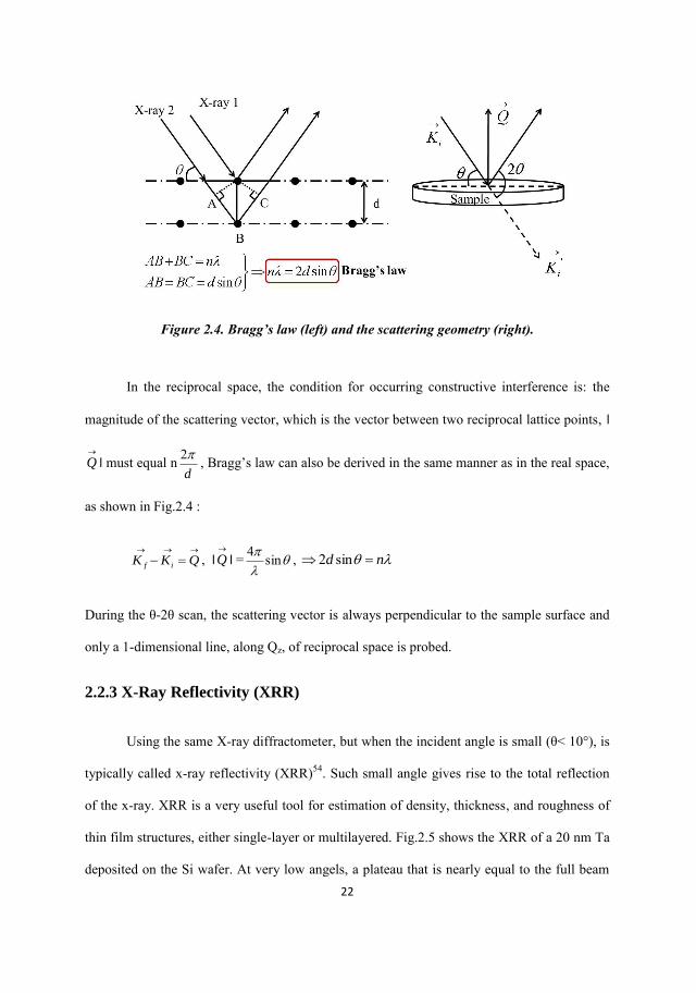
2.2.3 X-Ray Reflectivity (XRR)
Using the same X-ray diffractometer, but when the incident angle is small (θ< 10°), is
typically called x-ray reflectivity (XRR)54. Such small angle gives rise to the total reflection
of the x-ray. XRR is a very useful tool for estimation of density, thickness, and roughness of
thin film structures, either single-layer or multilayered. Fig.2.5 shows the XRR of a 20 nm Ta
deposited on the Si wafer. At very low angels, a plateau that is nearly equal to the full beam
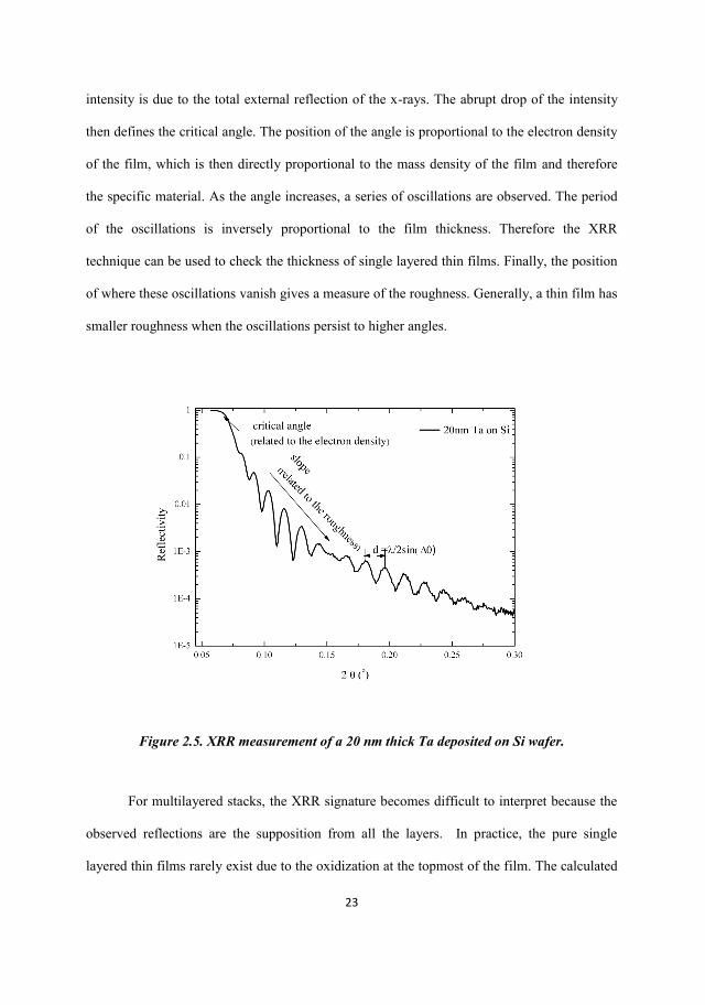
23
intensity is due to the total external reflection of the x-rays. The abrupt drop of the intensity
then defines the critical angle. The position of the angle is proportional to the electron density
of the film, which is then directly proportional to the mass density of the film and therefore
the specific material. As the angle increases, a series of oscillations are observed. The period
of the oscillations is inversely proportional to the film thickness. Therefore the XRR
technique can be used to check the thickness of single layered thin films. Finally, the position
of where these oscillations vanish gives a measure of the roughness. Generally, a thin film has
smaller roughness when the oscillations persist to higher angles.
Figure 2.5. XRR measurement of a 20 nm thick Ta deposited on Si wafer.
For multilayered stacks, the XRR signature becomes difficult to interpret because the
observed reflections are the supposition from all the layers. In practice, the pure single
layered thin films rarely exist due to the oxidization at the topmost of the film. The calculated
24
XRR data is then used to compare with the measured XRR data. The thickness, mass density,
and roughness of each layer are used as the fitting parameters until the calculated data and the
measured data almost overlap. The degree of overlapping gives a measure of the accuracy for
the parameters.
2.2.4 Atomic Force Microscopy (AFM)
An atomic force microscope is a type of scanning probe microscope used to
investigate the surface topology and mechanical properties using a sharp tip as the probe.
Unlike XRR which can probe the interface roughness of the multilayered stacks, AFM can
only detect the upmost layer, or surface, of a stack.
As in most scanning probe microscopes, an AFM consists of three primary parts: (i)
probe and scanning head, (ii) detection system (detector and electronics), and (iii) a control
unit with the feedback loop (Fig. 2. 6.). For the first part, the probe component is constructed
with a ~µm long and < 100 Å diameter sharp tip situated at the end of a cantilever, which is
generally more than several hundred µm long and coated with reflective material. The whole
piece is fabricated by the state-of-the-art technique and mounted on a piezo driven scanning
head which can provide both vertical and horizontal motion. Driven by this system, the tip can
be brought to within a very close distance to the substrate, where the atomic forces become
dominant. Consequently, the cantilever can be bent or deflected under the tip-substrate
interaction. By moving the tip relative to the substrate under the approached condition, the
cantilever can bend, following the surface topology. This small bending signal can be
measured by the detection system, which is usually a laser optical leverage unit including a
laser source and a split photodiode detector. By projecting the laser beam to the free end of
cantilever, the cantilever bending will be amplified by the beam reflection and the light signal

25
can be collected on the split photo-detector. Further conversion from optical signal to
electronic signal enables the control unit to interpret signal change referring to the set point
and translate either this signal change or feedback response into an image showing the
substrate geometric or mechanical characteristics.
Figure 2.6. Schematic of AFM components.
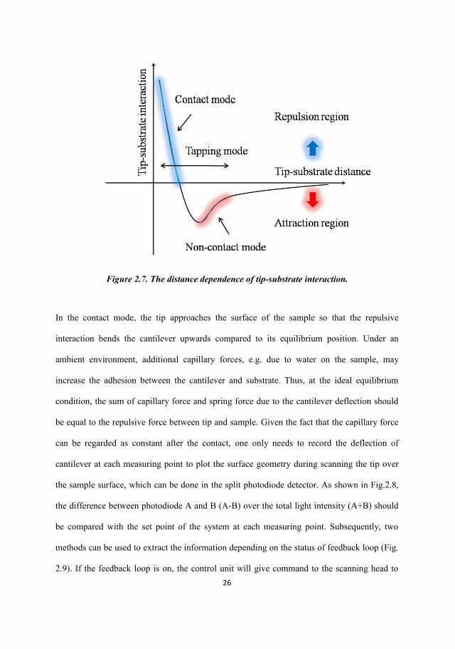
The tip-substrate interaction is a result of combined intermolecular interactions, with
the most common one being the van der Waal force. The distance dependence of tip-substrate
interaction is plotted in the Fig.2.7. Two working regimes, e.g. contact and non-contact, have
been marked in the repulsion and attraction interaction region, respectively. By approaching
tip in the appropriate regime, the AFM can work in the contact or non-contact mode.
Furthermore, AFM can image the substrate with a vibrating tip “tapping” the surface by
combining both virtue of contact mode and non-contact mode. In the following, we will give
more detailed description on each mode.
26
Figure 2.7. The distance dependence of tip-substrate interaction.
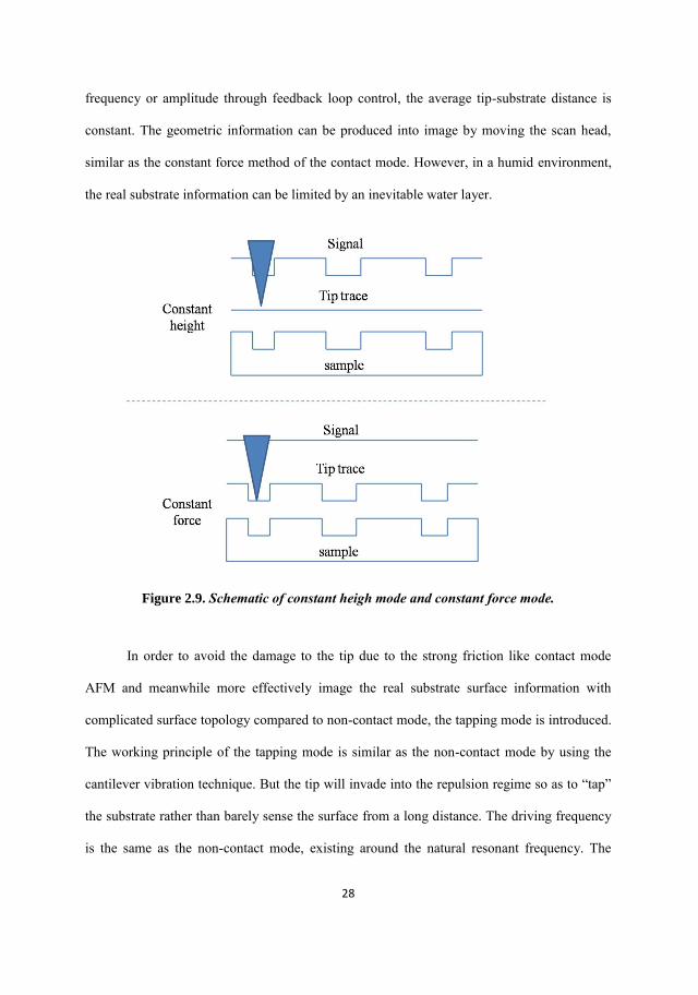
In the contact mode, the tip approaches the surface of the sample so that the repulsive
interaction bends the cantilever upwards compared to its equilibrium position. Under an
ambient environment, additional capillary forces, e.g. due to water on the sample, may
increase the adhesion between the cantilever and substrate. Thus, at the ideal equilibrium
condition, the sum of capillary force and spring force due to the cantilever deflection should
be equal to the repulsive force between tip and sample. Given the fact that the capillary force
can be regarded as constant after the contact, one only needs to record the deflection of
cantilever at each measuring point to plot the surface geometry during scanning the tip over
the sample surface, which can be done in the split photodiode detector. As shown in Fig.2.8,
the difference between photodiode A and B (A-B) over the total light intensity (A+B) should
be compared with the set point of the system at each measuring point. Subsequently, two
methods can be used to extract the information depending on the status of feedback loop (Fig.
2.9). If the feedback loop is on, the control unit will give command to the scanning head to
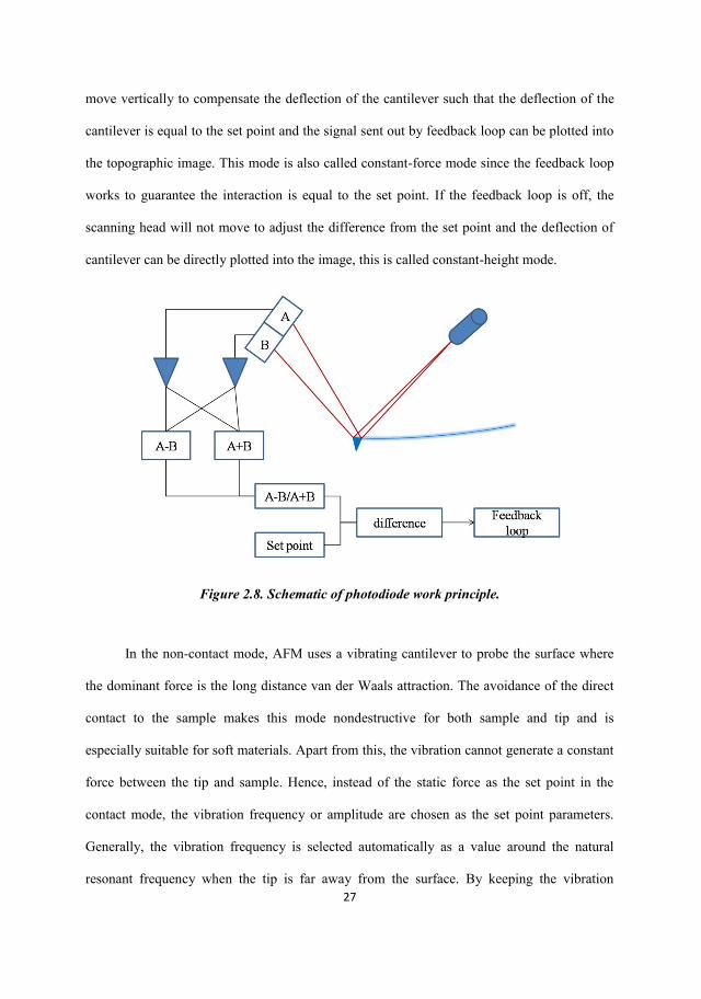
27
move vertically to compensate the deflection of the cantilever such that the deflection of the
cantilever is equal to the set point and the signal sent out by feedback loop can be plotted into
the topographic image. This mode is also called constant-force mode since the feedback loop
works to guarantee the interaction is equal to the set point. If the feedback loop is off, the
scanning head will not move to adjust the difference from the set point and the deflection of
cantilever can be directly plotted into the image, this is called constant-height mode.
Figure 2.8. Schematic of photodiode work principle.
In the non-contact mode, AFM uses a vibrating cantilever to probe the surface where
the dominant force is the long distance van der Waals attraction. The avoidance of the direct
contact to the sample makes this mode nondestructive for both sample and tip and is
especially suitable for soft materials. Apart from this, the vibration cannot generate a constant
force between the tip and sample. Hence, instead of the static force as the set point in the
contact mode, the vibration frequency or amplitude are chosen as the set point parameters.
Generally, the vibration frequency is selected automatically as a value around the natural
resonant frequency when the tip is far away from the surface. By keeping the vibration
28
frequency or amplitude through feedback loop control, the average tip-substrate distance is
constant. The geometric information can be produced into image by moving the scan head,
similar as the constant force method of the contact mode. However, in a humid environment,
the real substrate information can be limited by an inevitable water layer.
Figure 2.9. Schematic of constant heigh mode and constant force mode.
In order to avoid the damage to the tip due to the strong friction like contact mode
AFM and meanwhile more effectively image the real substrate surface information with
complicated surface topology compared to non-contact mode, the tapping mode is introduced.
The working principle of the tapping mode is similar as the non-contact mode by using the
cantilever vibration technique. But the tip will invade into the repulsion regime so as to “tap”
the substrate rather than barely sense the surface from a long distance. The driving frequency
is the same as the non-contact mode, existing around the natural resonant frequency. The
29
average tip-substrate distance is dependent on the amplitude variation and can be used as the
signal for the feedback control. By keeping the amplitude constant, the feedback response can
be plotted into the image as the contact mode (constant-force method). In this work, all the
measurements were done in this tapping mode given its advantages.
2.3 Magnetic properties characterization techniques
2.3.1 Magnetic Force Microscopy (MFM)
MFM is the main technique used in this thesis to investigate the magnetic domain structures of
thin films. MFM is sensitive to the magnetic stray field at the surface of the magnetic thin films. As
discussed in the AFM section, there are contact and non-contact modes in AFM. MFM imaging
utilizes the non-contact mode and magnetic tips. Prior to every measurement, the magnetic tip is
magnetized along the perpendicular direction by a small permanent magnet. During the measurement,
the tip is first scanned over the sample surface to obtain topographic information just as during an
AFM scan. Then the tip is raised just above the sample surface recorded by the first scan. The stray
fields influence the behavior of the tip. The lift height is an important parameter due to that the long-
range stay fields highly depend on the distance apart from the sample surface. When there is no
magnetic force, the cantilever has a resonance frequency f0, which is shifted by Δf proportional to
vertical gradients in the magnetic forces on the tip. The frequency shifts can be detected three ways:
phase detection, which measures the cantilever’s phase of oscillation relative to the piezo drive;
frequency modulation, which monitors the shifts of f0 ; and amplitude detection, which detects the
amplitude variance of the resonance frequency. Generally, phase detection and the frequency detection
give better results than amplitude detection. Phase detection is the main technique used in this thesis.
2.3.2 Vibrating Sample Magnetometer (VSM)
The basic measurement of the magnetic moment by VSM is accomplished by
oscillating the sample up and down near the pickup coil and simultaneously detecting the
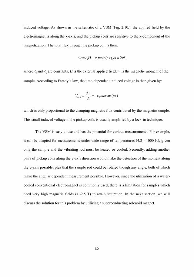
30
induced voltage. As shown in the schematic of a VSM (Fig. 2.10.), the applied field by the
electromagnet is along the x-axis, and the pickup coils are sensitive to the x-component of the
magnetization. The total flux through the pickup coil is then:
,2),sin(21 ftmcHc
where 1c and 2c are constants, H is the external applied field, m is the magnetic moment of the
sample. According to Farady’s law, the time-dependent induced voltage is then given by:
)cos(2 tmcdt
dVcoil
which is only proportional to the changing magnetic flux contributed by the magnetic sample.
This small induced voltage in the pickup coils is usually amplified by a lock-in technique.
The VSM is easy to use and has the potential for various measurements. For example,
it can be adapted for measurements under wide range of temperatures (4.2 - 1000 K), given
only the sample and the vibrating rod must be heated or cooled. Secondly, adding another
pairs of pickup coils along the y-axis direction would make the detection of the moment along
the y-axis possible, plus that the sample rod could be rotated though any angle, both of which
make the angular dependent measurement possible. However, since the utilization of a water-
cooled conventional electromagnet is commonly used, there is a limitation for samples which
need very high magnetic fields (>~2.5 T) to attain saturation. In the next section, we will
discuss the solution for this problem by utilizing a superconducting solenoid magnet.
31
Figure 2.10. A schematic of the conventional VSM with electromagnet.
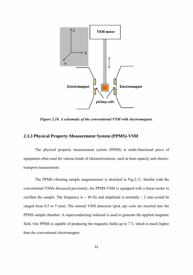
2.3.3 Physical Property Measurement System (PPMS)-VSM
The physical property measurement system (PPMS) is multi-functional piece of
equipment often used for various kinds of characterizations, such as heat capacity and electro-
transport measurement.
The PPMS-vibrating sample magnetometer is sketched in Fig.2.11. Similar with the
conventional VSMs discussed previously, the PPMS-VSM is equipped with a linear motor to
oscillate the sample. The frequency is ~ 40 Hz and amplitude is normally ~ 2 mm (could be
ranged from 0.5 to 5 mm). The normal VSM detection (pick up) coils are inserted into the
PPMS sample chamber. A superconducting solenoid is used to generate the applied magnetic
field. Our PPMS is capable of producing the magnetic fields up to 7 T, which is much higher
than the conventional electromagnet.

32
However, the superconducting magnet consumes a lot of liquid Helium (LHe).
Additionally, to perform the low temperature measurement, a vacuum pump draws LHe into
the annular region where heaters warm the gas to the correct temperature and a thermometer
is attached to monitor the temperature. These factors make the PPMS-VSM very expensive.
In this thesis, the PPMS-VSM-oven option is utilized to in-situ anneal and
magnetically characterize the sample. To perform the post annealing of the sample, a different
probe is designed. There are lines of Pt resistors on the front side of the sample holder to heat
up the sample. A thermocouple is attached at the backside of the PPMS-VSM-oven option
probe at the sample site to accurately monitor the temperature. The sample chamber is
evacuated to a pressure of 5×10⁻⁵ Torr in order to avoid the oxidization during the heating.
Figure 2.11. A schematic of PPMS sample chamber.
33
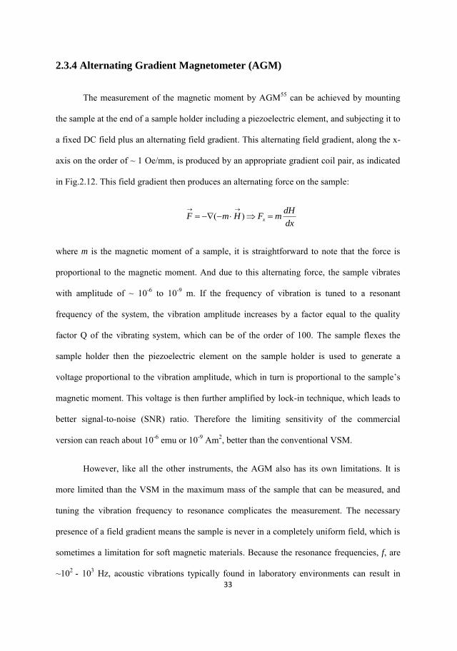
2.3.4 Alternating Gradient Magnetometer (AGM)
The measurement of the magnetic moment by AGM55 can be achieved by mounting
the sample at the end of a sample holder including a piezoelectric element, and subjecting it to
a fixed DC field plus an alternating field gradient. This alternating field gradient, along the x-
axis on the order of ~ 1 Oe/mm, is produced by an appropriate gradient coil pair, as indicated
in Fig.2.12. This field gradient then produces an alternating force on the sample:
dx
dHmFHmF x
)(
where m is the magnetic moment of a sample, it is straightforward to note that the force is
proportional to the magnetic moment. And due to this alternating force, the sample vibrates
with amplitude of ~ 10-6 to 10-9 m. If the frequency of vibration is tuned to a resonant
frequency of the system, the vibration amplitude increases by a factor equal to the quality
factor Q of the vibrating system, which can be of the order of 100. The sample flexes the
sample holder then the piezoelectric element on the sample holder is used to generate a
voltage proportional to the vibration amplitude, which in turn is proportional to the sample’s
magnetic moment. This voltage is then further amplified by lock-in technique, which leads to
better signal-to-noise (SNR) ratio. Therefore the limiting sensitivity of the commercial
version can reach about 10-6 emu or 10-9 Am2, better than the conventional VSM.
However, like all the other instruments, the AGM also has its own limitations. It is
more limited than the VSM in the maximum mass of the sample that can be measured, and
tuning the vibration frequency to resonance complicates the measurement. The necessary
presence of a field gradient means the sample is never in a completely uniform field, which is
sometimes a limitation for soft magnetic materials. Because the resonance frequencies, f, are
~102 - 103 Hz, acoustic vibrations typically found in laboratory environments can result in
34
significant noise in the measured data. In this thesis, the AGM is the primary tool for
measurement at room temperature, such as hysteresis loops and first order reversal curves.
Figure 2.12. A Schematic of an alternating gradient magnetometer.
2.3.5 Magneto-Optical Kerr Effect (MOKE)
As one of the variety interactions between the electromagnetic waves and
magnetically active material, the magneto-optical Kerr effect happens at the photon energies
near the visible part of the spectrum where interband transitions between conduction and
valence states take place.
Microscopically, the magneto-optic effects arise from the anti-symmetric, off-diagonal
elements in the dielectric tensor. These effects result in the polarization of the incident
radiation being rotated after transmission through (Faraday Effect) or reflection from (Kerr

35
Effect) a ferromagnetic material. In this thesis, the MOKE technique is employed to
investigate the depth dependent of the anisotropy for graded anisotropy material. The MOKE
will be discussed in great detail in the following section.
A microscopic description of MOKE relies on considering the different responses of
left and right circularly polarized light upon reflection. For a nonmagnetic material the
reflection coefficients for right and left circularly polarized light, rlcp and rrcp, are essentially
the same, while the magnetized sample has an effective magnetic field which gives provides
additional Lorentz force. Linearly polarized light generally becomes elliptically polarized
upon reflection, as shown in Fig.1.13. The major axis of the reflected light can be rotated of
an angle θK, known as the Kerr rotation, respect to the direction of the polarization of the
incident light, presenting an Kerr ellipticity K , )/arctan( baK , a and b are the lengths of
minor axis and major axis of the ellipse, respectively. The Kerr effect is then can be described
as the result of the polarization-specific reflectivity coefficients rlcp and rrcp.
Figure 2.13. Schematic of the magneto-optic Kerr effect.
36
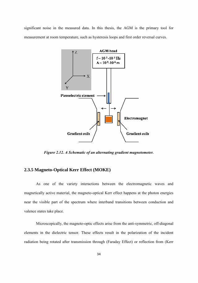
The MOKE56 measurements can be performed using three different geometric
configurations defined by the relative orientations of the sample magnetization
M , the
sample surface, and the plane of incidence of the light (Fig.2.14). When
M is perpendicular to
the sample surface, this geometry is known as polar MOKE. Longitudinal MOKE is the case
when
M is parallel to the sample surface and the plane of incidence. Finally the transverse
MOKE is the case when
M is parallel to the sample plane and perpendicular to the plane of
incidence.
Figure 2.14. The typical three configurations for MOKE measurement.
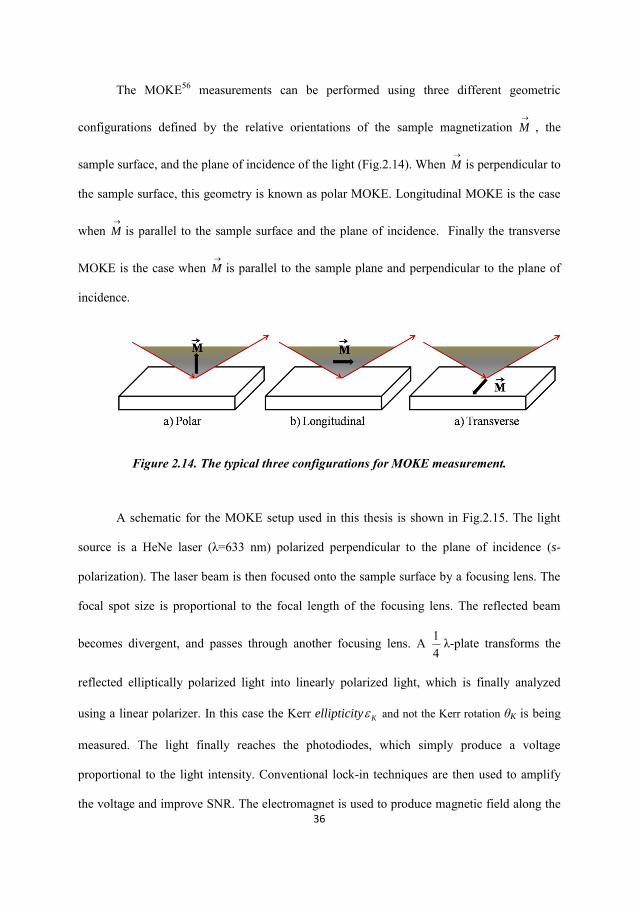
A schematic for the MOKE setup used in this thesis is shown in Fig.2.15. The light
source is a HeNe laser (λ=633 nm) polarized perpendicular to the plane of incidence (s-
polarization). The laser beam is then focused onto the sample surface by a focusing lens. The
focal spot size is proportional to the focal length of the focusing lens. The reflected beam
becomes divergent, and passes through another focusing lens. A 41 λ-plate transforms the
reflected elliptically polarized light into linearly polarized light, which is finally analyzed
using a linear polarizer. In this case the Kerr ellipticity K and not the Kerr rotation θK is being
measured. The light finally reaches the photodiodes, which simply produce a voltage
proportional to the light intensity. Conventional lock-in techniques are then used to amplify
the voltage and improve SNR. The electromagnet is used to produce magnetic field along the
37
x-axis and the intensity of field is measured by Hall probe. MOKE is surface sensitive
because the finite penetratration depth of the light. For most of the metals, the depth is about
~30nm.
Figure 2.15. Schematic of the MOKE magneometor.
2.3.6 First-Order Reversal Curve (FORC) technique
The magnetic reversal mechanism analysis in this thesis strongly depends on the
FORC technique. The roots of this technique can be traced back to ~75 years ago, when
Ferenc Preisach initially developed the Preisach model to describe any type of hysteretic
process, especially for ferromagnetic materials. After that, Mayergoyz57 first described this
method as a possible way to experimentally determine a Preisach distribution. The FORC
technique has recently evolved to be a very versatile tool for studying various properties (e.g.

38
magnetic, resistive, and ferroelectric). Most importantly, this technique is able to accurately
capture sufficient information of various ferromagnetic systems including bulk,58 thin
film,59,60 and patterned nanodisks,61,62 either at room temperatures or low temperatures
depending on the facilities.
The magnetometry techniques such as AGM, VSM, and MOKE which are discussed
before are used to measure a large number of FORCs in the following manner (Fig.2.16).
After positively saturating the sample, the applied field is then decreased to a given reversal
field, HR. The magnetization M is then measured from the reversal field back up to the
positive saturation, tracing out a FORC. A family of FORCs (~102 curves) is measured from
different HR, with equal field space, thereby filling the interior of the major hysteresis loop.
As described above, the measurement of FORCs is obviously time-consuming.
Figure 2.16. Family of FORCs for FePt(20nm)/CoFe(7nm) thin filmed measured by AGM with the magnetic field applied along the film plane.
39
FORC distributions
Just from simple analysis of the major loop (the boundary of family of FORCs) and
each FORC, a wealth of information about the magnetic reversal mechanism can be gained.
Whereas, the measured FORCs can yield larger amount of information by calculating the
FORC distribution, which is a mixed second order derivative of the normalized magnetization:
Where the factor 21
is included in the normalization of the magnetization and the negative
sign suggests that the FORCs are measured along the descending branch of the major loop. To
calculate ),( RHH , the consecutive data points of M (H, HR), a 2-dimentinal data array, are
locally fitted with a polynomial surface of the form :63
25
243210 RRR HaHaHHaHaHaa , then 32
1a is taken as the value of ),( RHH at
the center of the data array. The number of data points in each array is (2*SF+1)2, where SF
is refer to as ‘‘smoothing factor’’. The degree of smoothing increases with the value of the SF,
therefore normally we choose small value of SF for a well-behaved sample while a large
value is needed for a noisy sample. However, this numerical effect inevitably smoothes out
some of the potential features of the FORC distributions. In practice, it is not always trivial to
find the smallest value of SF as possible while keep the noisy at the acceptable level. The
FORC distributions are of little use if we are not able to correctly interpret them. When a
FORC distribution is plotted against H, HR, it is convenient to change the coordinates from
H, HR to HB= (H+HR)/2, HC = (H-HR)/2. The FORC distributions in different coordinates
systems have different interpretations. Fig.2.17 show FORC distributions of the
FePt(20nm)/CoFe(7nm) thin film plotted against (a) H, HR and (b) HB, HC coordinates.
,/),(21),(
2
R
SRR
HH
MHHMHH

40
Generally, in H, HR coordinate, the FORC distributions eliminate all the reversible
switching therefore capturing the irreversible switching. While the FORC distributions in HB,
HC coordinate is mainly used for comparing with the Preisach distribution.
Figure 2.17. FORC distributions of the FePt(20nm)/CoFe(7nm) thin film plotted in (a) H, HR coordinate and (b) HB, HC coordinate.
2.4 Transport measurements
2.4.1 DC characterization (Four probe measurement)
Current-in-plane (CIP)-GMR is measured by a home-made four probe measurement
setup with an applied magnetic field, as shown in Fig. 2.18. The four probes made of pogo
pins, the two outer probes provide the current and the two inner probes measure the voltage.
By rotating the motor, the magnetic field can be applied at any angle with respect to the film
plane. In contrast with current perpendicular-to-plane (CPP)-GMR which normally requires
lithography for nano-pillar fabrication, CIP-GMR can be measured directly on the deposited
blanket thin film. The electrical resistance of spinvalve stack depends on the relative direction
41
of the free and fixed layer. When the free layer and fixed layer are antiparallel, the resistance
RAP is relatively high. The resistance RP is relatively low when the free and fixed layers are
parallel. The GMR ratio is then defined as (RAP-RP)/RP. A high GMR ratio is normally
required for magnetic memories, sensors, and to maximize the spin-transfer toque effect.
Figure 2.18 Schematics of the four probe measurement.
2.4.2 High frequency measurement setup
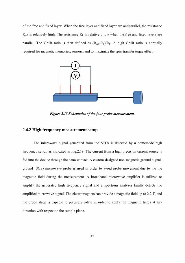
The microwave signal generated from the STOs is detected by a homemade high
frequency set-up as indicated in Fig.2.19. The current from a high precision current source is
fed into the device through the nano-contact. A custom-designed non-magnetic ground-signal-
ground (SGS) microwave probe is used in order to avoid probe movement due to the the
magnetic field during the measurement. A broadband microwave amplifier is utilized to
amplify the generated high frequency signal and a spectrum analyzer finally detects the
amplified microwave signal. The electromagnets can provide a magnetic field up to 2.2 T, and
the probe stage is capable to precisely rotate in order to apply the magnetic fields at any
direction with respect to the sample plane.
42
Figure 2.19. Schematics of the setup for detecting the microwave signal generated by the STOs.

43
Chapter 3 Results and discussions
3.1 Non-volatile spintronics element with continuous different
resistance levels (Paper I)
As discussed in the introduction, increasing the magnetic storage capacity is
perpetually in demand. The conventional digital magnetic storage devices depend on the
realization of two stable magnetic states in each bit to encode information.64 Intensive
research has been devoted to the approaches aiming for reducing the individual memory cell
size to increase the memory density. An alternative scheme is to increase the number of states
allowed in each memory cell.
We have fabricated our thin film samples by magnetron sputtering. Our device has a
typical PSV structure as schematically shown in Fig.3.1. Both the free layer and the fixed
layer are Co/Pd multilayers with perpendicular anisotropy that is with the easy axis
perpendicular to the film plane. The fixed layer is [Co (0.25)/Pd(0.6)]10 Co(0.25) multilayer
with the Co thickness fixed (thicknesses are in nm). The Co thickness in free layer is
incremented by 0.1 nm for successive repeats of the Co/Pd unit, therefore leading to the
gradually varying perpendicular anisotropy14 in each unit through the whole free layer.
Figure 3.1. Schematic of the pseudo spinvalve showing the graded anisotropy free layer on top separated from the fixed layer on bottom by a Cu spacer (all the thickness is nm).
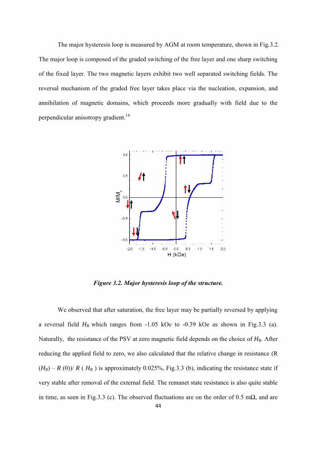
44
The major hysteresis loop is measured by AGM at room temperature, shown in Fig.3.2.
The major loop is composed of the graded switching of the free layer and one sharp switching
of the fixed layer. The two magnetic layers exhibit two well separated switching fields. The
reversal mechanism of the graded free layer takes place via the nucleation, expansion, and
annihilation of magnetic domains, which proceeds more gradually with field due to the
perpendicular anisotropy gradient.14
Figure 3.2. Major hysteresis loop of the structure.
We observed that after saturation, the free layer may be partially reversed by applying
a reversal field HR which ranges from -1.05 kOe to -0.39 kOe as shown in Fig.3.3 (a).
Naturally, the resistance of the PSV at zero magnetic field depends on the choice of HR. After
reducing the applied field to zero, we also calculated that the relative change in resistance (R
(HR) – R (0))/ R ( HR ) is approximately 0.025%, Fig.3.3 (b), indicating the resistance state if
very stable after removal of the external field. The remanet state resistance is also quite stable
in time, as seen in Fig.3.3 (c). The observed fluctuations are on the order of 0.5 mΩ, and are
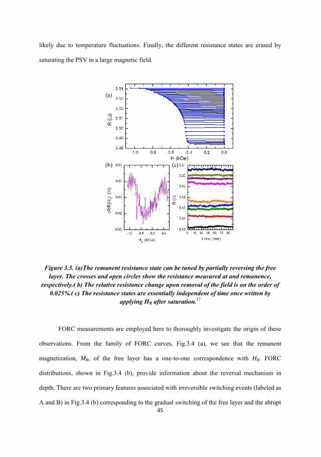
45
likely due to temperature fluctuations. Finally, the different resistance states are erased by
saturating the PSV in a large magnetic field.
Figure 3.3. (a)The remanent resistance state can be tuned by partially reversing the free layer. The crosses and open circles show the resistance measured at and remanence,
respectively.( b) The relative resistance change upon removal of the field is on the order of 0.025%.( c) The resistance states are essentially independent of time once written by
applying HR after saturation.17
FORC measurements are employed here to thoroughly investigate the origin of these
observations. From the family of FORC curves, Fig.3.4 (a), we see that the remanent
magnetization, MR, of the free layer has a one-to-one correspondence with HR. FORC
distributions, shown in Fig.3.4 (b), provide information about the reversal mechanism in
depth. There are two primary features associated with irreversible switching events (labeled as
A and B) in Fig.3.4 (b) corresponding to the gradual switching of the free layer and the abrupt

46
switching of the fixed layer, respectively. The horizontal ridge noted by Line 1 in Fig.3.4 (b)
corresponds to the precipitous and irreversible drop in magnetization of graded free layer
when reverse domains are nucleated. The vertical negative/positive pair of peaks noted by
Line 2 in Fig.3.4 (b) indicates irreversible domain annihilation as negative saturation is
approached. The region between Lines 1 and 2 has no peaks but has non-zero FORC
distributions,implying a gradual and irreversible magnetization reversal process. The FORC
distribution is featureless between areas A and B, consistent with the well-defined antiparallel
state seen in both the major magnetic hysteresis loop and MR data.
Figure 3.4 (a) Family of FORCs for the PSV, with the first point of the individual reversal curves shown by a black dot. (b) The FORC distribution reveals features related to the
reversal of the free layer (area A) and fixed layer (area B).17
MFM directly reveals the tunability of the domain configurations in the free layer as a
function of the reversal field. We measured the MFM images at zero field after applying HR ,
as shown in Fig.3.5. As the magnitude of HR increases, the total area of the down (bright)
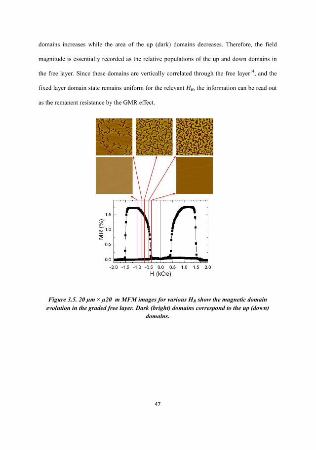
47
domains increases while the area of the up (dark) domains decreases. Therefore, the field
magnitude is essentially recorded as the relative populations of the up and down domains in
the free layer. Since these domains are vertically correlated through the free layer14, and the
fixed layer domain state remains uniform for the relevant HR, the information can be read out
as the remanent resistance by the GMR effect.
Figure 3.5. 20 µm × µ20 m MFM images for various HR show the magnetic domain evolution in the graded free layer. Dark (bright) domains correspond to the up (down)
domains.
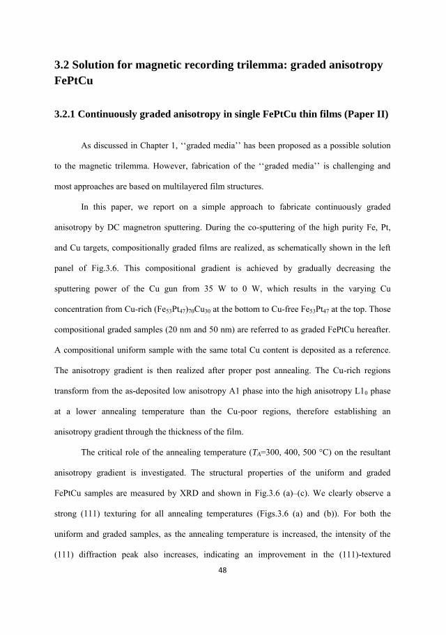
48
3.2 Solution for magnetic recording trilemma: graded anisotropy
FePtCu
3.2.1 Continuously graded anisotropy in single FePtCu thin films (Paper II)
As discussed in Chapter 1, ‘‘graded media’’ has been proposed as a possible solution
to the magnetic trilemma. However, fabrication of the ‘‘graded media’’ is challenging and
most approaches are based on multilayered film structures.
In this paper, we report on a simple approach to fabricate continuously graded
anisotropy by DC magnetron sputtering. During the co-sputtering of the high purity Fe, Pt,
and Cu targets, compositionally graded films are realized, as schematically shown in the left
panel of Fig.3.6. This compositional gradient is achieved by gradually decreasing the
sputtering power of the Cu gun from 35 W to 0 W, which results in the varying Cu
concentration from Cu-rich (Fe53Pt47)70Cu30 at the bottom to Cu-free Fe53Pt47 at the top. Those
compositional graded samples (20 nm and 50 nm) are referred to as graded FePtCu hereafter.
A compositional uniform sample with the same total Cu content is deposited as a reference.
The anisotropy gradient is then realized after proper post annealing. The Cu-rich regions
transform from the as-deposited low anisotropy A1 phase into the high anisotropy L10 phase
at a lower annealing temperature than the Cu-poor regions, therefore establishing an
anisotropy gradient through the thickness of the film.
The critical role of the annealing temperature (TA=300, 400, 500 °C) on the resultant
anisotropy gradient is investigated. The structural properties of the uniform and graded
FePtCu samples are measured by XRD and shown in Fig.3.6 (a)–(c). We clearly observe a
strong (111) texturing for all annealing temperatures (Figs.3.6 (a) and (b)). For both the
uniform and graded samples, as the annealing temperature is increased, the intensity of the
(111) diffraction peak also increases, indicating an improvement in the (111)-textured
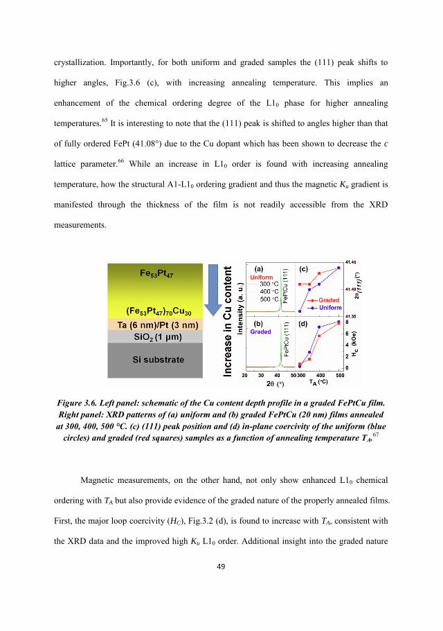
49
crystallization. Importantly, for both uniform and graded samples the (111) peak shifts to
higher angles, Fig.3.6 (c), with increasing annealing temperature. This implies an
enhancement of the chemical ordering degree of the L10 phase for higher annealing
temperatures.65 It is interesting to note that the (111) peak is shifted to angles higher than that
of fully ordered FePt (41.08°) due to the Cu dopant which has been shown to decrease the c
lattice parameter.66 While an increase in L10 order is found with increasing annealing
temperature, how the structural A1-L10 ordering gradient and thus the magnetic Ku gradient is
manifested through the thickness of the film is not readily accessible from the XRD
measurements.
Figure 3.6. Left panel: schematic of the Cu content depth profile in a graded FePtCu film. Right panel: XRD patterns of (a) uniform and (b) graded FePtCu (20 nm) films annealed
at 300, 400, 500 °C. (c) (111) peak position and (d) in-plane coercivity of the uniform (blue circles) and graded (red squares) samples as a function of annealing temperature TA.67
Magnetic measurements, on the other hand, not only show enhanced L10 chemical
ordering with TA but also provide evidence of the graded nature of the properly annealed films.
First, the major loop coercivity (HC), Fig.3.2 (d), is found to increase with TA, consistent with
the XRD data and the improved high Ku L10 order. Additional insight into the graded nature
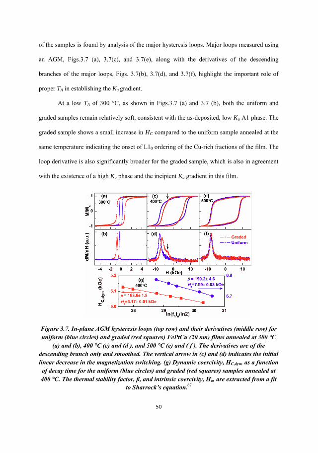
50
of the samples is found by analysis of the major hysteresis loops. Major loops measured using
an AGM, Figs.3.7 (a), 3.7(c), and 3.7(e), along with the derivatives of the descending
branches of the major loops, Figs. 3.7(b), 3.7(d), and 3.7(f), highlight the important role of
proper TA in establishing the Ku gradient.
At a low TA of 300 °C, as shown in Figs.3.7 (a) and 3.7 (b), both the uniform and
graded samples remain relatively soft, consistent with the as-deposited, low Ku A1 phase. The
graded sample shows a small increase in HC compared to the uniform sample annealed at the
same temperature indicating the onset of L10 ordering of the Cu-rich fractions of the film. The
loop derivative is also significantly broader for the graded sample, which is also in agreement
with the existence of a high Ku phase and the incipient Ku gradient in this film.
Figure 3.7. In-plane AGM hysteresis loops (top row) and their derivatives (middle row) for uniform (blue circles) and graded (red squares) FePtCu (20 nm) films annealed at 300 °C
(a) and (b), 400 °C (c) and (d ), and 500 °C (e) and ( f ). The derivatives are of the descending branch only and smoothed. The vertical arrow in (c) and (d) indicates the initial linear decrease in the magnetization switching. (g) Dynamic coercivity, HC,dyn, as a function of decay time for the uniform (blue circles) and graded (red squares) samples annealed at 400 °C. The thermal stability factor, β, and intrinsic coercivity, Ho, are extracted from a fit
to Sharrock’s equation.67

51
At an intermediate TA of 400 °C, Figs.3.7 (c) and 2 (d), the HC of both the graded and
uniform films dramatically increases as a larger fraction of the films transforms into the high
Ku L10 phase. Interestingly, after annealing at 400 °C, the graded film exhibits a
fundamentally different reversal path compared to the uniform film. As we can clearly see
from the derivatives, Fig.3.7 (d), the graded sample exhibits an asymmetric peak with an
extended switching shoulder. This shoulder corresponds to the softer portions of the film
beginning to reverse first. In fact, the overall shape of the loop is reminiscent of simulated
hysteresis curves of films with a graded Ku that show an initial linear decrease in the
magnetization (see arrow in Fig.3.7 (c)).68 The initial linear decay of the magnetization can be
associated with the formation of a partial domain wall through the film thickness that
precedes switching. Actually the plateau in the major loop derivative (see arrow in Fig.3.2 (d))
directly indicates this initial linear decrease in the magnetization. Most importantly, the
coercivity of the compositionally graded film, HC=5.67 kOe, is smaller than the uniform film,
HC=7.21 kOe, which is also consistent with the existence of a Ku gradient. Additionally, the
remanence (Mr/Ms where Mr and Ms are the remnant and saturation magnetizations,
respectively), of the graded sample, Mr/Ms =0.91, is larger than the uniform sample, Mr/Ms
=0.79. This implies that the graded sample has a substantial fraction of soft phase.
To assess the thermal stability of our graded samples we have carried out dynamic HC
measurements. The dynamic HC, HC,dyn, is the field required to bring the magnetization to zero
after a characteristic time, to, and functionally obeys Sharrock’s equation.69 In our calculations,
an attempt frequency fo=5×10⁹ Hz is used and we can presume n=1.68 From this analysis, the
thermal stability factor (E0/kBT) and time independent intrinsic HC, Ho, can then be extracted.
Here Eo is the energy barrier and kBT is the thermal activation energy. The HC,dyn
measurements for the uniform and graded films annealed at 400 °C are shown in Fig.3.7(g)

52
where we find Ho=7.99±0.03 kOe, β=190.2±4.6 and Ho=6.17±0.01 kOe, β =163.6±1.8, for the
uniform and graded samples, respectively. Although the graded sample shows a small, 14%,
decrease in thermal stability, it also shows a significantly larger, 23%, decrease in Ho.
The AGM, which measures the total magnetic moment, is not able to directly
determine how the Ku varies through the thickness of the film. To probe the graded Ku we
have measured surface magnetic properties of a 50 nm thick graded FePtCu film using the
MOKE where the finite penetration depth of light (~30 nm in FePt) can be exploited. The
MOKE and AGM in-plane loops are shown in Fig.3.8 (a) for a sample annealed at 300 °C.
Clearly the MOKE loop has a smaller coercivity, HC, MOKE=1.31 kOe, than the AGM loop, HC,
AGM=1.92 kOe and exhibits a different reversal path. As expected, the MOKE loop, which
only probes the upper portions of the film, is significantly softer because the Cu-poor regions
near the top of the film have not fully transformed into the high Ku L10 phase at this particular
TA. These depth sensitive results, along with the observed in-plane easy axis (induced by the
thin film shape anisotropy), confirm that the anisotropy varies through the film thickness
instead of forming, e.g., random L10 clusters embedded in an A1 matrix. However, after
annealing at 400 °C both the AGM and MOKE loops, Fig.3.8 (b), have the same HC, HC,
AGM=HC,MOKE=7.03 kOe, and nearly identical loop shape. This indicates that after annealing at
400 °C the 50 nm graded FePtCu film has achieved a uniform Ku distribution, similar to the
20 nm thick samples annealed at 500 °C. As reported for uniform FePtCu films, the L10
chemical ordering process also depends on film thickness and is actually promoted in thicker
films. 70
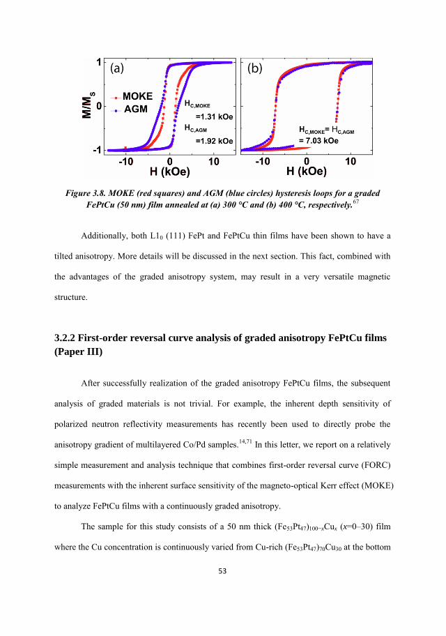
53
Figure 3.8. MOKE (red squares) and AGM (blue circles) hysteresis loops for a graded FePtCu (50 nm) film annealed at (a) 300 °C and (b) 400 °C, respectively.67
Additionally, both L10 (111) FePt and FePtCu thin films have been shown to have a
tilted anisotropy. More details will be discussed in the next section. This fact, combined with
the advantages of the graded anisotropy system, may result in a very versatile magnetic
structure.
3.2.2 First-order reversal curve analysis of graded anisotropy FePtCu films
(Paper III)
After successfully realization of the graded anisotropy FePtCu films, the subsequent
analysis of graded materials is not trivial. For example, the inherent depth sensitivity of
polarized neutron reflectivity measurements has recently been used to directly probe the
anisotropy gradient of multilayered Co/Pd samples.14,71 In this letter, we report on a relatively
simple measurement and analysis technique that combines first-order reversal curve (FORC)
measurements with the inherent surface sensitivity of the magneto-optical Kerr effect (MOKE)
to analyze FePtCu films with a continuously graded anisotropy.
The sample for this study consists of a 50 nm thick (Fe53Pt47)100−xCux (x=0–30) film
where the Cu concentration is continuously varied from Cu-rich (Fe53Pt47)70Cu30 at the bottom
54
to Cu-free Fe53Pt47 at the top. The Cu-rich regions transform from the as-deposited low
anisotropy cubic A1 phase into the high anisotropy tetragonal L10 phase at a lower annealing
temperature than the Cu-poor regions, thus establishing a continuous anisotropy gradient
through the thickness of the film. Separate pieces of the as-deposited film were then annealed
at 300 and 400 °C for 35 min in vacuum. The detailed information about sample fabrication
and structural analysis can be found in paper II, similar with the 20 nm thick films.
Magnetic properties have been measured using an AGM and MOKE in the
longitudinal configuration using a diode laser (λ=633 nm) polarized perpendicular to the
plane of incidence (s-polarization). The AGM measures the magnetic response of the entire
film and gives an overall view of the magnetization reversal, whereas the MOKE
measurements preferentially sample the surface of the film. We have estimated the
penetration depth of light (~30 nm), employing the optical properties of bulk FePt.72 All the
measurements are performed at room temperature with the field applied parallel to the film
plane and along the same in-plane direction, given any potential in-plane anisotropy. In
chapter 2, we have discussed the FORC technique and the FORC distribution which is defined
as:
Often it is better to have a one-dimensional visualization of the irreversibility (see
chapter 2) by projecting the FORC distribution onto the HR-axis in H, HR coordinates. This
is equivalent to an integration over the applied field H:
R
R
R
R
H
HMdH
HH
HHM
)(),(2
This is termed a FORC-switching field distribution (FORC-SFD), which can then be
easily compared with the standard technique of taking the derivative of the dc-
,/),(21),(
2
R
SRR
HH
MHHMHH
55
demagnetization curve to determine the dc-demagnetization switching field distribution
(DCD-SFD): R
Rr
H
HM
)( , where )( Rr HM is the zero-field magnetization, or remanence, after
the application of a given reversal field HR.
The family of FORCs and corresponding FORC distributions measured by AGM and
MOKE are shown in Figs.3.9 (a) and 3.9 (c) and Figs. 3.9 (b) and 3.9(d), respectively. For the
graded FePtCu film annealed at 300 °C, the AGM major loop, seen as the outer boundary of
the FORCs, shows a rather gradual reversal process and a coercivity of 1.98 kOe Fig. 3.9 (a).
A close inspection reveals that the major loop appears slightly pinched, which suggests the
presence of both soft and hard phases. The AGM-DCD-SFD shows a large peak located at
HR=−3.5 kOe (Fig. 3.9(a)) (solid squares), which indicates that the majority of the switching
processes occur for this reversal field. However, upon closer inspection a second and much
smaller peak located at HR=−1.7 kOe (indicated with an arrow) indicates the presence of soft
phase switching. Interestingly, the soft phase only becomes fully evident in the full FORC
analysis. The AGM-FORC distribution (Fig. 3.9 (b)) shows two primary features. The first
feature, highlighted with a dashed circle, is a sharp and localized peak located near the H=HR
boundary and can be associated with a soft phase as it occurs for small HR values. The second
feature, highlighted with a solid oval, is a negative-positive pair of features that extend
downward parallel to the HR-axis and can be associated with the hard phase. From a
fingerprinting standpoint, this FORC distribution is reminiscent of those previously observed
in soft/hard bilayer exchange springs.60 In order to better compare with the AGM-DCD-SFD,
the AGM-FORC-SFD is calculated (Fig.3.9 (a) (solid circles)) and shows two distinct peaks.
Unlike the AGM-DCD-SFD, the soft phase peak, located at HR=−1.7 kOe, is not only
enhanced but also slightly larger than the hard phase peak located at HR=−3.5 kOe. The
significant overlap between the soft and hard peaks indicates that these phases are indeed

56
highly coupled. An inspection of the minor loop bounded by the descending branch of the
major loop and the highlighted FORC in Fig.3.9 (a) HR=−1.7 kOe reveals a clear shift toward
negative fields due to a significant exchange coupling to the hard phase. In fact, the striking
differences between the AGM-DCD-SFD and AGM-FORC-SFD is in stark contrast to what
has been previously observed in standard bilayer exchange spring systems where only minor
differences were evident.60 The difference between the AGM-DCD-SFD and the AGM-
FORC-SFD arises because the AGM-DCD-SFD is only sensitive to switching events as they
are manifested at the remanent state, whereas the AGM-FORC-SFD accounts for
irreversibility along the entire reversal curve. During the soft phase reversal, the remanent
state changes very little because the soft phase minor loop is significantly exchange shifted
toward the left, which renders it virtually invisible in the AGM-DCD-SFD. However, the
FORC analysis, which is sensitive to the total irreversibility present, is able to clearly resolve
the soft and hard layers alike. It must be noted that while the AGM-FORC analysis is able to
reveal the soft/hard components, it is not able to directly probe how they are distributed
through the film thickness.

57
Figure 3.9. Families of FORCs for the graded FePtCu film annealed at 300 °C measured using the (a) AGM and (c) MOKE, where the first point of each FORC is shown by a dot. The corresponding FORC distributions are shown in (b) and (d), respectively. The bold FORC in (a) indicates the initial soft phase portion of the reversal and the dashed circle
and solid oval highlight the soft and hard portions of the reversal, respectively.73
In order to selectively probe the surface of the film, MOKE measurements are
performed. The family of FORC curves measured using the MOKE is shown in Fig.3.9 (c).
Clearly, the major loop exhibits a different reversal behavior as that observed using the AGM.
The reversal begins with a sharp decrease in magnetization followed by a more gradual
approach toward saturation. Most notably, the MOKE major loop shows a reduced coercivity
of 1.28 kOe as compared to the AGM measurements, which indicates that the softer portions
of the sample are indeed near the surface, as designed. The MOKE-DCD-SFD is shown in Fig.
3.10 (b) (open squares). While both the AGM and MOKE-DCD-SFDs reveal two peaks, two
distinct differences are observed. First, the high anisotropy peak is shifted toward less
negative reversal fields(HR=−2.7 kOe). Second, the high and low anisotropy peaks now have
comparable amplitudes. Both of these differences are consistent with the fact that the MOKE
measurements preferentially probe the lower anisotropy layers near the surface. A comparison
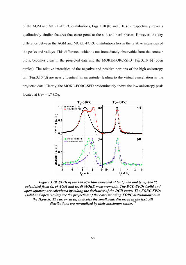
58
of the AGM and MOKE-FORC distributions, Figs.3.10 (b) and 3.10 (d), respectively, reveals
qualitatively similar features that correspond to the soft and hard phases. However, the key
difference between the AGM and MOKE-FORC distributions lies in the relative intensities of
the peaks and valleys. This difference, which is not immediately observable from the contour
plots, becomes clear in the projected data and the MOKE-FORC-SFD (Fig. 3.10 (b) (open
circles). The relative intensities of the negative and positive portions of the high anisotropy
tail (Fig.3.10 (d) are nearly identical in magnitude, leading to the virtual cancellation in the
projected data. Clearly, the MOKE-FORC-SFD predominately shows the low anisotropy peak
located at HR= −1.7 kOe.
Figure 3.10. SFDs of the FePtCu film annealed at (a, b) 300 and (c, d) 400 °C calculated from (a, c) AGM and (b, d) MOKE measurements. The DCD-SFDs (solid and open squares) are calculated by taking the derivative of the DCD curve. The FORC-SFDs (solid and open circles) are the projection of the corresponding FORC distributions onto
the HR-axis. The arrow in (a) indicates the small peak discussed in the text. All distributions are normalized by their maximum values.73
59
3.2.3 An in-situ anneal study of graded anisotropy FePtCu films (Paper IV)
As discussed in paper II and III, we found that the post-annealing temperature (TA)
plays an important role on the induced anisotropy gradient. In this paper, we carry out a
detailed study of how the anisotropy gradient gradually develops in a 20 nm thick
compositionally graded FePtCu thin film as a function of the TA. A detailed stepwise analysis
is achieved by exploiting the in situ anneal and magnetic characterization capabilities of a
physical property measurement system (PPMS) equipped with a vibrating sample
magnetometer (VSM) that allows us to follow the development of the coercivity, the reversal
mechanisms, the saturation magnetization, and the overall hysteresis loop shape with
unprecedented accuracy and control. By only mounting the sample once, the approach is
entirely immune to external sources of measurement error from remounting and recalibration,
and hence, all magnetic characterization can be directly compared. The sample we use in this
paper is the 20 thick graded FePtCu films. The details of this sample fabrication have been
discussed in paper II.
A representative selection of hysteresis loops (left) and the corresponding derivatives
of their descending branches (right) for a number of anneal temperatures are shown in Fig.
3.11. At the lowest TA (300 °C), the major loop exhibits a single sharp switching event and a
relatively low HC. Additionally, the derivative of the major loop is far narrower than those
observed for higher TA. Both observations suggest that the film primarily consists of a single
uniform low-Ku A1 phase. At intermediate TA (320 – 475 °C), on the other hand, the
hysteresis loops and the corresponding derivatives become significantly more complex,
indicating an evolving anisotropy gradient. As an example, for TA = 320 °C [see Fig.3.11 (a)-
(ii)], two key changes are observed. First, HC is dramatically increased to 1.4 kOe. Second,
instead of a single sharp switching, the loop shows a rapid soft phase reversal followed by a
60
gradual switching of hard phase components. This is also reflected in the derivative of the
descending branch, where the sharp switching peak (red arrow) clearly shows a significant
shoulder (black arrow), indicating the soft and hard phases, respectively. At this TA, the Cu-
rich portions at the bottom of the film, which have a significantly lower ordering temperature,
begin to transform into the high-Ku tetragonal L10 phase, while the top portion of the film
remains in the low-Ku cubic A1 phase. As TA is increased to 330 °C [see Fig. 3.11 (a)-(iii)],
the hard and soft phase peaks have almost equal intensity, indicating that larger portions of
the film have transformed into the high-Ku L10 phase. This is also accompanied by an increase
in HC. As TA further increases to 370 °C [see Fig. 3.11 (a)-(v)], the hard phase peak begins to
dominate the derivative and HC continues to increase as significant portions of the film
transform into the L10 phase. However, a closer inspection of the derivative still reveals a
notable shoulder, highlighted by a red oval in Fig. 3.11 (a)-(v), indicating that a small portion
of soft A1 phase remains. At yet higher TA, this shoulder disappears, which indicates that the
entire sample has transformed into the high-Ku L10 phase.
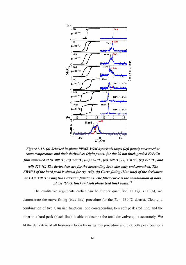
61
Figure 3.11. (a) Selected in-plane PPMS-VSM hysteresis loops (left panel) measured at room temperature and their derivatives (right panel) for the 20 nm thick graded FePtCu
film annealed at (i) 300 °C, (ii) 320 °C, (iii) 330 °C, (iv) 340 °C, (v) 370 °C, (vi) 475 °C, and
(vii) 525 °C. The derivatives are for the descending branches only and smoothed. The FWHM of the hard peak is shown for (v)–(vii). (b) Curve fitting (blue line) of the derivative
at TA = 330 °C using two Gaussian functions. The fitted curve is the combination of hard phase (black line) and soft phase (red line) peaks.74
The qualitative arguments earlier can be further quantified. In Fig. 3.11 (b), we
demonstrate the curve fitting (blue line) procedure for the TA = 330 °C dataset. Clearly, a
combination of two Gaussian functions, one corresponding to a soft peak (red line) and the
other to a hard peak (black line), is able to describe the total derivative quite accurately. We
fit the derivative of all hysteresis loops by using this procedure and plot both peak positions

62
and HC as a function of TA in Fig. 3.12. It is interesting to note that while the saturation
magnetization (MS) (inset of Fig. 3.12) monotonically decreases with increasing TA, the
behavior of the hard/soft peak positions and HC shows a much more complicated and
nonmonotonic behavior. The decrease in MS indicates an overall increasing volume fraction of
the high-Ku L10 phase with TA.10 However, the peak positions in the derivatives, associated
with the reversal of soft and hard phase portions of the film, can be used to interpret how the
A1/L10 phases are actually distributed through the film thickness.
Figure 3.12. TA dependence of the film coercivity (blue triangles) and peak positions of the reversal of the soft (red circles) and hard (black squares) phases. The inset shows the
saturation magnetization (MS) vs TA.74
The depth-dependent anisotropy variation is schematically shown in Fig.3.13 (a)–(f)
for each of the significant TA regions in Fig. 3.13. The lengths of the arrows represent the
strength of the L10-Ku in different parts of the sample. For low TA (300 °C – 310 °C) [see Fig.
3.13 (a)], only the single soft peak appears, corresponding to the dominant, as-deposited, A1
phase. However, already at TA = 320 °C, the single soft peak develops into both hard and soft
peaks, and HC lies at a position in between the field values for these two peaks. TA = 320 °C
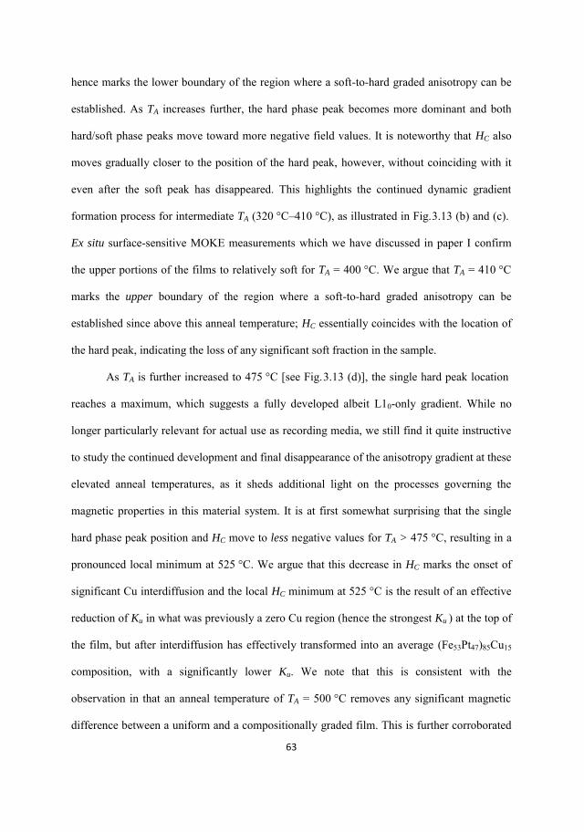
63
hence marks the lower boundary of the region where a soft-to-hard graded anisotropy can be
established. As TA increases further, the hard phase peak becomes more dominant and both
hard/soft phase peaks move toward more negative field values. It is noteworthy that HC also
moves gradually closer to the position of the hard peak, however, without coinciding with it
even after the soft peak has disappeared. This highlights the continued dynamic gradient
formation process for intermediate TA (320 °C–410 °C), as illustrated in Fig.3.13 (b) and (c).
Ex situ surface-sensitive MOKE measurements which we have discussed in paper I confirm
the upper portions of the films to relatively soft for TA = 400 °C. We argue that TA = 410 °C
marks the upper boundary of the region where a soft-to-hard graded anisotropy can be
established since above this anneal temperature; HC essentially coincides with the location of
the hard peak, indicating the loss of any significant soft fraction in the sample.
As TA is further increased to 475 °C [see Fig.3.13 (d)], the single hard peak location
reaches a maximum, which suggests a fully developed albeit L10-only gradient. While no
longer particularly relevant for actual use as recording media, we still find it quite instructive
to study the continued development and final disappearance of the anisotropy gradient at these
elevated anneal temperatures, as it sheds additional light on the processes governing the
magnetic properties in this material system. It is at first somewhat surprising that the single
hard phase peak position and HC move to less negative values for TA > 475 °C, resulting in a
pronounced local minimum at 525 °C. We argue that this decrease in HC marks the onset of
significant Cu interdiffusion and the local HC minimum at 525 °C is the result of an effective
reduction of Ku in what was previously a zero Cu region (hence the strongest Ku ) at the top of
the film, but after interdiffusion has effectively transformed into an average (Fe53Pt47)85Cu15
composition, with a significantly lower Ku. We note that this is consistent with the
observation in that an anneal temperature of TA = 500 °C removes any significant magnetic
difference between a uniform and a compositionally graded film. This is further corroborated
64
by a 17% reduction in the full-width at half-maximum (FWHM) of the switching distribution
that drops from ∆H = 1.41 kOe at 475 °C to ∆H = 1.17 kOe at 525 °C, consistent with a more
uniform switching process. The subsequent increase in HC, as TA reaches 600 °C [see Fig. 3.13
(f)], is finally due to a better overall L10 ordering and the realization of the maximum
attainable Ku of the now compositionally uniform FePtCu film.
Figure 3.13. Schematics of the evolution of the graded anisotropy and its transformation into a uniform anisotropy at TA = 525 °C. The lengths of the arrows represent the local
strength of the L10 anisotropy.74
3.3 Solution for the STO applied field problem: tilted polarizer
(Paper V)
[Co (0.5 nm) /Pd(1 nm)]5 –NiFe(tNiFe) exchange spring films as shown in Fig. 3.14
were deposited on Si(100) substrates using dc magnetron sputtering. The competition between
the IP shape anisotropy of the NiFe and strong PMA of the [Co/Pd]5 multilayer, results in a

65
significant perpendicular component to the magnetization in the NiFe. We find that the tilt
angle can be easily varied by simply varying the NiFe thickness.
Figure 3.14. Schematics of the exchange spring of Co/Pd-NiFe with thickness of NiFe
variable.
The standard perpendicular magnetic hysteresis loops in Fig. 3.15 for samples with
tNiFe= 0, 3, 5, 7, 10 nm are measured using AGM by applying the magnetic field OOP. As
designed, the Co/Pd multilayer shows strong perpendicular anisotropy with the remanence
(M/MS) ~1. When tNiFe= 3nm, the large remanence indicates that a significant PMA is still
maintained in the Co/Pd-NiFe thin film. Thin NiFe is rigidly coupled to the Co/Pd during
switching. The OOP remanence shows a clearly decrease when tNiFe is above 5 nm. The IP
shape anisotropy begins to be comparable to the PMA of the Co/Pd multilayers as tNiFe
increases.

66
Figure 3.15. Major hysteresis loops measured under OOP magnetic field for selective samples. The remanence (M/Ms) is shown in the inset.
The remanent state MFM images in Fig.3.16, show visible changes at different tNiFe.
tNiFe =0, 3and 5 nm, the MFM images are almost featureless due to large single magnetic
domain at remanence. This is consistent with the high remanence in the major OOP hysteresis
loops, indicating that the magnetization in the NiFe has a significant amount of perpendicular
component. However, at tNiFe= 8 nm, clear contrast start to form in the MFM images. This is
consistent with the reduced OOP remanence, suggesting some tilting of the magnetization
away from the film normal. For tNiFe= 10 nm, the magnetic domains breaks into perpendicular
stripe domains due to a more complex reversal mechanism.
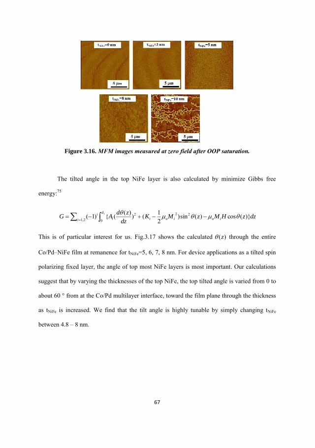
67
Figure 3.16. MFM images measured at zero field after OOP saturation.
The tilted angle in the top NiFe layer is also calculated by minimize Gibbs free
energy:75
This is of particular interest for us. Fig.3.17 shows the calculated )(z through the entire
Co/Pd–NiFe film at remanence for tNiFe=5, 6, 7, 8 nm. For device applications as a tilted spin
polarizing fixed layer, the angle of top most NiFe layers is most important. Our calculations
suggest that by varying the thicknesses of the top NiFe, the top tilted angle is varied from 0 to
about 60 ° from at the Co/Pd multilayer interface, toward the film plane through the thickness
as tNiFe is increased. We find that the tilt angle is highly tunable by simply changing tNiFe
between 4.8 – 8 nm.
id
ioioiii
i dzzHMzMKdz
zdAG
0
2222,1
)(cos)(sin)21())(()1(
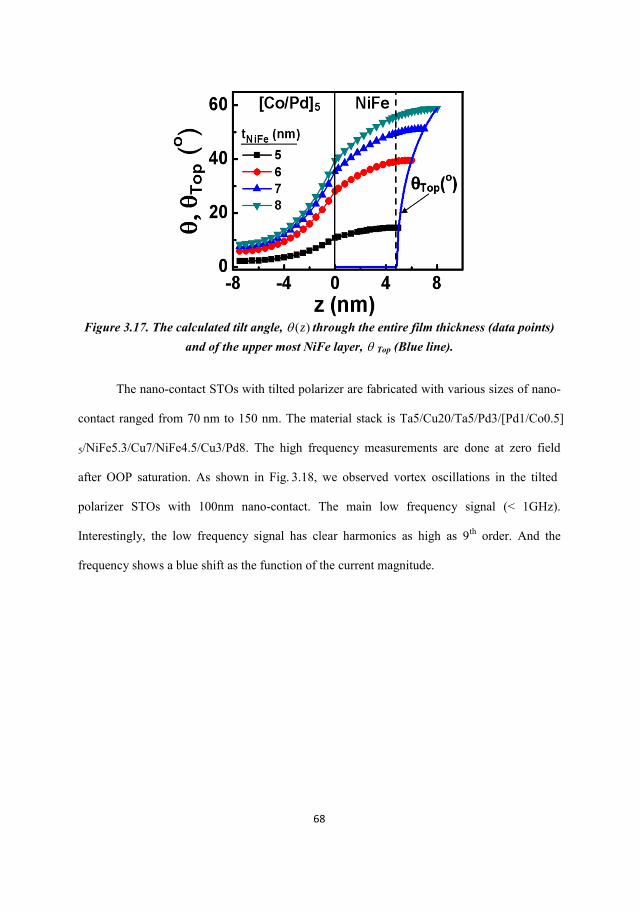
68
Figure 3.17. The calculated tilt angle, )(z through the entire film thickness (data points)
and of the upper most NiFe layer, Top (Blue line).
The nano-contact STOs with tilted polarizer are fabricated with various sizes of nano-
contact ranged from 70 nm to 150 nm. The material stack is Ta5/Cu20/Ta5/Pd3/[Pd1/Co0.5]
5/NiFe5.3/Cu7/NiFe4.5/Cu3/Pd8. The high frequency measurements are done at zero field
after OOP saturation. As shown in Fig. 3.18, we observed vortex oscillations in the tilted
polarizer STOs with 100nm nano-contact. The main low frequency signal (< 1GHz).
Interestingly, the low frequency signal has clear harmonics as high as 9th order. And the
frequency shows a blue shift as the function of the current magnitude.
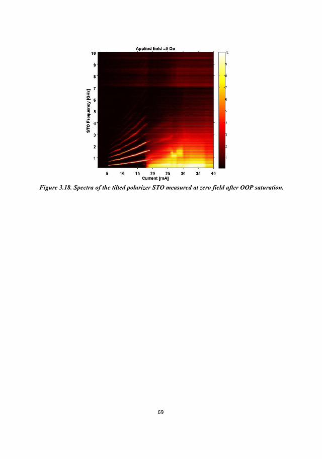
69
Figure 3.18. Spectra of the tilted polarizer STO measured at zero field after OOP saturation.
70
Chapter 4 Conclusions and future works
First, the research work presented in this thesis attempted to use an alternative
approach to increase the magnetic storage capacity. We tried to realize a multi-state storage
bit, instead of simply reducing the size of each memory unit. We have demonstrated that
PSVs whose free and fixed layers have perpendicular magnetic anisotropy have a virtually
continuous range of resistance states that are written by the application of a magnetic field
that partially reverses the free layer magnetization. This information is stored in the remanent
domain state of the free layer. The state is read simply as the resistance of the spin valve.
Thus, these structures have great potential for applications such as field-tunable resistance
trimming devices, memristive devices, or magnetic analog memories with a continuous
number of states per memory cell. In addition to serving as a multi-state memory element, the
PSVs we report here have potential to act as a memristor. Spintronics-based memristors have
been demonstrated with domain wall motion in a free layer induced by spin transfer
torques.76,77 Our PSV devices can be fabricated near a current carrying wire whose Oersted
field acts as the means to tune the domain configuration in the free layer. This wire can be
connected to a patterned PSV to form a two-terminal device whose resistance depends on the
applied current. Additionally, current driven domain wall motion itself could be used to tune
the ratio of up/down domains and therefore the remanent resistance.
The second aim of the thesis is to solve the so-called magnetic recording ‘‘trilemma’’.
We were able to propose and demonstrate a simple procedure to establish a continuous
anisotropy gradient through the thickness of FePtCu films by annealing the films at proper
post annealing temperatures. Important magnetic properties of theses thin films have also
been extensively studied. The analyses of magnetic measurements done by AGM reveal that
the FePtCu film with a well-established anisotropy gradient has a reduced coercivity and

71
moderate thermal stability, which balances the writability and the thermal stability of the
magnetic recording ‘‘trilemma’’. This is potentially very useful for hard disk drives industry.
We also attempt to gain deeper insight of the magnetic properties for the graded anisotropy
FePtCu thin film. The reversal mechanisms of graded anisotropy FePtCu films have been
investigated by AGM, MOKE, in-situ PPMS-VSM measurements combined with FORC
techniques. From a fundamental point of view, we have studied how the induced gradient
anisotropy evolves as the function of the post annealing temperatures. This study gives
contributions to magnetic recording ‘‘trilemma’’ as well. We found that TA plays a critical
role in the realization and evolution of the induced anisotropy gradient. We also suggest that
optimization of the soft-to-hard ratio, yielding the best balance between thermal stability and
writability will have to be found in the TA =320 ~ 410 °C region. Future studies should be
focused on trying to realize perpendicular magnetic anisotropy in these types of samples as
well as trying to establish a well-defined grain structure. Then a true prototype magnetic
recording media will be realized.
The third aim of the thesis is to realize zero-field operation for STOs. We found that
Co/Pd-NiFe exchange spring system is an ideal candidate. Due to the competition between the
strong perpendicular anisotropy and the IP shape anisotropy, the magnetization in the top
NiFe is tilted away from the film normal. The angle is highly tunable over a broad range by
simply change the thickness of top NiFe. After systematically studying the tilted polarizer
Co/Pd-NiFe, we then successfully fabricated a series of nano-contact STOs based on Co/Pd-
NiFe fixed layers with appropriate tilted angle. Our high frequency measurements show that
the tilted polarizer STOs exhibit good vortex oscillations under zero field, which needs further
studies in the future.

72
Bibliography
1 G. Binasch, P. Grünberg, F. Saurenbach, and W.Zinn, Phys. Rev. B 39, 4828 (1989).
2 M. N. Baibich, J. M. Broto, A. Fert, F. Nguyen Van Dau, F. Petroff, P. Eitenne, G. Creuzet, A. Friederich, and J. Chazelas, Phys. Rev. Lett. 61, 2472 (1988).
3 B. Dieny, V. S. Speriosu, S. S. P. Parkin, B. A. Gurney, D.R.Wilhoit,, and D. Mauri, Phys. Rev. B 43, 1297 (1991).
4 S. Yuasa, T. Nagahama, A. Fukushima, Y. Suzuki, and K. Ando, Nature Mater. 3, 868 (2004).
5 S. S. P. Parkin, C. Kaiser, A. Panchula, P. M. Rice, B. Hughes, M. Samant, and See-Hun Yang, Nature Mater. 3, 862 (2004).
6 D. Huffman, N. Withheld, A. Heard, and S. Loomis, Phys. Rev. Lett. 64, 19 (1990).
7 A. Fert, Thin Solid Films 517, 2 (2008).
8 P. Grünberg, Rev. Mod. Phys 80, 1531 (2008).
9 J. C. Slonczewski, J. Magn. Magn. Mater. 159, L1 (1996).
10 L. Berger, Phys. Rev. B 54, 9353 (1996).
11 J. Xiao, A. Zangwill, and M. Stiles, Phys. Rev. B 72, 014446 (2005).
12 M .T. Johnson, P. J .H. Bloemen, F .J .A. D. Broeder, and J . J. D. Vries, Rep. Prog. Phys. 59, 1409 (1996).
13 F. J. A. den Broeder, W. Hoving, and P. J .H. Bloemen, J. Magn. Magn. Mater. 93, 562 (1991).
14 B. J. Kirby, J. E. Davies, K. Liu, S. M. Watson, G. T. Zimanyi, R. D. Shull, P. A. Kienzle, and J. A. Borchers, Phys. Rev. B 81, 100405(R) (2010).
15 R. Law, R. Sbiaa, T. Liew, and T. Chong, J. Appl. Phys. 105, 103911 (2009).
16 S. Lee, D. Y. Shin, S. J. Chung, X. Liu, and J. K. Furdyna, Appl. Phys. Lett. 90, 152113 (2007).
17 Y. Fang, R. K. Dumas, T. N. Anh Nguyen, S. M. Mohseni, S. Chung, C. W. Miller, and J. Åkerman, Adv. Func. Mater 23, 1919 (2013).
18 H. J. Richter, IEEE Trans. Magn. 35, 2790 (1999).
19 K. Z. Gao and H. N. Bertram, IEEE Trans. Magn. 38, 3675 (2002).
73
20 J. P. Wang, Nature Mater. 4, 191 (2005).
21 R. H. Victora, IEEE Trans. Magn. 41, 537 (2005).
22 T. W. McDaniel, J.Phys: Cond. Matter: 17, R315 (2005).
23 J. G. Zhu, X. Zhu, and Y. Tang, IEEE Trans. Magn. 44, 125 (2008).
24 D. Suess, Appl. Phy. Lett. 89, 113105 (2006).
25 J. Slonczewski, J. Magn. Magn. Mater. 159, L1 (1996).
26 L. Berger, Phys. Rev. B 54, 9353 (1996).
27 J. A. Katine, F. J. Albert, R. A. Buhrman, E. B. Myers, and D. C. Ralph, Phys. Rev. Lett. 84, 3149 (2000).
28 Z. Zeng, G. Finocchio, B. Zhang, P. Amiri, J. A. Katine, I. N. Krivorotov, Y. Huai, J. Langer, B. Azzerboni, K. L. Wang, and H. Jiang, Sci. Rep 3, 1 (2013).
29 C. Chappert, A. Fert, and F. N. Van Dau, Nature Mater. 6, 813 (2007).
30 J. Z. Sun, D. J. Monsma, D. W. Abraham, M. J. Rooks, and R. H. Koch, Appl. Phy. Lett. 81, 2202 (2002).
31 S. I. Kiselev, J.C. Sankey, I .N. Krivorotov, N.C. Emley, R.J. Schoelkopf, R.A. Buhrman, and D.C. Ralph, Nature 425, 380 (2003).
32 S. Urazhdin, N. Birge, W. Pratt, and J. Bass, Phys. Rev. Lett. 91,146803 (2003).
33 M. Tsoi, A. G. Jansen, J. Bass, W. C. Chiang, V. Tsoi, and P. Wyder, Nature 406, 46 (2000).
34 W. Rippard, M. Pufall, S. Kaka, T. Silva, and S. Russek, Phys. Rev. B 70, 100406(R) (2004).
35 S. Bonetti, P. Muduli, F. Mancoff, and J. Åkerman, Appl. Phys. Lett. 94, 102507 (2009).
36 T. J. Silva and W. H. Rippard, J. Magn. Magn. Mater. 320, 1260 (2008).
37 O. Boulle, V. Cros, J. Grollier, L. G. Pereira, C. Deranlot, F. Petroff, G. Faini, J. Barnaś, and A. Fert, Nature Phys. 3, 492 (2007).
38 D. Houssameddine, U. Ebels, B. Delaët, B. Rodmacq, I. Firastrau, F. Ponthenier, M. Brunet, C. Thirion, J. -P. Michel, L. Prejbeanu-Buda, M. -C. Cyrille, O. Redon, and B. Dieny, Nature Mater. 6, 447 (2007).
39 A. Dussaux, B. Georges, J. Grollier, V. Cros, A.V. Khvalkovskiy, A. Fukushima, M. Konoto, H. Kubota, K. Yakushiji, S. Yuasa, K. A. Zvezdin, K. Ando, and A. Fert, Nat. Commun. 1, 8 (2010).
74
40 G. Finocchio, V. S. Pribiag, L. Torres, R. A. Buhrman, and B. Azzerboni, Appl. Phy. Lett. 96, 102508 (2010).
41 N. Locatelli, V. V. Naletov, J. Grollier, G. de Loubens, V. Cros, C. Deranlot, C. Ulysse, G. Faini, O. Klein, and A. Fert, Appl. Phy. Lett. 98, 062501 (2011).
42 V. Pribiag, G. Finocchio, B. Williams, D. Ralph, and R. Buhrman, Phys. Rev. B 80, 180411(R) (2009).
43 V. S. Pribiag, I. N. Krivorotov, G. D. Fuchs, P. M. Braganca, O. Ozatay, J. C. Sankey, D. C. Ralph, and R. a. Buhrman, Nature Phys. 3, 498 (2007).
44 Y. Zhou, C. L. Zha, S. Bonetti, J. Persson, and J. Åkerman, Appl. Phy. Lett. 92, 262508 (2008).
45 Y. Zhou, C. L. Zha, S. Bonetti, J. Persson, and J. Åkerman, J. Appl. Phys. 105, 07D116 (2009).
46 Y. Zhou, S. Bonetti, C. L Zha, and J. Åkerman, New J. Phys. 11, 103028 (2009).
47 R.-X. Wang, P.-B. He, Q.-H. Liu, Z.-D. Li, A.-L. Pan, B.-S. Zou, and Y.-G. Wang, J. Magn. Magn. Mater. 322, 2264 (2010).
48 R.-X. Wang, P.-B. He, Z.-D. Li, A.-L. Pan, and Q.-H. Liu, J. Appl. Phys. 109, 033905 (2011).
49 P.-B. He, Z.-D. Li, A.-L. Pan, Q.-L. Zhang, Q. Wan, R.-X. Wang, Y.-G. Wang, W.-M. Liu, and B.-S. Zou, J. Appl. Phys. 105, 043908 (2009).
50 P.-B. He, Z.-D. Li, A.-L. Pan, Q. Wan, Q.-L. Zhang, R.-X. Wang, Y.-G. Wang, W.-M. Liu, and B.-S. Zou, Phys. Rev. B 78, 1 (2008).
51 S. Bonetti, P. Muduli, F. Mancoff, and J. Åkerman, Appl. Phys. Lett. 94, 102507 (2009).
52 S. Bonetti, V. Puliafito, G. Consolo, V. Tiberkevich, A. Slavin, and J. Åkerman, Physical Review B 85, 174427 (2012).
53 S. Bonetti, V. Tiberkevich, G. Consolo, G. Finocchio, P. Muduli, F. Mancoff, A. Slavin, and J. Åkerman, Phys. Rev. Lett. 105, 217204 (2010).
54 S. Banerjee, A. Datta, and M .K. Sanyal, Vacuum 60, 371 (2001).
55 P. J. Flanders, J. Appl. Phys. 63, 3940 (1988).
56 S. D. Bader, J. Magn. Magn. Mater. 100, 440 (1991).
57 I. D. Mayergoyz, Phys. Rev. Lett. 56, 1518 (1986).
58 J. E. Davies, J. Wu, C. Leighton, and K. Liu, Phys. Rev. B 72, 134419 (2005).
75
59 J. E. Davies, O. Hellwig, E. E. Fullerton, G. Denbeaux, J. B. Kortright, and K. Liu, Phys. Rev. B 70, 224434 (2004).
60 J. E. Davies, O. Hellwig, E. E. Fullerton, J. S. Jiang, S. D. Bader, K. Liu, and G. T. Zimanyi, Appl. Phy. Lett. 86, 262503 (2005).
61 R. K. Dumas, C. P. Li, I. V. Roshchin, I. K. Schuller, and K. Liu, Phys. Rev. B 75, 134405 (2007).
62 R. K. Dumas, K. Liu, C. P. Li, I. V. Roshchin, and I. K. Schuller, Appl. Phys. Lett. 91, 202501 (2007).
63 C. R. Pike, A. P. Roberts, and K. L. Verosub, J. Appl. Phys. 85, 6660 (1999).
64 D. D. Tang and Y.-J. Lee, Magnetic Memory (Cambridge University Press, New York, 2010).
65 C. B. Rong, D. Li, V. Nandwana, N. Poudyal, Y. Ding, Z. L. Wang, H. Zeng, and J. P. Liu, Adv. Mater. 18, 2984 (2006).
66 T. Maeda, T. Kai, A. Kikitsu, T. Nagase, and J. Akiyama, Appl. Phy. Lett. 80, 2147 (2002).
67 C. L. Zha , R. K. Dumas, Y. Y. Fang, V. Bonanni, J. Nogues, and Johan Åkerman, Appl. Phy. Lett. 97, 182504 (2010).
68 G .T. Zimanyi, J. Appl. Phys. 103, 07F543 (2008).
69 M. P. Sharrock, J. Appl. Phys. 76, 6413 (1994).
70 C. L. Platt, K. W. Wierman, E. B. Svedberg, R. van de Veerdonk, J. K. Howard, a. G. Roy, and D. E. Laughlin, J. Appl. Phys. 92, 6104 (2002).
71 B. J. Kirby, S. M. Watson, J. E. Davies, G. T. Zimanyi, K. Liu, R. D. Shull, and J. A. Borchers, J. Appl. Phys. 105, 07C929 (2009).
72 A. S. Sabau, P. B. Kadolkar, R. B. Dinwiddie, R. D. Ott, and C. A. Blue, Metall. and Mater. Trans.A 38, 788 (2007).
73 V. Bonanni, Y. Fang, R. K. Dumas, C. Zha, S. Bonetti, J. Nogues, and J. Åkerman, Appl. Phy. Lett. 97, 202501 (2010).
74 Y. Fang, R. K. Dumas, C. L. Zha, and Johan Åkerman, IEEE Magn. Lett. 2, 5500104 (2011).
75 G. Asti, M. Ghidini, R. Pellicelli, C. Pernechele, and M. Solzi, Phys. Rev. B 73, 094406 (2006).

76
76 A. Chanthbouala, R. Matsumoto, J. Grollier, V. Cros, A. Anane, A. Fert, A. V. Khvalkovskiy, K. A. Zvezdin, K. Nishimura, Y. Nagamine, H. Maehara, K. Tsunekawa, A. Fukushima, and S. Yuasa, Nature Phys. 7, 626 (2011).
77 X. Wang, Y. Chen, H. Xi, H. Li, and D. Dimitrov, IEEE Elelctron Device Lett. 30, 294 (2009).

77
List of Figures Figure 1.1 (a) Schematic band structure of a ferromagnetic metal showing the energy band spin
splitting. (b) Explanation of the GMR effect: spin-dependent electron scattering and redistribution of
scattering events upon antialignment of magnetizations. Black arrows are the magnetizations of the
ferromagnetic layers. ............................................................................................................................... 3
Figure 1.2. Illustrantion of the magnetization precession....................................................................... 5
Figure 1.3. vs. tCo of Co/Pd multilayer. 13 ............................................................................... 7
Figure 1.4. The schematic highlighting the magnetic recording trilemma. .......................................... 11
Figure 1.5 The schematics of tilted STO (a) and the schematic structure of the tilted polarizer
composed with Co/Pd-NiFe exchange spring system with the magnetization tilted with respect to the
film plane (b). is adjustable by varying the thickness of top NiFe layer. ........................................... 14
Figure 2.1. Schematic of the magnetron sputtering. ............................................................................. 17
Figure 2.2 Schematics of the structure for nano-contact STOs. ........................................................... 18
Figure 2.3 Schematics of the basic components for X-ray diffractormeter. .......................................... 19
Figure 2.4. Bragg’s law (left) and the scattering geometry (right). ...................................................... 22
Figure 2.5. XRR measurement of a 20 nm thick Ta deposited on Si wafer. .......................................... 23
Figure 2.6. Schematic of AFM components. .......................................................................................... 25
Figure 2.7. The distance dependence of tip-substrate interaction. ....................................................... 26
Figure 2.8. Schematic of photodiode work principle. ........................................................................... 27
Figure 2.9. Schematic of constant heigh mode and constant force mode. ............................................. 28
Figure 2.10. A schematic of the conventional VSM with electromagnet. .............................................. 31
Figure 2.11. A schematic of PPMS sample chamber. ........................................................................... 32
Figure 2.12. A Schematic of an alternating gradient magnetometer. ................................................... 34
Figure 2.13. Schematic of the magneto-optic Kerr effect. ..................................................................... 35
Figure 2.14. The typical three configurations for MOKE measurement. .............................................. 36
Figure 2.15. Schematic of the MOKE magneometor............................................................................. 37
Figure 2.16. Family of FORCs for FePt(20nm)/CoFe(7nm) thin filmed measured by AGM with the
magnetic field applied along the film plane. ......................................................................................... 38
Figure 2.17. FORC distributions of the FePt(20nm)/CoFe(7nm) thin film plotted in (a) H, HR
coordinate and (b) HB, HC coordinate................................................................................................ 40
Figure 2.18 Schematics of the four probe measurement. ...................................................................... 41
Figure 2.19. Schematics of the setup for detecting the microwave signal generated by the STOs. ...... 42
Figure 3.1. Schematic of the pseudo spinvalve showing the graded anisotropy free layer on top
separated from the fixed layer on bottom by a Cu spacer (all the thickness is nm) .............................. 43
Figure 3.2. Major hysteresis loop of the structure. ............................................................................... 44
Figure 3.3. (a)The remanent resistance state can be tuned by partially reversing the free layer. The
crosses and open circles show the resistance measured at and remanence, respectively.( b) The
relative resistance change upon removal of the field is on the order of 0.025%.( c) The resistance
states are essentially independent of time once written by applying HR after saturation.17 .................. 45
Figure 3.4 (a) Family of FORCs for the PSV, with the first point of the individual reversal curves
shown by a black dot. (b) The FORC distribution reveals features related to the reversal of the free
layer (area A) and fixed layer (area B).17 ............................................................................................. 46
Figure 3.5. 20 µm × µ20 m MFM images for various HR show the magnetic domain evolution in the
graded free layer. Dark (bright) domains correspond to the up (down) domains. ............................... 47
78
Figure 3.6. Left panel: schematic of the Cu content depth profile in a graded FePtCu film. Right panel:
XRD patterns of (a) uniform and (b) graded FePtCu (20 nm) films annealed at 300, 400, 500 °C. (c)
(111) peak position and (d) in-plane coercivity of the uniform (blue circles) and graded (red squares)
samples as a function of annealing temperature TA.67 ........................................................................... 49
Figure 3.7. In-plane AGM hysteresis loops (top row) and their derivatives (middle row) for uniform
(blue circles) and graded (red squares) FePtCu (20 nm) films annealed at 300 °C (a) and (b), 400 °C
(c) and (d ), and 500 °C (e) and ( f ). The derivatives are of the descending branch only and smoothed.
The vertical arrow in (c) and (d) indicates the initial ........................................................................... 50
Figure 3.8. MOKE (red squares) and AGM (blue circles) hysteresis loops for a graded FePtCu (50 nm)
film annealed at (a) 300 °C and (b) 400 °C, respectively.67 .................................................................. 53
Figure 3.9. Families of FORCs for the graded FePtCu film annealed at 300 °C measured using the (a)
AGM and (c) MOKE, where the first point of each FORC is shown by a dot. The corresponding FORC
distributions are shown in (b) and (d), respectively. The bold FORC in (a) indicates the initial soft
phase portion of the reversal and the dashed circle and solid oval highlight the soft and hard portions
of the reversal, respectively.73 ............................................................................................................... 57
Figure 3.10. SFDs of the FePtCu film annealed at (a, b) 300 and (c, d) 400 °C calculated from (a, c)
AGM and (b, d) MOKE measurements. The DCD-SFDs (solid and open squares) are calculated by
taking the derivative of the DCD curve. The FORC-SFDs (solid and open circles) are the projection of
the corresponding FORC distributions onto the HR-axis. The arrow in (a) indicates the small peak
discussed in the text. All distributions are normalized by their maximum values.73 ............................. 58
Figure 3.11. (a) Selected in-plane PPMS-VSM hysteresis loops (left panel) measured at room
temperature and their derivatives (right panel) for the 20 nm thick graded FePtCu film annealed at (i)
300 C, (ii) 320 C, (iii) 330 C, (iv) 340 C, (v) 370 C, (vi) 475 C, and (vii) 525 C. The derivatives
are for the descending branches only and smoothed. The FWHM of the hard peak is shown for (v)–
(vii). (b) Curve fitting (blue line) of the derivative at TA = 330 C using two Gaussian functions. The
fitted curve is the combination of hard phase (black line) and soft phase (red line) peaks.74 ............... 61
Figure 3.12. TA dependence of the film coercivity (blue triangles) and peak positions of the reversal of
the soft (red circles) and hard (black squares) phases. The inset shows the saturation magnetization
(MS) vs TA.74 ........................................................................................................................................... 62
Figure 3.13. Schematics of the evolution of the graded anisotropy and its transformation into a
uniform anisotropy at TA = 525 C. The lengths of the arrows represent the local strength of the L10
anisotropy. ............................................................................................................................................. 64
Figure 3.14. Schematics of the exchange spring of Co/Pd-NiFe with thickness of NiFe variable........ 65
Figure 3.15. Major hysteresis loops measured under OOP magnetic field for selective samples. The
remanence (M/Ms) is shown in the inset. ............................................................................................... 66
Figure 3.16. MFM images measured at zero field after OOP saturation.............................................. 67
Figure 3.17. The calculated tilt angle, )(z through the entire film thickness (data points) and of the
upper most NiFe layer, Top (Blue line). .............................................................................................. 68
Figure 3.18. Spectra of the tilted polarizer STO measured at zero field after OOP saturation. .......... 69