ma15500ma15501 industrial analog current voltage-output conditioners · 2015-11-04 · industrial...
TRANSCRIPT

Industrial Analog Current/ Voltage-Output Conditioners
MAX15500/MAX15501
EVALUATION KIT AVAILABLE
General DescriptionThe MAX15500/MAX15501 analog output conditioners provide a programmable current up to Q24mA, or a volt-age up to Q12V proportional to a control voltage signal. The control voltage is typically supplied by an external DAC with an output voltage range of 0 to 4.096V for the MAX15500 and 0 to 2.5V for the MAX15501. The output current and voltage are selectable as either unipolar or bipolar. In the unipolar configuration, a control voltage of 5% full-scale (FS) produces a nominal output of 0A or 0V to achieve underrange capability. A control voltage of 100%FS produces one of two programmable levels (105%FS or 120%FS) to achieve overrange capability. The outputs of the MAX15500/MAX15501 are protected against overcurrent conditions and a short to ground or supply voltages up to Q35V. The devices also monitor for overtemperature and supply brownout conditions. The supply brownout threshold is programmable.
The MAX15500/MAX15501 are programmed through an SPIK interface capable of daisy-chained operation. The MAX15500/MAX15501 provide extensive error reporting through the SPI interface and an additional open-drain interrupt output. The devices include an analog output to monitor load conditions.
The MAX15500/MAX15501 operate over the -40NC to +105NC temperature range. The devices are available in a 32-pin, 5mm x 5mm TQFN package.
ApplicationsProgrammable Logic Controllers (PLCs)Distributed I/OsEmbedded SystemsIndustrial Control and Automation
FeaturesS Supply Voltage Up to Q32.5VS Output Protected Up to Q35VS Programmable Output (Plus Overrange) ±10V
0 to 10V 0 to 5V ±20mA 0 to 20mA 4 to 20mA
S Current Output Drives 0 to 1kIS Voltage Output Drives Loads Down to 1kIS HART CompliantS 2ppm Gain Error Drift Over TemperatureS SPI Interface, with Daisy-Chain CapabilityS Supports +4.096V (MAX15500) or +2.5V
(MAX15501) Full-Scale Input SignalsS Extensive Error Reporting
Short-Circuit and Overcurrent Protection Open-Circuit Detection Brownout Detection Overtemperature Protection
S Fast, 40µs Settling Time
19-4602; Rev 2; 10/15
Ordering Information
Note: All devices are specified over the -40NC to +105NC operating temperature range.+Denotes a lead(Pb)-free/RoHS-compliant package.*EP = Exposed pad.
SPI is a trademark of Motorola, Inc.
SPIINTERFACE
DINSCLK
CS1DOUT
READY
ERROR
MON
REFIN
AIN
DVDD
AVSS
AVDD
FSMODE FSSEL AGND DGND
OUT
SENSERN
COMPCS2
OUTDISAVSSO
AVDDO
ERRORHANDLING
BIDIRECTIONALCURRENTDRIVER
BIDIRECTIONALVOLTAGEDRIVER
ERRORHANDLING
OVER-CURRENT
PROTECTION
SENSERP
SENSEVP
SENSEVN
MAX15500MAX15501
Pin Configuration
MAX15500MAX15501
TQFN
TOP VIEW
29
30
28
27
12
11
13
DIN
READ
Y
ERRO
R
DVDD
DGND
14
SCLK
SENS
EVN
SENS
ERP
AVDD
O
N.C.
OUT
COM
P
1 2
AVSS
4 5 6 7
2324 22 20 19 18
MON
CS1
AIN
REFIN
AGND
FSMODE
DOUT
SENS
ERN
3
21
31 10CS2 FSSEL
32 9N.C. OUTDIS
EP*+
*EXPOSED PAD.
AGND
26 15 AGNDAVDD
25 16 N.C.
N.C.
AVSS
O
8
17
SENSEVP
Simplified Block Diagram
PART PIN-PACKAGE REFERENCE
MAX15500GTJ+ 32 TQFN-EP* +4.096V
MAX15500KGTJ+ 32 TQFN-EP* +4.096V
MAX15501GTJ+ 32 TQFN-EP* +2.5V
MAX15501KGTJ+ 32 TQFN-EP* +2.5V

2 Maxim Integrated
Industrial Analog Current/ Voltage-Output Conditioners
MAX15500/MAX15501
Stresses beyond those listed under “Absolute Maximum Ratings” may cause permanent damage to the device. These are stress ratings only, and functional operation of the device at these or any other conditions beyond those indicated in the operational sections of the specifications is not implied. Exposure to absolute maximum rating conditions for extended periods may affect device reliability.
AVDD to AGND .....................................................-0.3V to +35VAVSS to AGND ......................................................-35V to +0.3VAVDD to AVSS ............................................................. 0 to +70VAVDD to AVDDO ........................................................... 0 to +4VAVSS to AVSSO ............................................................ -4V to 0VDGND to AGND ...................................................-0.3V to +0.3VAVDD to DVDD .........................................................-6V to +35VDVDD to DGND ....................................................-0.3V to +6.0VCS1, CS2, SCLK, DIN, DOUT, READY, ERROR, FSMODE, MON, OUTDIS, FSSEL to DGND ......................-0.3V to +6.0VAIN, REFIN to AGND ............................................-0.3V to +6.0V
SENSEVP, SENSEVN, SENSERP, SENSERN to AGND the higher of -35V and (VAVSS - 0.3V) to
the lower of (VAVDD + 0.3V) and +35VOUT, COMP to AGND .. the higher of -35V and (VAVSS - 0.3V) to
the lower of (VAVDD + 0.3V) and +35VMaximum Current on Pin ............................................... ±100mAContinuous Power Dissipation (derate 34.5mW/NC above +70NC) 32-Pin TQFN (TA = +70NC, multilayer board) .........2758.6mWOperating Temperature Range ........................ -40NC to +105NCStorage Temperature Range ............................ -65NC to +150NCLead Temperature (soldering, 10s) ................................+300NCSoldering Temperature (reflow) ......................................+260NC
ABSOLUTE MAXIMUM RATINGS
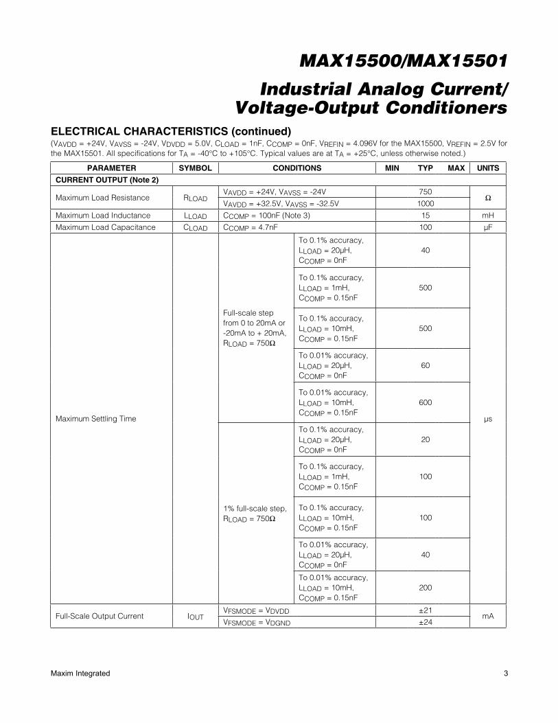
ELECTRICAL CHARACTERISTICS(VAVDD = +24V, VAVSS = -24V, VDVDD = 5.0V, CLOAD = 1nF, CCOMP = 0nF, VREFIN = 4.096V for the MAX15500, VREFIN = 2.5V for the MAX15501. All specifications for TA = -40NC to +105NC. Typical values are at TA = +25NC, unless otherwise noted.)
PARAMETER SYMBOL CONDITIONS MIN TYP MAX UNITS
POWER SUPPLY (Note 1)
Analog Positive Supply Voltage VAVDD5% overrange (FSMODE = DVDD) 15 24 32.5
V20% overrange (FSMODE = DGND) 18.5 24 32.5
Analog Negative Supply Voltage
VAVSS5% overrange (FSMODE = DVDD) -32.5 -24 -15
V20% overrange (FSMODE = DGND) -32.5 -24 -18.5
AVDD to AVDDO Voltage Difference
VAVDDO (Note 1) 2.5 V
AVSS to AVSSO Voltage Difference
VAVSSO (Note 1) 2.5 V
Digital Supply Voltage VDVDD 2.7 5.25 V
Analog Positive Supply Current IAP IAP = IAVDD + IAVDDO, ILOAD = 0A 5 7 mA
Analog Negative Supply Current IAN IAN = IAVSS + IAVSSO, ILOAD = 0A -7 -4.5 mA
Digital Supply Current IDVDD VDVDD = 5V 0.1 0.4 mA
Analog Positive Standby Current ISTBYPISTBYP = IAVDD + IAVDDO, OUTDIS = DGND or software standby mode
1 mA
Analog Negative Standby Current ISTBYNISTBYN = IAVSS + IAVSSO, OUTDIS = DGND or software standby mode
-0.5 mA
ANALOG INPUT (AIN, REFIN)
Input Impedance RIN 10 kI
Input Capacitance CIN 10 pF
Analog Input Full Scale VAINFSSEL = DVDD, MAX15500 4.0 4.096 4.2
VFSSEL = DGND, MAX15501 2.4 2.5 2.6
REFIN Full-Scale Input VREFINFSSEL = DVDD, MAX15500 4.0 4.096 4.2
VFSSEL = DGND, MAX15501 2.4 2.5 2.6
3Maxim Integrated
Industrial Analog Current/ Voltage-Output Conditioners
MAX15500/MAX15501
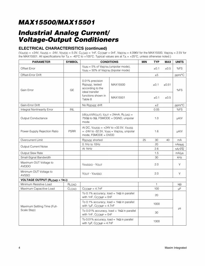
ELECTRICAL CHARACTERISTICS (continued)(VAVDD = +24V, VAVSS = -24V, VDVDD = 5.0V, CLOAD = 1nF, CCOMP = 0nF, VREFIN = 4.096V for the MAX15500, VREFIN = 2.5V for the MAX15501. All specifications for TA = -40NC to +105NC. Typical values are at TA = +25NC, unless otherwise noted.)
PARAMETER SYMBOL CONDITIONS MIN TYP MAX UNITS
CURRENT OUTPUT (Note 2)
Maximum Load Resistance RLOADVAVDD = +24V, VAVSS = -24V 750
IVAVDD = +32.5V, VAVSS = -32.5V 1000
Maximum Load Inductance LLOAD CCOMP = 100nF (Note 3) 15 mH
Maximum Load Capacitance CLOAD CCOMP = 4.7nF 100 FF
Maximum Settling Time
Full-scale step from 0 to 20mA or -20mA to + 20mA, RLOAD = 750I
To 0.1% accuracy, LLOAD = 20FH, CCOMP = 0nF
40
Fs
To 0.1% accuracy, LLOAD = 1mH, CCOMP = 0.15nF
500
To 0.1% accuracy, LLOAD = 10mH, CCOMP = 0.15nF
500
To 0.01% accuracy, LLOAD = 20FH, CCOMP = 0nF
60
To 0.01% accuracy, LLOAD = 10mH, CCOMP = 0.15nF
600
1% full-scale step, RLOAD = 750I
To 0.1% accuracy, LLOAD = 20FH, CCOMP = 0nF
20
To 0.1% accuracy, LLOAD = 1mH, CCOMP = 0.15nF
100
To 0.1% accuracy, LLOAD = 10mH, CCOMP = 0.15nF
100
To 0.01% accuracy, LLOAD = 20FH, CCOMP = 0nF
40
To 0.01% accuracy, LLOAD = 10mH, CCOMP = 0.15nF
200
Full-Scale Output Current IOUTVFSMODE = VDVDD Q21
mAVFSMODE = VDGND Q24
4 Maxim Integrated
Industrial Analog Current/ Voltage-Output Conditioners
MAX15500/MAX15501
ELECTRICAL CHARACTERISTICS (continued)(VAVDD = +24V, VAVSS = -24V, VDVDD = 5.0V, CLOAD = 1nF, CCOMP = 0nF, VREFIN = 4.096V for the MAX15500, VREFIN = 2.5V for the MAX15501. All specifications for TA = -40NC to +105NC. Typical values are at TA = +25NC, unless otherwise noted.)
PARAMETER SYMBOL CONDITIONS MIN TYP MAX UNITS
Offset ErrorVAIN = 5% of VREFIN (unipolar mode), VAIN = 50% of VREFIN (bipolar mode)
Q0.1 Q0.5 %FS
Offset-Error Drift Q5 ppm/NC
Gain Error GE
0.01% precision RSENSE, tested according to the ideal transfer functions shown in Table 8
MAX15500 Q0.1 Q0.51
%FS
MAX15501 Q0.1 Q0.5
Gain-Error Drift No RSENSE drift Q2 ppm/NC
Integral Nonlinearity Error INL 0.05 %FS
Output Conductance(dIOUT/dVOUT), IOUT = 24mA, RLOAD = 750I to 0I, FSMODE = DGND, unipolar mode
1.0 FA/V
Power-Supply Rejection Ratio PSRRAt DC, VAVDD = +24V to +32.5V, VAVSS = -24V to -32.5V, VAIN = VREFIN, unipolar mode, FSMODE = DVDD
1.6 FA/V
Overcurrent Limit RSENSE shorted 25 30 40 mA
Output Current Noise0.1Hz to 10Hz 20 nARMS
At 1kHz 2.6 nA/√HzOutput Slew Rate 1.5 mA/Fs
Small-Signal Bandwidth 30 kHz
Maximum OUT Voltage to AVDDO
VAVDDO - VOUT 2.0 V
Minimum OUT Voltage to AVSSO
VOUT - VAVSSO 2.0 V
VOLTAGE OUTPUT (RLOAD = 1kI)
Minimum Resistive Load RLOAD 1 kI
Maximum Capacitive Load CLOAD CCOMP = 4.7nF 100 FF
Maximum Settling Time (Full-Scale Step)
To 0.1% accuracy, load = 1kI in parallel with 1nF, CCOMP = 0nF
20
Fs
To 0.1% accuracy, load = 1kI in parallel with 1FF, CCOMP = 4.7nF
1000
To 0.01% accuracy, load = 1kI in parallel with 1nF, CCOMP = 0nF
30
To 0.01% accuracy, load = 1kI in parallel with 1FF, CCOMP = 4.7nF
1300

5Maxim Integrated
Industrial Analog Current/ Voltage-Output Conditioners
MAX15500/MAX15501
ELECTRICAL CHARACTERISTICS (continued)(VAVDD = +24V, VAVSS = -24V, VDVDD = 5.0V, CLOAD = 1nF, CCOMP = 0nF, VREFIN = 4.096V for the MAX15500, VREFIN = 2.5V for the MAX15501. All specifications for TA = -40NC to +105NC. Typical values are at TA = +25NC, unless otherwise noted.)
PARAMETER SYMBOL CONDITIONS MIN TYP MAX UNITS
Maximum Settling Time (1% Full-Scale Step)
To 0.1% accuracy, load = 1kI in parallel with 1nF, CCOMP = 0nF
10
Fs
To 0.1% accuracy, load = 1kI in parallel with 1FF, CCOMP = 4.7nF
300
To 0.01% accuracy, load = 1kI in parallel with 1nF, CCOMP = 0nF
20
To 0.01% accuracy, load = 1kI in parallel with 1FF, CCOMP = 4.7nF
600
Gain ErrorTested according to the ideal transfer functions shown in Table 9
Q0.1 Q0.5 %FS
Gain-Error Drift Q2 ppm/NC
Full-Scale Output Voltage VOUT
FSMODE = DVDD5V range 5.25
V10V range 10.5
FSMODE = DGND5V range 6
10V range 12
Offset Error VAIN = 5% of VREFIN (unipolar mode), VAIN = 50% of VREFIN (bipolar mode)
Q0.1 Q0.5 %FS
Offset-Error Drift Q2 ppm/NC
Integral Nonlinearity Error INL 0.05 %FS
Power-Supply Rejection PSRRAt DC, VAVDD = +18.5V to +32.5V, VAVSS = -18.5V to -32.5V, VAIN = VREFIN
30 FV/V
Output-Voltage Noise0.1Hz to 10Hz 16.3 FVRMS
1kHz 250 nV/√HzOutput-Voltage Slew Rate 1.5 V/Fs
Short-Circuit Current 20 30 45 mA
Maximum OUT Voltage to AVDDO
VAVDDO - VOUT 2.0 V
Minimum OUT Voltage to AVSSO
VOUT - VAVSSO 2.0 V

6 Maxim Integrated
Industrial Analog Current/ Voltage-Output Conditioners
MAX15500/MAX15501
ELECTRICAL CHARACTERISTICS (continued)(VAVDD = +24V, VAVSS = -24V, VDVDD = 5.0V, CLOAD = 1nF, CCOMP = 0nF, VREFIN = 4.096V for the MAX15500, VREFIN = 2.5V for the MAX15501. All specifications for TA = -40NC to +105NC. Typical values are at TA = +25NC, unless otherwise noted.)
PARAMETER SYMBOL CONDITIONS MIN TYP MAX UNITS
OUTPUT MONITOR (MON)
Maximum Output Voltage
Current mode, see the Output Monitor section for VMON equations
3
VVoltage mode, see the Output Monitor section for VMON equations
3
Output Resistance 35 kI
OVERTEMPERATURE DETECTION
Overtemperature Threshold +150 NC
Overtemperature Threshold Hysteresis
10 NC
DIGITAL INPUTS (CS1, CS2, SCLK, DIN, OUTDIS, FSSEL, FSMODE)
Input High Voltage VIH 0.7 x
VDVDDV
Input Low Voltage VIL 0.3 x
VDVDDV
Input Hysteresis VIHYST 300 mV
Input Leakage Current IIN VINPUT = 0V or VDVDD Q0.1 Q1.0 FA
Input Capacitance CIN 10 pF
DIGITAL OUTPUT (DOUT, READY)Output Low Voltage VOL ISINK = 4mA 0.4 V
Output High Voltage VOH ISOURCE = 4mAVDVDD -
0.5V
Output Three-State Leakage IOZ DOUT only Q0.1 Q10 FA
Output Three-State Capacitance COZ DOUT only 15 pF
Output Short-Circuit Current IOSS VDVDD = 5.25V Q150 mA
DIGITAL INTERRUPT (ERROR)Interrupt Active Voltage VINT ISINK = 5.0mA 0.4 V
Interrupt Inactive Leakage IINTZ Q0.1 Q1.0 FA
Interrupt Inactive Capacitance CINTZ 15 pF
Interrupt Short-Circuit Current IINTSS VDVDD = 2.7V 5 30 mA
7Maxim Integrated
Industrial Analog Current/ Voltage-Output Conditioners
MAX15500/MAX15501
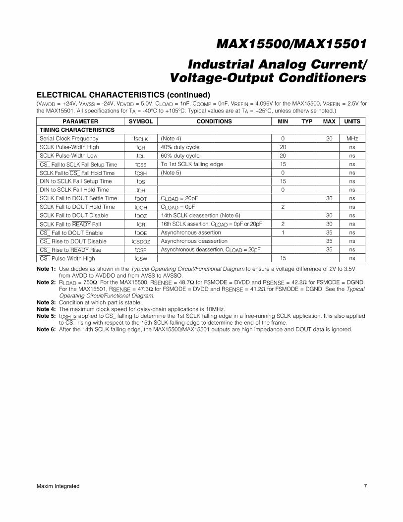
Note 1: Use diodes as shown in the Typical Operating Circuit/Functional Diagram to ensure a voltage difference of 2V to 3.5V from AVDD to AVDDO and from AVSS to AVSSO.
Note 2: RLOAD = 750I. For the MAX15500, RSENSE = 48.7I for FSMODE = DVDD and RSENSE = 42.2I for FSMODE = DGND. For the MAX15501, RSENSE = 47.3I for FSMODE = DVDD and RSENSE = 41.2I for FSMODE = DGND. See the Typical Operating Circuit/Functional Diagram.
Note 3: Condition at which part is stable.Note 4: The maximum clock speed for daisy-chain applications is 10MHz.Note 5: tCSH is applied to CS_ falling to determine the 1st SCLK falling edge in a free-running SCLK application. It is also applied
to CS_ rising with respect to the 15th SCLK falling edge to determine the end of the frame.Note 6: After the 14th SCLK falling edge, the MAX15500/MAX15501 outputs are high impedance and DOUT data is ignored.
ELECTRICAL CHARACTERISTICS (continued)(VAVDD = +24V, VAVSS = -24V, VDVDD = 5.0V, CLOAD = 1nF, CCOMP = 0nF, VREFIN = 4.096V for the MAX15500, VREFIN = 2.5V for the MAX15501. All specifications for TA = -40NC to +105NC. Typical values are at TA = +25NC, unless otherwise noted.)
PARAMETER SYMBOL CONDITIONS MIN TYP MAX UNITS
TIMING CHARACTERISTICS
Serial-Clock Frequency fSCLK (Note 4) 0 20 MHz
SCLK Pulse-Width High tCH 40% duty cycle 20 ns
SCLK Pulse-Width Low tCL 60% duty cycle 20 ns
CS_ Fall to SCLK Fall Setup Time tCSS To 1st SCLK falling edge 15 ns
SCLK Fall to CS_ Fall Hold Time tCSH (Note 5) 0 ns
DIN to SCLK Fall Setup Time tDS 15 ns
DIN to SCLK Fall Hold Time tDH 0 ns
SCLK Fall to DOUT Settle Time tDOT CLOAD = 20pF 30 ns
SCLK Fall to DOUT Hold Time tDOH CLOAD = 0pF 2 ns
SCLK Fall to DOUT Disable tDOZ 14th SCLK deassertion (Note 6) 30 ns
SCLK Fall to READY Fall tCR 16th SCLK assertion, CLOAD = 0pF or 20pF 2 30 ns
CS_ Fall to DOUT Enable tDOE Asynchronous assertion 1 35 ns
CS_ Rise to DOUT Disable tCSDOZ Asynchronous deassertion 35 ns
CS_ Rise to READY Rise tCSR Asynchronous deassertion, CLOAD = 20pF 35 ns
CS_ Pulse-Width High tCSW 15 ns
8 Maxim Integrated
Industrial Analog Current/ Voltage-Output Conditioners
MAX15500/MAX15501
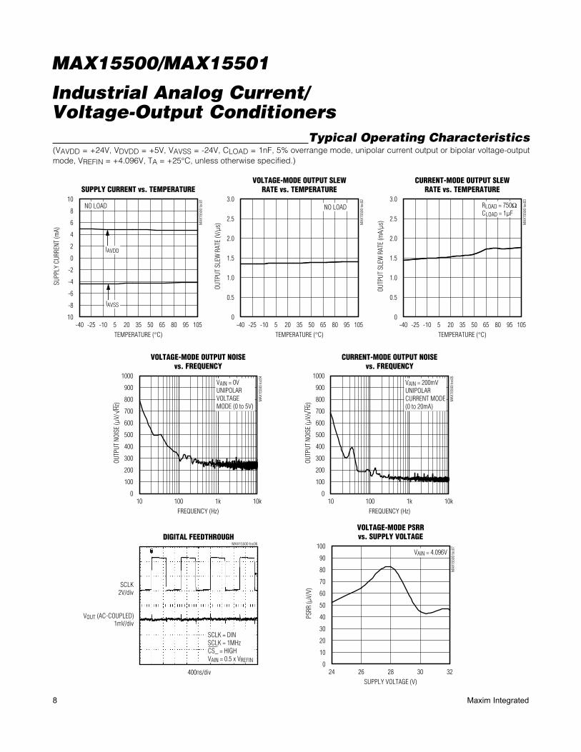
Typical Operating Characteristics(VAVDD = +24V, VDVDD = +5V, VAVSS = -24V, CLOAD = 1nF, 5% overrange mode, unipolar current output or bipolar voltage-output mode, VREFIN = +4.096V, TA = +25NC, unless otherwise specified.)
SUPPLY CURRENT vs. TEMPERATUREM
AX15
500
toc0
1
TEMPERATURE (NC)
SUPP
LY C
URRE
NT (m
A)
958050 65-10 5 20 35-25
-8
-6
-4
-2
0
2
4
6
8
10
10-40 105
IAVDD
IAVSS
NO LOAD
VOLTAGE-MODE OUTPUT SLEWRATE vs. TEMPERATURE
MAX
1550
0 to
c02
TEMPERATURE (NC)
OUTP
UT S
LEW
RAT
E (V
/Fs)
9580655035205-10-25
0.5
1.0
1.5
2.0
2.5
3.0
0-40 105
NO LOAD
CURRENT-MODE OUTPUT SLEWRATE vs. TEMPERATURE
MAX
1550
0 to
c03
TEMPERATURE (NC)
OUTP
UT S
LEW
RAT
E (m
A/F
s)
9580655035205-10-25
0.5
1.0
1.5
2.0
2.5
3.0
0-40 105
RLOAD = 750ICLOAD = 1FF
VOLTAGE-MODE OUTPUT NOISEvs. FREQUENCY
MAX
1550
0 to
c04
FREQUENCY (Hz)
OUTP
UT N
OISE
(FV/
Hz
)
1k100
100
200
300
400
500
600
700
800
900
1000
010 10k
VAIN = 0VUNIPOLARVOLTAGEMODE (0 to 5V)
CURRENT-MODE OUTPUT NOISEvs. FREQUENCY
MAX
1550
0 to
c05
FREQUENCY (Hz)
OUTP
UT N
OISE
(FV/
Hz
)
1k100
100
200
300
400
500
600
700
800
900
1000
010 10k
VAIN = 200mVUNIPOLARCURRENT MODE(0 to 20mA)
MAX15500 toc06
2V/div
VOUT (AC-COUPLED)1mV/div
400ns/div
DIGITAL FEEDTHROUGH
SCLK
SCLK = DINSCLK = 1MHzCS_ = HIGHVAIN = 0.5 x VREFIN
VOLTAGE-MODE PSRRvs. SUPPLY VOLTAGE
MAX
1550
0 to
c07
SUPPLY VOLTAGE (V)
PSRR
(FV/
V)
302826
10
20
30
40
50
60
70
80
90
100
024 32
VAIN = 4.096V

9Maxim Integrated
Industrial Analog Current/ Voltage-Output Conditioners
MAX15500/MAX15501
Typical Operating Characteristics (continued)(VAVDD = +24V, VDVDD = +5V, VAVSS = -24V, CLOAD = 1nF, 5% overrange mode, unipolar current output or bipolar voltage-output mode, VREFIN = +4.096V, TA = +25NC, unless otherwise specified.)
CURRENT-MODE PSRR vs.SUPPLY VOLTAGE
MAX
1550
0 to
c08
SUPPLY VOLTAGE (V)
PSRR
(FA/
V)
313028 2926 2725
0.1
0.2
0.3
0.4
0.5
0.6
0.7
0.8
0.9
1.0
024 32
MAX15500 toc09
VOUT (AC-COUPLED)20mV/div
40Fs/div
LOAD TRANSIENT (VOLTAGE MODE)
IOUT10mA/div
OmA
MAX15500 toc10
IOUT10mA/div
40Fs/div
0mA
LOAD TRANSIENT (CURRENT MODE)
VOUT10V/div
O
FULL-SCALE OUTPUT VOLTAGEvs. TEMPERATURE
MAX
1550
0 to
c11
TEMPERATURE (NC)
FULL
-SCA
LE O
UTPU
T VO
LTAG
E (p
pm/N
C)
958050 65-10 5 20 35-25
-16
-12
-8
-4
0
4
8
12
16
20
-20-40
VAIN = 4.096V
958050 65-10 5 20 35-25-40
OUTPUT CURRENT DRIFTvs. TEMPERATURE
MAX
1550
0 to
c12
TEMPERATURE (NC)
OUTP
UT C
URRE
NT D
RIFT
(ppm
/NC)
-6
-2
2
6
10
-10
VAIN = 4.096V
STANDBY SUPPLY CURRENTvs. TEMPERATURE
MAX
1550
0 to
c13
TEMPERATURE (NC)
SUPP
LY C
URRE
NT (m
A)
9580-25 -10 5 35 5020 65
-1.5
-1.0
-0.5
0
0.5
1.0
1.5
2.0
-2.0-40
IAVDD
IAVSS
NO LOAD

10 Maxim Integrated
Industrial Analog Current/ Voltage-Output Conditioners
MAX15500/MAX15501
Typical Operating Characteristics (continued)(VAVDD = +24V, VDVDD = +5V, VAVSS = -24V, CLOAD = 1nF, 5% overrange mode, unipolar current output or bipolar voltage-output mode, VREFIN = +4.096V, TA = +25NC, unless otherwise specified.)
WAKEUP FROM STANDBY(VOLTAGE MODE)
MAX15500 toc14
50Fs/div
5V/divVOUT
2V/divOUTDIS
0V
0V
FULL-SCALE INPUTBIPOLAR VOLTAGE MODE5% OVERRANGE
MAX15500 toc15
IOUT10mA/div
40Fs/div
WAKEUP FROM STANDBY(CURRENT MODE)
OUTDIS2V/div
GAIN vs. FREQUENCY(HART COMPLIANT)
MAX
1550
0 to
c16
FREQUENCY (Hz)
GAIN
(dB)
10k1k100
-16
-12
-8
-4
0
-2010 100k
UNIPOLARCURRENT MODE
BIPOLARCURRENT MODE
VAIN = 40mVP-P
MAX15500 toc17
IOUT100FA/div
5Fs/div
SMALL-SIGNAL STEP RESPONSE(CURRENT MODE)
VAIN20mV/div
MAX15500 toc18
VOUT(AC-COUPLED)
100mV/div
1Fs/div
SMALL-SIGNAL STEP RESPONSE(VOLTAGE MODE)
VAIN(AC-COUPLED)
50mV/div
OUTPUT SHORT-CIRCUIT CURRENTvs. TEMPERATURE
MAX
1550
0 to
c19
TEMPERATURE (NC)
SHOR
T-CI
RCUI
T CU
RREN
T (m
A)
958050 65-10 5 20 35-25
30.5
31.0
31.5
32.0
32.5
33.0
33.5
34.0
34.5
35.0
30.0-40
VAIN = 4.096V
VOLTAGE-MODE MON TRANSFERCURVE vs. OUTPUT CURRENT
MAX
1550
0 to
c20
IOUT (mA)
MON
(V)
10987654321
1.4
1.8
2.2
2.6
3.0
1.00 11
VAIN = 4.096VNO LOAD ON MON
CURRENT-MODE MON TRANSFERCURVE vs. OUTPUT VOLTAGE
MAX
1550
0 to
c21
VOUT (V)
MON
(V)
1284
1.2
1.4
1.6
1.8
2.0
2.2
2.4
2.6
2.8
3.0
1.00 16
VAIN = 4.096VNO LOAD ON MON
VOLTAGE-MODE MAXIMUM OUT TOAVDDO VOLTAGE vs. TEMPERATURE
MAX
1550
0 to
c22
TEMPERATURE (NC)
MAX
IMUM
INTE
RNAL
VOL
TAGE
DRO
P (V
)
958050 65-10 5 20 35-25
0.1
0.2
0.3
0.4
0.5
0.6
0.7
0.8
0.9
1.0
0-40
VAIN = 4.096V

11Maxim Integrated
Industrial Analog Current/ Voltage-Output Conditioners
MAX15500/MAX15501
Typical Operating Characteristics (continued)(VAVDD = +24V, VDVDD = +5V, VAVSS = -24V, CLOAD = 1nF, 5% overrange mode, unipolar current output or bipolar voltage-output mode, VREFIN = +4.096V, TA = +25NC, unless otherwise specified.)
CURRENT-MODE OUTPUTCONDUCTANCE vs. OUTPUT VOLTAGE
MAX
1550
0 to
c23
OUTPUT VOLTAGE (V)
OUTP
UT C
ONDU
CTAN
CE (F
A/V)
14128 104 62
0.2
0.4
0.6
0.8
1.0
1.2
1.4
1.6
1.8
2.0
00 16
MAX15500 toc24
VOUT5V/div
100Fs/div
LARGE-SIGNAL SETTLING TIME(VOLTAGE MODE, RISING EDGE)
VAIN5V/div
RL = 1kI
CL = 1nF, CCOMP = 0nF
CL = 470nF, CCOMP = 4.7nF
CL = 47nF, CCOMP = 0nF
0
MAX15500 toc25
VOUT5V/div
100Fs/div
LARGE-SIGNAL SETTLING TIME(VOLTAGE MODE, FALLING EDGE)
VAIN5V/div
RL = 1kI
CL = 1nF, CCOMP = 0nF
CL = 470nF, CCOMP = 4.7nF
CL = 47nF, CCOMP = 0nF
MAX15500 toc26
VOUT
10ms/div
LARGE-SIGNAL SETTLING TIME(VOLTAGE MODE, RISING EDGE)
VAIN5V/div
RL = 1kI
CL = 1FF, CCOMP = 4.7nF
CL = 10FF,CCOMP = 4.7nF
CL = 100FF,CCOMP = 4.7nF
MAX15500 toc27
VOUT5V/div
10ms/div
LARGE-SIGNAL SETTLING TIME(VOLTAGE MODE, RISING EDGE)
VAIN5V/div
RL = 1kI
CL = 10FF,CCOMP = 4.7nF
CL = 100FF,CCOMP = 4.7nF
CL = 1FF, CCOMP = 4.7nF
MAX15500 toc28
IOUT4mA/div
200Fs/div
LARGE-SIGNAL SETTLING TIME(CURRENT MODE, RISING EDGE)
VAIN5V/div
RL = 750I
LL = 220FH, CCOMP = 0nF
LL = 1mH, CCOMP = 1nF
LL = 22FH, CCOMP = 0nF
MAX15500 toc29
IOUT4mA/div
200Fs/div
LARGE-SIGNAL SETTLING TIME(CURRENT MODE, FALLING EDGE)
VAIN5V/div
RL = 750I
LL = 220FH, CCOMP = 0nF
LL = 1mH, CCOMP = 1nF
LL = 22FH, CCOMP = 0nF
LARGE-SIGNAL SETTLING TIME(CURRENT MODE, RISING EDGE)
MAX15500 toc30
IOUT4mA/div
20Fs/div
VAIN5V/div
RL = 20I
LL = 220FH,CCOMP = 0.47nF
LL = 1mH, CCOMP = 1nF
LL = 22FH, CCOMP = 0.15nF
LARGE-SIGNAL SETTLING TIME(CURRENT MODE, FALLING EDGE)
MAX15500 toc31
IOUT4mA/div
20Fs/div
VAIN
RL = 20I
LL = 220FH,CCOMP = 0.47nF
LL = 1mH, CCOMP = 1nF
LL = 22FH, CCOMP = 0.15nF
12 Maxim Integrated
Industrial Analog Current/ Voltage-Output Conditioners
MAX15500/MAX15501
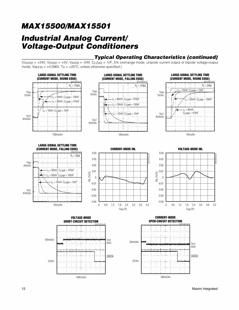
Typical Operating Characteristics (continued)(VAVDD = +24V, VDVDD = +5V, VAVSS = -24V, CLOAD = 1nF, 5% overrange mode, unipolar current output or bipolar voltage-output mode, VREFIN = +4.096V, TA = +25NC, unless otherwise specified.)
CURRENT-MODE INLM
AX15
500
toc3
6
VAIN (V)
INL
(%FS
)
3.63.00.6 1.2 1.8 2.4
-0.03
-0.02
-0.01
0
0.01
0.02
0.03
0.04
-0.040 4.2
VOLTAGE-MODE INL
MAX
1550
0 to
c37
VAIN (V)
INL
(%FS
)
3.63.00.6 1.2 1.8 2.4
-0.03
-0.02
-0.01
0
0.01
0.02
0.03
0.04
-0.040 4.2
LARGE-SIGNAL SETTLING TIME(CURRENT MODE, RISING EDGE)
MAX15500 toc32
IOUT4mA/div
100ms/div
VAIN5V/div
RL = 750I
LL = 80mH, CCOMP = 470nF
LL = 50mH, CCOMP = 100nF
LL = 10mH, CCOMP = 10nF
LARGE-SIGNAL SETTLING TIME(CURRENT MODE, FALLING EDGE)
MAX15500 toc33
IOUT4mA/div
100ms/div
VAIN5V/div
RL = 750I
LL = 50mH, CCOMP = 100nF
LL = 80mH, CCOMP = 470nF
LL = 10mH, CCOMP = 10nF
LARGE-SIGNAL SETTLING TIME(CURRENT MODE, RISING EDGE)
MAX15500 toc34
IOUT4mA/div
10ms/div
VAIN5V/div
RL = 20I
LL = 80mH,CCOMP = 470nF
LL = 50mH, CCOMP = 100nF
LL = 10mH, CCOMP = 10nF
LARGE-SIGNAL SETTLING TIME(CURRENT MODE, FALLING EDGE)
MAX15500 toc35
IOUT4mA/div
10ms/div
VAIN20V/div
LL = 80mH, CCOMP = 470nF
LL = 50mH, CCOMP = 100nF
LL = 10mH, CCOMP = 10nF
RL = 20I
VOLTAGE-MODESHORT-CIRCUIT DETECTION
MAX15500 toc38
100ms/div
2V/div
50mA/div
ERROR
IOUT0mA
CURRENT-MODEOPEN-CIRCUIT DETECTION
MAX15500 toc39
100ms/div
2V/div
50mA/div
ERROR
IOUT0mA
13Maxim Integrated
Industrial Analog Current/ Voltage-Output Conditioners
MAX15500/MAX15501
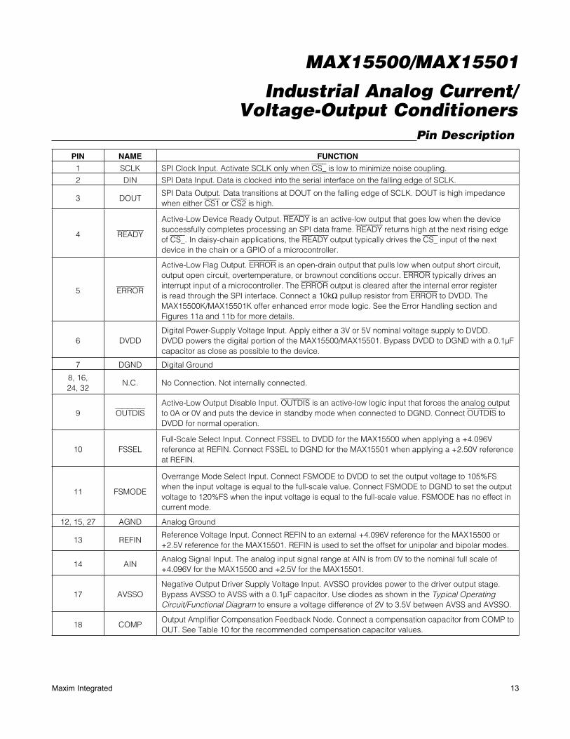
Pin Description
PIN NAME FUNCTION
1 SCLK SPI Clock Input. Activate SCLK only when CS_ is low to minimize noise coupling.
2 DIN SPI Data Input. Data is clocked into the serial interface on the falling edge of SCLK.
3 DOUTSPI Data Output. Data transitions at DOUT on the falling edge of SCLK. DOUT is high impedance when either CS1 or CS2 is high.
4 READY
Active-Low Device Ready Output. READY is an active-low output that goes low when the device successfully completes processing an SPI data frame. READY returns high at the next rising edge of CS_. In daisy-chain applications, the READY output typically drives the CS_ input of the next device in the chain or a GPIO of a microcontroller.
5 ERROR
Active-Low Flag Output. ERROR is an open-drain output that pulls low when output short circuit, output open circuit, overtemperature, or brownout conditions occur. ERROR typically drives an interrupt input of a microcontroller. The ERROR output is cleared after the internal error register is read through the SPI interface. Connect a 10kΩ pullup resistor from ERROR to DVDD. The MAX15500K/MAX15501K offer enhanced error mode logic. See the Error Handling section and Figures 11a and 11b for more details.
6 DVDDDigital Power-Supply Voltage Input. Apply either a 3V or 5V nominal voltage supply to DVDD. DVDD powers the digital portion of the MAX15500/MAX15501. Bypass DVDD to DGND with a 0.1FF capacitor as close as possible to the device.
7 DGND Digital Ground
8, 16, 24, 32
N.C. No Connection. Not internally connected.
9 OUTDISActive-Low Output Disable Input. OUTDIS is an active-low logic input that forces the analog output to 0A or 0V and puts the device in standby mode when connected to DGND. Connect OUTDIS to DVDD for normal operation.
10 FSSELFull-Scale Select Input. Connect FSSEL to DVDD for the MAX15500 when applying a +4.096V reference at REFIN. Connect FSSEL to DGND for the MAX15501 when applying a +2.50V reference at REFIN.
11 FSMODE
Overrange Mode Select Input. Connect FSMODE to DVDD to set the output voltage to 105%FS when the input voltage is equal to the full-scale value. Connect FSMODE to DGND to set the output voltage to 120%FS when the input voltage is equal to the full-scale value. FSMODE has no effect in current mode.
12, 15, 27 AGND Analog Ground
13 REFINReference Voltage Input. Connect REFIN to an external +4.096V reference for the MAX15500 or +2.5V reference for the MAX15501. REFIN is used to set the offset for unipolar and bipolar modes.
14 AINAnalog Signal Input. The analog input signal range at AIN is from 0V to the nominal full scale of +4.096V for the MAX15500 and +2.5V for the MAX15501.
17 AVSSONegative Output Driver Supply Voltage Input. AVSSO provides power to the driver output stage. Bypass AVSSO to AVSS with a 0.1FF capacitor. Use diodes as shown in the Typical Operating Circuit/Functional Diagram to ensure a voltage difference of 2V to 3.5V between AVSS and AVSSO.
18 COMPOutput Amplifier Compensation Feedback Node. Connect a compensation capacitor from COMP to OUT. See Table 10 for the recommended compensation capacitor values.

14 Maxim Integrated
Industrial Analog Current/ Voltage-Output Conditioners
MAX15500/MAX15501
Pin Description (continued)
PIN NAME FUNCTION
19 OUTAnalog Output. The analog voltage or current output range at OUT is programmable. See Tables 1 to 4 for possible output range settings.
20 AVDDO
Positive Output Driver Supply Voltage Input. AVDDO provides power to the driver output stage. Bypass AVDDO to AVDD with a 0.1FF capacitor. Use diodes as shown in the Typical Operating Circuit/Functional Diagram to ensure a voltage difference of 2V to 3.5V between AVDD and AVDDO.
21 SENSERPSense Resistor Positive Connection. See the Typical Operating Circuit/Functional Diagram for the typical connection.
22 SENSERNSense Resistor Negative Connection. See the Typical Operating Circuit/Functional Diagram for the typical connection.
23 SENSEVNKelvin Sense Voltage Negative Input. See the Typical Operating Circuit/Functional Diagram for the typical connection.
25 SENSEVPKelvin Sense Voltage Positive Input. See the Typical Operating Circuit/Functional Diagram for the typical connection.
26 AVDD Positive Analog Supply Voltage Input. Bypass AVDD to AGND with a 0.1FF capacitor.
28 AVSS Negative Analog Supply Voltage Input. Bypass AVSS to AGND with a 0.1FF capacitor.
29 MON Load Monitoring Output. MON provides an analog 0 to 3V output. See the Output Monitor section.
30 CS1 Active-Low SPI Chip-Select Input 1. See the SPI Interface section.
31 CS2 Active-Low SPI Chip-Select Input 2. See the SPI Interface section.
— EPExposed Pad. Internally connected to AVSS. Connect to AVSS. Connect to a large copper area to maximize thermal performance. Do not connect ground or signal lines through EP.

15Maxim Integrated
Industrial Analog Current/ Voltage-Output Conditioners
MAX15500/MAX15501
Typical Operating Circuit/Functional Diagram
10kI
10kI
PGA
OFFSETGENERATOR
DAC
2.5V/4.096VREF
OUTPUT STAGE
SPI INTERFACE/LOGIC I/O
SENSEVP
SENSERP
OUT
SENSERN
SENSEVN
AIN
REFIN
BROWNOUT
TEMPMONITOR
DIN
SCLKCS1CS2
DOUTDVDD
READY OUTD
IS
FSSE
L*
FSM
ODE AGND DGND
MON
AVDD AVDDODVDD
0.1FF0.1FF
0.1FF
POR
CCOMP
RLOAD
RSENSE
COMP
CABLE1
CABLE2
CABLE3
WRITESCLK
CS
READ
GPIO
INT
FC
5V
DVDD
*FSSEL IS CONNECTED TO DGND FOR THE MAX15501.
CLOAD
ADC
24V
AVSS AVSSO
0.1FF
0.1FF
-24V
MAX15500MAX15501
ERROR

16 Maxim Integrated
Industrial Analog Current/ Voltage-Output Conditioners
MAX15500/MAX15501
Detailed DescriptionThe MAX15500/MAX15501 output a programmable current up to Q24mA or a voltage up to Q12V proportional to a control signal at AIN. The devices operate from a dual 15V to 32.5V supply. The control voltage applied at AIN is typically supplied by an external DAC with an output voltage range of 0 to 4.096V for the MAX15500 and 0 to 2.5V for the MAX15501. The MAX15500/MAX15501 are capable of both unipolar and bipolar current and voltage outputs. In current mode, the devices produce currents of -1.2mA to +24mA or -24mA to +24mA. In voltage mode, the devices produce voltages of -0.3V to +6V, -0.6V to +12V, or Q12V. To allow for overrange and underrange capability in unipolar mode, the transfer function of the MAX15500/MAX15501 is offset such that when the voltage at AIN is 5% of full scale, IOUT is 0mA and VOUT is 0V. Once VAIN attains full scale, VOUT or IOUT becomes full scale +5% or +20% depending on the state of FSMODE. The devices are protected against overcurrent and short-circuit conditions when OUT goes to ground or a voltage up to Q32.5V. The devices also monitor for overtemperature and supply brownout conditions. The supply brownout threshold is programmable between ±10V and ±24V in 2V increments.
The MAX15500/MAX15501 are programmed through an SPI interface with daisy-chain capability. A device ready logic output (READY) and two device select inputs (CS1 and CS2) facilitate a daisy-chain arrangement for multiple device applications. The MAX15500/MAX15501 provide
extensive error reporting of short-circuit, open-circuit, brownout, and overtemperature conditions through the SPI interface and an additional open-drain interrupt output (ERROR). The MAX15500/MAX15501 include an analog 0 to 3V output (MON) to monitor the load condition at OUT.
Analog SectionThe MAX15500/MAX15501 support two output modes: current and voltage. Each mode has different full-scale output values depending on the state of FSMODE as detailed in Table 1 through Table 4 and Figures 1 and 2. Use the device configuration register in Table 6 to select the desired voltage or current output range.
StartupDuring startup, the MAX15500/MAX15501 output is set to zero and all register bits are set to zero. The devices remain in standby mode until they are configured through the SPI interface.
Input Voltage RangeThe input voltage full-scale level is selectable between 2.5V and 4.096V using logic input FSSEL. The MAX15500 is specified for a 0 to 4.096V input voltage range, while the MAX15501 is specified for a 0 to 2.500V input volt-age range. Connect FSSEL to DVDD to set the input range to 0 to 4.096V for the MAX15500. Connect FSSEL to DGND to set the input range to 0 to 2.500V for the MAX15501.
Table 1. Output Values for FSMODE = DVDD, Unipolar 5% Overrange
OUTPUT RANGEOUTPUT VALUES
VAIN = 5%FS VAIN = FS
0 to 20mA (4mA to 20mA)
0mA 21mA
0 to 5V 0V 5.25V
0 to 10V 0V 10.5V
Table 2. Output Values for FSMODE = DGND, Unipolar 20% Overrange
OUTPUT RANGEOUTPUT VALUES
VAIN = 5%FS VAIN = FS
0 to 20mA (4mA to 20mA)
0mA 24mA
0 to 5V 0V 6V
0 to 10V 0V 12V
Table 3. Output Values for FSMODE = DVDD, Bipolar 5% Overrange
OUTPUT RANGEOUTPUT VALUES
VAIN = 0V VAIN = FS
Q20mA -21mA +21mA
Q10V -10.5V +10.5V
Table 4. Output Values for FSMODE = DGND, Bipolar 20% Overrange
OUTPUT RANGEOUTPUT VALUES
VAIN = 0V VAIN = FS
Q20mA -24mA +24mA
Q10V -12V +12V

17Maxim Integrated
Industrial Analog Current/ Voltage-Output Conditioners
MAX15500/MAX15501
Output MonitorThe MON output provides an analog voltage signal proportional to the output voltage in current mode and proportional to the output current in voltage mode. Use this signal to measure the system load presented to the output. The full-scale signal on MON is 3V with a typical accuracy of 10%. The signal range is typically 1.5V to 3V in unipolar mode and 0 to 3V in bipolar mode.In current mode, the MAX15500/MAX15501 program IOUT and monitor the voltage at SENSERN.
VMON = 1.425V + (VSENSERN/20)RLOAD = ((VMON - 1.425V) x 20)/IOUT(PROGRAMMED)
In voltage mode, the MAX15500/MAX15501 program VOUT and monitor IOUT.
VMON = 1.521V + 62.4 x ILOADRLOAD = VOUT(PROGRAMMED)/((VMON - 1.521V)/62.4)
Error HandlingMany industrial control systems require error detection and handling. The devices provide extensive error status reporting.An open-drain interrupt flag output, ERROR, pulls low when an error condition is detected. An error register stores the error source. Reading the error register once resets the ERROR pin but not the error register itself, allowing the system to determine the source of the error and take steps to fix the error condition. After the error condition has been fixed, read the error register for the second time to allow the device to clear the error
register. Read the error register for the third time to verify if the error register has been cleared. If another error occurs after the first read, ERROR goes low again. More information on reading and clearing the error register is described in the SPI Interface section.When an output short-circuit or output open-load error occurs and disappears before the error register is read, the intermittent bit is set in the error register. The intermittent bit does not assert for brownout and overtemperature error conditions. The MAX15500/MAX15501 and MAX15500K/MAX15501K offer different error handling for open circuits and short circuits. See the individual sections, Figure 11a, and Figure 11b for more details.
Error ConditionsOutput Short Circuit
The output short-circuit error bit asserts when the output current exceeds 30mA (typ) for longer than 260ms. In current mode, this error occurs when the sense resistor is shorted and the sense voltage is not equal to 0V. In voltage mode, this error occurs when the load is shorted to the supply or ground. The short-circuit error activates the intermittent bit in the error register if the error goes away before the error register is read.
The MAX15500/MAX15501 only asserts the short-circuit flag when a short is detected and an open circuit is not detected.
VAIN
VOUT OR IOUT
FS + 20%
FS + 5%FS
FS5%FS
FSMODE = DGND
FSMODE = DVDD
Figure 1. Unipolar Transfer Function
VAIN
VOUT OR IOUT
FS + 20%
FS + 5%
-FS - 20%
-FS - 5%
FSMODE = DGND
FSMODE = DVDD
50%FS
FS
FS
-FS
Figure 2. Bipolar Transfer Function

18 Maxim Integrated
Industrial Analog Current/ Voltage-Output Conditioners
MAX15500/MAX15501
Output Short-Circuit: Voltage Mode Only (MAX15500K/MAX15501K) The output short-circuit error bit asserts when the output current exceeds 30mA (typ) for longer than 260ms in voltage mode only. This error occurs when the load is shorted to the supply or ground. The short-circuit error activates the intermittent bit in the error register if the error goes away before the error register is read.
Output Open Load (MAX15500/MAX15501)The open-circuit error bit activates when VOUT is within 30mV of AVDDO or AVSSO and there is no short-circuit current in current mode for longer than 260ms. This error activates the intermittent bit in the error register if the error goes away before the error register is read.
The MAX15500/MAX15501 open-circuit flag is active when both a short circuit and open circuit are detected. The MAX15500/MAX15501 does not flag open circuit when the load current is between -3.5mA (typ) to +3.5mA (typ). Figure 11a shows the full range of the open circuit detection range and Figure 11b offers a zoomed in view. The MAX15500/MAX15501 are shown in the red lines.
Output Open Load (MAX15500K/MAX15501K)The open-circuit error bit activates when VOUT is within 30mV of AVDDO or AVSSO for longer than 260ms. This error activates the intermittent bit in the error register if the error goes away before the error register is read.
The MAX15500K/MAX15501K does not flag open circuit when the load current is between -0.5mA (typ) to +0.5mA (typ). Figure 11a shows the full range of the open circuit detection range and Figure 11b offers a zoomed in view. The MAX15500K/MAX15501K are shown in the green lines.
Internal OvertemperatureThe MAX15500/MAX15501 enter standby mode if the die temperature exceeds +150NC and the overtemperature protection is enabled as shown in Table 6. When the die temperature cools down below +140NC, the error regis-ter must be read back twice to resume normal operation. The devices provide a 10NC hysteresis. The MAX15500/MAX15501 and MAX15500K/MAX15501K all trigger the overtemperature ERROR flag in the same manner.
BrownoutThe brownout-error bit activates when the supply voltage (VAVDD or VAVSS) falls below the brownout threshold. The threshold is programmable between Q10V to Q24V in 2V steps. See Table 6 for details. The MAX15500/MAX15501 provide a 2% hysteresis for the brownout threshold. The accuracy of the threshold is typically within 10%. During power-up, ERROR can go low and the brownout register is set. Users need to read out the error register twice to clear all the error register bits and reset ERROR to high. The MAX15500/MAX15501 and MAX15500K/MAX15501K all trigger the overtemperature ERROR flag in the same manner.
Output ProtectionThe MAX15500/MAX15501 supply inputs (AVDD, AVDDO, AVSS, and AVSSO) and sense inputs (SENSERN, SENSERP, SENSEVN, and SENSEVP) are protected against voltages up to Q35V with respect to AGND. See the Typical Operating Circuit/Functional Diagram for the recommended supply-voltage connection.
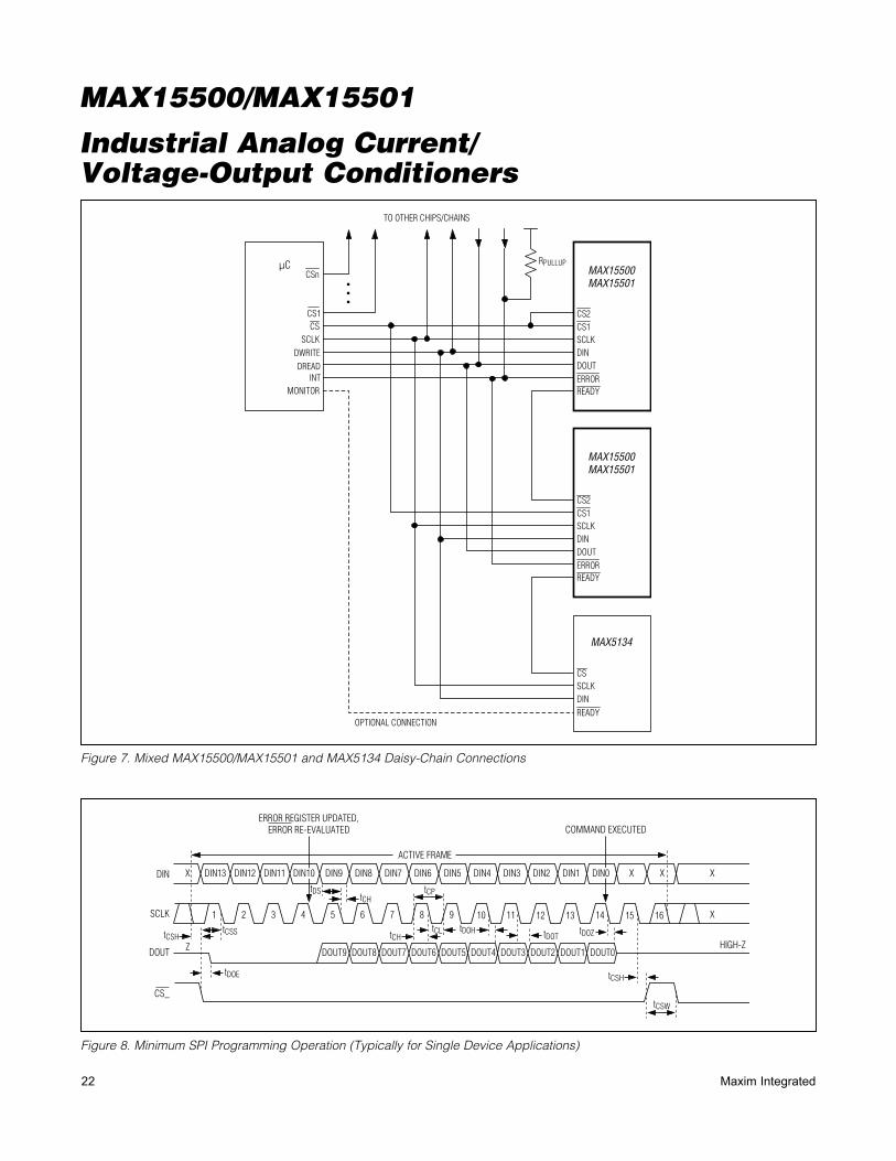
SPI InterfaceStandard SPI ImplementationThe MAX15500/MAX15501 SPI interface supports daisy-chaining. Multiple MAX15500/MAX15501 devices can be controlled from a single 4-wire SPI interface. The MAX15500/MAX15501 feature dual CS_ inputs and an added digital output, READY, that signals when the devices finish processing the SPI frame. CS1 and CS2 are internally OR-ed. Pull both CS1 and CS2 to logic-low to activate the MAX15500/MAX15501. For a daisy-chained application, connect the CS1 input of all of the devices in the chain to the CS driver of the microcontroller. Connect the CS2 input of the first device to ground or to the CS driver of the microcontroller. Connect CS2 of the remaining devices to the READY output of the preceding device in the chain. The READY output of the last device in the chain indicates when all slave devices in the chain are configured. Connect the READY output of the last device in the chain to the microcontroller. Use the open-drain ERROR output as a wired-OR interrupt. See Figures 3 to 6.

19Maxim Integrated
Industrial Analog Current/ Voltage-Output Conditioners
MAX15500/MAX15501
Figure 3. Single Connection (Compatible with Standard SPI)
CS
DWRITE
SCLK
DREAD
CS1
DOUT
SCLKDIN
ERRORINT
FC
CS1
CSn
TO OTHER CHIPS/CHAINS
READYMONITOROPTIONAL CONNECTION
CS2
RPULLUPMAX15500MAX15501
Figure 4. Alternate Single Connection (Compatible with Standard SPI)
Figure 5. Daisy-Chain Connection (Compatible with Standard SPI)
CS
DWRITE
SCLK
DREAD
CS1
DOUT
SCLKDIN
ERRORINT
FC
CS1
CSn
TO OTHER CHIPS/CHAINS
READYMONITOROPTIONAL CONNECTION
CS2
RPULLUP MAX15500MAX15501
CS
DWRITE
SCLK
DREAD
CS1
DOUT
SCLKDIN
ERRORINT
FC
CS1
CSn
TO OTHER CHIPS/CHAINS
READYMONITOR
OPTIONAL CONNECTION
CS2
RPULLUP MAX15500MAX15501
CS1
DOUT
SCLKDIN
ERRORREADY
CS2
MAX15500MAX15501
CS1
DOUT
SCLKDIN
ERRORREADY
CS2
MAX15500MAX15501

20 Maxim Integrated
Industrial Analog Current/ Voltage-Output Conditioners
MAX15500/MAX15501
Modified SPI Interface DescriptionThe SCLK, DIN, and DOUT of the MAX15500/MAX15501 assume standard SPI functionality. While the basic func-tion of the MAX15500/MAX15501 CS_ inputs is similar to the standard SPI interface protocol, the management of the CS_ input within the chain is modified. When both CS_ inputs are low, the MAX15500/MAX15501 assume control of the DOUT line and continue to control the line until the data frame is finished and READY goes low (Figure 9). Once a complete frame is processed and the READY signal is issued, the devices do not accept any data from DIN, until either CS1 or CS2 rises and returns
low. A new communication cycle is initiated by a sub-sequent falling edge on CS1 or CS2. When either CS1 or CS2 is high, the MAX15500/MAX15501 SPI interface deactivates, DOUT returns to a high-impedance mode, READY (if active) clears, and any partial frames not yet processed are ignored.
READY asserts once a valid frame is processed allowing the next device in the chain to begin processing the sub-sequent frame. A valid frame consists of 16 SCLK cycles following the falling edge of CS_. Once READY asserts, it remains asserted until either CS_ rises, completing the programming of the chain.
Figure 6. Daisy-Chain Terminating (Compatible with Standard SPI)
CS
DWRITE
SCLK
DREAD
CS1
DOUT
SCLKDIN
ERRORINT
FC
CS1
CSn
TO OTHER CHIPS/CHAINS
SPI DEVICE
READY
CS2
RPULLUP MAX15500MAX15501
CS1
DOUT
SCLKDIN
ERRORREADY
CS2
MAX15500MAX15501
CS
DOUT
SCLK
DIN
21Maxim Integrated
Industrial Analog Current/ Voltage-Output Conditioners
MAX15500/MAX15501
The MAX15500/MAX15501 relinquish control of DOUT once the devices process the frame(s). DOUT remains high impedance when the SPI interface continues to hold CS_ low beyond the required frame(s). Install a pullup/puldown resistor at the DOUT line to maintain the desired state when DOUT goes high impedance.
Single Device SPI ConnectionFor applications using a single MAX15500 or MAX15501, connect both CS1 and CS2 inputs to the device-select driver of the host microcontroller. Alternatively, connect one of the CS_ inputs to the device-select driver of the host microcontroller and the other CS_ to DGND. Both methods allow standard SPI interface operation. See Figures 3 and 4.
Daisy-Chain SPI ConnectionThe MAX15500/MAX15501-modified SPI interface allows a single SPI master to drive multiple devices in a daisy-chained configuration, saving additional SPI channels for other devices and saving cost in isolated applications.
Figure 5 shows multiple MAX15500/MAX15501 devices connected in a daisy chain. The chain behaves as a single device to the microcontroller in terms of timing with an expanded instruction frame requiring 16 SCLK cycles per device for complete programming. No timing parameters are affected by the READY propagation as all devices connect to the microcontroller chip-select through the CS1 inputs.
A chain of MAX15500/MAX15501 devices can be terminated with any standard SPI-compatible single device without a READY output. The MAX15500/MAX15501 portion of the chain continues to display timing parameters comparable to a single device. See Figure 6.
When using the MAX15500/MAX15501 with mixed chains, the connections could require some modification to accommodate the interfaces of the additional devices in the chain. Construct the daisy chain as shown in Figure 7 when using devices with similar READY outputs but without dual CS_ inputs such as the MAX5134 quad 16-bit DAC. The chain is subject to timing relaxation for parameters given with respect to CS_ rising edges to accommodate READY propagation to and through con-secutive MAX5134 devices.
The chain can begin and terminate with either device type. Each MAX5134 or MAX15500/MAX15501 device in the chain could be replaced by a subchain of similar devices. If the chain is terminated with a standard SPI device, omit the optional connection from READY to the
monitor input on the microcontroller. The MAX15500/MAX15501 portion of the chain continues to display tim-ing parameters comparable to a single device.
SPI Digital Specifications and WaveformsFigures 8, 9, and 10 show the operation of the modified SPI interface. The minimum programming operation typically used in single device applications is 16 SCLK periods, the minimum for a valid frame. This cycle can also represent the operation of the final device in a chain.
The extended programming operation is typically used for devices in daisy-chained applications. In this case, READY drives the chip-select input of the subsequent device in the chain. The next device in the chain begins its active frame on the 16th SCLK falling edge in response to READY falling (latching DIN[13] on the 17th SCLK falling edge, if present).
Aborted SPI OperationsDriving a CS_ input high before a valid SPI frame is transmitted to the device can cause an erroneous com-mand. Avoid driving CS_ high before a valid SPI frame is transmitted to the device. See Figures 9 and 10 for valid SPI operation timing.
SPI Operation DefinitionsInput data bits DIN[13:11] represent the SPI command address while DIN[9:0] represent the data written to or read from the command address. The command address directs subsequent input data to the proper internal register for setting up the behavior of the device and selects the correct status data for readback through DOUT. Command address 0h points to a no-op com-mand and does not impact the operation of the device. DOUT is active during this operation and reads back 00h. Command address 1h points to the configuration register used to program the MAX15500/MAX15501. Device configuration takes effect following the 14th SCLK falling edge. DOUT activates and remains low dur-ing this operation. Command addresses 4h and 5h point to readback commands of the MAX15500/MAX15501. Readback commands provide configuration and error register status through DOUT[9:0] and do not affect the internal operation of the device. Command addresses 2h, 3h, 6h, and 7h are reserved for future use. Table 5 shows the list of commands.
Device Configuration OperationTable 6 shows the function of each bit written to the con-figuration register 1h. Table 7 shows the data readback registers.
22 Maxim Integrated
Industrial Analog Current/ Voltage-Output Conditioners
MAX15500/MAX15501
Figure 7. Mixed MAX15500/MAX15501 and MAX5134 Daisy-Chain Connections
Figure 8. Minimum SPI Programming Operation (Typically for Single Device Applications)
CS
DWRITE
SCLK
DREAD
CS1
DOUT
SCLKDIN
ERRORINT
FC
CS1
CSn
TO OTHER CHIPS/CHAINS
READYMONITOR
OPTIONAL CONNECTION
CS2
RPULLUPMAX15500MAX15501
CS1
DOUT
SCLKDIN
ERRORREADY
CS2
MAX15500MAX15501
SCLKDIN
READY
CS
MAX5134
1 2 3 4 5 6 7 8 9 10 11 12 13 14 15 16
DIN13 DIN12 DIN11 DIN9 DIN8 DIN7 DIN6 DIN5 DIN4 DIN3 DIN2 DIN1X
Z
X X X
X
HIGH-Z
ACTIVE FRAME
CS_
DOUT
SCLK
DIN
tCSH
tCSH
tCSW
tCSS
tDOE
tDOH tDOTtDOZ
tDStCH
tCP
tCLtCH
COMMAND EXECUTED
DIN10 DIN0
DOUT9 DOUT8 DOUT7 DOUT6 DOUT5 DOUT4 DOUT3 DOUT2 DOUT1 DOUT0
ERROR REGISTER UPDATED,ERROR RE-EVALUATED

23Maxim Integrated
Industrial Analog Current/ Voltage-Output Conditioners
MAX15500/MAX15501
Readback OperationsWrite to the command addresses 4h or 5h to read back the configuration register data or the internal error information through DOUT[9:0]. For error readback operations, each bit corresponds to a specific error condition, with multiple bits indicating multiple error conditions present.
Intermittent ErrorsAn intermittent error is defined as an error that is detected and is resolved before the error register is read back. When the error is resolved without intervention, the inter-mittent bit (bit 9) is set. The output short-circuit and output open-load errors trigger the intermittent bit. Internal over-
temperature and supply voltage brownout do not trigger the intermittent bit.
Error Reporting ApplicationsThe ERROR output is typically connected to an inter-rupt input of the system microcontroller. The MAX15500/MAX15501 only issue an interrupt when a new error con-dition is detected. The devices do not issue interrupts when errors (either individual or multiple) are resolved or when already reported errors persist. The system microcontroller resets ERROR when the system micro-controller reads back the error register. ERROR does not assert again unless a different error occurs.
Figure 9. Extended SPI Programming Operation (Daisy-Chained Applications)
Figure 10. Aborted SPI Programming Operation (Invalid, Showing tCSDOZ and Internal Activity)
1 2 3 4 5 6 7 8 9 10 11 12 13 14 15 16 17
DIN13 DIN12 DIN11 DIN9 DIN8 DIN7 DIN6 DIN5 DIN4 DIN3 DIN2 DIN1X
Z
X X X
X
HIGH-Z
ACTIVE FRAME
CS_
DOUT
SCLK
DIN
tCSH
tCSV
tCSR
tCSS
tDOE
tDOH tDOTtDOZ
tDStCH
tCP
tCLtCH
tCR
DIN10 DIN0
DOUT9 DOUT8 DOUT7 DOUT6 DOUT5 DOUT4 DOUT3 DOUT2 DOUT1 DOUT0
READY
1 2 3 4 5 6 7 8 9 10 11 12 13 14 15 16
Z
X
HIGH-Z
CS_
DOUT
SCLK
tCSHtCSS
tDOE tCSDOZ
ERROR REGISTER UPDATED,ERROR RE-EVALUATED
OPERATION ABORTED
DOUT9

24 Maxim Integrated
Industrial Analog Current/ Voltage-Output Conditioners
MAX15500/MAX15501
Figure 11a. Diagram Showing the MAX15500/MAX15501 “Plain” (Red) and the MAX15500K/MAX15501K (Teal) Open-Circuit Detection Windows
Figure 11b. Zoomed In Diagram Showing the MAX15500/MAX15501 “Plain” (Red) and the MAX15500K/MAX15501K (Teal) Open-Circuit Detection Windows

25Maxim Integrated
Industrial Analog Current/ Voltage-Output Conditioners
MAX15500/MAX15501
Table 5. SPI Commands
Table 6. Configuration Register
Note: Modes 2h and 3h are functionally identical.
Table 7. Readback Operations and Formatting
LOCATION FUNCTION DESCRIPTION
DIN[9:7] Mode[2:0]
Sets device operating mode.000 Mode[0]: Standby 100 Mode[4]: Standby001 Mode[1]: Bipolar current: Q20mA 101 Mode[5]: Bipolar voltage: Q10V010 Mode[2]: Unipolar current: 0 to 20mA 110 Mode[6]: Unipolar voltage: 0 to 10V011 Mode[3]: Unipolar current: 4mA to 20mA 111 Mode[7]: Unipolar voltage: 0 to 5V
DIN[6:4] VBOTH[2:0]
Sets supply voltage brownout threshold for error reporting.000: Q10V 100: Q18V001: Q12V 101: Q20V010: Q14V 110: Q22V011: Q16V 111: Q24V
DIN[3]Thermal
shutdown0 = thermal protection off. 1 = thermal protection on.
DIN[10], DIN[2:0]
— Reserved
DOUT BITS DESCRIPTION
COMMAND ADDRESS DIN[13:11] = 101. READBACK DEVICE CONFIGURATION REGISTER
DOUT[9:0] See configuration register details in Table 6.
COMMAND ADDRESS DIN[13:11] = 100. READBACK ERROR REGISTER
DOUT[9] Output Intermittent Fault. For details, see the Error Handling section.
DOUT[8]Output Short Circuit. Output short circuit. In the MAX15500/MAX15501, this bit asserts when IOUT > 30mA in voltage and current modes for longer than 260ms. In the MAX15500K/MAX15501K, this bit asserts when Iout > 30mA for longer than 260ms (in voltage mode only).
DOUT[7]Output Open Load. In the MAX15500/MAX15501, this bit asserts when VOUT is within 30mV of AVDDO or AVSSO and there is no short-circuit condition for longer than 260ms. In the MAX15500K/MAX15501K, the output open load bit asserts when VOUT is within 30mV of AVDDO or AVSSO for longer than 260ms.
DOUT[6] Internal Overtemperature. This bit asserts when the die temperature exceeds +150NC.
DOUT[5] Supply Brownout. This bit asserts when either supply has entered the brownout limits. See Table 6 for details.
DOUT[4:0] Reserved
COMMAND ADDRESSDIN[13:11]
NAME DESCRIPTION
000 No-op No operation.
001 Write configuration Write device configuration register. See Table 6 for details.
010 Reserved Reserved, no operation.
011 Reserved Reserved, no operation.
100 Read error Read error register status. See Table 7 for details.
101 Read configuration Read device configuration register. See Table 6 for details.
110 Reserved Reserved, no operation.
111 Reserved Reserved, no operation.
26 Maxim Integrated
Industrial Analog Current/ Voltage-Output Conditioners
MAX15500/MAX15501
Since the MAX15500/MAX15501 do not use a continuous clock signal, the SPI read cycles are used to cycle the error detection and reporting logic. Continue to poll the device until the error readback reports an all clear status when resolving single or multiple errors. See below for examples of typical error handling situations and the effects of the SPI read operations.
1) Error resolved by the system.
a) The MAX15500/MAX15501 detect an error condi-tion and ERROR asserts.
b) The host controller reads the error register for the first time. This has the effect of resetting ERROR. The data indicates to the host processor which error is active.
c) The host processor resolves the error successfully.
d) The host processor reads the error register for the second time. The data still shows that the error is present as the error persisted for some time after step b and before step c. If the error is either an open load or short circuit, the intermittent bit is set. An overtemperature or a brownout does not set the intermittent bit. Reading the register a second time resets the register.
e) The host reads the error register for a third time. The data now shows the error is resolved and future occurrences of this error will trigger ERROR assertion.
2) Error resolved before the host processor reads error register.
a) The MAX15500/MAX15501 detect an error condi-tion and ERROR asserts, but the error resolves itself.
b) The host controller reads the error register for the first time resetting ERROR. The data indicates to the host processor which error is active. The data also indicates to the host that the error has been resolved since the intermittent bit is set.
c) The host processor reads the error register for the second time. The data still shows that the error is active. If the error is for an output fault, the data also indicates to the host that the error has been resolved since the intermittent bit is set. Reading the register a second time resets the register.
3) An error that cannot be resolved.
a) The MAX15500/MAX15501 detect an error condi-tion and ERROR asserts.
b) The host controller reads the error register for the first time and resets ERROR. The data indicates to the host processor which error is active.
c) The host processor takes action to resolve the error unsuccessfully.
d) The host processor reads the error register for the second time. The data still shows that the error is present.
e) The host processor reads the error for the third time. The data show the error to be unresolved. ERROR does not respond to the same error until the error is resolved and reported. ERROR asserts if different errors occur.
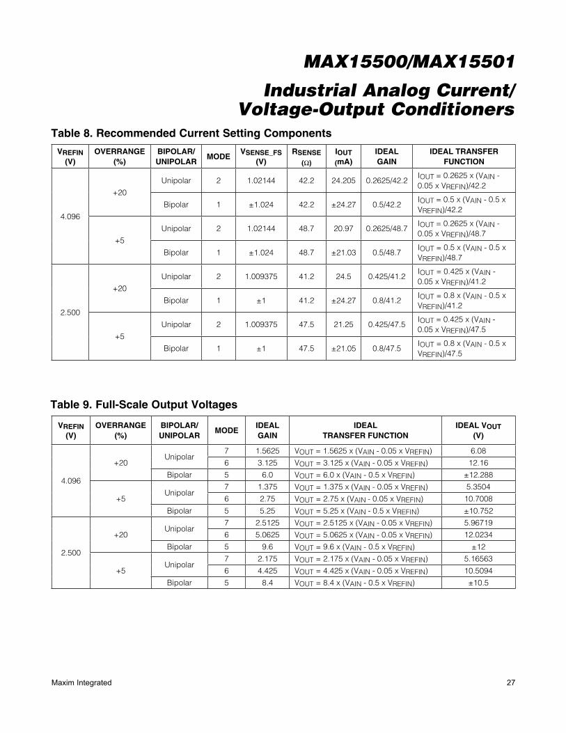
Applications InformationSetting the Output Gain in Current Mode
In current mode, there is approximately 1.0V across the current-sensing resistors at full scale. The current sens-ing resistor sets the gain and is calculated as follows:
RSENSE = VSENSE_FS/IMAX
where VSENSE_FS is the full-scale voltage across the sense resistor.
See Table 8 for values of VSENSE_FS.
Output Gain in Voltage ModeThe output gain in voltage mode is fixed as shown in Table 9.
Selection of the Compensation Capacitor (CCOMP)
Use Table 10 to select the compensation capacitor.
Layout ConsiderationsIn the current-mode application, use Kelvin and a short connection from SENSERN and SENSERP to the RSENSE terminals to minimize gain-error drift. Balance and mini-mize all analog input traces for optimum performance.
27Maxim Integrated
Industrial Analog Current/ Voltage-Output Conditioners
MAX15500/MAX15501
Table 8. Recommended Current Setting Components
Table 9. Full-Scale Output Voltages
VREFIN (V)
OVERRANGE (%)
BIPOLAR/UNIPOLAR
MODEVSENSE_FS
(V)RSENSE
(I)
IOUT (mA)
IDEAL GAIN
IDEAL TRANSFER FUNCTION
4.096
+20
Unipolar 2 1.02144 42.2 24.205 0.2625/42.2IOUT = 0.2625 x (VAIN - 0.05 x VREFIN)/42.2
Bipolar 1 Q1.024 42.2 Q24.27 0.5/42.2IOUT = 0.5 x (VAIN - 0.5 x VREFIN)/42.2
+5
Unipolar 2 1.02144 48.7 20.97 0.2625/48.7IOUT = 0.2625 x (VAIN - 0.05 x VREFIN)/48.7
Bipolar 1 Q1.024 48.7 Q21.03 0.5/48.7IOUT = 0.5 x (VAIN - 0.5 x VREFIN)/48.7
2.500
+20
Unipolar 2 1.009375 41.2 24.5 0.425/41.2IOUT = 0.425 x (VAIN - 0.05 x VREFIN)/41.2
Bipolar 1 Q1 41.2 Q24.27 0.8/41.2IOUT = 0.8 x (VAIN - 0.5 x VREFIN)/41.2
+5
Unipolar 2 1.009375 47.5 21.25 0.425/47.5IOUT = 0.425 x (VAIN - 0.05 x VREFIN)/47.5
Bipolar 1 Q1 47.5 Q21.05 0.8/47.5IOUT = 0.8 x (VAIN - 0.5 x VREFIN)/47.5
VREFIN (V)
OVERRANGE (%)
BIPOLAR/UNIPOLAR
MODEIDEALGAIN
IDEALTRANSFER FUNCTION
IDEAL VOUT (V)
4.096
+20Unipolar
7 1.5625 VOUT = 1.5625 x (VAIN - 0.05 x VREFIN) 6.08
6 3.125 VOUT = 3.125 x (VAIN - 0.05 x VREFIN) 12.16
Bipolar 5 6.0 VOUT = 6.0 x (VAIN - 0.5 x VREFIN) Q12.288
+5Unipolar
7 1.375 VOUT = 1.375 x (VAIN - 0.05 x VREFIN) 5.3504
6 2.75 VOUT = 2.75 x (VAIN - 0.05 x VREFIN) 10.7008
Bipolar 5 5.25 VOUT = 5.25 x (VAIN - 0.5 x VREFIN) Q10.752
2.500
+20Unipolar
7 2.5125 VOUT = 2.5125 x (VAIN - 0.05 x VREFIN) 5.96719
6 5.0625 VOUT = 5.0625 x (VAIN - 0.05 x VREFIN) 12.0234
Bipolar 5 9.6 VOUT = 9.6 x (VAIN - 0.5 x VREFIN) Q12
+5Unipolar
7 2.175 VOUT = 2.175 x (VAIN - 0.05 x VREFIN) 5.16563
6 4.425 VOUT = 4.425 x (VAIN - 0.05 x VREFIN) 10.5094
Bipolar 5 8.4 VOUT = 8.4 x (VAIN - 0.5 x VREFIN) Q10.5

28 Maxim Integrated
Industrial Analog Current/ Voltage-Output Conditioners
MAX15500/MAX15501
Table 10. Recommended Compensation Capacitor for Various Load Conditions
Chip InformationPROCESS: BiCMOS
Package InformationFor the latest package outline information and land patterns (footprints), go to www.maximintegrated.com/packages. Note that a “+”, “#”, or “-” in the package code indicates RoHS status only. Package drawings may show a different suffix character, but the drawing pertains to the package regardless of RoHS status.
CL = Load capacitance.RL = Load resistance.LL = Load inductance.CCOMP = Compensation capacitance.
PACKAGE TYPE
PACKAGE CODE
OUTLINE NO.
LANDPATTERN NO.
32 TQFN-EP T3255+4 21-0140 90-0012
MODE CL (F) RL (kI) LL (H) CCOMP (F)
Voltage 0 to 1n 1 0 0
Voltage 1n to 100n 1 0 1n
Voltage 100n to 1F 1 0 2.2n
Voltage 1F to 100F 1 0 4.7n
Current 0 to 1n 20 to 750 0 to 20F 0
Current 0 to 1n 20 to 750 20F to 1m 2.2n
Current 0 to 1n 20 to 750 1m to 50m 100n
Current 1n to 100n 20 to 750 0 to 20F 1n
Current 1n to 100n 20 to 750 20F to 1m 2.2n
Current 1n to 100n 20 to 750 1m to 50m 100n
Current 100n to 1F 20 to 750 0 to 20F 2.2n
Current 100n to 1F 20 to 750 20F to 1m 2.2n
Current 100n to 1F 20 to 750 1m to 50m 100n
Current 1F to 100F 20 to 750 0 to 20F 2.2n
Current 1F to 100F 20 to 750 20F
to 1m 2.2n
Current 1F to 100F 20 to 750 1m to 50m 100n

Maxim Integrated cannot assume responsibility for use of any circuitry other than circuitry entirely embodied in a Maxim Integrated product. No circuit patent licenses are implied. Maxim Integrated reserves the right to change the circuitry and specifications without notice at any time. The parametric values (min and max limits) shown in the Electrical Characteristics table are guaranteed. Other parametric values quoted in this data sheet are provided for guidance.
Maxim Integrated 160 Rio Robles, San Jose, CA 95134 USA 1-408-601-1000 29© 2015 Maxim Integrated Products, Inc. Maxim Integrated and the Maxim Integrated logo are trademarks of Maxim Integrated Products, Inc.
Industrial Analog Current/ Voltage-Output Conditioners
MAX15500/MAX15501
Revision History
REVISIONNUMBER
REVISION DATE
DESCRIPTIONPAGES
CHANGED
0 7/09 Initial release —
1 2/11 Corrected description of DOUT pin in Pin Description section 13
2 10/15Added new figures and text to Applications section and added “K” versions for added ERROR pin functionality.
1, 13, 17, 18, 23, 24