lx7309 evaluation board user’s guide
TRANSCRIPT

LX7309 EVALUATION BOARD USER GUIDE
Copyright © 2012 Microsemi Page 1 Rev. 1.0 1/24/12 Analog Mixed Signal Group
11861 Western Avenue, Garden Grove, CA. 92841, 714-898-8121, Fax: 714-893-2570
LX7309 EVALUATION BOARD USER’S GUIDE
LX7309 PWM Controller IC

LX7309 EVALUATION BOARD USER GUIDE
Copyright © 2011 Microsemi Page 2 Rev. 1.0 1/24/12 Analog Mixed Signal Group
11861 Western Avenue, Garden Grove, CA. 92841, 714-898-8121, Fax: 714-893-2570
TABLE OF CONTENTS
Overview ..................................................................................................................................................................... 3 LX7309 Overview Evaluation Board Operation PCB Layout Guidelines .............................................................................................................................. 4 TEST CONSIDERATIONS ................................................................................................................................... 8 Evaluation Board TEST Data ....................................................................................................................... 8 TABLES I/O Connection Descriptions .................................................................................................................. 3 FIGURES
LX7309 PCB Critical Traces .................................................................................................................... 4 LX7309 Evaluation Board Silk Screen .................................................................................................... 5 LX7309 Evaluation Board Top Layer ...................................................................................................... 6 LX7309 Evaluation Board Bottom Layer ................................................................................................ 7 LX7309 Evaluation Board Schematic ................................................................................................... 14

LX7309 EVALUATION BOARD USER GUIDE
Copyright © 2011 Microsemi Page 3 Rev. 1.0 1/24/12 Analog Mixed Signal Group
11861 Western Avenue, Garden Grove, CA. 92841, 714-898-8121, Fax: 714-893-2570
OVERVIEW
The LX7309 is a peak current mode control synchronous flyback DC-DC controller. The controller has a number of features designed to improve efficiency and reliability, including:
High Voltage Gate Drivers
Soft Start Circuit
Low Voltage Protection Warning
Over Current Protection
The LX7309 device is housed in a 4mm x 4mm 24 pin plastic QFN package.
EVALUATION BOARD OPERATION
The LX7309 Evaluation Board contains a single LX7309 device and components necessary to provide a 12V 48W isolated output. Two standard Banana Jacks are provided for connecting to a 37V to 57V power source. A 4 pin connector provides the 12V output. Output current is 4A max. The input supply source should be voltage limited to 57V max.
The test point descriptions for the evaluation circuit are summarized in Table 1. Please refer to this table for evaluation board setup.
Table 1 – Evaluation Board I/O Connector and Test Point Reference
Reference Description
J5 37V to 57V power source input (+) connection. Source should be capable of 1.6A continuous current
J6 37V to 57V power source input (-) connection. Source should be capable of 1.6A continuous current
J1 12V output connection. Maximum output power is 4 Amps.
J2 VIN_SEL selection. J2 installed configures the LX7309 to operate with VIN UVLO. With J2 not installed Power Fail Warning (PFW) is enabled. See LX7309 datasheet for details. It is recommended to operate this evaluation board with J2 installed.
TP1 VIN (+) monitor. Used as a monitor point for VIN+.
TP6 VIN (-) monitor. Used as a monitor point for VIN-.
TP3 VCC monitor. Used as a monitor point for VCC. Referenced to Primary Ground.
TP4 Primary Switch Node monitor. Used as a monitor point for the Primary Switch Drain connection. Referenced to Primary Ground.
TP2 & TP5
Optional Inputs for Network Analyzer. Used to generate Bode Plots. TP2 can be used to monitor the regulated output voltage before the post LC filter. This signal is referenced to Secondary Ground.
TP7 Power Fail Warning (PFW) monitor. Used when J2 is not installed. Referenced to Primary Ground.
TP8 SG output monitor. Used to monitor gate drive signal to synchronous FET drive isolation transformer. Referenced to Primary Ground
TP9 LX7309 SYNC input. A 5V peak signal with frequency set to 2 x the free-running frequency can be used to synchronize the LX7309’s internal oscillator to an external clock. Pulse width should be 200ns max. Referenced to Primary Ground.
TP10 LX7309 ENABLE pin input. Pulled up to LX7309 VDD through a 100K resistor. Connect to Primary Ground to disable the LX7309.
TP11 Primary Ground. Used for scope probes and measurement terminations. Should not be used as a power ground connection.

LX7309 EVALUATION BOARD USER GUIDE
Copyright © 2011 Microsemi Page 4 Rev. 1.0 1/24/12 Analog Mixed Signal Group
11861 Western Avenue, Garden Grove, CA. 92841, 714-898-8121, Fax: 714-893-2570
PCB LAYOUT GUIDELINES
When laying out the PCB, consideration of high current paths is required, in particular the primary-side high current paths from the input filter capacitors (C2 – C5, C20) to the transformer primary, the transformer primary to the primary switch transistor (Q2), the primary switch transistor’s source current path to the current sense resistor (R9), and the sense resistor’s current path back to the input filter capacitor’s connection to ground. These critical current paths should be on a single layer only and not be established on multiple layers through vias. Establishing these traces along with their associated parts on the top layer is preferred, both electrically and thermally.
Equally, the secondary-side high current paths should be given the same consideration, with wide, heavy traces ran on a single layer only with no vias interrupting the current flow. These would include the current path from the transformer secondary to the output filter capacitors (C7 & C8), the transformer secondary to the synchronous rectifier (Q1), and the synchronous rectifier (Q1) ground current path back to the output filter capacitors (C7 & C8). The top layer is preferred for both the components and high current traces.
The high current ground should connect separately to the LX7309’s pin 20, preferably on the top layer and unbroken by vias. Pin 20 is the return for the PG and SG gate drive circuits; a clean current path between this pin and the primary transistor return is essential.
The LX7309 and associated signal-level circuitry should utilize a separate signal ground common to pin 17. The VDD filter capacitor (C15), should be placed as close as practical to the LX7309, and connected directly (no vias) to VDD (pin 18) and pin 17.
The signal level ground, high current ground, and the return path from the VCC bootstrap supply filter capacitor (C12) should tie together at or near to the VDD filter capacitor’s connection to pin 17.
Primary and Secondary traces should be separated by a minimum of 2mm (80mils).
It is recommended that the PCB utilize 2 Oz copper thickness for increased electrical and thermal performance.
A diagram indicating critical trace widths is shown in Figure 1. The EVB silkscreen, as well as top and bottom layers are shown in Figures 2 through 4. A complete schematic of the EVB is shown in Figure 5, followed by a Bill of Materials.
Figure 1. PCB Critical Traces

LX7309 EVALUATION BOARD USER GUIDE
Copyright © 2011 Microsemi Page 5 Rev. 1.0 1/24/12 Analog Mixed Signal Group
11861 Western Avenue, Garden Grove, CA. 92841, 714-898-8121, Fax: 714-893-2570
L X 7 3 0 9 E V A L U A T I O N B O A R D L A Y OU T
5.50
4.00
Figure 2 – Silkscreen Top
LX7309 EVALUATION BOARD USER GUIDE
Copyright © 2011 Microsemi Page 6 Rev. 1.0 1/24/12 Analog Mixed Signal Group
11861 Western Avenue, Garden Grove, CA. 92841, 714-898-8121, Fax: 714-893-2570
L X 7 3 0 9 E V A L U A T I O N B O A R D L A Y OU T
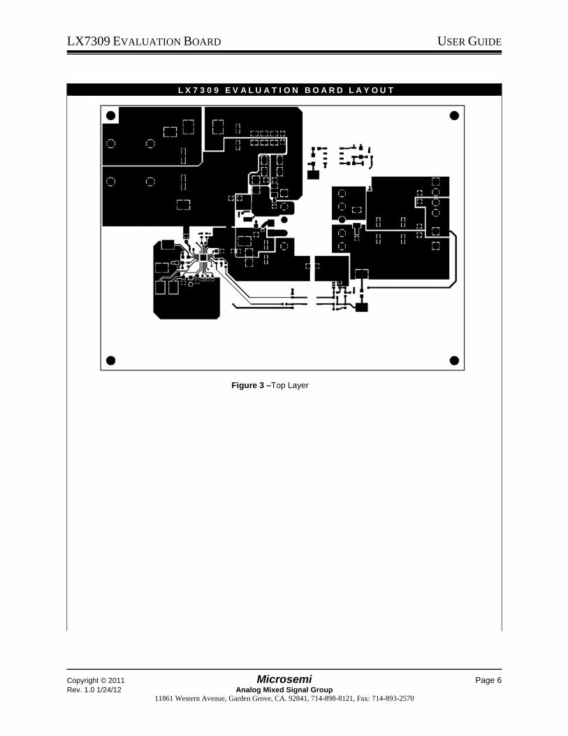
Figure 3 –Top Layer

LX7309 EVALUATION BOARD USER GUIDE
Copyright © 2011 Microsemi Page 7 Rev. 1.0 1/24/12 Analog Mixed Signal Group
11861 Western Avenue, Garden Grove, CA. 92841, 714-898-8121, Fax: 714-893-2570
L X 7 3 0 9 E V A L U A T I O N B O A R D L A Y OU T
Figure 4 –Bottom Layer

LX7309 EVALUATION BOARD USER GUIDE
Copyright © 2012 Microsemi Page 8 Rev. 1.0 1/24/12 Analog Mixed Signal Group
11861 Western Avenue, Garden Grove, CA. 92841, 714-898-8121, Fax: 714-893-2570
TEST CONSIDERATIONS
The following is a guideline for testing the LX7309 IC:
Output ground connections for the evaluation board output (J1 pins 1 and 2) are electrically isolated from the LX7309’s primary ground connections (J6, TP6, and TP11). This should be taken into consideration when grounding test probes.
The evaluation board will quickly become duty cycle limited at input voltages below 37V, and as such it is not recommended to operate below this voltage. It is recommended to operate with VIN UVLO function enabled (J2 installed), which will disable the controller at voltages at or below 36V. The VIN UVLO function is set to disable the controller at VIN falling voltages of 36V or less, and enable the controller at VIN rising voltages of 40V or more. To operate as PFW, remove jumper J2, and monitor signal at TP7. To change the rising and falling voltage thresholds of either the VIN UVLO or PFW functions, change the values of R22, R24, and R26. See the LX7309 Datasheet for further information.
Resistor R27 is a 6.8 Ohm resistor in series with the bootstrap supply providing VCC. This resistor may be used to monitor LX7309’s VCC current (after start-up) with a millivolt DMM.
The PWM frequency can be synchronized to an external clock by connecting a 400kHz signal to TP9 (+) and TP11 (-). The signal should be a 0 to 5V peak signal with a maximum pulse width of 200ns. Care should be taken that the peak signal level input to TP9 does not exceed LX7309’s VDD (pin 18) voltage.
The sync signal should be 2 x the set free-running PWM frequency.
The PWM frequency can be changed by changing resistor R25, however be aware that the transformer and several critical components are designed around 200kHz operation; any gross changes in PWM frequency cannot be tolerated without changing the transformer and other critical components. .
LX7309 EVALUATION BOARD TEST DATA
Note: the above is with post LC filter installed

LX7309 EVALUATION BOARD USER GUIDE
Copyright © 2011 Microsemi Page 9 Rev. 1.0 1/24/12 Analog Mixed Signal Group
11861 Western Avenue, Garden Grove, CA. 92841, 714-898-8121, Fax: 714-893-2570
Full Load Start-up
CH3: VOUT
CH4: Primary Transistor (Q2) Drain

LX7309 EVALUATION BOARD USER GUIDE
Copyright © 2011 Microsemi Page 10 Rev. 1.0 1/24/12 Analog Mixed Signal Group
11861 Western Avenue, Garden Grove, CA. 92841, 714-898-8121, Fax: 714-893-2570
Start-up Delay
CH4: Primary Transistor (Q2) Drain
CH3: VOUT
VCC Start-up
CH3: VCC
CH4: Primary Transistor (Q2) Drain
Power Applied

LX7309 EVALUATION BOARD USER GUIDE
Copyright © 2011 Microsemi Page 11 Rev. 1.0 1/24/12 Analog Mixed Signal Group
11861 Western Avenue, Garden Grove, CA. 92841, 714-898-8121, Fax: 714-893-2570
Full Load Shutdown with VIN UVLO Function
CH1: VIN
CH3: Comp pin (Pin 14)
CH4: Primary Transistor (Q2) Drain
Full Load Shutdown with VIN UVLO Function
CH4: VIN
CH3: VOUT

LX7309 EVALUATION BOARD USER GUIDE
Copyright © 2011 Microsemi Page 12 Rev. 1.0 1/24/12 Analog Mixed Signal Group
11861 Western Avenue, Garden Grove, CA. 92841, 714-898-8121, Fax: 714-893-2570
Full Load Output Ripple
Bode Plot VIN = 48V; 4A Load
LX7309 EVALUATION BOARD USER GUIDE
Copyright © 2011 Microsemi Page 13 Rev. 1.0 1/24/12 Analog Mixed Signal Group
11861 Western Avenue, Garden Grove, CA. 92841, 714-898-8121, Fax: 714-893-2570
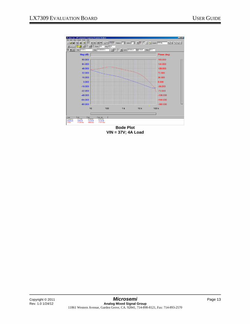
Bode Plot
VIN = 37V; 4A Load

LX7309 EVALUATION BOARD USER GUIDE
Copyright © 2011 Microsemi Page 14 Rev. 1.0 1/24/12 Analog Mixed Signal Group
11861 Western Avenue, Garden Grove, CA. 92841, 714-898-8121, Fax: 714-893-2570
L X 7 3 0 9 E V A L U A T I O N B O A R D S C H E M A T I C
Figure 5 – LX7309 Evaluation Board Schematic

LX7309 EVALUATION BOARD USER GUIDE
Copyright © 2011 Microsemi Page 15 Rev. 1.0 1/24/12 Analog Mixed Signal Group
11861 Western Avenue, Garden Grove, CA. 92841, 714-898-8121, Fax: 714-893-2570
Bill of Materials - LX7309 Evaluation Board
Item Number Quantity Part Reference Description Manufacturer Manufacturer Part Number
1 1 C1 CAP ALU 47uF 100V 20% 12.5mm x 13.5mm Panasonic EEVFK2A470Q 2 3 C2 C3 C4 CAP CER 2.2uF 100V 10% X7R ^1210 SMT CAPAX 1210X225K101SNT 3 1 C5 CAP CRM 100nF 100V 10%^^X7R 1206 SMT EPCOS B37872K1104K62 4 1 C6 CAP CRM 33nF 100V 10%^^X7R 1206 SMT AVX 12061C333KAT2A 5 2 C7 C8 CAP ALUM 180UF 16V 20% 4.36A 16m Ohm 8mm X
12mm SMD United Chemicon APXA160ARA181MHC0G
6 1 C9 CAP CRM 1uF 25V 10% X7R, 1206 TAIYOYUDEN TMK316B7105ML-T 7 1 C10 CAP X7R 10uF 16V 10% 1206 TDK C3216X7R1C106K 8 2 C11 C27 CAP CRM 100nF 25V 10%^^X7R 0805 SMT Murata GRM216R71E104KA01 9 1 C12 Capacitor, 22uF, 25V, Aluminum Electrolytic, 6.3mm x
5.4mm 105C SMD Nichicon
UWT1E220M 10 1 C13 CAP CRM 1nF/2000V 10%++X7R 1206 SMT AVX 1206GC102KAT1A 11 1 C14 Capacitor, X7R, 100nF, 16V, 10% 0603 TAIYOYUDEN GRM216R71E104KA01 12 1 C17 Capacitor, X7R, 220nF, 16V, 10% 0603 TAIYOYUDEN GRM216R71E224KA01 13 1 C15 Capacitor, Ceramic, 1.0uF, 10 Volt, 10%, 0805 Type SMD Panasonic ECJ2YB1A105K 14 1 C16 Capacitor, X7R, 120nF, 16V, 10% 0603 TAIYOYUDEN EMK107B7124KA-T 15 1 C18 CAP CRM 1uF 16V 10%^^X7R 0805 SMT^^ Panasonic ECJ2VB1C105K 16 1 C19 Capacitor, Ceramic, 0.68uF, 16 Volt, 10%, 0805 Type SMD Panasonic ECJ2VB1C684K 17 1 C20 CAP ALU 22uF 100V 20% 8mm X 10mm Panasonic EEEFK2A220P 18 1 C21 CAP CER 1000PF 10V X7R 0603 Kemet C0603C102M8RACTU 19 1 C23 CAP CER 330PF 200V X7R 0805 AVX 08052C331KAT2A 20 1 C24 CAP CER 2700PF 100V X7R 0805 AVX 08051C272KAT2A 21 1 C25 No Stuff 22 1 D1 DIO FAST SWI 150V, 1A Fairchild ES1C 23 1 D2 Diode, Schottky, 200mA, 60V, SOD-323 NXP PMEG6002EJ,115 24 1 D4 IC Adj Prec Shunt Reg 2.5V ^^1% SOT-23-5 SMT Texas
Instruments TL431ACDBVR 25 1 D5 D6 DIO FAST SWI 75V 300mA^^4nS SOD80C MiniMELF Vishay LL4148 26 1 J1 PIN HEADER 4 PIN 0.156"^^TIN, WITH LOCKING WALL CviLux CI5104P1V00 27 1 J2 PIN HEADER 2 PINs^^0.1" PIN SQUER+TIN CviLux CH31-021V100 28 1 J5 90o PCB Mounted Insulated Banana Socket 4mm Red Deltron 571-0500 29 1 J6 90o PCB Mounted Insulated Banana Socket 4mm Black Deltron 571-0100

LX7309 EVALUATION BOARD USER GUIDE
Copyright © 2011 Microsemi Page 16 Rev. 1.0 1/24/12 Analog Mixed Signal Group
11861 Western Avenue, Garden Grove, CA. 92841, 714-898-8121, Fax: 714-893-2570
Bill of Materials - LX7309 Evaluation Board
Item Number Quantity Part Reference Description Manufacturer Manufacturer Part Number
30 1 L1 Inductor, 10uH SMD Inductor, 2.0A, 49m Ohm Wurth 74477710 31 1 L2 Inductor, 1uH SMD Inductor, 5.3A, 11m Ohm Wurth 7447779001 32 1 Q1 FET, N-Channel, 80V, 100A 5.7mΩ Infineon BSC057N08NS3 33 1 Q2 FET, N-Channel, 150V, 9A Fairchild FDMS86200 34 1 Q3 TRN PNP 60V 600mA SOT23 SMT 250mW
MMBT2907AW^ ON Semiconductor MMBT2907AWT1G
35 2 R1 R2 RES 3.3K OHM 1.5W 5% 2512 SMD Vishay CRCW25123K30JNEGHP 36 1 R4 Resistor, 13K Ohms, 1/4 Watt, 5% 1206 Type SMD Panasonic ERJ8GEYJ133V 37 1 R5 Resistor, 6.8 Ohm, 0603 Type SMD Panasonic ERJ3GEY6R80V 38 3 R10 R19 R35 Resistor, 0 Ohm jumper, 0603 Type SMD Panasonic ERJ3GEY0R00V 39 1 R6 Resistor, 20.0 Ohms, 1/8 Watt, 1% 0805 Type SMD Rohm MCR10EZHF20R0 40 3 R7 R23 R28 Resistor, 100K Ohms, 1/8 Watt, 5% 0805 Type SMD Rohm MCR10EZHJ104 41 1 R8 Resistor, 1.1K 1/10 Watt, 5% 0603 Type SMD Panasonic ERJ3GEYJ821V 42 1 R9 RES .043 OHM 1/2W 1% 1206 SMD Panasonic ERJ-8BWFR043V 43 1 R17 Resistor, 1.2K Ohms, 1/10 Watt, 5% 0603 Type SMD Panasonic ERJ3GEYJ122V 44 1 R11 Resistor, 1.5K Ohms, 1/10 Watt, 5% 0603 Type SMD Rohm MCR03EZPJ152 45 1 R26 Resistor, 20.0K Ohms, 1/16 Watt, 1% 0603 Type SMD Panasonic ERJ3EKF2002 46 1 R12 Resistor, 19.1K Ohms, 1/16 Watt, 1% 0603 Type SMD Panasonic ERJ3EKF1912 47 4 R13 R15 R20
R30 No Stuff
48 2 R14 R16 Resistor,20.0K Ohms, 1/16 Watt, 1% 0603 Type SMD Panasonic ERJ3EKF2002 49 1 R18 Resistor, 4.99K Ohms, 1/16 Watt, 1% 0603 Type SMD Panasonic ERJ3EKF4991 50 2 R31, R32 Resistor, 100 Ohms, 1/10 Watt, 5% 0603 Type SMD Panasonic ERJ3GSYJ101 51 1 R21 Resistor, 1K Ohms, 1/4 Watt, 5% 1206 Type SMD Panasonic ERJ8GEYJ102V 52 1 R22 Resistor, 634K Ohms, 1/8 Watt, 1% 0805 Type SMD Panasonic ERJ6ENF6343 53 1 R24 Resistor, 750K Ohms, 1/16 Watt, 1% 0603 Type SMD Panasonic ERJ3EKF7503 54 1 R25 Resistor, 49.9K Ohms, 1/16 Watt, 1% 0603 Type SMD Panasonic ERJ3EKF4992 55 1 R29 Resistor, 24 Ohms, 1/4 Watt, 5% 1206 Type SMD Panasonic ERJ8GEYJ240V 56 1 R33 Resistor, 43 Ohms 1/2 Watt 5% 1210 Type SMD Panasonic ERJ-14YJ430U 57 1 R34 Resistor, 5.1 Ohms 1W 5% 2512 Type SMD Panasonic ERJ-1TYJ5R1U 58 1 T1 48W transformer; TMP SGE2944-1 59 1 T2 Transformer, Gate Drive, 1:1 turns ratio, Coilcraft FA2659-AL

LX7309 EVALUATION BOARD USER GUIDE
Copyright © 2011 Microsemi Page 17 Rev. 1.0 1/24/12 Analog Mixed Signal Group
11861 Western Avenue, Garden Grove, CA. 92841, 714-898-8121, Fax: 714-893-2570
Bill of Materials - LX7309 Evaluation Board
Item Number Quantity Part Reference Description Manufacturer Manufacturer Part Number
60 10 TP1 TP2 TP3 TP5 TP6 TP7 TP8 TP9 TP10 TP11
Terminal, Compact style test point, SMT PCB Mount Keystone 5016
61 1 TP4 Terminal, Miniature style test point, SMT PCB Mount Keystone 5015 62 1 U1 IC, POE PD PWM Controller, 24 pin 4mm x 4mm QFN Microsemi LX7309 63 1 U2 Optoisolator, CTR = 100 to 200, SMT mount NEC P2711-1-M-A 64 1 VR1 Diode, Zener, 15V, 100mW, SOD-523 Micro
Commercial Co.
BZT52C15T
65 1 PCB Printed Circuit Board Microsemi SGE3256 X2