ltc6992-1/ltc6992-2/ ltc6992-3/ltc6992-4 - … 0v to 1v analog input n four available options define...
TRANSCRIPT
LTC6992-1/LTC6992-2/LTC6992-3/LTC6992-4
169921234fc
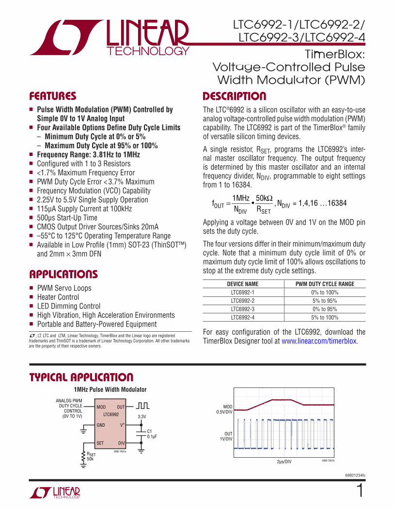
Typical applicaTion
DescripTion
TimerBlox: Voltage-Controlled Pulse Width Modulator (PWM)
The LTC®6992 is a silicon oscillator with an easy-to-use analog voltage-controlled pulse width modulation (PWM) capability. The LTC6992 is part of the TimerBlox® family of versatile silicon timing devices.
A single resistor, RSET, programs the LTC6992’s inter-nal master oscillator frequency. The output frequency is determined by this master oscillator and an internal frequency divider, NDIV, programmable to eight settings from 1 to 16384.
fOUT = 1MHz
NDIV•
50kΩRSET
,NDIV = 1,4,16 …16384
Applying a voltage between 0V and 1V on the MOD pin sets the duty cycle.
The four versions differ in their minimum/maximum duty cycle. Note that a minimum duty cycle limit of 0% or maximum duty cycle limit of 100% allows oscillations to stop at the extreme duty cycle settings.
DEVICE NAME PWM DUTY CYCLE RANGELTC6992-1 0% to 100%LTC6992-2 5% to 95%LTC6992-3 0% to 95%LTC6992-4 5% to 100%
For easy configuration of the LTC6992, download the TimerBlox Designer tool at www.linear.com/timerblox.
n Pulse Width Modulation (PWM) Controlled by Simple 0V to 1V Analog Input
n Four Available Options Define Duty Cycle Limits – Minimum Duty Cycle at 0% or 5% – Maximum Duty Cycle at 95% or 100%n Frequency Range: 3.81Hz to 1MHzn Configured with 1 to 3 Resistorsn <1.7% Maximum Frequency Errorn PWM Duty Cycle Error < 3.7% Maximumn Frequency Modulation (VCO) Capabilityn 2.25V to 5.5V Single Supply Operationn 115μA Supply Current at 100kHzn 500μs Start-Up Timen CMOS Output Driver Sources/Sinks 20mAn –55°C to 125°C Operating Temperature Rangen Available in Low Profile (1mm) SOT-23 (ThinSOT™)
and 2mm × 3mm DFN
L, LT, LTC and LTM, Linear Technology, TimerBlox and the Linear logo are registered trademarks and ThinSOT is a trademark of Linear Technology Corporation. All other trademarks are the property of their respective owners.
FeaTures
applicaTionsn PWM Servo Loopsn Heater Controln LED Dimming Controln High Vibration, High Acceleration Environmentsn Portable and Battery-Powered Equipment
6992 TA01a
LTC6992
MOD
GND
SET
OUT
V+
DIV
RSET50k
3.3V
ANALOG PWMDUTY CYCLE
CONTROL(0V TO 1V)
C10.1µF
1MHz Pulse Width Modulator
MOD0.5V/DIV
OUT1V/DIV
2µs/DIV 6992 TA01b

LTC6992-1/LTC6992-2/LTC6992-3/LTC6992-4
269921234fc
absoluTe MaxiMuM raTingsSupply Voltage (V+) to GND .........…………………….6VMaximum Voltage On Any Pin
............................. (GND – 0.3V) ≤ VPIN ≤ (V+ + 0.3V)Operating Temperature Range (Note 2)
LTC6992C ............................................–40°C to 85°C LTC6992I .............................................–40°C to 85°C LTC6992H .......................................... –40°C to 125°C LTC6992MP ....................................... –55°C to 125°C
(Note 1)
TOP VIEW
OUT
GND
MOD
V+
DIV
SET
DCB PACKAGE6-LEAD (2mm × 3mm) PLASTIC DFN
4
57GND
6
3
2
1
TJMAX = 150°C, θJA = 64°C/W, θJC = 10.6°C/W
EXPOSED PAD (PIN 7) IS GND, PCB CONNECTION IS OPTIONAL
MOD 1
GND 2
SET 3
6 OUT
5 V+
4 DIV
TOP VIEW
S6 PACKAGE6-LEAD PLASTIC TSOT-23
TJMAX = 150°C, θJA = 192°C/W, θJC = 51°C/W
pin conFiguraTion
orDer inForMaTion
Specified Temperature Range (Note 3) LTC6992C ................................................ 0°C to 70°C LTC6992I .............................................–40°C to 85°C LTC6992H .......................................... –40°C to 125°C LTC6992MP ....................................... –55°C to 125°C
Junction Temperature .......................................... 150°CStorage Temperature Range .................. –65°C to 150°CLead Temperature (Soldering, 10 sec)
S6 Package ....................................................... 300°C
Lead Free FinishTAPE AND REEL (MINI) TAPE AND REEL PART MARKING* PACKAGE DESCRIPTION SPECIFIED TEMPERATURE RANGELTC6992CDCB-1#TRMPBF LTC6992CDCB-1#TRPBF LDXC 6-Lead (2mm × 3mm) Plastic DFN 0°C to 70°CLTC6992IDCB-1#TRMPBF LTC6992IDCB-1#TRPBF LDXC 6-Lead (2mm × 3mm) Plastic DFN –40°C to 85°CLTC6992HDCB-1#TRMPBF LTC6992HDCB-1#TRPBF LDXC 6-Lead (2mm × 3mm) Plastic DFN –40°C to 125°CLTC6992CS6-1#TRMPBF LTC6992CS6-1#TRPBF LTDXB 6-Lead Plastic TSOT-23 0°C to 70°CLTC6992IS6-1#TRMPBF LTC6992IS6-1#TRPBF LTDXB 6-Lead Plastic TSOT-23 –40°C to 85°CLTC6992HS6-1#TRMPBF LTC6992HS6-1#TRPBF LTDXB 6-Lead Plastic TSOT-23 –40°C to 125°CLTC6992CDCB-2#TRMPBF LTC6992CDCB-2#TRPBF LDXF 6-Lead (2mm × 3mm) Plastic DFN 0°C to 70°CLTC6992IDCB-2#TRMPBF LTC6992IDCB-2#TRPBF LDXF 6-Lead (2mm × 3mm) Plastic DFN –40°C to 85°CLTC6992HDCB-2#TRMPBF LTC6992HDCB-2#TRPBF LDXF 6-Lead (2mm × 3mm) Plastic DFN –40°C to 125°CLTC6992CS6-2#TRMPBF LTC6992CS6-2#TRPBF LTDXD 6-Lead Plastic TSOT-23 0°C to 70°CLTC6992IS6-2#TRMPBF LTC6992IS6-2#TRPBF LTDXD 6-Lead Plastic TSOT-23 –40°C to 85°CLTC6992HS6-2#TRMPBF LTC6992HS6-2#TRPBF LTDXD 6-Lead Plastic TSOT-23 –40°C to 125°CLTC6992CDCB-3#TRMPBF LTC6992CDCB-3#TRPBF LFCP 6-Lead (2mm × 3mm) Plastic DFN 0°C to 70°CLTC6992IDCB-3#TRMPBF LTC6992IDCB-3#TRPBF LFCP 6-Lead (2mm × 3mm) Plastic DFN –40°C to 85°CLTC6992HDCB-3#TRMPBF LTC6992HDCB-3#TRPBF LFCP 6-Lead (2mm × 3mm) Plastic DFN –40°C to 125°CLTC6992CS6-3#TRMPBF LTC6992CS6-3#TRPBF LTFCQ 6-Lead Plastic TSOT-23 0°C to 70°CLTC6992IS6-3#TRMPBF LTC6992IS6-3#TRPBF LTFCQ 6-Lead Plastic TSOT-23 –40°C to 85°CLTC6992HS6-3#TRMPBF LTC6992HS6-3#TRPBF LTFCQ 6-Lead Plastic TSOT-23 –40°C to 125°C
LTC6992-1/LTC6992-2/LTC6992-3/LTC6992-4
369921234fc
orDer inForMaTion
The l denotes the specifications which apply over the full operating temperature range, otherwise specifications are at TA = 25°C. Test conditions are V+ = 2.25V to 5.5V, VMOD = 0V to VSET,DIVCODE = 0 to 15 (NDIV = 1 to 16,384), RSET = 50k to 800k, RLOAD = 5k, CLOAD = 5pF unless otherwise noted.
elecTrical characTerisTics
SYMBOL PARAMETER CONDITIONS MIN TYP MAX UNITS
Oscillation Frequency
fOUT Output Frequency 3.81 1000000 Hz
∆fOUT Frequency Accuracy (Note 4) 3.81Hz ≤ fOUT ≤ 1MHz l
±0.8 ±1.7 ±2.4
% %
∆fOUT/∆T Frequency Drift Over Temperature l ±0.005 %/°C
∆fOUT/∆V+ Frequency Drift Over Supply V+ = 4.5V to 5.5V V+ = 2.25V to 4.5V
l
l
0.25 0.08
0.65 0.18
%/V %/V
Long-Term Frequency Stability (Note 10) 90 ppm/√kHr
Period Jitter (Note 9) NDIV = 1 1.2 %P-P
NDIV = 4 0.4 0.07
%P-P %RMS
NDIV = 16 0.15 0.022
%P-P %RMS
Pulse Width Modulation
∆D PWM Duty Cycle Accuracy VMOD = 0.2 • VSET to 0.8 • VSET VMOD = 0.2 • VSET to 0.8 • VSET VMOD < 0.2 • VSET or VMOD > 0.8 • VSET
l
l
±3.0 ±3.7 ±4.5 ±4.9
% % %
DMAX Maximum Duty Cycle Limit LTC6992-1/LTC6992-4, POL = 0, VMOD = 1V l 100 %
LTC6992-2/LTC6992-3, POL = 0, VMOD = 1V l 90.5 95 99 %
DMIN Minimum Duty Cycle Limit LTC6992-1/LTC6992-3, POL = 0, VMOD = 0V l 0 %
LTC6992-2/LTC6992-4, POL = 0, VMOD = 0V l 1 5 9.5 %
tS,PWM Duty Cycle Settling Time (Note 6) tMASTER = tOUT/NDIV 8•tMASTER µs
Lead Free FinishTAPE AND REEL (MINI) TAPE AND REEL PART MARKING* PACKAGE DESCRIPTION SPECIFIED TEMPERATURE RANGELTC6992CDCB-4#TRMPBF LTC6992CDCB-4#TRPBF LFCR 6-Lead (2mm × 3mm) Plastic DFN 0°C to 70°CLTC6992IDCB-4#TRMPBF LTC6992IDCB-4#TRPBF LFCR 6-Lead (2mm × 3mm) Plastic DFN –40°C to 85°CLTC6992HDCB-4#TRMPBF LTC6992HDCB-4#TRPBF LFCR 6-Lead (2mm × 3mm) Plastic DFN –40°C to 125°CLTC6992CS6-4#TRMPBF LTC6992CS6-4#TRPBF LTFCS 6-Lead Plastic TSOT-23 0°C to 70°CLTC6992IS6-4#TRMPBF LTC6992IS6-4#TRPBF LTFCS 6-Lead Plastic TSOT-23 –40°C to 85°CLTC6992HS6-4#TRMPBF LTC6992HS6-4#TRPBF LTFCS 6-Lead Plastic TSOT-23 –40°C to 125°CLTC6992MPS6-1#TRMPBF LTC6992MPS6-1#TRPBF LTDXB 6-Lead Plastic TSOT-23 –55°C to 125°CLTC6992MPS6-2#TRMPBF LTC6992MPS6-2#TRPBF LTDXD 6-Lead Plastic TSOT-23 –55°C to 125°CLTC6992MPS6-3#TRMPBF LTC6992MPS6-3#TRPBF LTFCQ 6-Lead Plastic TSOT-23 –55°C to 125°CLTC6992MPS6-4#TRMPBF LTC6992MPS6-4#TRPBF LTFCS 6-Lead Plastic TSOT-23 –55°C to 125°CTRM = 500 pieces. *Temperature grades are identified by a label on the shipping container.Consult LTC Marketing for parts specified with wider operating temperature ranges. Consult LTC Marketing for information on lead based finish parts.For more information on lead free part marking, go to: http://www.linear.com/leadfree/ For more information on tape and reel specifications, go to: http://www.linear.com/tapeandreel/
LTC6992-1/LTC6992-2/LTC6992-3/LTC6992-4
469921234fc
The l denotes the specifications which apply over the full operating temperature range, otherwise specifications are at TA = 25°C. Test conditions are V+ = 2.25V to 5.5V, VMOD = 0V to VSET,DIVCODE = 0 to 15 (NDIV = 1 to 16,384), RSET = 50k to 800k, RLOAD = 5k, CLOAD = 5pF unless otherwise noted.
elecTrical characTerisTics
SYMBOL PARAMETER CONDITIONS MIN TYP MAX UNITS
Power Supply
V+ Operating Supply Voltage Range l 2.25 5.5 V
Power-On Reset Voltage l 1.95 V
IS Supply Current RL = ∞, RSET = 50k, NDIV = 1
V+ = 5.5V l 365 450 µA
V+ = 2.25V l 225 285 µA
RL = ∞, RSET = 50k, NDIV = 4
V+ = 5.5V l 350 420 µA
V+ = 2.25V l 225 280 µA
RL = ∞, RSET = 50k, NDIV ≥ 16
V+ = 5.5V l 325 390 µA
V+ = 2.25V l 215 265 µA
RL = ∞, RSET = 800k, NDIV = 1 to 16,384
V+ = 5.5V l 120 170 µA
V+ = 2.25V l 105 150 µA
Analog Inputs
VSET Voltage at SET Pin l 0.97 1.00 1.03 V
∆VSET/∆T VSET Drift Over Temperature l ±75 µV/°C
RSET Frequency-Setting Resistor l 50 800 kΩ
MOD Pin Input Capacitance 2.5 pF
MOD Pin Input Current l ±10 nA
VMOD,HI VMOD Voltage for Maximum Duty Cycle
LTC6992-1/LTC6992-4, POL = 0, D = 100% LTC6992-2/LTC6992-3, POL = 0, D = 95%
l 0.90•VSET 0.86•VSET
0.936•VSET V V
VMOD,LO VMOD Voltage for Minimum Duty Cycle
LTC6992-1/LTC6992-3, POL = 0, D = 0% LTC6992-2/LTC6992-4, POL = 0, D = 5%
l 0.064•VSET 0.10•VSET 0.14•VSET
V V
VDIV DIV Pin Voltage l 0 V+ V
∆VDIV/∆V+ DIV Pin Valid Code Range (Note 5) Deviation from Ideal VDIV/V+ = (DIVCODE + 0.5)/16
l ±1.5 %
DIV Pin Input Current l ±10nA
Digital Output
IOUT(MAX) Output Current V+ = 2.7V to 5.5V ±20 mA
VOH High Level Output Voltage (Note 7) V+ = 5.5V IOUT = –1mA IOUT = –16mA
l
l
5.45 4.84
5.48 5.15
V V
V+ = 3.3V IOUT = –1mA IOUT = –10mA
l
l
3.24 2.75
3.27 2.99
V V
V+ = 2.25V IOUT = –1mA IOUT = -8mA
l
l
2.17 1.58
2.21 1.88
V V
VOL Low Level Output Voltage (Note 7) V+ = 5.5V IOUT = 1mA IOUT = 16mA
l
l
0.02 0.26
0.04 0.54
V V
V+ = 3.3V IOUT = 1mA IOUT = 10mA
l
l
0.03 0.22
0.05 0.46
V V
V+ = 2.25V IOUT = 1mA IOUT = 8mA
l
l
0.03 0.26
0.07 0.54
V V
tr Output Rise Time (Note 8) V+ = 5.5V, RLOAD = ∞ V+ = 3.3V, RLOAD = ∞ V+ = 2.25V, RLOAD = ∞
1.1 1.7 2.7
ns ns ns
tf Output Fall Time (Note 8) V+ = 5.5V, RLOAD = ∞ V+ = 3.3V, RLOAD = ∞ V+ = 2.25V, RLOAD = ∞
1.0 1.6 2.4
ns ns ns

LTC6992-1/LTC6992-2/LTC6992-3/LTC6992-4
569921234fc
Note 1: Stresses beyond those listed under Absolute Maximum Ratings may cause permanent damage to the device. Exposure to any Absolute Maximum Rating condition for extended periods may affect device reliability and lifetime.Note 2: The LTC6992C is guaranteed functional over the operating temperature range of –40°C to 85°C.Note 3: The LTC6992C is guaranteed to meet specified performance from 0°C to 70°C. The LTC6992C is designed, characterized and expected to meet specified performance from –40°C to 85°C but it is not tested or QA sampled at these temperatures. The LTC6992I is guaranteed to meet specified performance from –40°C to 85°C. The LTC6992H is guaranteed to meet specified performance from –40°C to 125°C. The LTC6992MP is guaranteed to meet specified performance from –55°C to 125°C.Note 4: Frequency accuracy is defined as the deviation from the fOUT equation, assuming RSET is used to program the frequency.Note 5: See Operation section, Table 1 and Figure 2 for a full explanation of how the DIV pin voltage selects the value of DIVCODE.Note 6: Duty cycle settling time is the amount of time required for the output to settle within ±1% of the final duty cycle after a ±10% change in the setting (±80mV step in VMOD).
Note 7: To conform to the Logic IC Standard, current out of a pin is arbitrarily given a negative value.Note 8: Output rise and fall times are measured between the 10% and the 90% power supply levels with 5pF output load. These specifications are based on characterization.Note 9: Jitter is the ratio of the peak-to-peak deviation of the period to the mean of the period. This specification is based on characterization and is not 100% tested.Note 10: Long-term drift of silicon oscillators is primarily due to the movement of ions and impurities within the silicon and is tested at 30°C under otherwise nominal operating conditions. Long-term drift is specified as ppm/√kHr due to the typically nonlinear nature of the drift. To calculate drift for a set time period, translate that time into thousands of hours, take the square root and multiply by the typical drift number. For instance, a year is 8.77kHr and would yield a drift of 266ppm at 90ppm/√kHr. Drift without power applied to the device may be approximated as 1/10th of the drift with power, or 9ppm/√kHr for a 90ppm/√kHr device.
elecTrical characTerisTics
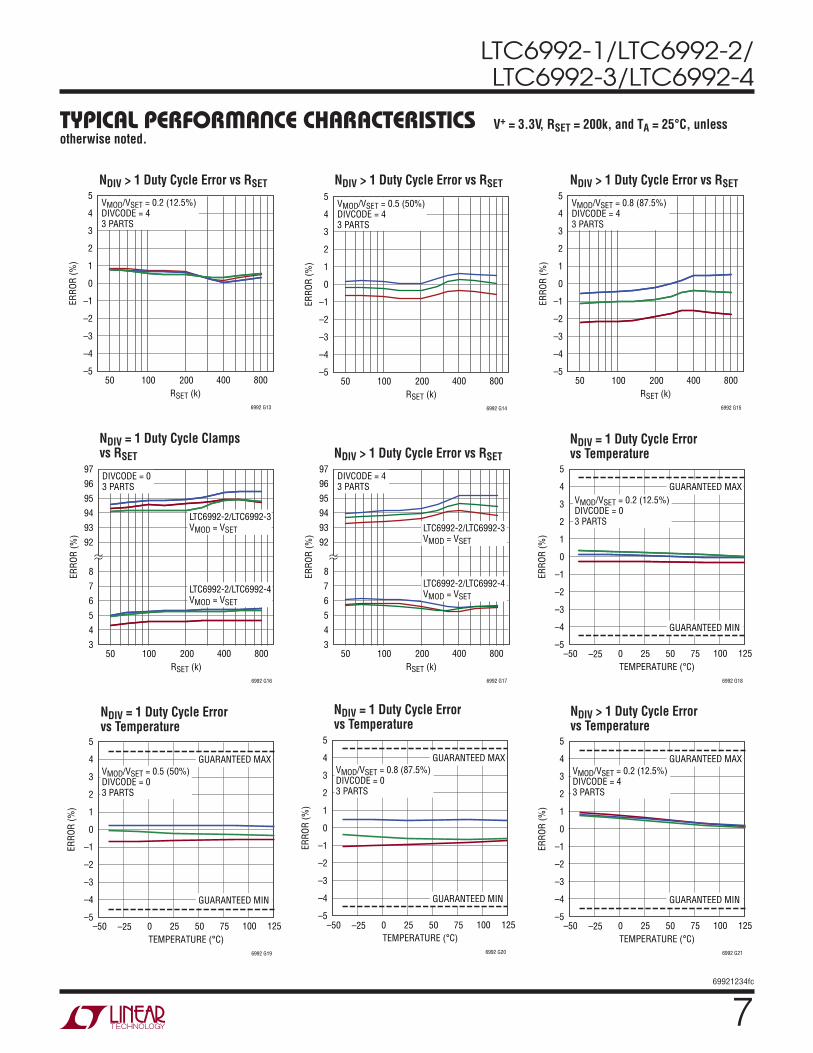
Typical perForMance characTerisTics
Frequency Error vs Temperature Frequency Error vs Temperature Frequency Error vs Temperature
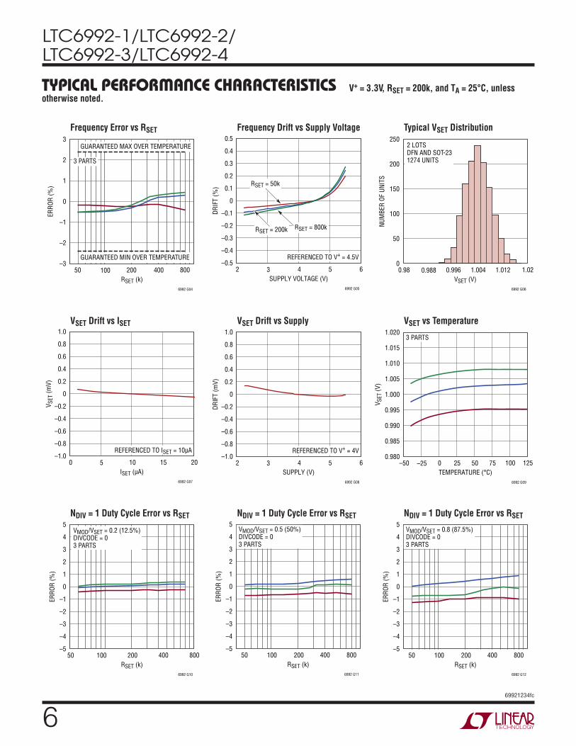
V+ = 3.3V, RSET = 200k, and TA = 25°C, unless otherwise noted.
TEMPERATURE (°C)–50
–3
0
1
2
3
0 25 50 100 125
–1
–2
–25 75
6992 G01
ERRO
R (%
)
RSET = 50k3 PARTS
GUARANTEED MAX OVER TEMPERATURE
GUARANTEED MIN OVER TEMPERATURE
TEMPERATURE (°C)–50
–3
0
1
2
3
0 25 50 100 125
–1
–2
–25 75
6992 G02
ERRO
R (%
)
RSET = 200k3 PARTS
GUARANTEED MAX OVER TEMPERATURE
GUARANTEED MIN OVER TEMPERATURE
TEMPERATURE (°C)–50
–3
0
1
2
3
0 25 50 100 125
–1
–2
–25 75
6992 G03
ERRO
R (%
)
RSET = 800k3 PARTS
GUARANTEED MAX OVER TEMPERATURE
GUARANTEED MIN OVER TEMPERATURE
LTC6992-1/LTC6992-2/LTC6992-3/LTC6992-4
669921234fc
Frequency Error vs RSET Frequency Drift vs Supply Voltage Typical VSET Distribution
VSET Drift vs ISET VSET Drift vs Supply VSET vs Temperature
RSET (k)50
–3
0
1
2
3
200 400 800
–1
–2
100
6992 G04
ERRO
R (%
)
3 PARTS
GUARANTEED MAX OVER TEMPERATURE
GUARANTEED MIN OVER TEMPERATURE
SUPPLY VOLTAGE (V)2
–0.5
0
0.2
0.1
0.3
0.4
0.5
4 5 6
–0.2
–0.1
–0.3
–0.4
3
6992 G05
DRIF
T (%
)
REFERENCED TO V+ = 4.5V
RSET = 50k
RSET = 200k RSET = 800k
VSET (V)0.98
0
100
50
150
200
250
0.996 1.004 1.012 1.020.988
6992 G06
NUM
BER
OF U
NITS
2 LOTSDFN AND SOT-231274 UNITS
ISET (µA)0
–1.0
0
0.4
0.2
0.6
0.8
1.0
10 15 20
–0.4
–0.2
–0.6
–0.8
5
6992 G07
V SET
(mV)
REFERENCED TO ISET = 10µA
SUPPLY (V)2
–1.0
0
0.4
0.2
0.6
0.8
1.0
4 5 6
–0.4
–0.2
–0.6
–0.8
3
6992 G08
DRIF
T (m
V)
REFERENCED TO V+ = 4V
TEMPERATURE (°C)–50
0.980
1.000
1.010
1.005
1.015
1.020
0 25 50 100 125
0.995
0.990
0.985
–25 75
6992 G09
V SET
(V)
3 PARTS
NDIV = 1 Duty Cycle Error vs RSET NDIV = 1 Duty Cycle Error vs RSET NDIV = 1 Duty Cycle Error vs RSET
RSET (k)50
–5
0
3
2
1
4
5
100 400 800
–1
–2
–3
–4
200
6992 G10
ERRO
R (%
)
VMOD/VSET = 0.2 (12.5%)DIVCODE = 03 PARTS
RSET (k)50
–5
0
3
2
1
4
5
100 400 800
–1
–2
–3
–4
200
6992 G11
ERRO
R (%
)
VMOD/VSET = 0.5 (50%)DIVCODE = 03 PARTS
RSET (k)50
–5
0
3
2
1
4
5
100 400 800
–1
–2
–3
–4
200
6992 G12
ERRO
R (%
)
VMOD/VSET = 0.8 (87.5%)DIVCODE = 03 PARTS
Typical perForMance characTerisTics V+ = 3.3V, RSET = 200k, and TA = 25°C, unless otherwise noted.
LTC6992-1/LTC6992-2/LTC6992-3/LTC6992-4
769921234fc
Typical perForMance characTerisTics
NDIV > 1 Duty Cycle Error vs RSET NDIV > 1 Duty Cycle Error vs RSET NDIV > 1 Duty Cycle Error vs RSET
NDIV = 1 Duty Cycle Clamps vs RSET NDIV > 1 Duty Cycle Error vs RSET
RSET (k)50
–5
0
3
2
1
4
5
100 400 800
–1
–2
–3
–4
200
6992 G13
ERRO
R (%
)
VMOD/VSET = 0.2 (12.5%)DIVCODE = 43 PARTS
RSET (k)50
–5
0
3
2
1
4
5
100 400 800
–1
–2
–3
–4
200
6992 G14
ERRO
R (%
)
VMOD/VSET = 0.5 (50%)DIVCODE = 43 PARTS
RSET (k)50
–5
0
3
2
1
4
5
100 400 800
–1
–2
–3
–4
200
6992 G15
ERRO
R (%
)
VMOD/VSET = 0.8 (87.5%)DIVCODE = 43 PARTS
RSET (k)50
3
8
95
94
93
92
96
97
100 400 800
7
6
5
4
200
6992 G16
ERRO
R (%
)
DIVCODE = 03 PARTS
LTC6992-2/LTC6992-3VMOD = VSET
LTC6992-2/LTC6992-4VMOD = VSET
RSET (k)50
3
8
95
94
93
92
96
97
100 400 800
7
6
5
4
200
6992 G17
ERRO
R (%
)
DIVCODE = 43 PARTS
LTC6992-2/LTC6992-3VMOD = VSET
LTC6992-2/LTC6992-4VMOD = VSET
V+ = 3.3V, RSET = 200k, and TA = 25°C, unless otherwise noted.
NDIV = 1 Duty Cycle Error vs Temperature
TEMPERATURE (°C)–50
–5
0
1
2
3
4
5
0 25 50 100 125
–1
–2
–3
–4
–25 75
6992 G18
ERRO
R (%
)
VMOD/VSET = 0.2 (12.5%)DIVCODE = 03 PARTS
GUARANTEED MAX
GUARANTEED MIN
NDIV = 1 Duty Cycle Error vs Temperature
TEMPERATURE (°C)–50
–5
0
1
2
3
4
5
0 25 50 100 125
–1
–2
–3
–4
–25 75
6992 G19
ERRO
R (%
)
VMOD/VSET = 0.5 (50%)DIVCODE = 03 PARTS
GUARANTEED MAX
GUARANTEED MIN
NDIV = 1 Duty Cycle Error vs Temperature
TEMPERATURE (°C)
–5
0
1
2
3
4
5
–1
–2
–3
–4
6992 G20
ERRO
R (%
)
VMOD/VSET = 0.8 (87.5%)DIVCODE = 03 PARTS
GUARANTEED MAX
GUARANTEED MIN
–50 0 25 50 100 125–25 75
NDIV > 1 Duty Cycle Error vs Temperature
TEMPERATURE (°C)–50
–5
0
1
2
3
4
5
0 25 50 100 125
–1
–2
–3
–4
–25 75
6992 G21
ERRO
R (%
)
VMOD/VSET = 0.2 (12.5%)DIVCODE = 43 PARTS
GUARANTEED MAX
GUARANTEED MIN

LTC6992-1/LTC6992-2/LTC6992-3/LTC6992-4
869921234fc
Typical perForMance characTerisTics
NDIV > 1 Duty Cycle Error vs Temperature
NDIV > 1 Duty Cycle Error vs Temperature
NDIV = 1 Duty Cycle Clamps vs Temperature
NDIV > 1 Duty Cycle Clamps vs Temperature
TEMPERATURE (°C)–50
–5
0
1
2
3
4
5
0 25 50 100 125
–1
–2
–3
–4
–25 75
6992 G22
ERRO
R (%
)
VMOD/VSET = 0.5 (50%)DIVCODE = 43 PARTS
GUARANTEED MAX
GUARANTEED MIN
TEMPERATURE (°C)–50
–5
0
1
2
3
4
5
0 25 50 100 125
–1
–2
–3
–4
–25 75
6992 G23
ERRO
R (%
)
VMOD/VSET = 0.8 (87.5%)DIVCODE = 43 PARTS
GUARANTEED MAX
GUARANTEED MIN
TEMPERATURE (°C)–50 –25
3
8
95
94
93
92
96
97
50250 100 125
7
6
5
4
75
6992 G24
ERRO
R (%
)
DIVCODE = 03 PARTS
LTC6992-2/LTC6992-3VMOD = VSET
LTC6992-2/LTC6992-4VMOD = GND
TEMPERATURE (°C)–50 –25
3
8
95
94
93
92
96
97
50250 100 125
7
6
5
4
75
6992 G25
DUTY
CYC
LE (%
)
DIVCODE = 43 PARTS
LTC6992-2/LTC6992-3VMOD = VSET
LTC6992-2/LTC6992-4VMOD = GND
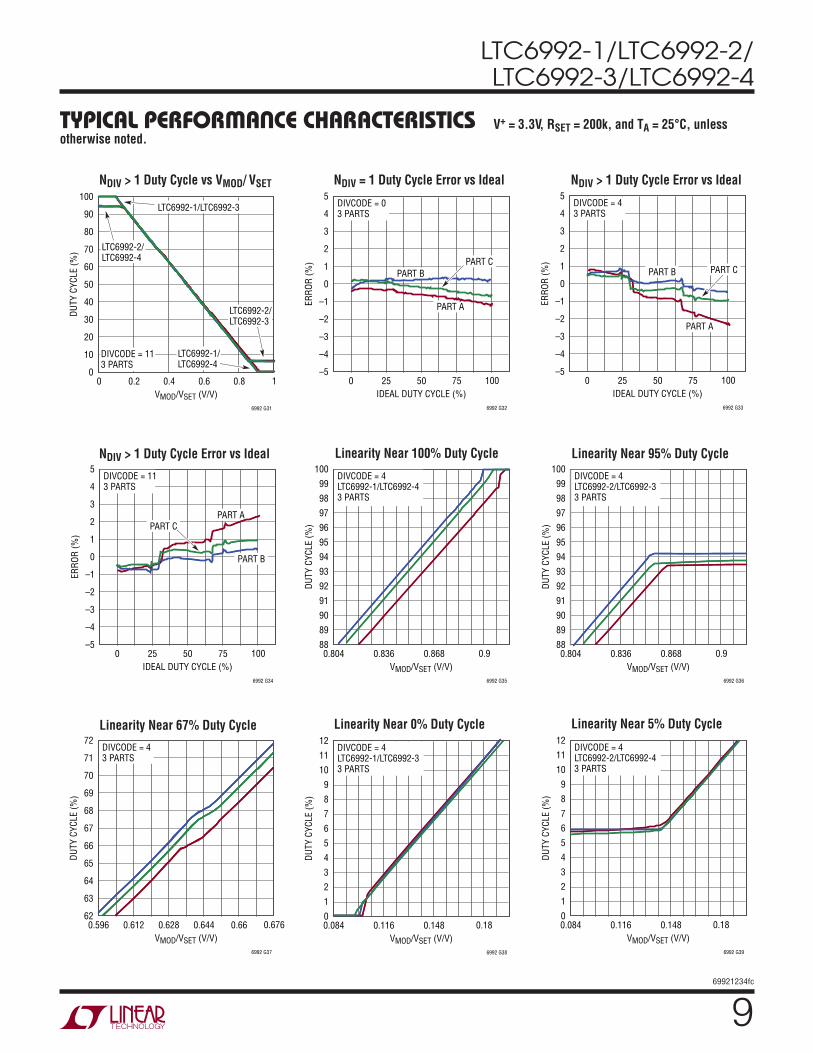
V+ = 3.3V, RSET = 200k, and TA = 25°C, unless otherwise noted.
NDIV = 1 Duty Cycle vs VMOD/ VSET NDIV > 1 Duty Cycle vs VMOD/ VSET
Duty Cycle Error vs DIVCODE Duty Cycle Error vs DIVCODE
Duty Cycle Error vs DIVCODE
VMOD/VSET (V/V)0 0.2
0
40
80
70
60
50
90
100
0.80.60.4 1
30
20
10
6992 G29
DUTY
CYC
LE (%
)
DIVCODE = 03 PARTS LTC6992-1/
LTC6992-4
LTC6992-2/LTC6992-4
LTC6992-1/LTC6992-3
LTC6992-2/LTC6992-3
VMOD/VSET (V/V)0 0.2
0
40
80
70
60
50
90
100
0.80.60.4 1
30
20
10
6992 G30
DUTY
CYC
LE (%
)
DIVCODE = 43 PARTS LTC6992-1/
LTC6992-4
LTC6992-2/LTC6992-4
LTC6992-1/LTC6992-3
LTC6992-2/LTC6992-3
DIVCODE0 2
–5
–1
3
2
1
0
4
5
864 12 14
–2
–3
–4
10
6992 G26
ERRO
R (%
)
VMOD/VSET = 0.2 (12.5%)3 PARTS
DIVCODE0 2
–5
–1
3
2
1
0
4
5
864 12 14
–2
–3
–4
10
6992 G27
ERRO
R (%
)
VMOD/VSET = 0.5 (50%)3 PARTS
DIVCODE0 2
–5
–1
3
2
1
0
4
5
864 12 14
–2
–3
–4
10
6992 G28
ERRO
R (%
)
VMOD/VSET = 0.8 (87.5%)3 PARTS
LTC6992-1/LTC6992-2/LTC6992-3/LTC6992-4
969921234fc
Typical perForMance characTerisTics
NDIV > 1 Duty Cycle vs VMOD/ VSET NDIV = 1 Duty Cycle Error vs Ideal NDIV > 1 Duty Cycle Error vs Ideal
NDIV > 1 Duty Cycle Error vs Ideal
VMOD/VSET (V/V)0 0.2
0
40
80
70
60
50
90
100
0.80.60.4 1
30
20
10
6992 G31
DUTY
CYC
LE (%
)
DIVCODE = 113 PARTS
LTC6992-1/LTC6992-4
LTC6992-2/LTC6992-4
LTC6992-1/LTC6992-3
LTC6992-2/LTC6992-3
IDEAL DUTY CYCLE (%)
–5
0
4
3
2
1
5
50250 100
–1
–2
–3
–4
75
6992 G32
ERRO
R (%
)
DIVCODE = 03 PARTS
PART A
PART BPART C
IDEAL DUTY CYCLE (%)
–5
0
4
3
2
1
5
50250 100
–1
–2
–3
–4
75
6992 G33
ERRO
R (%
)
DIVCODE = 43 PARTS
PART A
PART B PART C
IDEAL DUTY CYCLE (%)
–5
0
4
3
2
1
5
50250 100
–1
–2
–3
–4
75
6992 G34
ERRO
R (%
)
DIVCODE = 113 PARTS
PART A
PART B
PART C
V+ = 3.3V, RSET = 200k, and TA = 25°C, unless otherwise noted.
Linearity Near 100% Duty Cycle
VMOD/VSET (V/V)
88
95
99
98
97
96
100
0.8360.804 0.9
94
93
92
91
90
89
0.868
6992 G35
DUTY
CYC
LE (%
)
DIVCODE = 4LTC6992-1/LTC6992-43 PARTS
Linearity Near 95% Duty Cycle
VMOD/VSET (V/V)
88
95
99
98
97
96
100
0.8360.804 0.9
94
93
92
91
90
89
0.868
6992 G36
DUTY
CYC
LE (%
)
DIVCODE = 4LTC6992-2/LTC6992-33 PARTS
Linearity Near 67% Duty Cycle
VMOD/VSET (V/V)
62
67
71
70
69
68
72
0.612 0.628 0.6440.596 0.676
66
65
64
63
0.66
6992 G37
DUTY
CYC
LE (%
)
DIVCODE = 43 PARTS
Linearity Near 0% Duty Cycle
VMOD/VSET (V/V)
0
7
11
10
9
8
12
0.116 0.1480.084 0.18
6
5
4
3
2
1
6992 G38
DUTY
CYC
LE (%
)
DIVCODE = 4LTC6992-1/LTC6992-33 PARTS
Linearity Near 5% Duty Cycle
VMOD/VSET (V/V)
0
7
11
10
9
8
12
0.116 0.1480.084 0.18
6
5
4
3
2
1
6992 G39
DUTY
CYC
LE (%
)
DIVCODE = 4LTC6992-2/LTC6992-43 PARTS
LTC6992-1/LTC6992-2/LTC6992-3/LTC6992-4
1069921234fc
Typical perForMance characTerisTics
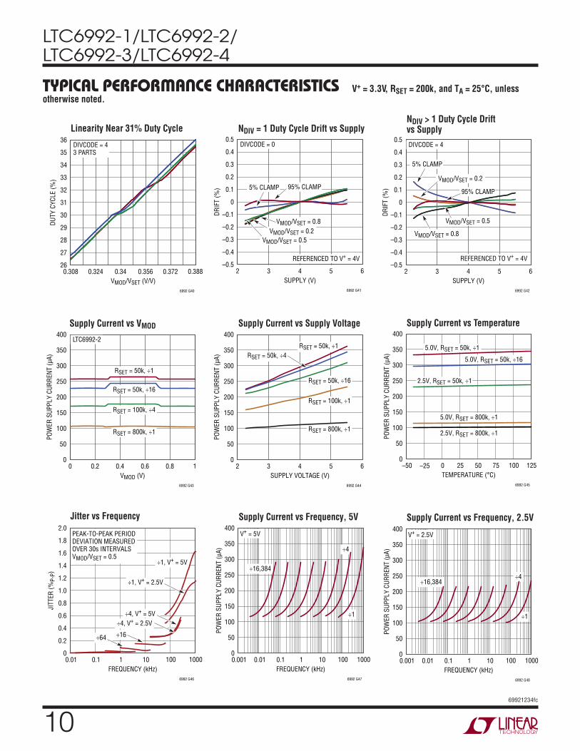
Linearity Near 31% Duty Cycle NDIV = 1 Duty Cycle Drift vs SupplyNDIV > 1 Duty Cycle Drift vs Supply
Supply Current vs VMOD
VMOD/VSET (V/V)
26
31
35
34
33
32
36
0.324 0.34 0.356 0.3720.308 0.388
30
29
28
27
6992 G40
DUTY
CYC
LE (%
)
DIVCODE = 43 PARTS
SUPPLY (V)
–0.5
0
0.4
0.3
0.2
0.1
0.5
3 4 52 6
–0.1
–0.2
–0.3
–0.4
6992 G41
DRIF
T (%
)
DIVCODE = 0
VMOD/VSET = 0.5VMOD/VSET = 0.2
VMOD/VSET = 0.8
5% CLAMP 95% CLAMP
REFERENCED TO V+ = 4V
SUPPLY (V)
–0.5
0
0.4
0.3
0.2
0.1
0.5
3 4 52 6
–0.1
–0.2
–0.3
–0.4
6992 G42
DRIF
T (%
)
DIVCODE = 4
REFERENCED TO V+ = 4V
VMOD/VSET = 0.5
VMOD/VSET = 0.2
VMOD/VSET = 0.8
5% CLAMP
95% CLAMP
V+ = 3.3V, RSET = 200k, and TA = 25°C, unless otherwise noted.
VMOD (V)
0
250
350
300
400
0.40.2 0.6 0.80 1
200
150
100
50
6992 G43
POW
ER S
UPPL
Y CU
RREN
T (µ
A)
LTC6992-2
RSET = 50k, ÷1
RSET = 50k, ÷16
RSET = 100k, ÷4
RSET = 800k, ÷1
Supply Current vs Frequency, 5V Supply Current vs Frequency, 2.5V
Supply Current vs Supply Voltage Supply Current vs Temperature
Jitter vs Frequency
SUPPLY VOLTAGE (V)
0
250
350
300
400
3 4 52 6
200
150
100
50
6992 G44
POW
ER S
UPPL
Y CU
RREN
T (µ
A)
RSET = 50k, ÷1RSET = 50k, ÷4
RSET = 50k, ÷16
RSET = 100k, ÷1
RSET = 800k, ÷1
TEMPERATURE (°C)–50
0
250
300
350
400
0 25 50 100 125
200
150
100
50
–25 75
6992 G45
POW
ER S
UPPL
Y CU
RREN
T (µ
A)
5.0V, RSET = 50k, ÷1
2.5V, RSET = 50k, ÷1
5.0V, RSET = 50k, ÷16
5.0V, RSET = 800k, ÷1
2.5V, RSET = 800k, ÷1
FREQUENCY (kHz)0.01
0
1.4
1.6
1.8
2.0
0.1 1 100 1000
1.2
1.0
0.8
0.6
0.4
0.2
10
6992 G46
JITT
ER (%
P-P)
÷1, V+ = 5V
÷1, V+ = 2.5V
÷4, V+ = 5V÷4, V+ = 2.5V
÷16÷64
PEAK-TO-PEAK PERIODDEVIATION MEASUREDOVER 30s INTERVALSVMOD/VSET = 0.5
FREQUENCY (kHz)0.0010
250
300
350
400
0.10.01 1 100 1000
200
150
100
50
10
6992 G47
POW
ER S
UPPL
Y CU
RREN
T (µ
A) ÷4
÷1
÷16,384
V+ = 5V
FREQUENCY (kHz)0.0010
250
300
350
400
0.10.01 1 100 1000
200
150
100
50
10
6992 G48
POW
ER S
UPPL
Y CU
RREN
T (µ
A)
÷4
÷1
÷16,384
V+ = 2.5V

LTC6992-1/LTC6992-2/LTC6992-3/LTC6992-4
1169921234fc
Typical perForMance characTerisTics
Output Resistance vs Supply Voltage
Rise and Fall Time vs Supply Voltage
Typical ISET Current Limit vs V+
SUPPLY VOLTAGE (V)
RISE
/FAL
L TI
ME
(ns)
6992 G51
3.0
1.5
2.5
1.0
0.5
2.0
02 43 5 6
CLOAD = 5pF
tRISE
tFALL
SUPPLY VOLTAGE (V)
OUTP
UT R
ESIS
TANC
E (Ω
)
6992 G50
50
25
20
35
45
5
10
15
30
40
02 43 5 6
OUTPUT SOURCING CURRENT
OUTPUT SINKING CURRENT
SUPPLY VOLTAGE (V)
I SET
(µA)
6992 G52
1000
400
800
200
600
02 43 5 6
SET PIN SHORTED TO GND
V+ = 3.3V, RSET = 200k, and TA = 25°C, unless otherwise noted.
Typical Start-Up, POL = 0
Typical Start-Up, POL = 1
V+
1V/DIV
OUT1V/DIV
V+ = 2.5VDIVCODE = 3 (÷64)RSET = 50kVMOD = 0.3V (~25% DUTY CYCLE)
100µs/DIV 6992 G53
500µs
V+
1V/DIV
OUT1V/DIV
V+ = 2.5VDIVCODE = 12 (÷64, POL = 1)RSET = 50kVMOD = 0.2V (~87.5% DUTY CYCLE)
100µs/DIV 6992 G54
500µs
125kHz Full Modulation
VMOD0.5V/DIV
OUT1V/DIV
V+ = 3.3VDIVCODE = 1RSET = 100k
50µs/DIV 6992 G55
LTC6992-1
Typical Frequency Error vs Time (Long-Term Drift)
TIME (h)
DELT
A FR
EQUE
NCY
(ppm
)
6992 G48a
50
0
150
–150
–100
–50
100
200
–2000 1200400 800 1600 2000 2400 2800
65 UNITSSOT-23 AND DFN PARTSTA = 30°C
LTC6992-1/LTC6992-2/LTC6992-3/LTC6992-4
1269921234fc
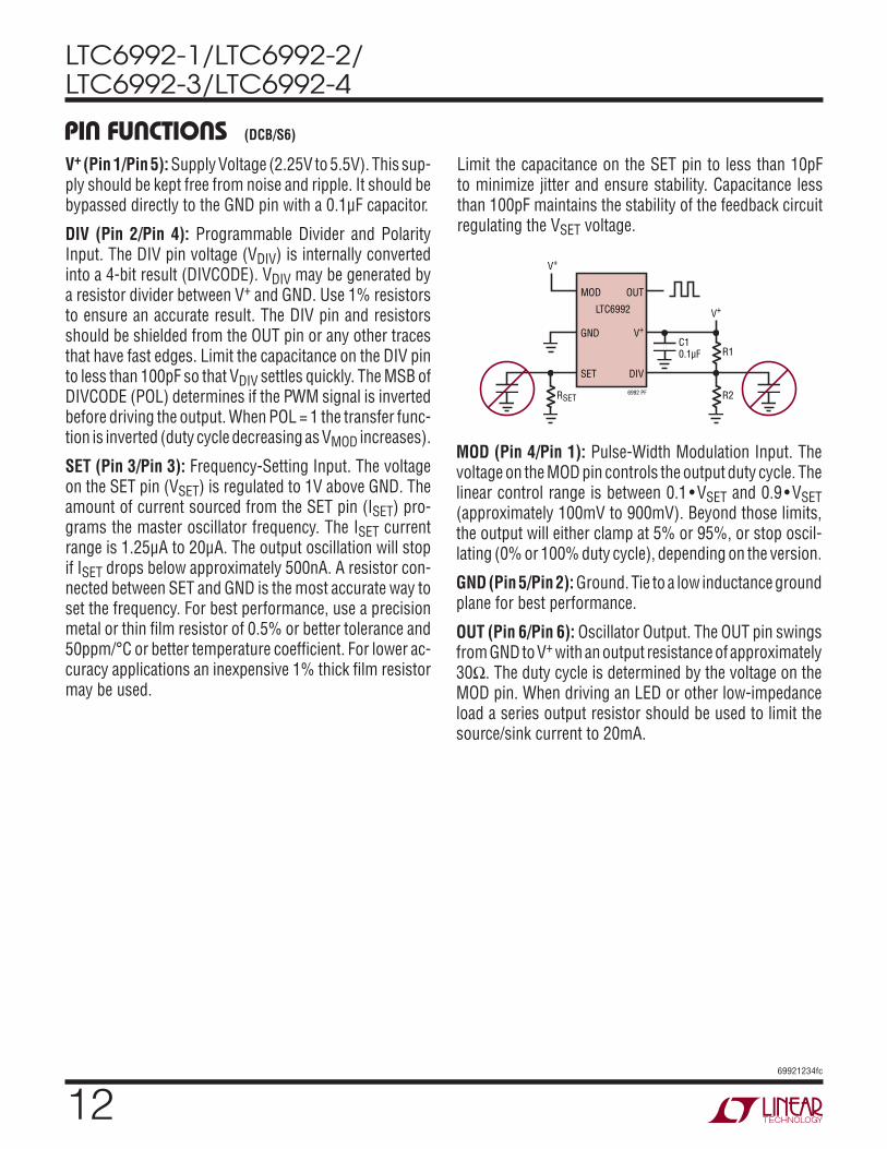
pin FuncTionsV+ (Pin 1/Pin 5): Supply Voltage (2.25V to 5.5V). This sup-ply should be kept free from noise and ripple. It should be bypassed directly to the GND pin with a 0.1μF capacitor.
DIV (Pin 2/Pin 4): Programmable Divider and Polarity Input. The DIV pin voltage (VDIV) is internally converted into a 4-bit result (DIVCODE). VDIV may be generated by a resistor divider between V+ and GND. Use 1% resistors to ensure an accurate result. The DIV pin and resistors should be shielded from the OUT pin or any other traces that have fast edges. Limit the capacitance on the DIV pin to less than 100pF so that VDIV settles quickly. The MSB of DIVCODE (POL) determines if the PWM signal is inverted before driving the output. When POL = 1 the transfer func-tion is inverted (duty cycle decreasing as VMOD increases).
SET (Pin 3/Pin 3): Frequency-Setting Input. The voltage on the SET pin (VSET) is regulated to 1V above GND. The amount of current sourced from the SET pin (ISET) pro-grams the master oscillator frequency. The ISET current range is 1.25μA to 20μA. The output oscillation will stop if ISET drops below approximately 500nA. A resistor con-nected between SET and GND is the most accurate way to set the frequency. For best performance, use a precision metal or thin film resistor of 0.5% or better tolerance and 50ppm/°C or better temperature coefficient. For lower ac-curacy applications an inexpensive 1% thick film resistor may be used.
Limit the capacitance on the SET pin to less than 10pF to minimize jitter and ensure stability. Capacitance less than 100pF maintains the stability of the feedback circuit regulating the VSET voltage.
(DCB/S6)
6992 PF
LTC6992
MOD
GND
SET
OUT
V+
DIV
C10.1µF
RSET R2
R1
V+
V+
MOD (Pin 4/Pin 1): Pulse-Width Modulation Input. The voltage on the MOD pin controls the output duty cycle. The linear control range is between 0.1 • VSET and 0.9 • VSET (approximately 100mV to 900mV). Beyond those limits, the output will either clamp at 5% or 95%, or stop oscil-lating (0% or 100% duty cycle), depending on the version.
GND (Pin 5/Pin 2): Ground. Tie to a low inductance ground plane for best performance.
OUT (Pin 6/Pin 6): Oscillator Output. The OUT pin swings from GND to V+ with an output resistance of approximately 30Ω. The duty cycle is determined by the voltage on the MOD pin. When driving an LED or other low-impedance load a series output resistor should be used to limit the source/sink current to 20mA.
LTC6992-1/LTC6992-2/LTC6992-3/LTC6992-4
1369921234fc
block DiagraM (S6 Package Pin Numbers Shown)
6992 BD
PROGRAMMABLE DIVIDER÷1, 4, 16, 64, 256, 1024, 4096, 16384
MASTER OSCILLATOR
DISABLE OUTPUTUNTIL SETTLED
POR
OUTPUTPOLARITY
DIGITALFILTER
4-BIT A/DCONVERTER
fOSC = 1MHz • 50kΩ •ISETVSET
POLR1
R2
DIV
V+
OUT
D = tONtOUT
5
4
1
6
HALT OSCILLATORIF ISET < 500nA
MCLK
+–
ISET
VSET = 1V +–VREF1V
3 22GNDSET MOD
RSET
DUTY CYCLE =VMOD(LIM) – 0.1•VSET
0.8•VSET
VOLTAGE LIMITER
VMOD(LIM)
VMOD
PULSE WIDTH MODULATOR
tOUT
tON

LTC6992-1/LTC6992-2/LTC6992-3/LTC6992-4
1469921234fc
operaTionThe LTC6992 is built around a master oscillator with a 1MHz maximum frequency. The oscillator is controlled by the SET pin current (ISET) and voltage (VSET), with a 1MHz • 50k conversion factor that is accurate to ±0.8% under typical conditions.
fMASTER = 1
tMASTER= 1MHz • 50k •
ISETVSET
A feedback loop maintains VSET at 1V ±30mV, leaving ISET as the primary means of controlling the output frequency. The simplest way to generate ISET is to connect a resistor (RSET) between SET and GND, such that ISET = VSET/RSET. The master oscillator equation reduces to:
fMASTER = 1
tMASTER= 1MHz • 50k
RSET
From this equation, it is clear that VSET drift will not affect the output frequency when using a single program resistor (RSET). Error sources are limited to RSET tolerance and the inherent frequency accuracy ∆fOUT of the LTC6992.
RSET may range from 50k to 800k (equivalent to ISET between 1.25μA and 20μA).
The LTC6992 includes a programmable frequency divider which can further divide the frequency by 1, 4, 16, 64, 256, 1024, 4096 or 16384 before driving the OUT pin. The divider ratio NDIV is set by a resistor divider attached to the DIV pin.
fOUT = 1
tOUT= 1MHz • 50k
NDIV•
ISETVSET
With RSET in place of VSET/ISET the equation reduces to:
fOUT =
1tOUT
= 1MHz • 50kNDIV •RSET
DIVCODE
The DIV pin connects to an internal, V+ referenced 4-bit A/D converter that determines the DIVCODE value. DIVCODE programs two settings on the LTC6992:
1. DIVCODE determines the output frequency divider set-ting, NDIV.
2. DIVCODE determines the output polarity, via the POL bit.
VDIV may be generated by a resistor divider between V+ and GND as shown in Figure 1.
Figure 1. Simple Technique for Setting DIVCODE
6992 F01
LTC6992
V+
DIV
GND
R1
R2
2.25V TO 5.5V
LTC6992-1/LTC6992-2/LTC6992-3/LTC6992-4
1569921234fc
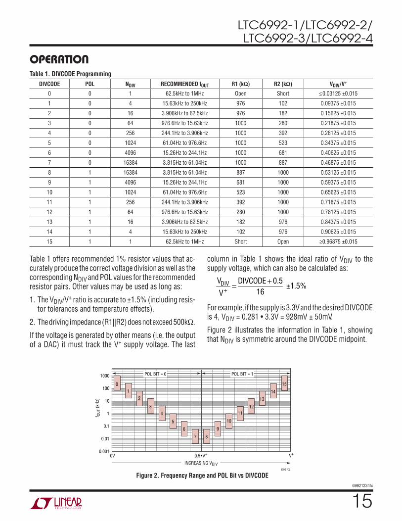
Table 1 offers recommended 1% resistor values that ac-curately produce the correct voltage division as well as the corresponding NDIV and POL values for the recommended resistor pairs. Other values may be used as long as:
1. The VDIV/V+ ratio is accurate to ±1.5% (including resis-tor tolerances and temperature effects).
2. The driving impedance (R1||R2) does not exceed 500kΩ.
If the voltage is generated by other means (i.e. the output of a DAC) it must track the V+ supply voltage. The last
column in Table 1 shows the ideal ratio of VDIV to the supply voltage, which can also be calculated as:
VDIV
V+ = DIVCODE + 0.516
±1.5%
For example, if the supply is 3.3V and the desired DIVCODE is 4, VDIV = 0.281 • 3.3V = 928mV ± 50mV.
Figure 2 illustrates the information in Table 1, showing that NDIV is symmetric around the DIVCODE midpoint.
Table 1. DIVCODE ProgrammingDIVCODE POL NDIV RECOMMENDED fOUT R1 (kΩ) R2 (kΩ) VDIV/V+
0 0 1 62.5kHz to 1MHz Open Short ≤0.03125 ±0.015
1 0 4 15.63kHz to 250kHz 976 102 0.09375 ±0.015
2 0 16 3.906kHz to 62.5kHz 976 182 0.15625 ±0.015
3 0 64 976.6Hz to 15.63kHz 1000 280 0.21875 ±0.015
4 0 256 244.1Hz to 3.906kHz 1000 392 0.28125 ±0.015
5 0 1024 61.04Hz to 976.6Hz 1000 523 0.34375 ±0.015
6 0 4096 15.26Hz to 244.1Hz 1000 681 0.40625 ±0.015
7 0 16384 3.815Hz to 61.04Hz 1000 887 0.46875 ±0.015
8 1 16384 3.815Hz to 61.04Hz 887 1000 0.53125 ±0.015
9 1 4096 15.26Hz to 244.1Hz 681 1000 0.59375 ±0.015
10 1 1024 61.04Hz to 976.6Hz 523 1000 0.65625 ±0.015
11 1 256 244.1Hz to 3.906kHz 392 1000 0.71875 ±0.015
12 1 64 976.6Hz to 15.63kHz 280 1000 0.78125 ±0.015
13 1 16 3.906kHz to 62.5kHz 182 976 0.84375 ±0.015
14 1 4 15.63kHz to 250kHz 102 976 0.90625 ±0.015
15 1 1 62.5kHz to 1MHz Short Open ≥0.96875 ±0.015
operaTion
Figure 2. Frequency Range and POL Bit vs DIVCODE
0.5•V+
f OUT
(kHz
)
6992 F02
1000
100
10
1
0.001
0.1
0.01
INCREASING VDIV
V+0V
POL BIT = 0 POL BIT = 1
0 151
3
2
5
4
7
6 9
8
11
10
13
12
14
LTC6992-1/LTC6992-2/LTC6992-3/LTC6992-4
1669921234fc
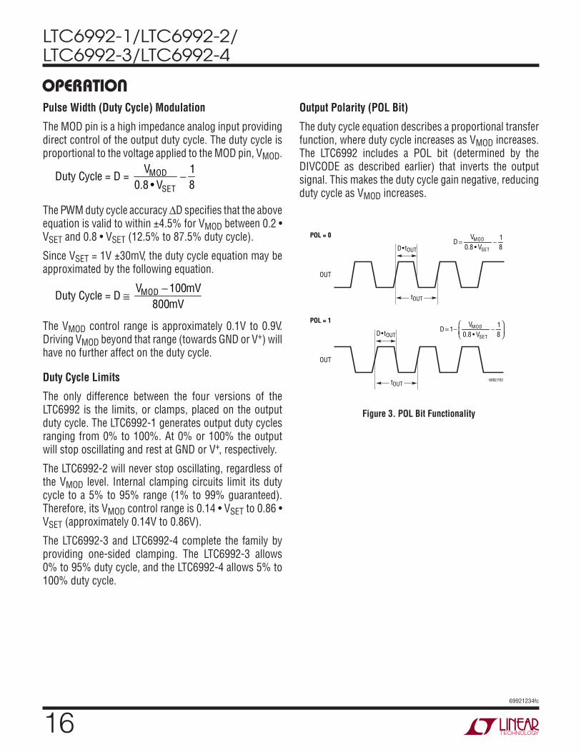
Pulse Width (Duty Cycle) Modulation
The MOD pin is a high impedance analog input providing direct control of the output duty cycle. The duty cycle is proportional to the voltage applied to the MOD pin, VMOD.
Duty Cycle = D =
VMOD0.8 • VSET
− 18
The PWM duty cycle accuracy ∆D specifies that the above equation is valid to within ±4.5% for VMOD between 0.2 • VSET and 0.8 • VSET (12.5% to 87.5% duty cycle).
Since VSET = 1V ±30mV, the duty cycle equation may be approximated by the following equation.
Duty Cycle = D ≅
VMOD − 100mV800mV
The VMOD control range is approximately 0.1V to 0.9V. Driving VMOD beyond that range (towards GND or V+) will have no further affect on the duty cycle.
Duty Cycle Limits
The only difference between the four versions of the LTC6992 is the limits, or clamps, placed on the output duty cycle. The LTC6992-1 generates output duty cycles ranging from 0% to 100%. At 0% or 100% the output will stop oscillating and rest at GND or V+, respectively.
The LTC6992-2 will never stop oscillating, regardless of the VMOD level. Internal clamping circuits limit its duty cycle to a 5% to 95% range (1% to 99% guaranteed). Therefore, its VMOD control range is 0.14 • VSET to 0.86 • VSET (approximately 0.14V to 0.86V).
The LTC6992-3 and LTC6992-4 complete the family by providing one-sided clamping. The LTC6992-3 allows 0% to 95% duty cycle, and the LTC6992-4 allows 5% to 100% duty cycle.
Output Polarity (POL Bit)
The duty cycle equation describes a proportional transfer function, where duty cycle increases as VMOD increases. The LTC6992 includes a POL bit (determined by the DIVCODE as described earlier) that inverts the output signal. This makes the duty cycle gain negative, reducing duty cycle as VMOD increases.
operaTion
Figure 3. POL Bit Functionality
6992 F03
OUT
POL = 1
tOUT
D • tOUT
OUT
POL = 0
tOUT
D • tOUT D =
VMOD
0.8 • VSET−
18
D = 1−VMOD
0.8 • VSET−
18

LTC6992-1/LTC6992-2/LTC6992-3/LTC6992-4
1769921234fc
POL = 1 forces a simple logic inversion, so it changes the duty cycle range of the LTC6992-3 (making it 100% to 5%) and LTC6992-4 (making it 95% to 0%). These transfer functions are detailed in Figure 4.
Table 2. Duty Cycle Ranges
PART NUMBER
DUTY CYCLE RANGE vs VMOD = 0V → 1V
POL = 0 POL = 1
LTC6992-1 0% to 100% 100% to 0%
LTC6992-2 5% to 95% 95% to 5%
LTC6992-3 0% to 95% 100% to 5%
LTC6992-4 5% to 100% 95% to 0%
operaTion
Figure 4. PWM Transfer Functions for All LTC6992 Family Parts
VMOD/VSET (V/V)0
DUTY
CYC
LE (%
)
100
90
60
40
20
70
80
50
30
10
00.4 0.8 0.90.2 0.6
6992 F04a
VMOD/VSET = 0.9
VMOD/VSET = 0.1
10.3 0.70.1 0.5
POL = 1 POL = 0
VMOD/VSET (V/V)0
DUTY
CYC
LE (%
)
100
90
60
40
20
70
80
50
30
10
00.4 0.8 0.90.2 0.6
6992 F04b
10.3 0.70.1 0.5
POL = 1 POL = 0
VMOD/VSET = 0.86
VMOD/VSET = 0.14
VMOD/VSET (V/V)0
DUTY
CYC
LE (%
)
100
90
60
40
20
70
80
50
30
10
00.4 0.8 0.90.2 0.6
6992 F02c
10.3 0.70.1 0.5
POL = 1 POL = 0
VMOD/VSET = 0.1
VMOD/VSET = 0.86
VMOD/VSET (V/V)0
DUTY
CYC
LE (%
)
100
90
60
40
20
70
80
50
30
10
00.4 0.8 0.90.2 0.6
6992 F02d
10.3 0.70.1 0.5
POL = 1 POL = 0
VMOD/VSET = 0.9
VMOD/VSET = 0.14
LTC6992-1 LTC6992-2
LTC6992-3 LTC6992-4
LTC6992-1/LTC6992-2/LTC6992-3/LTC6992-4
1869921234fc
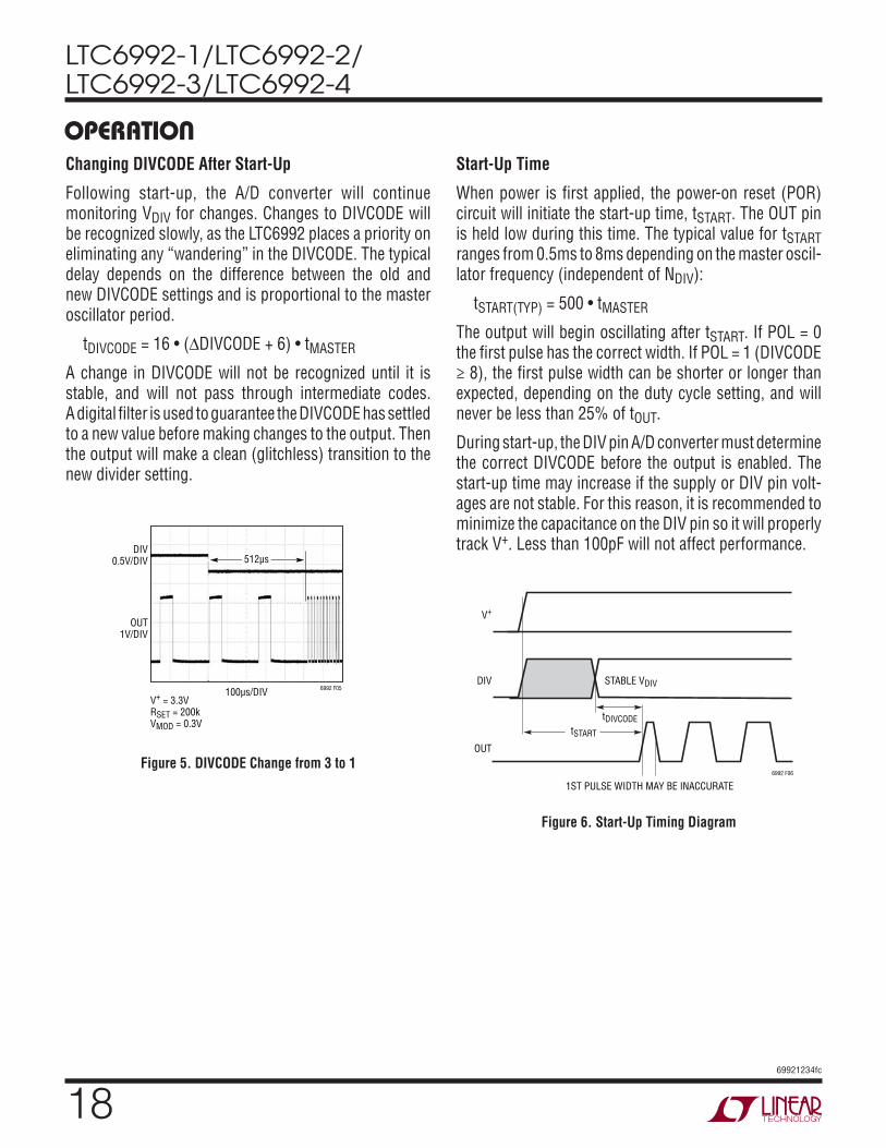
Changing DIVCODE After Start-Up
Following start-up, the A/D converter will continue monitoring VDIV for changes. Changes to DIVCODE will be recognized slowly, as the LTC6992 places a priority on eliminating any “wandering” in the DIVCODE. The typical delay depends on the difference between the old and new DIVCODE settings and is proportional to the master oscillator period.
tDIVCODE = 16 • (∆DIVCODE + 6) • tMASTER
A change in DIVCODE will not be recognized until it is stable, and will not pass through intermediate codes. A digital filter is used to guarantee the DIVCODE has settled to a new value before making changes to the output. Then the output will make a clean (glitchless) transition to the new divider setting.
operaTionStart-Up Time
When power is first applied, the power-on reset (POR) circuit will initiate the start-up time, tSTART. The OUT pin is held low during this time. The typical value for tSTART ranges from 0.5ms to 8ms depending on the master oscil-lator frequency (independent of NDIV):
tSTART(TYP) = 500 • tMASTER
The output will begin oscillating after tSTART. If POL = 0 the first pulse has the correct width. If POL = 1 (DIVCODE ≥ 8), the first pulse width can be shorter or longer than expected, depending on the duty cycle setting, and will never be less than 25% of tOUT.
During start-up, the DIV pin A/D converter must determine the correct DIVCODE before the output is enabled. The start-up time may increase if the supply or DIV pin volt-ages are not stable. For this reason, it is recommended to minimize the capacitance on the DIV pin so it will properly track V+. Less than 100pF will not affect performance.
6992 F06
OUT
DIV STABLE VDIV
V+
tDIVCODEtSTART
1ST PULSE WIDTH MAY BE INACCURATE
Figure 5. DIVCODE Change from 3 to 1
Figure 6. Start-Up Timing Diagram
DIV0.5V/DIV
OUT1V/DIV
V+ = 3.3VRSET = 200kVMOD = 0.3V
100µs/DIV 6992 F05
512µs
LTC6992-1/LTC6992-2/LTC6992-3/LTC6992-4
1969921234fc
Basic Operation
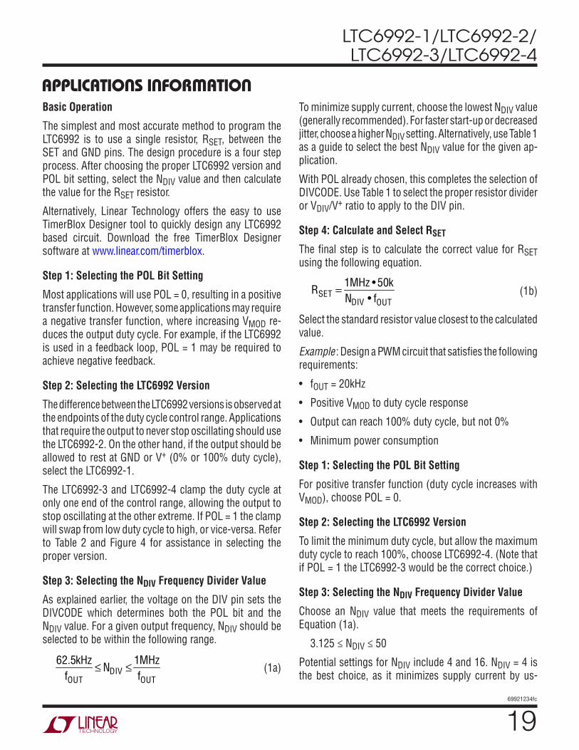
The simplest and most accurate method to program the LTC6992 is to use a single resistor, RSET, between the SET and GND pins. The design procedure is a four step process. After choosing the proper LTC6992 version and POL bit setting, select the NDIV value and then calculate the value for the RSET resistor.
Alternatively, Linear Technology offers the easy to use TimerBlox Designer tool to quickly design any LTC6992 based circuit. Download the free TimerBlox Designer software at www.linear.com/timerblox.
Step 1: Selecting the POL Bit Setting
Most applications will use POL = 0, resulting in a positive transfer function. However, some applications may require a negative transfer function, where increasing VMOD re-duces the output duty cycle. For example, if the LTC6992 is used in a feedback loop, POL = 1 may be required to achieve negative feedback.
Step 2: Selecting the LTC6992 Version
The difference between the LTC6992 versions is observed at the endpoints of the duty cycle control range. Applications that require the output to never stop oscillating should use the LTC6992-2. On the other hand, if the output should be allowed to rest at GND or V+ (0% or 100% duty cycle), select the LTC6992-1.
The LTC6992-3 and LTC6992-4 clamp the duty cycle at only one end of the control range, allowing the output to stop oscillating at the other extreme. If POL = 1 the clamp will swap from low duty cycle to high, or vice-versa. Refer to Table 2 and Figure 4 for assistance in selecting the proper version.
Step 3: Selecting the NDIV Frequency Divider Value
As explained earlier, the voltage on the DIV pin sets the DIVCODE which determines both the POL bit and the NDIV value. For a given output frequency, NDIV should be selected to be within the following range.
62.5kHzfOUT
≤ NDIV ≤ 1MHzfOUT
(1a)
applicaTions inForMaTionTo minimize supply current, choose the lowest NDIV value (generally recommended). For faster start-up or decreased jitter, choose a higher NDIV setting. Alternatively, use Table 1 as a guide to select the best NDIV value for the given ap-plication.
With POL already chosen, this completes the selection of DIVCODE. Use Table 1 to select the proper resistor divider or VDIV/V+ ratio to apply to the DIV pin.
Step 4: Calculate and Select RSET
The final step is to calculate the correct value for RSET using the following equation.
RSET = 1MHz • 50k
NDIV • fOUT (1b)
Select the standard resistor value closest to the calculated value.
Example : Design a PWM circuit that satisfies the following requirements:
• fOUT = 20kHz
• Positive VMOD to duty cycle response
• Output can reach 100% duty cycle, but not 0%
• Minimum power consumption
Step 1: Selecting the POL Bit Setting
For positive transfer function (duty cycle increases with VMOD), choose POL = 0.
Step 2: Selecting the LTC6992 Version
To limit the minimum duty cycle, but allow the maximum duty cycle to reach 100%, choose LTC6992-4. (Note that if POL = 1 the LTC6992-3 would be the correct choice.)
Step 3: Selecting the NDIV Frequency Divider Value
Choose an NDIV value that meets the requirements of Equation (1a).
3.125 ≤ NDIV ≤ 50
Potential settings for NDIV include 4 and 16. NDIV = 4 is the best choice, as it minimizes supply current by us-
LTC6992-1/LTC6992-2/LTC6992-3/LTC6992-4
2069921234fc
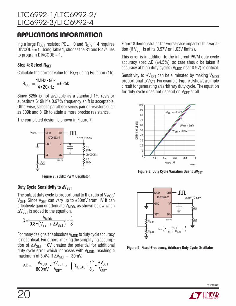
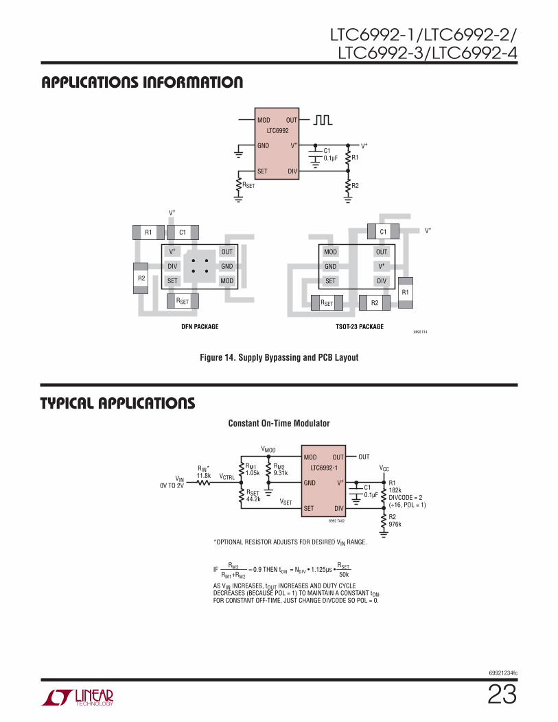
applicaTions inForMaTioning a large RSET resistor. POL = 0 and NDIV = 4 requires DIVCODE = 1. Using Table 1, choose the R1 and R2 values to program DIVCODE = 1.
Step 4: Select RSET
Calculate the correct value for RSET using Equation (1b).
RSET = 1MHz • 50k
4 • 20kHz= 625k
Since 625k is not available as a standard 1% resistor, substitute 619k if a 0.97% frequency shift is acceptable. Otherwise, select a parallel or series pair of resistors such as 309k and 316k to attain a more precise resistance.
The completed design is shown in Figure 7.
6992 F07
LTC6992-4
MOD
GND
SET
OUT
V+
DIV
R1976k
DIVCODE = 1
R2102kRSET
625k
VMOD
2.25V TO 5.5V
Figure 7. 20kHz PWM OscillatorFigure 8. Duty Cycle Variation Due to ∆VSET
VMOD (V)0
DUTY
CYC
LE (%
)
100
90
70
80
60
50
30
40
20
10
00.60.2
6992 F08
10.4 0.8
∆VSET = 0mV
∆VSET = 30mV
∆VSET = –30mV
Figure 9. Fixed-Frequency, Arbitrary Duty Cycle Oscillator
6992 F09
LTC6992-X
MOD
GND
SET
OUT
V+
DIV
R1
R2
RSET2
RSET1
2.25V TO 5.5V
D =
54
•RSET2
RSET1 +RSET2−
18
Figure 8 demonstrates the worst-case impact of this varia-tion (if VSET is at its 0.97V or 1.03V limits).
This error is in addition to the inherent PWM duty cycle accuracy spec ∆D (±4.5%), so care should be taken if accuracy at high duty cycles (VMOD near 0.9V) is critical.
Sensitivity to ∆VSET can be eliminated by making VMOD proportional to VSET. For example, Figure 9 shows a simple circuit for generating an arbitrary duty cycle. The equation for duty cycle does not depend on VSET at all.
Duty Cycle Sensitivity to ∆VSET
The output duty cycle is proportional to the ratio of VMOD/VSET. Since VSET can vary up to ±30mV from 1V it can effectively gain or attenuate VMOD, as shown below when ∆VSET is added to the equation.
D =
VMOD0.8 • VSET + ∆VSET( ) − 1
8
For many designs, the absolute VMOD to duty cycle accuracy is not critical. For others, making the simplifying assump-tion of ∆VSET = 0V creates the potential for additional duty cycle error, which increases with VMOD, reaching a maximum of 3.4% if ∆VSET = –30mV.
∆D≅ − VMOD
800mV•
∆VSETVSET
≅ − DIDEAL + 18
•
∆VSETVSET
LTC6992-1/LTC6992-2/LTC6992-3/LTC6992-4
2169921234fc
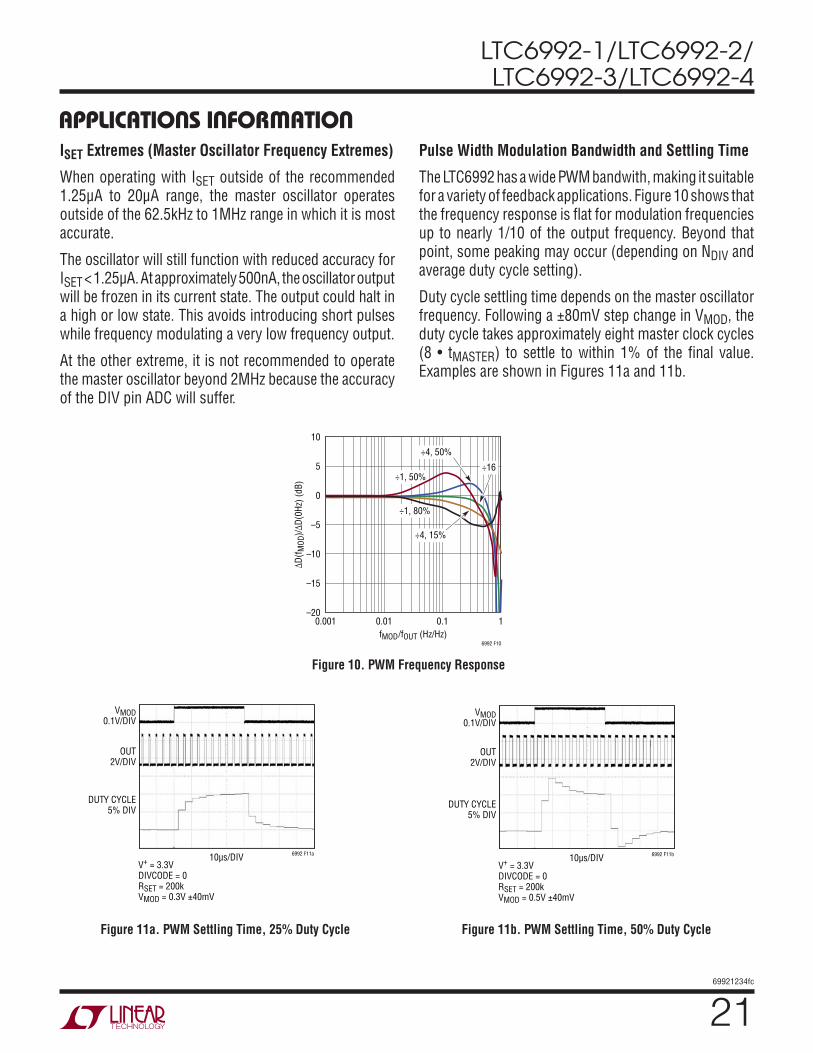
applicaTions inForMaTionISET Extremes (Master Oscillator Frequency Extremes)
When operating with ISET outside of the recommended 1.25μA to 20μA range, the master oscillator operates outside of the 62.5kHz to 1MHz range in which it is most accurate.
The oscillator will still function with reduced accuracy for ISET < 1.25µA. At approximately 500nA, the oscillator output will be frozen in its current state. The output could halt in a high or low state. This avoids introducing short pulses while frequency modulating a very low frequency output.
At the other extreme, it is not recommended to operate the master oscillator beyond 2MHz because the accuracy of the DIV pin ADC will suffer.
Pulse Width Modulation Bandwidth and Settling Time
The LTC6992 has a wide PWM bandwith, making it suitable for a variety of feedback applications. Figure 10 shows that the frequency response is flat for modulation frequencies up to nearly 1/10 of the output frequency. Beyond that point, some peaking may occur (depending on NDIV and average duty cycle setting).
Duty cycle settling time depends on the master oscillator frequency. Following a ±80mV step change in VMOD, the duty cycle takes approximately eight master clock cycles (8 • tMASTER) to settle to within 1% of the final value. Examples are shown in Figures 11a and 11b.
Figure 10. PWM Frequency Response
Figure 11a. PWM Settling Time, 25% Duty Cycle Figure 11b. PWM Settling Time, 50% Duty Cycle
fMOD/fOUT (Hz/Hz)0.001
∆D(f M
OD)/∆
D(0H
z) (d
B)
10
5
–5
0
–10
–15
–200.01
6992 F10
10.1
÷1, 50%
÷1, 80%
÷16
÷4, 50%
÷4, 15%
VMOD0.1V/DIV
OUT2V/DIV
DUTY CYCLE5% DIV
V+ = 3.3VDIVCODE = 0RSET = 200kVMOD = 0.3V ±40mV
10µs/DIV 6992 F11a
VMOD0.1V/DIV
OUT2V/DIV
DUTY CYCLE5% DIV
V+ = 3.3VDIVCODE = 0RSET = 200kVMOD = 0.5V ±40mV
10µs/DIV 6992 F11b

LTC6992-1/LTC6992-2/LTC6992-3/LTC6992-4
2269921234fc
Power Supply Current
The power supply current varies with frequency, supply voltage and output loading. It can be estimated under any condition using the following equation:
If NDIV = 1 (DIVCODE = 0 or 15):
IS(TYP) ≈ V+ • fOUT • 39pF + CLOAD( )
+ V+
320kΩ+ V+ •Duty Cycle
RLOAD+ 2.2 • ISET + 85µA
If NDIV > 1 (DIVCODE = 1 or 14):
IS(TYP) ≈ V+ • NDIV • fOUT • 27pF
+ V+ • fOUT • 28pF + CLOAD( )
+ V+
320kΩ+ V+ •Duty Cycle
RLOAD+ 2.6 • ISET + 90µA
SUPPLY BYPASSING AND PCB LAYOUT GUIDELINES
The LTC6992 is a 2.4% accurate silicon oscillator when used in the appropriate manner. The part is simple to use and by following a few rules, the expected performance is easily achieved. Adequate supply bypassing and proper PCB layout are important to ensure this.
Figure 14 shows example PCB layouts for both the TSOT-23 and DFN packages using 0603 sized passive components. The layouts assume a two layer board with a ground plane layer beneath and around the LTC6992. These layouts are a guide and need not be followed exactly.
applicaTions inForMaTion1. Connect the bypass capacitor, C1, directly to the V+ and
GND pins using a low inductance path. The connection from C1 to the V+ pin is easily done directly on the top layer. For the DFN package, C1’s connection to GND is also simply done on the top layer. For the TSOT-23, OUT can be routed through the C1 pads to allow a good C1 GND connection. If the PCB design rules do not allow that, C1’s GND connection can be accomplished through multiple vias to the ground plane. Multiple vias for both the GND pin connection to the ground plane and the C1 connection to the ground plane are recommended to minimize the inductance. Capacitor C1 should be a 0.1μF ceramic capacitor.
2. Place all passive components on the top side of the board. This minimizes trace inductance.
3. Place RSET as close as possible to the SET pin and make a direct, short connection. The SET pin is a current summing node and currents injected into this pin directly modulate the operating frequency. Having a short connection minimizes the exposure to signal pickup.
4. Connect RSET directly to the GND pin. Using a long path or vias to the ground plane will not have a significant affect on accuracy, but a direct, short connection is recommended and easy to apply.
5. Use a ground trace to shield the SET pin. This provides another layer of protection from radiated signals.
6. Place R1 and R2 close to the DIV pin. A direct, short connection to the DIV pin minimizes the external signal coupling.
LTC6992-1/LTC6992-2/LTC6992-3/LTC6992-4
2369921234fc
Typical applicaTions
Figure 14. Supply Bypassing and PCB Layout
Constant On-Time Modulator
6992 TA02
LTC6992-1
MOD
GND
SET
OUT
V+
DIV
RM29.31k
RM11.05k
RSET44.2k
RIN*11.8k VCTRL
VMOD
VSET
VIN0V TO 2V R1
182kDIVCODE = 2(÷16, POL = 1)
C10.1µF
OUT
R2976k
VCC
*OPTIONAL RESISTOR ADJUSTS FOR DESIRED VIN RANGE.
AS VIN INCREASES, tOUT INCREASES AND DUTY CYCLE DECREASES (BECAUSE POL = 1) TO MAINTAIN A CONSTANT tON.FOR CONSTANT OFF-TIME, JUST CHANGE DIVCODE SO POL = 0.
IF
RM2
RM1+RM2= 0.9 THEN tON = NDIV • 1.125µs •
RSET
50k
applicaTions inForMaTion
6992 F14
LTC6992
MOD
GND
SET
OUT
V+
DIV
C10.1µF R1
R2RSET
V+
MOD
GND
SET
OUT
V+
DIV
V+
DIV
SET
OUT
GND
MOD
R1
R2
C1
RSET
V+C1R1
R2
V+
RSET
TSOT-23 PACKAGEDFN PACKAGE
LTC6992-1/LTC6992-2/LTC6992-3/LTC6992-4
2469921234fc
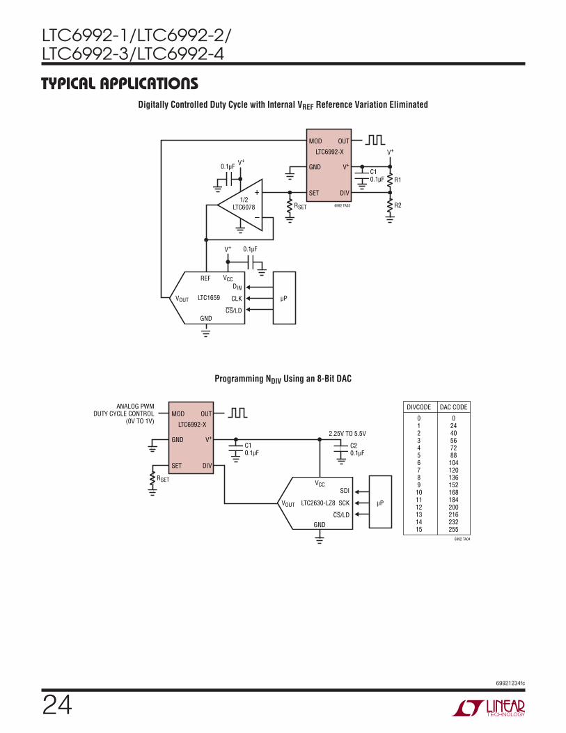
Typical applicaTionsDigitally Controlled Duty Cycle with Internal VREF Reference Variation Eliminated
Programming NDIV Using an 8-Bit DAC
6992 TA03
LTC6992-X
MOD
GND
SET
OUT
V+
DIV
RSET
–
+
V+
1/2LTC6078
R1C10.1µF
R2
LTC1659VOUT CLK µP
CS/LD
DIN
REF VCC
GND
V+
V+
0.1µF
0.1µF
6992 TA04
LTC6992-X
MOD
GND
SET
OUT
V+
DIV
RSET
C10.1µF
LTC2630-LZ8VOUT SCK µP
CS/LD
SDIVCC
GND
2.25V TO 5.5V
C20.1µF
DIVCODE
0123456789101112131415
DAC CODE
02440567288104120136152168184200216232255
ANALOG PWMDUTY CYCLE CONTROL
(0V TO 1V)
LTC6992-1/LTC6992-2/LTC6992-3/LTC6992-4
2569921234fc
Typical applicaTionsChanging Between Two Frequencies
6992 TA05
LTC6992-X
MOD
GND
SET
OUT
V+
DIV
R10.1µF 0.1µF
R2RSET
V+
NOTESWHILE THIS CIRCUIT IS SIMPLER THAN THE CIRCUIT TO THE RIGHT, ITS FREQUENCY ACCURACY IS WORSE DUE TO THE EFFECT OFV+ SUPPLY VARIATION FROM SYSTEM TO SYSTEM AND OVER TEMPERATURE.
NOTES1. WHEN THE NMOSFET IS OFF, THE FREQUENCY IS SET BY RSET = RSET1.2. WHEN THE NMOSFET IS ON, THE FREQUENCY IS SET BY RSET = RSET1 || RSET2.3. V+ SUPPLY VARIATION IS NOT A FACTOR AS THE SWITCHING RESISTOR IS EITHER FLOATING OR CONNECTED TO GROUND.
RVCO
V+
‘HC04
fMAX
fMIN
ANALOG PWMDUTY CYCLE CONTROL
(0V TO 1V)LTC6992-X
MOD
GND
SET
OUT
V+
DIV
R1
R2RSET1RSET2
V+
ANALOG PWMDUTY CYCLE CONTROL
(0V TO 1V)
V+
‘HC042N7002
fMIN
fMAX
Simple Diode Temperature Sensor
6992 TA06
LTC6992-2
MOD
GND
SET
OUT
V+
DIV
R41000k
MOC207M
Q1
OUTPUT
D3
C11µF
R5186k
5V
5V0.1µF
0.1µF
5V
LT6003
+10mV/C
5V
R1130k
R250k
R3130k
ADJUST FOR 50% DUTY CYCLE AT 25°C
+–
R716.9k
R884.5k
R645.3k
D11N458
R11422Ω
NDIV = 16f = 10kHz
PWM OUTPUT FOR ISOLATED MEASUREMENT+1% DUTY CYCLE CHANGE PER DEGREE C–10°C TO 65°C RANGE WITH OPTO-ISOLATOR (DC: 15% TO 95%)
R9365Ω
0.1µF

LTC6992-1/LTC6992-2/LTC6992-3/LTC6992-4
2669921234fc
Motor Speed/Direction Control for Full H-Bridge (Locked Anti-Phase Drive)
Typical applicaTions
6992 TA07
LTC6992-2
MOTOR
A1
A2
CW CURRENTFLOW
VS12V
POWER H-BRIDGEHIGH = SWITCH ON
MOD
GND
SET
OUT
V+
DIV
R11000k 0.1µF
INPUT 0V TO 1V
R2280k
V+
R3300k
2.6kHz, 5% TO 95% PWM5% DC = CLOCKWISE50% DC = STOPPED95% DC = COUNTER CLOCKWISE
Motor Speed/Direction Control for Full H-Bridge (Sign/Magnitude Drive)
6992 TA08
LTC6992-2
MOTOR
A3
A4 A5
CW CURRENTFLOW
VS12V
POWER H-BRIDGEHIGH = SWITCH ON
MOD
GND
SET
OUT
V+
DIV
R41000k
INPUT 0V TO 1V
R5280k
V+
R3300k
2.6kHz, 5% TO 95% PWM5% DC = SLOW95% DC = FAST
DIRECTIONH = CCW, L = CW
0.1µF

LTC6992-1/LTC6992-2/LTC6992-3/LTC6992-4
2769921234fc
Typical applicaTionsRatiometric Sensor to Pulse Width, Non-Inverting Response
6992 TA09
LTC6992-1
C10.15µF
MOD
GND
SET
OUT
V+
DIV
R11000k
R2186k
VS
OUTPUTDUTY CYCLE = K • 100%
VS
LT1490K • VS
VS = 2.5V TO 5.5V
RSET316k
+–R3
10kK = 1
K = 0
R490.9k
R510M
R69.09k
RSENSOR
NDIV = 16fOUT = 10kHz
0.1µF C20.22µF
0.1µF
Ratiometric Sensor to Pulse Width, Inverting Response
6992 TA10
LTC6992-1
C10.15µF
MOD
GND
SET
OUT
V+
DIV
R11000k
R2186k
VS
OUTPUTDUTY CYCLE = (1–K) • 100%
VS
VSLT1490
VS = 2.5V TO 5.5V
RSET316k
+–
R3100k
R410k
K = 1
K = 0
R690.9k
K • VS
R510k
R69.09k
RSENSOR
NDIV = 16fOUT = 10kHz
C20.22µF0.1µF
0.1µF

LTC6992-1/LTC6992-2/LTC6992-3/LTC6992-4
2869921234fc
Typical applicaTionsRadio Control Servo Pulse Generator
6992 TA11
LTC6992-1
C11µF
MOD
GND
SET
OUT
V+
DIV
R11000k
R2681k
VS
OUTPUT1ms TO 2ms PULSE EVERY 16ms
VS
LT1490
VS = 2.5V TO 5.5V
RSET196k
+–
R690.9k
R5130k
R68.66k
SERVOCONTROLPOT10k
2ms
1ms
R69.09k
NDIV = 4096fOUT = 62.5Hz, 16ms PERIOD
C20.22µF
0.1µF
0.1µF
Direct Voltage Controlled PWM Dimming (0 to 15000 Cd/m2 Intensity)
6992 TA12
LTC6992-1
MOD
GND
SET
OUT
V+
DIV
f = 7.5kHzNDIV = 64
5VD1
HIGH INTENSITY LEDSSL-LX5093XUWC
R2280kRSET
105k
VDIMMING
R11M
R390.9Ω
C10.1µF
LTC6992-1/LTC6992-2/LTC6992-3/LTC6992-4
2969921234fc
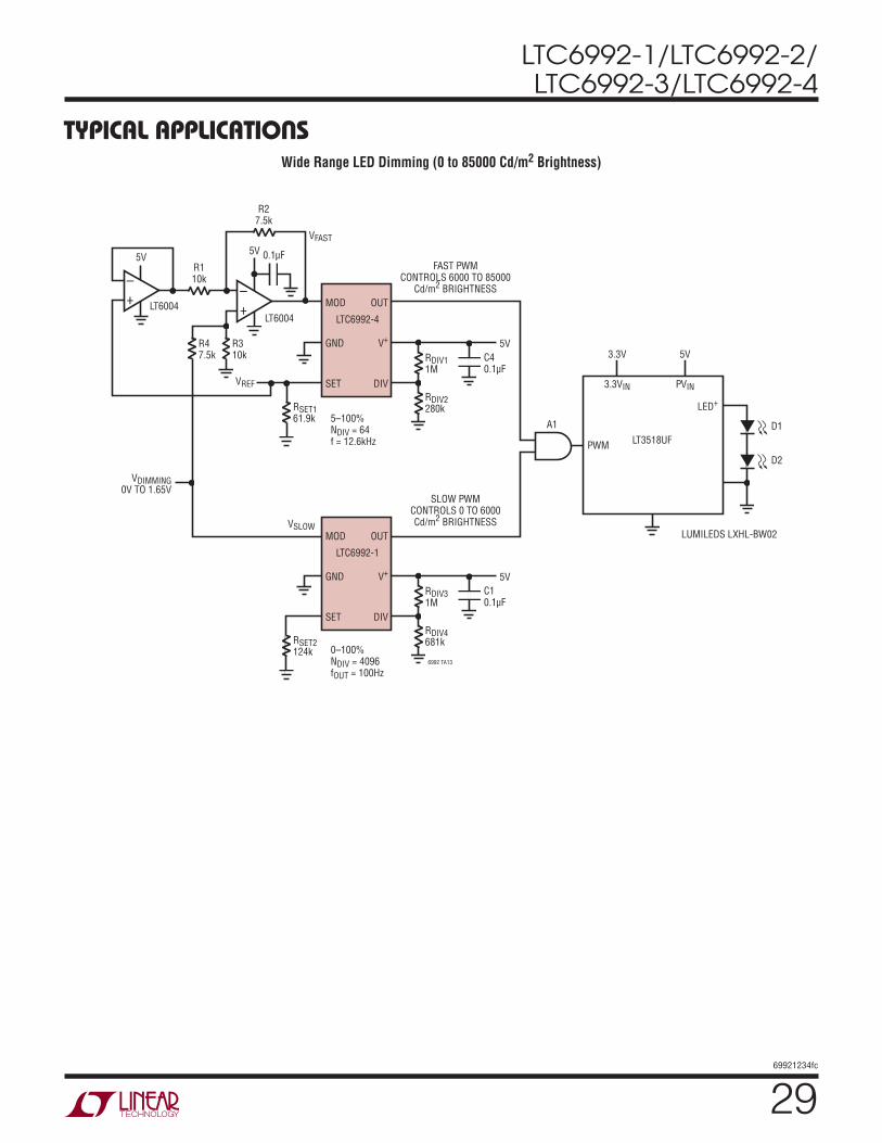
Typical applicaTionsWide Range LED Dimming (0 to 85000 Cd/m2 Brightness)
6992 TA13
LTC6992-4
MOD
GND
SET
OUT
V+
DIV
RDIV11M
RDIV2280k
5V
5V
LT6004
RSET161.9k
+–
5V
LT6004+–
R310k
VREF
VFAST
R47.5k
VDIMMING0V TO 1.65V
VSLOW
R27.5k
R110k
5–100%NDIV = 64f = 12.6kHz
0–100%NDIV = 4096fOUT = 100Hz
SLOW PWMCONTROLS 0 TO 6000Cd/m2 BRIGHTNESS
FAST PWMCONTROLS 6000 TO 85000
Cd/m2 BRIGHTNESS
C40.1µF
LTC6992-1
MOD
GND
SET
OUT
V+
DIV
RDIV31M
RDIV4681k
5V
3.3V 5V
RSET2124k
C10.1µF
3.3VIN PVIN
PWM
A1 D1
D2
LUMILEDS LXHL-BW02
LT3518UF
LED+
0.1µF
LTC6992-1/LTC6992-2/LTC6992-3/LTC6992-4
3069921234fc
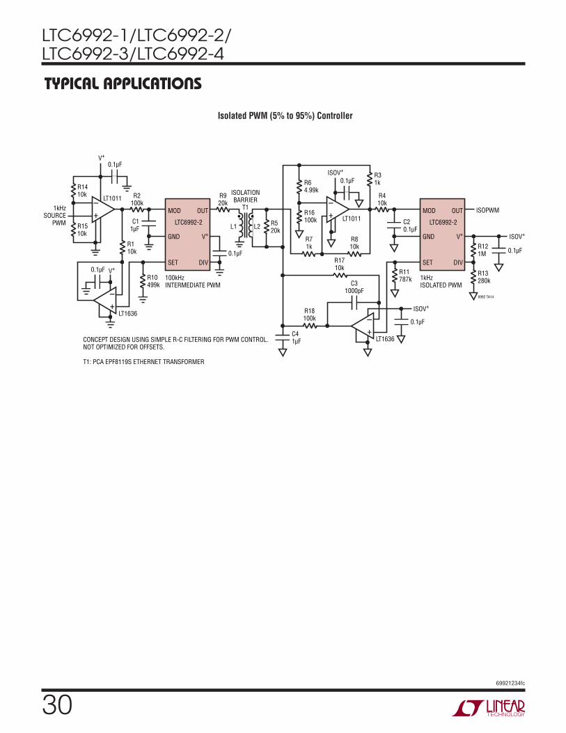
Isolated PWM (5% to 95%) Controller
6992 TA14
LTC6992-2
MOD
GND
SET
OUT
V+
DIV
LT1011
LT1636
CONCEPT DESIGN USING SIMPLE R-C FILTERING FOR PWM CONTROL.NOT OPTIMIZED FOR OFFSETS.
T1: PCA EPF8119S ETHERNET TRANSFORMER
R2100k
V+
R10499k
+–
R1510k
1kHzSOURCE
PWM
R1410k
R110k
100kHzINTERMEDIATE PWM
R920k
L1
+–
C11µF
0.1µF
L2LTC6992-2
MOD
GND
SET
OUT
V+
DIV
LT1011
LT1636
R410k
ISOV+
ISOV+
ISOV+
R11787k
R121M
ISOPWM
R13280k
R31k
+–
R64.99k
1kHzISOLATED PWM
ISOLATIONBARRIER
T1
R810k
C31000pF
R71k
+–
C20.1µF
R1710k
R18100k
R16100k••
V+
R520k
C41µF
0.1µF
0.1µF
0.1µF
0.1µF
0.1µF
Typical applicaTions

LTC6992-1/LTC6992-2/LTC6992-3/LTC6992-4
3169921234fc
DCB Package6-Lead Plastic DFN (2mm × 3mm)
(Reference LTC DWG # 05-08-1715 Rev A)
package DescripTion
3.00 ±0.10(2 SIDES)
2.00 ±0.10(2 SIDES)
NOTE:1. DRAWING TO BE MADE A JEDEC PACKAGE OUTLINE M0-229 VARIATION OF (TBD)2. DRAWING NOT TO SCALE3. ALL DIMENSIONS ARE IN MILLIMETERS4. DIMENSIONS OF EXPOSED PAD ON BOTTOM OF PACKAGE DO NOT INCLUDE MOLD FLASH. MOLD FLASH, IF PRESENT, SHALL NOT EXCEED 0.15mm ON ANY SIDE5. EXPOSED PAD SHALL BE SOLDER PLATED 6. SHADED AREA IS ONLY A REFERENCE FOR PIN 1 LOCATION ON THE
TOP AND BOTTOM OF PACKAGE
0.40 ± 0.10
BOTTOM VIEW—EXPOSED PAD
1.65 ± 0.10(2 SIDES)
0.75 ±0.05
R = 0.115TYP
R = 0.05TYP
1.35 ±0.10(2 SIDES)
13
64
PIN 1 BARTOP MARK
(SEE NOTE 6)
0.200 REF
0.00 – 0.05
(DCB6) DFN 0405
0.25 ± 0.050.50 BSC
PIN 1 NOTCHR0.20 OR 0.25 × 45° CHAMFER
0.25 ± 0.05
1.35 ±0.05(2 SIDES)
RECOMMENDED SOLDER PAD PITCH AND DIMENSIONS
1.65 ±0.05(2 SIDES)
2.15 ±0.05
0.70 ±0.05
3.55 ±0.05
PACKAGEOUTLINE
0.50 BSC
Please refer to http://www.linear.com/designtools/packaging/ for the most recent package drawings.

LTC6992-1/LTC6992-2/LTC6992-3/LTC6992-4
3269921234fc
S6 Package6-Lead Plastic TSOT-23
(Reference LTC DWG # 05-08-1636 Rev B)
1.50 – 1.75(NOTE 4)
2.80 BSC
0.30 – 0.45 6 PLCS (NOTE 3)
DATUM ‘A’
0.09 – 0.20(NOTE 3) S6 TSOT-23 0302 REV B
2.90 BSC(NOTE 4)
0.95 BSC
1.90 BSC
0.80 – 0.90
1.00 MAX0.01 – 0.10
0.20 BSC
0.30 – 0.50 REF
PIN ONE ID
NOTE:1. DIMENSIONS ARE IN MILLIMETERS2. DRAWING NOT TO SCALE3. DIMENSIONS ARE INCLUSIVE OF PLATING4. DIMENSIONS ARE EXCLUSIVE OF MOLD FLASH AND METAL BURR5. MOLD FLASH SHALL NOT EXCEED 0.254mm6. JEDEC PACKAGE REFERENCE IS MO-193
3.85 MAX
0.62MAX
0.95REF
RECOMMENDED SOLDER PAD LAYOUTPER IPC CALCULATOR
1.4 MIN2.62 REF
1.22 REF
package DescripTionPlease refer to http://www.linear.com/designtools/packaging/ for the most recent package drawings.

LTC6992-1/LTC6992-2/LTC6992-3/LTC6992-4
3369921234fc
Information furnished by Linear Technology Corporation is believed to be accurate and reliable. However, no responsibility is assumed for its use. Linear Technology Corporation makes no representa-tion that the interconnection of its circuits as described herein will not infringe on existing patent rights.
revision hisToryREV DATE DESCRIPTION PAGE NUMBER
A 01/11 Revised θJA value for TSOT package in the Pin Configuration.Added Note 7 for VOH and VOL in the Electrical Characteristics table.Minor edit to the Block Diagram.Minor edit to the equation in the “Duty Cycle Sensitivity to ∆VSET” section.Revised Typical Applications drawings.
24
121925
B 07/11 Revised Description and Order Information sectionsAdded additional information to ∆fOUT/∆V+ and included Note 11 in Electrical Characteristics sectionAdded Typical Frequency Error vs Time curve to Typical Performance Characteristics sectionAdded text to Basic Operation paragraph in Applications Information sectionCorrected fOUT value in Typical Applications drawing 6692 TA13
1 to 33, 4111929
C 01/12 Added MP-Grade 1, 2, 3, 5
LTC6992-1/LTC6992-2/LTC6992-3/LTC6992-4
3469921234fc
Linear Technology Corporation1630 McCarthy Blvd., Milpitas, CA 95035-7417 (408) 432-1900 FAX: (408) 434-0507 www.linear.com LINEAR TECHNOLOGY CORPORATION 2010
LT 0112 REV C • PRINTED IN USA
relaTeD parTs
Typical applicaTion
PART NUMBER DESCRIPTION COMMENTS
LTC1799 1MHz to 33MHz ThinSOT Silicon Oscillator Wide Frequency Range
LTC6900 1MHz to 20MHz ThinSOT Silicon Oscillator Low Power, Wide Frequency Range
LTC6906/LTC6907 10kHz to 1MHz or 40kHz ThinSOT Silicon Oscillator Micropower, ISUPPLY = 35µA at 400kHz
LTC6930 Fixed Frequency Oscillator, 32.768kHz to 8.192MHz 0.09% Accuracy, 110µs Start-Up Time, 105µA at 32kHz
LTC6990 TimerBlox, Voltage Controlled Oscillator Frequency from 488Hz to 1MHz, No Caps, 2.2% Accurate
LTC6991 TimerBlox, Very Low Frequency Clock with Reset Cycle Time from 2ms to 9.5 Hours, No Caps, 2.2% Accurate
LTC6993 TimerBlox, Monostable Pulse Generator Resistor Set Pulse Width from 1µs to 34sec, No Caps, 3% Accurate
LTC6994 TimerBlox, Delay Block/Debouncer Resistor Set Delay from 1µs to 34sec, No Caps Required, 3% Accurate
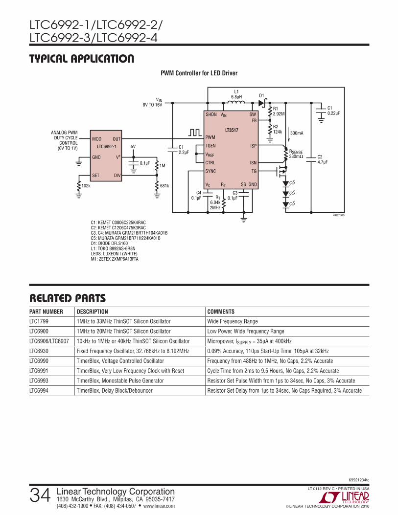
PWM Controller for LED Driver
6992 TA15
LTC6992-1
MOD
GND
SET
OUT
V+
DIV
1M
681k102k
VIN8V TO 16V
ANALOG PWMDUTY CYCLE
CONTROL(0V TO 1V) 5V
LT3517
PWM
TGEN
VREF
CTRL
SYNC
FB
ISP
ISN
TG
SHDN VIN SW
VC GNDSSRT
C12.2µF
0.1µF
R13.92M
R2124k 300mA
C10.22µF
C24.7µF
C30.1µF
C40.1µF RT
6.04k2MHz
D1L1
6.8µH
LT3517
RSENSE330mΩ
C1: KEMET C0806C225K4RACC2: KEMET C1206C475K3RACC3, C4: MURATA GRM21BR71H104KA01BC5: MURATA GRM21BR71H224KA01BD1: DIODE DFLS160L1: TOKO B992AS-6R8NLEDS: LUXEON I (WHITE)M1: ZETEX ZXMP6A13FTA