ltc3256 – wide vin range dual output 350ma step-down
TRANSCRIPT
LTC3256
13256fb
For more information www.linear.com/LTC3256
Typical applicaTion
FeaTures DescripTion
Wide VIN Range Dual Output 350mA Step-Down
Charge Pump with Watchdog Timer
The LTC®3256 is a wide input range switched capacitor step-down DC/DC converter that produces two regulated outputs: a 5V output via direct connection to the charge pump output, and a 3.3V output via a low dropout (LDO) linear post-regulator. The device provides up to 350mA of total output current. At 12V VIN and maximum load on both outputs, power dissipation is reduced by over 2W compared to a dual LDO regulator solution.
The LTC3256 maximizes efficiency by running the charge pump in 2:1 mode over as wide an operating range as pos-sible, and automatically switches to 1:1 mode as needed due to VIN and load conditions. Controlled input current and switching slew rates minimize conducted and radiated EMI. An integrated watchdog timer, independent power good outputs and reset input ensure reliable system operation and fault monitoring. A buffered 1.1V reference output enables system self-testing for safety critical applications.
The LTC3256 has numerous safety features including overcurrent fault protection, overtemperature protection and tolerance of 38V input transients. The LTC3256 is available in a thermally enhanced 16-lead MSOP plastic package with exposed pad (MSE16).
High Efficiency Dual Output Power Supply Power Dissipation vs Input Voltage
applicaTions
n Input Voltage Range: 5.5V to 38V n Independently Enabled 5V and 3.3V Fixed Outputs n 5V Output: 100mA Max n 3.3V LDO Output: 250mA Max n Multimode Step-Down Charge Pump (2:1, 1:1) with
Automatic Mode Switching n Low Quiescent Current
n 20μA with Both Outputs Regulating (No Load) n 0.5μA in Shutdown
n Engineered for Diagnostic Coverage in ISO26262 Systems
n 1.1V Reference Output for System Diagnostics n Power-On Reset and Watchdog Controller with
Adjustable Timing n Overcurrent Fault Protection on Each Output n Overtemperature Protection n 150°C Max Operating Junction Temperature n Thermally Enhanced 16-Lead MSOP Package
n Automotive ECU/CAN Transceiver Supplies n Industrial/Telecom Housekeeping Supplies n Low Power 12V to 5V and 3.3V Conversion L, LT, LTC, LTM, Linear Technology and the Linear logo are registered trademarks and
ThinSOT is a trademark of Linear Technology Corporation. All other trademarks are the property of their respective owners.
10µF
10µF
10µF
10µF1M
3256 TA01
MICROCONTROLLERINTERFACE
5V OUTPUT100mA MAX
3.3V LDO OUTPUT250mA MAX
5.5V TO 38VINPUT SUPPLY
OUTCP
OUT5
OUT3
PG3PG5
RSTI
REFOUT
RSTWDI
VIN
EN5EN3
RTWT
GND
LTC3256
1µF
C+ C–
0.1µF3256 TA01a
6 7 8 9 10 11 12 13 14 15 16
INPUT VOLTAGE (V)
0.0
0.5
1.0
1.5
2.0
2.5
3.0
3.5
4.0
4.5
5.0
POW
ER D
ISSI
PATI
ON (W
)
3.3V LOAD = 250mA5V LOAD = 100mA
LTC3256
IDEAL DUAL LDO

LTC3256
23256fb
For more information www.linear.com/LTC3256
pin conFiguraTionabsoluTe MaxiMuM raTings
VIN, EN3, EN5, WDI .................................... –0.3V to 38VOUTCP, OUT3, OUT5 ................................. –0.3V to 5.5VOUT3, OUT5 Short Circuit Duration ................. IndefinitePG3, PG5, REFOUT ............................... –0.3V to VOUTCPRST ........................................................... –0.3V to 5.5VWT, RT .................................................. –0.3V to VOUTCPRSTI ......................................................... –0.3V to 5.5VOperating Junction Temperature Range (Notes 3, 4) LTC3256E .......................................... –40°C to 125°C LTC3256I ........................................... –40°C to 125°C LTC3256H .......................................... –40°C to 150°C LTC3256MP ....................................... –55°C to 150°CStorage Temperature Range .................. –65°C to 150°CLead Temperature (Soldering, 10 sec) ................... 300°C
(Notes 1, 2)
12345678
C–
C+
OUTCPOUT5
REFOUTOUT3
PG3PG5
161514131211109
EN5EN3VINWDIRSTIRTWTRST
TOP VIEW
MS PACKAGE16-LEAD PLASTIC MSOP
17GND
TJMAX = 150°C, θJC = 10°C/W
θJA = 40°C/W EXPOSED PAD (PIN 17) IS GND, MUST BE SOLDERED TO PCB
orDer inForMaTionLEAD FREE FINISH TAPE AND REEL PART MARKING* PACKAGE DESCRIPTION TEMPERATURE RANGE
LTC3256EMSE#PBF LTC3256EMSE#TRPBF 3256 16-Lead Plastic MSOP –40°C to 125°C
LTC3256IMSE#PBF LTC3256IMSE#TRPBF 3256 16-Lead Plastic MSOP –40°C to 125°C
LTC3256HMSE#PBF LTC3256HMSE#TRPBF 3256 16-Lead Plastic MSOP –40°C to 150°C
LTC3256MPMSE#PBF LTC3256MPMSE#TRPBF 3256 16-Lead Plastic MSOP –55°C to 150°C
Consult LTC Marketing for parts specified with wider operating temperature ranges. *The temperature grade is identified by a label on the shipping container.For more information on lead free part marking, go to: http://www.linear.com/leadfree/ For more information on tape and reel specifications, go to: http://www.linear.com/tapeandreel/. Some packages are available in 500 unit reels through designated sales channels with #TRMPBF suffix.
http://www.linear.com/product/LTC3256#orderinfo

LTC3256
33256fb
For more information www.linear.com/LTC3256
elecTrical characTerisTics
SYMBOL PARAMETER CONDITIONS MIN TYP MAX UNITS
VIN Operating Input Voltage Range (Note 5) l 5.5 38 V
VIN Undervoltage Lockout Threshold l 1.8 2.7 V
VIN Quiescent Current EN5 = EN3 = 0V Only One Output Enabled Both OUT3 and OUT5 Enabled
Shutdown Output In Regulation, No Load Output In Regulation, No Load
0.5 15 20
2
30 35
µA µA µA
EN3, EN5 Input High Voltage 1.2 2 V
EN3, EN5 Input Low Voltage 0.4 0.9 V
EN3, EN5 Input Low Current VPIN = 0V –1 0 1 µA
EN3, EN5 Input High Current VPIN = 38V 1 3 µA
Charge Pump Operation
VOUTCP OUTCP Regulation Voltage EN3 and/or EN5 High 5.05 V
OUTCP Short Circuit Current VOUTCP = GND 600 mA
Charge Pump Output Impedance 2:1 Step-Down Mode 1:1 Step-Down Mode, VIN = 5.5V
2 2
Ω Ω
5V Output Operation
VOUT5 Fixed 5V Output Regulation (Note 5) EN5 High, VIN = 5.5V, IOUT ≤ 100mA EN5 High, VIN = 12V, IOUT ≤ 100mA EN5 High, VIN = 38V, IOUT = 0mA
l
l
l
4.85 4.85 4.85
5.05 5.05 5.05
5.19 5.19 5.19
V V V
OUTCP to OUT5 Power Switch On-Resistance
EN5 High 0.6 Ω
OUT5 Overvoltage Threshold VOUT5 Rising Makes PG5 Go Low VOUT5 Falling Makes PG5 Go Hi-Z
l 5.25 5.1
5.4 V V
OUT5 Undervoltage Threshold VOUT5 Rising Makes PG5 go Hi-Z VOUT5 Falling Makes PG5 go Low
l
4.6
4.9 4.75
V V
PG5 Output Low Voltage IPG5 = 100µA l 0.1 0.4 V
PG5 Output Hi-Z Leakage VPG5 = 5V l –1 0 1 µA
3.3V LDO Operation
VOUT3 Fixed 3.3V LDO Output Regulation (Note 5) EN3 High, VIN = 5.5V, IOUT ≤ 250mA EN3 High, VIN = 12V, IOUT ≤ 250mA EN3 High, VIN = 38V, IOUT = 0mA
l
l
l
3.170 3.200 3.234
3.30 3.30 3.30
3.366 3.366 3.366
V V V
OUT3 Overvoltage Threshold VOUT3 Rising Makes PG3 Go Low VOUT3 Falling Makes PG3 Go Hi-Z
l 3.465 3.35
3.58 V V
OUT3 Undervoltage Threshold VOUT3 Rising Makes PG3 Go Hi-Z VOUT3 Falling Makes PG3 Go Low
l
3.04
3.24 3.135
V V
PG3 Output Low Voltage IPG3 = 100µA l 0.1 0.4 V
PG3 Output Hi-Z Leakage VPG3 = 5V l –1 0 1 µA
Buffered 1.1V Reference Output (REFOUT)
REFOUT Pin Output Voltage EN3 and/or EN5 High, IREFOUT = 0mA l 1.068 1.1 1.132 V
REFOUT Pin Output Resistance 2 4 kΩ
Reset Timer Control (RT)
External Timer RT Pull-Up Current VRT = 0.3V l –1.1 –1.9 –2.6 µA
External Timer RT Pull-Down Current VRT = 1.3V l 1.1 1.9 2.6 µA
Internal Timer RT Pull Down Current VRT = VOUTCP l 0.25 1 µA
RT Internal Timer Select Threshold l 1.8 2.3 2.7 V
The l denotes the specifications which apply over the specified operating junction temperature range, otherwise specifications are at TA = 25°C (Note 3). VIN = 12V, CFLY = 1µF unless otherwise noted.

LTC3256
43256fb
For more information www.linear.com/LTC3256
SYMBOL PARAMETER CONDITIONS MIN TYP MAX UNITS
Reset Timer Input (RSTI)
RSTI Input High Voltage l 1.2 1.26 V
RSTI Input Low Voltage l 1.1 1.16 V
RSTI Input Low Current VRST_IN = 0V l –1 0 1 µA
RSTI Input High Current VRST_IN = 5V l –1 0 1 µA
Reset Output (RST)
tRST(INT) Internal Reset Timeout Period VRT = VOUTCP l 150 200 260 ms
tRST(EXT) External Reset Timeout Period CRT = 2.2nF l 26 32 44 ms
tUV RSTI Low to RST Asserted From RSTI falling to 1V or less l 10 80 150 µs
RST Output Voltage Low VOUTCP = 5V, IRST = 100µA l 0.1 0.4 V
RST Output Voltage High Leakage RST = 5V l –1 0 1 µA
Watchdog Timer Control (WT)
External Timer WT Pull-Up Current VWT = 0.3V l –1.1 –1.9 –2.6 μA
External Timer WT Pull-Down Current VWT = 1.3V l 1.1 1.9 2.6 μA
Internal Timer WT Detect Pull Down Current VWT = VOUTCP l 0.25 1 μA
WT Internal Timer Select Threshold l 1.8 2.3 2.7 V
Watchdog Input (WDI)
tWDU(INT) Internal Watchdog Upper Boundary VWT = VOUTCP l 1.3 1.6 2 s
tWDL(INT) Internal Watchdog Lower Boundary VWT = VOUTCP l 37.5 50 62.5 ms
tWDR(EXT) External Watchdog Reset Time CWT = 2.2nF l 200 260 340 ms
tWDU(EXT) External Watchdog Upper Boundary tWDR(EXT) • (128/129) ms
tWDL(EXT) External Watchdog Lower Boundary tWDR(EXT) • (5/129) ms
WDI Input High Voltage 1.2 2 V
WDI Input Low Voltage 0.4 0.9 V
WDI Input Low Current VWD_IN = 0V –1 0 1 µA
WDI Input High Current VWD_IN = 5V –1 0 1 µA
Input Pulsewidth l 100 ns
elecTrical characTerisTics The l denotes the specifications which apply over the specified operating junction temperature range, otherwise specifications are at TA = 25°C (Note 3). VIN = 12V, CFLY = 1µF unless otherwise noted.
Note 1: Stresses beyond those listed under Absolute Maximum Ratings may cause permanent damage to the device. Exposure to any Absolute Maximum Rating condition for extended periods may affect device reliability and lifetime.Note 2: All voltages are referenced to GND unless otherwise specified.Note 3: The LTC3256E is guaranteed to meet performance specifications from 0°C to 85°C operating junction temperature. Specifications over the –40°C to 125°C operating junction temperature range are assured by design, characterization and correlation with statistical process controls. The LTC3256I is guaranteed over the –40°C to 125°C operating junction temperature range. The LTC3256H is guaranteed over the –40°C to 150°C operating junction temperature range. The LTC3256MP is guaranteed and tested over the –55°C to 150°C operating junction temperature range. High junction temperatures degrade operating lifetimes; operating lifetime is derated for junction temperatures greater than 125°C. Note that the maximum ambient temperature consistent with these specifications is determined by specific operating conditions in conjunction with board layout, the rated package thermal resistance and other environmental factors.
The junction temperature (TJ, in °C) is calculated from the ambient temperature (TA, in °C) and power dissipation (PD, in Watts) according to the formula: TJ = TA + (PD • θJA)where θJA (in °C/W) is the package thermal impedance.Note 4: This IC has overtemperature protection that is intended to protect the device during momentary overload conditions. Junction temperatures will exceed 150°C when overtemperature protection is active. Continuous operation above the specified maximum operating junction temperature may impair device reliability.Note 5: The maximum operating junction temperature of 150°C must be followed. Certain combinations of input voltage and output current will cause the junction temperature to exceed 150°C and must be avoided. See Thermal Management section for information on calculating maximum operating conditions. Due to thermal limitations of production equipment, only no load regulation is checked at 38V.

LTC3256
53256fb
For more information www.linear.com/LTC3256
Typical perForMance characTerisTics
3.3V Output Voltage vs Input Voltage at 25mA
3.3V Output Voltage vs Input Voltage at 250mA Output Voltages vs Input Voltage
5V Output Voltage vs Input Voltage at 10mA
5V Output Voltagevs Input Voltage at 100mA
Efficiency and Power Lossvs Input Voltage
Input Operating Current vs Input Voltage
No Load Input Current vs Input Voltage
Input Shutdown Current vs Input Voltage
TA = 25°C, unless otherwise noted.
0 4 8 12 16 20 24 28 32 36 40
IN V (V)
0
1
2
3
4
5
6
7
8
9
10
IN
I(µ
A)
3256 G01
125°C85°C25°C–55°C
0 5 10 15 20 25 30 35 40
IN V (V)
0
10
20
30
40
50
IN
I(µ
A)
3256 G02
EN3 HIGHEN5 HIGHBOTH HIGH
5 6 7 8 9 10 11 12 13 14 15
IN V (V)
0
10
20
30
40
50
IN
I(µ
A)
3256 G03
EN3=EN5=HIGH
150°C25°C–55°C
0 5 10 15 20 25 30 35 40
IN V (V)
3.15
3.20
3.25
3.30
3.35
3.40
3.45
V O
UT3
(V)
3256 G04
OUT3 I =25mA
150°C25°C–55°C
5 6 7 8 9 10 11 12 13 14 15
IN V (V)
3.15
3.20
3.25
3.30
3.35
3.40
3.45
3256 G05
OUT3 I =250mA 125°C25°C–55°C
V OUT
3 (V
)
5 6 7 8 9 10 11 12 13 14 15
IN V (V)
2.5
3.0
3.5
4.0
4.5
5.0
5.5
OUT
V(V
)
3256 G06
No Load
VOUT3
VOUT5
VOUTCP
0 5 10 15 20 25 30 35 40
IN V (V)
4.80
4.85
4.90
4.95
5.00
5.05
5.10
5.15
5.20
3256 G07
OUT5 I =10mA
150°C25°C–55°C
V OUT
5 (V
)
5 6 7 8 9 10 11 12 13 14 15
IN V (V)
4.80
4.85
4.90
4.95
5.00
5.05
5.10
5.15
5.20
3256 G08
OUT5 I =100mA 125°C25°C–55°C
V OUT
5 (V
)
5 6 7 8 9 10 11 12 13 14 15
IN V (V)
0
10
20
30
40
50
60
70
80
90
EFFI
CIEN
CY (%
)
3256 G09
EFFICIENCY
LOSS
OUT3 I =250mAOUT5 I =100mA
0.0
0.5
1.0
1.5
2.0
2.5
3.0
3.5
4.0
4.5
POWER LOSS (W
)

LTC3256
63256fb
For more information www.linear.com/LTC3256
Typical perForMance characTerisTics
Reset Timeout Period vs RT Capacitance
Watchdog Timeout Period vs WT Capacitance RSTI Threshold vs Temperature
REFOUT Voltage vs Input VoltageInternal Reset Timeout Period vs Temperature
Internal Watchdog Timeout Period vs Temperature
TA = 25°C, unless otherwise noted.
0 5 10 15 20 25 30 35 40
IN V (V)
1.06
1.07
1.08
1.09
1.10
1.11
1.12
1.13
1.14
REFO
UT
V(V
)
3256 G10
150°C25°C–55°C
−60 −30 0 30 60 90 120 150
TEMPERATURE (°C)
0.10
0.15
0.20
0.25
0.30
TIM
E (S
EC)
3256 G11
−60 −30 0 30 60 90 120
TEMPERATURE (°C)
1.2
1.3
1.4
1.5
1.6
1.7
1.8
TIM
E (S
EC)
3256 G12
RT PIN CAPACITANCE, CRT (nF)0.001 0.01 0.1 1 10 100 1k
0.1
1
10
100
1k
10k
50k
RESE
T TI
MEO
UT P
ERIO
D, T
RST(
EXT)
(ms)
3256 G13WT PIN CAPACITANCE, CWT (nF)
0.001 0.01 0.1 1 10 100 1k1
10
100
1k
10k
100k
500k
WAT
CHDO
G TI
MEO
UT P
ERIO
D, T
WDR
(EXT
) (m
s)
3256 G14
RISINGFALLING
TEMPERATURE (°C)–60 –30 0 30 60 90 120 150
1.130
1.150
1.170
1.190
1.210
1.230
RSTI
THR
ESHO
LD (V
)
3256 G15

LTC3256
73256fb
For more information www.linear.com/LTC3256
TA = 25°C, unless otherwise noted.Typical perForMance characTerisTics
OUT3 Power-Up OUT3 Power-Up OUT3 Transient Response
OUT5 Power-Up OUT5 Power-Up OUT5 Transient Response
Output Ripple Output Ripple Output Ripple
25µs/DIV
OUTCPAC 0.1V/DIV
OUT5AC 0.1V/DIV
OUT3AC 5mV/DIV
REFOUTAC 5mV/DIV
3256 G16
VIN = 12VIOUT5 = 100mAIOUT3 = 250mA
5µs/DIV
OUTCPAC 0.1V/DIV
OUT5AC 0.1V/DIV
OUT3AC 5mV/DIV
REFOUTAC 5mV/DIV
3256 G17
VIN = 12VIOUT5 = 20mAIOUT3 = 100mA
5µs/DIV
OUTCPAC 0.1V/DIV
OUT5AC 0.1V/DIV
OUT3AC 5mV/DIV
REFOUTAC 5mV/DIV
3256 G17
VIN = 5.5VOUT5 = 20mAIOUT3 = 100mA
100µs/DIV
EN31
0
OUTCPDC 5V/DIV
OUT3DC 1V/DIV
PG3
3256 G19
VIN = 12VROUT3 = 33Ω
100µs/DIV
EN31
0
OUTCPDC 5V/DIV
OUT3DC 1V/DIV
PG3
3256 G20
VIN = 5.5VROUT3 = 33Ω
100µs/DIV
OUTCPAC 0.1V/DIV
OUT3AC 20mV/DIV
IOUT3
250mA
20mA3256 G21
VIN = 12V
500µs/DIV
OUTCPDC 5V/DIV
OUT5DC 2V/DIV
1
0
PG5
EN5
3256 G22
VIN = 12VROUT5 = 100Ω
100µs/DIV
OUTCPDC 5V/DIV
OUT5DC 2V/DIV
1
0
PG5
EN5
3256 G23
VIN = 5.5VROUT5 = 100Ω
100µs/DIV
OUT5AC 50mV/DIV
VIN=12V
OUT5AC 50mV/DIV
VIN=5.5V
100mA
10mAIOUT5
3256 G24

LTC3256
83256fb
For more information www.linear.com/LTC3256
pin FuncTionsC– (Pin 1): Charge Pump Flying Capacitor Negative Con-nection.
C+ (Pin 2): Charge Pump Flying Capacitor Positive Con-nection.
OUTCP (Pin 3): Charge Pump Output. The charge pump output should be bypassed with a 10µF or greater X7R ceramic capacitor. The charge pump output is enabled if either ENx pin is logic high. OUTCP is the input supply for the 3.3V LDO.
OUT5 (Pin 4): 5V Output Pin. Connects to the charge pump output, OUTCP, through an internal power switch controlled by the EN5 input when VIN > 10V (typical), and regulates to 5V with VIN as a power source when VIN < 10V (typical).
REFOUT (Pin 5): 1.1V Reference Output. Provides a buff-ered version of the LTC3256’s internal bandgap reference voltage with 2k output impedance (typical). To maximize supply rejection, REFOUT should be bypassed with a 0.1µF ceramic capacitor.
OUT3 (Pin 6): 3.3V Low-Dropout Linear Regulator (LDO) Output Pin. The charge pump output, OUTCP, serves as the 3.3V LDO’s input supply.
PG3 (Pin 7): Power Good Open Drain Logic Output. Goes high impedance when OUT3 is near its final operating volt-age. PG3 is intended to be pulled up to a low voltage supply (such as OUT3, OUT5 or OUTCP) with an external resistor.
PG5 (Pin 8): Power Good Open Drain Logic Output. Goes high impedance when OUT5 is near its final operating volt-age. PG5 is intended to be pulled up to a low voltage supply (such as OUT3, OUT5 or OUTCP) with an external resistor.
RST (Pin 9): Reset Open Drain Logic Output. The RST pin is low impedance to GND during the reset period, and goes high impedance during the watchdog period. RST is intended to be pulled up to low voltage supply (such as OUT3, OUT5, or OUTCP) with an external resistor.
WT (Pin 10): Watchdog Timer Control Pin. Attach an external capacitor (CWT) to GND to set the watchdog upper boundary timeout. Tie WT to OUTCP to generate a timeout of about 1.6s. Tie WT and WDI to GND to disable the watchdog timer.
RT (Pin 11): Reset Timeout Control Pin. Attach an external capacitor (CRT) to GND to set the reset timeout period, RT can be left open to minimize the reset timeout. Tie RT to OUTCP to generate a reset timeout of about 200ms.
RSTI (Pin 12): Reset Logic Comparator Input Pin. The RSTI input is compared to a 1.2V (typical) threshold voltage. If RSTI is below the threshold voltage the LTC3256 will enter the reset state and drive the RST pin low. Once RSTI rises above the threshold voltage, the reset timer is started and the RST pin is held low until the reset period times out.
WDI (Pin 13): Watchdog Logic Input Pin. Application circuitry must toggle the logic state of this pin such that falling edges occur at a rate faster than the watchdog up-per boundary time but slower than the watchdog lower boundary time. If these conditions are not met, RST will be asserted low. Tie WT and WDI to GND to disable the watchdog timer. Do not float this pin.
VIN (Pin 14): Power Input Pin. Input voltage for both charge pump and IC control circuitry.
EN3 (Pin 15): Logic input pin which enables the 3.3V LDO when high and disables it when low. Bringing EN3 high causes the charge pump to enable if it isn’t already on. The LDO powers up once the charge pump output, OUTCP, rises above 97.5% of its regulation value (typical). The EN3 pin has a 1μA (typical) pull down current to ground and can tolerate 38V inputs.
EN5 (Pin 16): Logic Input Pin. Enables or disables the 5V output, OUT5. Bringing EN5 high causes the charge pump to enable if it isn’t already on. When the charge pump output rises above 97.5% of its regulation value (typical), a fault protected internal power switch connects OUTCP to OUT5, delivering power to any OUT5 load. A soft-start circuit limits any inrush current through the switch to help avoid glitching the charge pump output. If the input voltage falls below 10V (typical) and the charge pump regulates to a voltage lower than 5V, OUT5 receives its power directly from a VIN-powered 1:1 mode regulator. The EN5 pin has a 1μA (typical) pull down current to ground and can tolerate 38V inputs.
GND (Exposed Pad): Ground. The exposed package pad is ground and must be soldered to the PC board ground plane for proper functionality and for rated thermal performance.
LTC3256
93256fb
For more information www.linear.com/LTC3256
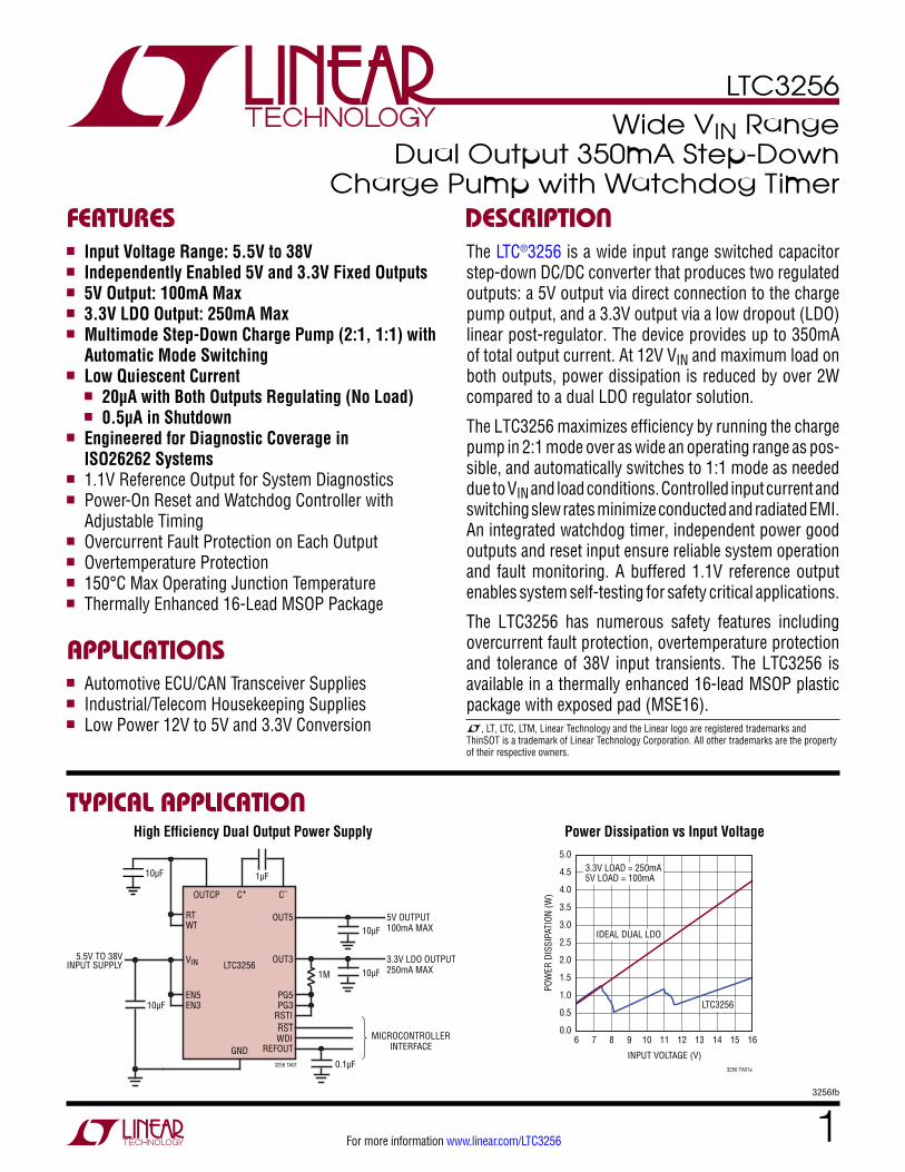
TiMing DiagraM
RSTI
RST
tUV tRST
3256 TD01
WDI
RST
tWDRtWDL < t < tWDUtRST
3256 TD02tRSTt < tWDL
Reset Timing
Watchdog Timing

LTC3256
103256fb
For more information www.linear.com/LTC3256
siMpliFieD block DiagraM
–+
–+
–+
–+
–+
–+
–+
–+
–+
VIN
EN5
EN3
REFOUT
RST
RT
OUT5 GND3256 BD
PG5
PG3
OUT3
OUTCP
5.5V
5V 3.6V
5.05V
7.2V 10.1V 38V
1:1MODE
2:1MODE
2:1/1:1 MODE STEP-DOWN CHARGE PUMP
EXTERNALFLYING
CAPACITORCONNECTION
C–
C+
CLOCKOSCILLATOR
FALLINGEDGE
DETECTOR
WATCHDOGTIMER
OUT5 INPUTSELECTOR POWER GOOD
WINDOWCOMPARATORS
FAULT-PROTECTEDPMOS SWITCH
5V
3.3V
3.3V 250mA LDO
OUTCPGOOD
3.4V
WT
WDI
RSTI
1.1VBANDGAP
REFERENCE
2k
ENABLE LOGIC
OUT5 ON
OUT3 ON
OUTCP ON
1.2V
VIN
VIN-POWERED1:1 MODE
5V REGULATOR
VOUTCP
LTC3256
113256fb
For more information www.linear.com/LTC3256
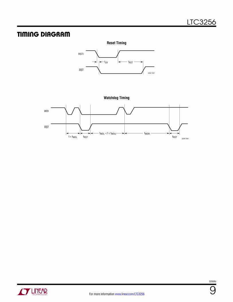
The LTC3256 is an inductorless wide input range step-down DC/DC converter that produces 5V and 3.3V regulated outputs with a total output current of 350mA. It uses a step-down charge pump with automatic 2:1/1:1 mode switching as a pre-regulator for the 5V and 3.3V outputs. This optimizes system efficiency and minimizes thermal problems due to excess power dissipation. In typical 12V automotive systems, the LTC3256 reduces power dissipation by a full 2W at maximum load relative to a dual LDO solution.
Each regulated output may be independently enabled to provide maximum flexibility. Enabling either of the regulator outputs will first turn on the step-down charge pump. Once the charge pump nears its regulation point, the enabled outputs will turn on in a controlled, soft-started manner. The 3.3V output is provided by an LDO that is always powered from the charge pump output. The 5V output is typically powered from the regulated charge pump via an overcurrent protected switch directly connected to the charge pump output.
The charge pump typically produces a regulated 5.05V output but allows this output to drop as needed in order to stay in 2:1 mode and maximize overall efficiency whenever VIN falls below ~10.1V. If VIN falls near the low end of its operating range, the charge pump automatically enters 1:1 mode as required to keep the 3.3V LDO in regulation. Whenever the charge pump output drops below 5V, the regulated 5V output will automatically be supplied using a simple gated switch regulator powered from VIN.
2:1 Step-Down Charge Pump Operation (VIN > ~10.1V)
The increased efficiency and reduced power dissipation advantages of the LTC3256 arise from the use of a 2:1 step-down charge pump to perform the bulk of the voltage step-down from VIN to 5V and 3.3V. An ideal 2:1 charge-pump has the property that its input current is exactly half its output current (See Figure 1). In real-world charge pumps like the LTC3256, input current slightly exceeds half the output current due to additional current needed for biasing and for driving power switches.
applicaTions inForMaTion
Figure 2 shows the power switch topology of the 2:1 step-down charge pump in the LTC3256. When operat-ing in 2:1 mode, the part employs a two phase clock to turn on only switches A and C in one phase followed by switches B and D only in the other phase. Current source IA controls the maximum output current that the part can deliver. When the charge pump clock is active, VOUTCP will increase towards VIN/2. Once VOUTCP reaches the appropriate regulation point, the charge pump shuts off all four switches and enters a SLEEP state to minimize quiescent current until the output voltage falls below its regulation point.
Figure 1. Steady-State Time-Averaged Current Flows in an Ideal 2:1 Charge Pump
IIN =ILOAD
2
IIN =ILOAD
2
ILOAD
2
ILOAD
VOUT
ILOAD
VIN
GND
INPUT
IDEAL 2:1 CHARGE PUMP
OUTPUT
3256 F01
+
–
LOAD+–
Figure 2. LTC3256 2:1 Step-Down Charge Pump Power Switch Topology
+– VIN
SWITCH A SWITCH B
SWITCH D SWITCH C
OUTCP
3256 F02
+
–
IA
VIN
COUTCP
VOUTCPGND
C+
C–
CFLY

LTC3256
123256fb
For more information www.linear.com/LTC3256
Under typical conditions (VIN > 10.1V), the LTC3256 operates in 2:1 mode and both the 5V output and 3.3V LDO are powered directly from the charge pump output (see Figure 3).
applicaTions inForMaTion
The overall efficiency and power dissipation under typical 2:1 step-down conditions can be approximated with the equations below.
Total LTC3256 efficiency when VIN > ~10.1V:
η≅ 5V •IOUT5 +3.3V •IOUT3
VIN •IOUT5
2+ IOUT3
2⎛⎝⎜
⎞⎠⎟
Total LTC3256 power dissipation when VIN > ~10.1V:
PD ≅ VIN
2– 5V⎛
⎝⎜⎞⎠⎟ •IOUT5 +
VIN2
– 3.3V⎛⎝⎜
⎞⎠⎟ •IOUT3
2:1 Step-Down Charge Pump Operation (~7.2V < VIN < ~10.1V)
In this operating region, the charge pump regulates slightly below VIN/2 in order to remain in 2:1 mode and maximize overall VIN to 3.3V conversion efficiency. Figure 4 shows typical charge pump step-down mode and output voltage as a function of VIN.
12V IN
PMOSSWITCH
OUTCP3256 F03
5.05V PREREGULATED OUTPUT FOREXTERNAL BYPASS CAPACITOR CONNECTION
OUT3
OUT5 5V OUT100mA MAX
3.3V OUT250mA MAX
VIN
3.3V LDO
CHARGE PUMPIN 2:1 MODE
350mAMAX OUTPUT
Figure 3. Power Connections for Typical 12V VIN Operation
If OUT5 is enabled and the charge pump output falls below 5V, OUT5 is disconnected from the charge pump output and a separate internal VIN-powered 1:1 step-down mode regulator is used to regulate 5V at the OUT5 pin. Refer to the Simplified Block Diagram. The 3.3V LDO remains powered by the 2:1 charge pump output.
Overall efficiency and power dissipation in this operating region can be approximated by the equations below.
Total LTC3256 efficiency when ~7.2V < VIN < ~10.1V:
η≅ 5V •IOUT5 +3.3V •IOUT3
VIN • IOUT5 +IOUT3
2⎛⎝⎜
⎞⎠⎟
Total LTC3256 power dissipation when ~7.2V < VIN < ~10.1V:
PD ≅ VIN – 5V( ) •IOUT5 +
VIN2
– 3.3V⎛⎝⎜
⎞⎠⎟ •IOUT3
Figure 4. Typical Charge Pump Output Voltage and Mode vs VIN
5.5V
3.6V
5.05V
7.2V 10.1V 38V
1:1MODE
2:1MODE
VIN
VOUTCP

LTC3256
133256fb
For more information www.linear.com/LTC3256
applicaTions inForMaTion1:1 Step-Down Charge Pump Operation (VIN < ~7.2V)
At the low end of the VIN operating range, the minimum charge pump regulation point is typically VOUTCP = 3.6V, with the charge pump automatically switching to 1:1 mode as needed to maintain regulation. Under 1:1 mode condi-tions, both the 5V and 3.3V outputs are powered directly from VIN with no improvement in efficiency over a dual LDO solution. The overall efficiency and power dissipa-tion in 1:1 step-down mode can be approximated by the equations below.
Total LTC3256 efficiency when VIN < ~7.2V:
η≅ 5V •IOUT5 +3.3V •IOUT3VIN • IOUT5 +IOUT3( )
Total LTC3256 power dissipation when VIN < ~7.2V: PD ≅ VIN – 5V( ) •IOUT5 + VIN – 3.3V( ) •IOUT3
Referring to Figure 2, in 1:1 mode, charge pump switches C and D remain off, and switches A and B are pulsed on and off together to transfer charge directly from VIN to OUTCP.
VIN Bypass Capacitor Selection
The total amount and type of capacitance necessary for input bypassing is very dependent on the impedance of the input power source as well as existing bypassing already on the VIN node. For optimal input noise and ripple reduction, it is recommended that a low ESR ceramic capacitor be used for VIN bypassing. Low ESR will reduce the voltage steps caused by changing input current, while the absolute capacitor value will determine the level of ripple. An electro-lytic or tantalum capacitor may be used in parallel with the ceramic capacitor on VIN to increase the total capacitance, but due to the higher ESR, it is not recommended that an electrolytic or tantalum capacitor be used alone for input bypassing. The LTC3256 will operate with capacitors less than 10μF, but depending on the source impedance, input noise can feed through to the output causing degraded performance. For best performance, 10μF or greater total capacitance is suggested for VIN bypassing.
Flying Capacitor Selection
The flying capacitor should always be a ceramic type. Polarized capacitors such as tantalum or aluminum electrolytics are not recommended. The flying capacitor controls the strength of the charge pump. In order to achieve the rated output current, it is necessary for the flying capacitor to have at least 0.4μF of capacitance over operating temperature at 5.05V (see Ceramic Capacitor Selection Guidelines). The voltage rating of the ceramic capacitor should be 6V or greater.
Ceramic Capacitor Selection Guidelines
Capacitors of different materials lose their capacitance with higher temperature and voltage at different rates. For example, a ceramic capacitor made of X5R or X7R material will retain most of its capacitance from –40°C to 85°C, whereas a Z5U or Y5V style capacitor will lose considerable capacitance over that range (60% to 80% loss typical). Z5U and Y5V capacitors may also have a very strong voltage coefficient, causing them to lose an additional 60% or more of their capacitance when the rated voltage is applied. Therefore, when comparing different capacitors, it is often more appropriate to compare the amount of achievable capacitance for a given case size rather than discussing the specified capacitance value. For example, over rated voltage and temperature conditions, a 4.7μF, 10V, Y5V ceramic capacitor in an 0805 case may not provide any more capacitance than a 1μF, 10V, X5R or X7R available in the same 0805 case. In fact, over bias and temperature range, the 1μF, 10V, X5R or X7R will provide more capacitance than the 4.7μF, 10V, Y5V. The capacitor manufacturer’s data sheet should be consulted to determine what value of capacitor is needed to ensure minimum capacitance values are met over operating temperature and bias voltage. Table 1 is a list of ceramic capacitor manufacturers in alphabetical order:

LTC3256
143256fb
For more information www.linear.com/LTC3256
applicaTions inForMaTionTable 1CERAMIC CAPACITOR MANUFACTURER WEBSITE
AVX www.avxcorp.com
Kemet www.kemet.com
Murata www.murata.com
Taiyo Yuden www.t-yuden.com
TDK www.tdk.com
Wurth Elektronik www.we-online.com
3.3V LDO Operation (OUT3)
The 3.3V LDO post-regulates the charge pump output to produce a lower noise output than is typically available from switching regulators, and supports a load of up to 250mA. To ensure stability, the LDO output should be bypassed to ground with at least a 10µF X7R ceramic capacitor.
Drive the EN3 pin high or low to turn the LDO on or off, respectively. When turning on the LDO, the LTC3256 checks whether the charge pump output (OUTCP) is on, enabling the charge pump automatically if needed.
3.3V LDO Fault Protection
The 3.3V LDO output is current limited to 350mA (typical) to protect against overloads and short circuits. In addition, to reduce power dissipation during an output fault condi-tion, foldback circuitry reduces the LDO current limit to 116mA (typical) for VOUT3 < 0.9V (typical).
To avoid startup issues due to the foldback feature, it is recommended that heavy loads on OUT3 be held off during LDO startup until the PG3 pin goes Hi-Z to indicate that the LDO has completed power up.
5V Output Operation (OUT5)
Bringing EN5 high enables the 5V output at the OUT5 pin. When the 5V output is enabled, the LTC3256 checks whether the charge pump output (OUTCP) is on, enabling the charge pump automatically if needed.
As shown in the Block Diagram, two on-board regulators can drive the 5V output: the 2:1 charge pump and the VIN-powered gated-switch regulator. Regulator selection is automatic. The LTC3256 prefers the 2:1 charge pump whenever possible due to its increased efficiency, but transitions automatically to the VIN-powered gated-switch regulator as needed to maintain regulation depending on line and load conditions.
To reduce 5V output noise and ripple, it is suggested that a low ESR (equivalent series resistance < 0.1Ω) ceramic capacitor (10μF or greater) be used for OUT5 bypass. Tantalum or aluminum electrolytic capacitors can be used in parallel with a ceramic capacitor to increase the total capacitance but should not be used alone because of their high ESR.
5V Output from 2:1 Charge Pump via Fault-Protected PMOS Switch
If at least 5V (typical) is present at OUTCP when EN5 is brought high, the LTC3256 connects OUT5 to OUTCP via an internal PMOS power switch. Soft-start circuitry controls the PMOS turn-on rate to limit in-rush current draw from OUTCP. See Figure 5.
Upon a hard short circuit to ground, OUT5’s foldback cir-
Figure 5. OUT5 Startup
OUT5 Startup Into No Load
TIME (ms)0 0.5 1 1.5 2 2.5 3 3.5 4
0
0.5
1.0
1.5
2.0
2.5
3.0
3.5
4.0
4.5
5.0
5.5
OUT5
VOL
TAGE
(V)
3256 G05

LTC3256
153256fb
For more information www.linear.com/LTC3256
cuitry limits current to 85mA (typical). This limit remains in effect for VOUT5 < 0.8V (typical). To avoid startup issues due to this foldback feature, heavy loads on OUT5 should be held off during OUT5 startup until PG5 goes Hi-Z.
The LTC3256 has current limit circuitry to protect against overcurrent faults beyond hard shorts to ground.
Reset Generation (RSTI input, RST output)
The LTC3256 pulls the RST open-drain output low when-ever RSTI is below threshold (typically 1.2V) or OUTCP is not in regulation. RST remains asserted low for a reset timeout period (tRST) once RSTI goes above the threshold and OUTCP is in regulation. Requiring that OUTCP is in regulation ensures that at least one of the outputs (OUT5 or OUT3) is enabled before the reset timeout period starts. RST deasserts by going high impedance at the end of the reset timeout period.
The reset timeout can be configured to use an internal timer without external components, or an adjustable timer programmed by connecting an external capacitor from the RT pin to GND. Glitch filtering ensures reliable reset operation without false triggering.
During initial power up, the RST output asserts low while VIN is below the VIN undervoltage lockout threshold. The state of OUTCP and RSTI have no effect on RST while VIN is below the undervoltage lockout threshold. The reset timeout period cannot start until VIN exceeds the undervoltage lockout threshold.
Selecting the Reset Timing Capacitor
The reset timeout period can be set to a fixed internal timer or programmed with a capacitor in order to accom-modate a variety of applications. Connecting a capacitor, CRT, between the RT pin and GND sets the reset timeout period, tRST. The following formula approximates the value of capacitor needed for a particular timeout:
CRT = tRST −0.75ms( ) • 67pFms
For example, using a standard capacitor value of 2.2nF
applicaTions inForMaTionwould give a 32ms reset timeout period.
Figure 6 shows the desired reset timeout period as a func-tion of the value of the timer capacitor. Leaving RT open with no external capacitor generates a reset timeout of approximately 0.75ms. Shorting RT to OUTCP generates a reset timeout of approximately 0.2s.
Figure 6. Reset Timeout Period vs RT Pin Capacitance
RT PIN CAPACITANCE, CRT (nF)0.001 0.01 0.1 1 10 100 1k
0.1
1
10
100
1k
10k
50k
RESE
T TI
MEO
UT P
ERIO
D, T
RST(
EXT)
(ms)
3256 F06
RST Output Characteristics
RST is an open-drain pin and thus requires an external pull-up resistor to the logic supply. RST is typically pulled up to OUT5, OUT3, or OUTCP, but can be pulled up to any other supply voltage providing the voltage limits of the pin are observed.
Watchdog Timer (WDI input, RST output)
The LTC3256 includes a windowed watchdog function that can continuously monitor the application’s logic or microprocessor and issue automatic resets to aid recovery from unintended lockups or crashes. With the RSTI input held above threshold, the application must periodically toggle the logic state of the watchdog input (WDI pin) in order to clear the watchdog timer. Specifically, successive

LTC3256
163256fb
For more information www.linear.com/LTC3256
applicaTions inForMaTionfalling edges on the WDI pin must be spaced by more than the watchdog lower boundary but less than the watchdog upper boundary. As long as this condition holds, RST remains high impedance.
If a falling edge arrives before the watchdog lower bound-ary, or if the watchdog timer reaches the upper boundary without seeing a falling edge on WDI, the watchdog timer enters its reset state and asserts RST low for the reset timeout period. Once the reset timeout completes, RST is released to go high and the watchdog timer starts again.
During power-up, the watchdog timer remains cleared while RST is asserted low. As soon as the reset timer times out, RST goes high and the watchdog timer is started.
Setting the Watchdog Reset Time
The watchdog upper boundary (tWDU) and lower bound-ary (tWDL) are not observable outside the part, only the watchdog reset time (tWDR) of the part is observable via the RST pin. The watchdog upper boundary (tWDU) occurs one watchdog clock cycle before the watchdog reset time (tWDR). The internal watchdog reset time consists of 8193 clock cycles, so the internal watchdog upper boundary time is essentially the same as the internal watchdog reset time. Conversely the external watchdog reset time consists of only 129 clock cycles, so the external watchdog upper boundary should be more accurately calculated as:
tWDU(EXT) = tWDR(EXT) • 128
129⎛
⎝⎜
⎞
⎠⎟
The external watchdog lower boundary (tWDL(EXT)) occurs five clock cycles into the watchdog reset time (tWDR(EXT)). Thus the external watchdog lower boundary can be calcu-lated from the external watchdog reset time as:
tWDU(EXT) = tWDR(EXT) • 5
129⎛
⎝⎜
⎞
⎠⎟
The internal watchdog lower boundary can be calculated from the internal watchdog reset time by the following:
tWDL(INT) =
tWDR(INT)
32 The watchdog reset time is adjustable and can be opti-mized for software execution. The watchdog reset time is adjusted by connecting a capacitor, CWT, between the WT and GND pins. Given a desired watchdog reset time tWDR, the capacitor value is approximately:
CWT = tWDR −3.8ms( ) • 8.8nF
s For example, using a standard capacitor value of 0.047μF would give a 5.3s watchdog reset time. Shorting WT to BIAS generates a timeout of approximately 1.6s. Connect-ing WT to GND disables the watchdog function.
Power Good Output Operation (PG3, PG5 Outputs)
A built-in dual supply monitor indicates which of the OUT3 and OUT5 voltages are in regulation. The monitor detects both overvoltage and undervoltage faults, report-ing Power Good status via the PG3 and PG5 open-drain outputs. These will be referred to as the PGx pins in the description below.
If the LTC3256 is shut down (EN3 and EN5 both low) or in undervoltage lockout, both PGx pins are pulled low. Otherwise, behavior is as follows:
If the OUTx pin voltage is greater than the overvoltage threshold or less than the undervoltage threshold, the corresponding PGx pin will pull low. PGx becomes high impedance when the OUTx pin voltage is between the overvoltage and undervoltage thresholds. Hysteresis is built into the overvoltage and undervoltage comparators to ensure PGx holds it's state when in regulation.

LTC3256
173256fb
For more information www.linear.com/LTC3256
applicaTions inForMaTionA pull-up resistor can be inserted between PGx and a valid logic supply (i.e. OUTCP, OUT5 or OUT3) to signal a power good condition. The use of a large value pull-up resistor on PGx and a capacitor placed between PGx and GND can be used to delay the Power Good signal if desired.
1.1V Reference Output (REFOUT Output)
An internal bandgap voltage reference determines the regulation voltages at OUT3 and OUT5. A buffered ver-sion of this voltage reference appears at the REFOUT pin when the LTC3256 is enabled. The output has a typical impedance of 2k and can source but not sink current. To maximize supply rejection, REFOUT should be bypassed with a 0.1µF ceramic capacitor.
Thermal Management/Thermal Shutdown
The on chip power dissipation in the LTC3256 will cause the junction to ambient temperature to rise at rate of 40°C/W or more. To reduce the maximum junction temperature, a good thermal connection to the PC board is recommended.
Connecting the die paddle (Pin 17) with multiple vias to a large ground plane under the device can reduce the thermal resistance of the package and PC board considerably. Poor board layout and failure to connect the die paddle (Pin 17) to a large ground plane can result in thermal junction to
ambient impedance well in excess of 40°C/W. See Linear Technology's Application Notes for thermally Enhanced Leaded packages.
Because of the wide input operating range it is possible to exceed the specified operating junction temperature and even reach thermal shutdown (175°C typ).
The LTC3256 can operate up to 95°C at full load (IOUT3 = 250mA, IOUT5 = 100mA) with VIN < 15V. Above 95°C, or with input voltages greater than 15V, it is the responsibil-ity of the user to calculate worst-case power dissipation to make sure the LTC3256’s specified operating junction temperature is not exceeded for extended periods of time.
Refer to the power dissipation equations provided earlier for calculating power dissipation (PD) in the different modes of operation.
For example, if it is determined that the maximum power dissipation (PD) is 1.2W under normal operation, then the junction to ambient temperature rise will be:
Junction to Ambient = 1.2W • 40°C/W = 48°C
Thus, the ambient temperature under this condition cannot exceed 102°C if the junction temperature is to remain below 150°C and if the ambient temperature exceeds about 127°C the device will cycle in and out of the thermal shutdown.
LTC3256
183256fb
For more information www.linear.com/LTC3256
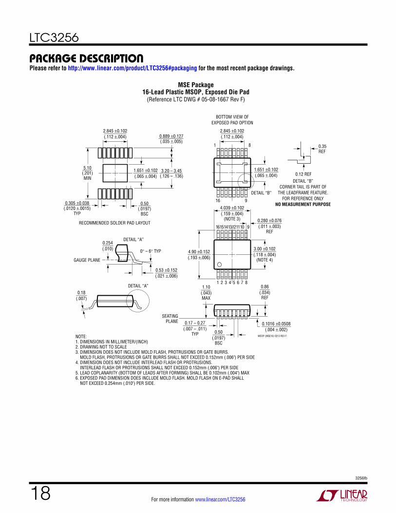
package DescripTionPlease refer to http://www.linear.com/product/LTC3256#packaging for the most recent package drawings.
MSOP (MSE16) 0213 REV F
0.53 ±0.152(.021 ±.006)
SEATINGPLANE
0.18(.007)
1.10(.043)MAX
0.17 – 0.27(.007 – .011)
TYP
0.86(.034)REF
0.50(.0197)
BSC
16
16151413121110
1 2 3 4 5 6 7 8
9
9
1 8
NOTE:1. DIMENSIONS IN MILLIMETER/(INCH)2. DRAWING NOT TO SCALE3. DIMENSION DOES NOT INCLUDE MOLD FLASH, PROTRUSIONS OR GATE BURRS. MOLD FLASH, PROTRUSIONS OR GATE BURRS SHALL NOT EXCEED 0.152mm (.006") PER SIDE4. DIMENSION DOES NOT INCLUDE INTERLEAD FLASH OR PROTRUSIONS. INTERLEAD FLASH OR PROTRUSIONS SHALL NOT EXCEED 0.152mm (.006") PER SIDE5. LEAD COPLANARITY (BOTTOM OF LEADS AFTER FORMING) SHALL BE 0.102mm (.004") MAX6. EXPOSED PAD DIMENSION DOES INCLUDE MOLD FLASH. MOLD FLASH ON E-PAD SHALL NOT EXCEED 0.254mm (.010") PER SIDE.
0.254(.010) 0° – 6° TYP
DETAIL “A”
DETAIL “A”
GAUGE PLANE
5.10(.201)MIN
3.20 – 3.45(.126 – .136)
0.889 ±0.127(.035 ±.005)
RECOMMENDED SOLDER PAD LAYOUT
0.305 ±0.038(.0120 ±.0015)
TYP
0.50(.0197)
BSC
BOTTOM VIEW OFEXPOSED PAD OPTION
2.845 ±0.102(.112 ±.004)
2.845 ±0.102(.112 ±.004)
4.039 ±0.102(.159 ±.004)
(NOTE 3)
1.651 ±0.102(.065 ±.004)
1.651 ±0.102(.065 ±.004)
0.1016 ±0.0508(.004 ±.002)
3.00 ±0.102(.118 ±.004)
(NOTE 4)
0.280 ±0.076(.011 ±.003)
REF
4.90 ±0.152(.193 ±.006)
DETAIL “B”
DETAIL “B”CORNER TAIL IS PART OF
THE LEADFRAME FEATURE.FOR REFERENCE ONLY
NO MEASUREMENT PURPOSE
0.12 REF
0.35REF
MSE Package16-Lead Plastic MSOP, Exposed Die Pad
(Reference LTC DWG # 05-08-1667 Rev F)

LTC3256
193256fb
For more information www.linear.com/LTC3256
Information furnished by Linear Technology Corporation is believed to be accurate and reliable. However, no responsibility is assumed for its use. Linear Technology Corporation makes no representa-tion that the interconnection of its circuits as described herein will not infringe on existing patent rights.
revision hisToryREV DATE DESCRIPTION PAGE NUMBER
A 08/16 Updated feature list 1
B 12/16 Changed Reset Timer Control (RT) conditionsChanged Watchdog Timer Control (WDT) conditionsChanged title of graph G12Modified 5V Output from 2:1 Charge Pump section
346
14
LTC3256
203256fb
For more information www.linear.com/LTC3256 LINEAR TECHNOLOGY CORPORATION 2016
LT 1216 REV B • PRINTED IN USALinear Technology Corporation1630 McCarthy Blvd., Milpitas, CA 95035-7417(408) 432-1900 ● FAX: (408) 434-0507 ● www.linear.com/LTC3256
relaTeD parTs
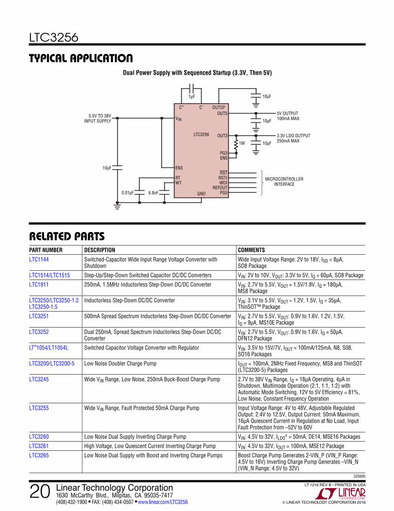
Typical applicaTion
1µF
10µF
0.01µF 6.8nF
10µF
10µF
10µF1M
MICROCONTROLLERINTERFACE
5V OUTPUT100mA MAX
3.3V LDO OUTPUT250mA MAX
5.5V TO 38VINPUT SUPPLY
C+ C– OUTCPOUT5
OUT3
EN5PG3
RSTI
REFOUT
RST
WDI
VIN
EN3
RTWT
GND
LTC3256
PG5
PART NUMBER DESCRIPTION COMMENTS
LTC1144 Switched-Capacitor Wide Input Range Voltage Converter with Shutdown
Wide Input Voltage Range: 2V to 18V, ISD < 8µA, SO8 Package
LTC1514/LTC1515 Step-Up/Step-Down Switched Capacitor DC/DC Converters VIN: 2V to 10V, VOUT: 3.3V to 5V, IQ = 60µA, SO8 Package
LTC1911 250mA, 1.5MHz Inductorless Step-Down DC/DC Converter VIN: 2.7V to 5.5V, VOUT = 1.5V/1.8V, IQ = 180µA, MS8 Package
LTC3250/LTC3250-1.2 LTC3250-1.5
Inductorless Step-Down DC/DC Converter VIN: 3.1V to 5.5V, VOUT = 1.2V, 1.5V, IQ = 35µA, ThinSOT™ Package
LTC3251 500mA Spread Spectrum Inductorless Step-Down DC/DC Converter VIN: 2.7V to 5.5V, VOUT: 0.9V to 1.6V, 1.2V, 1.5V, IQ = 9µA, MS10E Package
LTC3252 Dual 250mA, Spread Spectrum Inductorless Step-Down DC/DC Converter
VIN: 2.7V to 5.5V, VOUT: 0.9V to 1.6V, IQ = 50µA, DFN12 Package
LT®1054/LT1054L Switched Capacitor Voltage Converter with Regulator VIN: 3.5V to 15V/7V, IOUT = 100mA/125mA, N8, S08, SO16 Packages
LTC3200/LTC3200-5 Low Noise Doubler Charge Pump IOUT = 100mA, 2MHz Fixed Frequency, MS8 and ThinSOT (LTC3200-5) Packages
LTC3245 Wide VIN Range, Low Noise, 250mA Buck-Boost Charge Pump 2.7V to 38V VIN Range, IQ = 18µA Operating, 4µA in Shutdown, Multimode Operation (2:1, 1:1, 1:2) with Automatic Mode Switching, 12V to 5V Efficiency = 81%, Low Noise, Constant Frequency Operation
LTC3255 Wide VIN Range, Fault Protected 50mA Charge Pump Input Voltage Range: 4V to 48V, Adjustable Regulated Output: 2.4V to 12.5V, Output Current: 50mA Maximum, 16µA Quiescent Current in Regulation at No Load, Input Fault Protection from –52V to 60V
LTC3260 Low Noise Dual Supply Inverting Charge Pump VIN: 4.5V to 32V, ILDO± = 50mA, DE14, MSE16 Packages
LTC3261 High Voltage, Low Quiescent Current Inverting Charge Pump VIN: 4.5V to 32V, IOUT = 100mA, MSE12 Package
LTC3265 Low Noise Dual Supply with Boost and Inverting Charge Pumps Boost Charge Pump Generates 2-VIN_P (VIN_P Range: 4.5V to 16V) Inverting Charge Pump Generates –VIN_N (VIN_N Range: 4.5V to 32V)
Dual Power Supply with Sequenced Startup (3.3V, Then 5V)