ltc2977 - analog.com · l2977 2 2977 for more information table of contents features ..... 1
TRANSCRIPT
LTC2977
12977fc
For more information www.linear.com/LTC2977
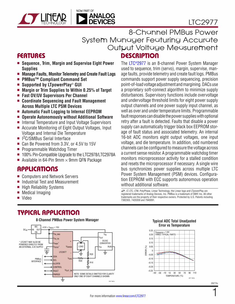
TYPICAL APPLICATION
FEATURES
APPLICATIONS
DESCRIPTION
8-Channel PMBus Power System Manager Featuring Accurate
Output Voltage Measurement
The LTC®2977 is an 8-channel Power System Manager used to sequence, trim (servo), margin, supervise, man-age faults, provide telemetry and create fault logs. PMBus commands support power supply sequencing, precision point-of-load voltage adjustment and margining. DACs use a proprietary soft-connect algorithm to minimize supply disturbances. Supervisory functions include overvoltage and undervoltage threshold limits for eight power supply output channels and one power supply input channel, as well as over and under temperature limits. Programmable fault responses can disable the power supplies with optional retry after a fault is detected. Faults that disable a power supply can automatically trigger black box EEPROM stor-age of fault status and associated telemetry. An internal 16-bit ADC monitors eight output voltages, one input voltage, and die temperature. In addition, odd numbered channels can be configured to measure the voltage across a current sense resistor. A programmable watchdog timer monitors microprocessor activity for a stalled condition and resets the microprocessor if necessary. A single wire bus synchronizes power supplies across multiple LTC Power System Management (PSM) devices. Configura-tion EEPROM with ECC supports autonomous operation without additional software.
n Computers and Network Servers n Industrial Test and Measurement n High Reliability Systems n Medical Imaging n Video
n Sequence, Trim, Margin and Supervise Eight Power Supplies
n Manage Faults, Monitor Telemetry and Create Fault Logs n PMBus™ Compliant Command Set n Supported by LTpowerPlay® GUI n Margin or Trim Supplies to Within 0.25% of Target n Fast OV/UV Supervisors Per Channel n Coordinate Sequencing and Fault Management
Across Multiple LTC PSM Devices n Automatic Fault Logging to Internal EEPROM n Operate Autonomously without Additional Software n Internal Temperature and Input Voltage Supervisors n Accurate Monitoring of Eight Output Voltages, Input
Voltage and Internal Die Temperature n I2C/SMBus Serial Interface n Can Be Powered from 3.3V, or 4.5V to 15V n Programmable Watchdog Timer n 100% Pin-Compatible Upgrade to the LTC2978/LTC2978A n Available in 64-Pin 9mm × 9mm QFN Package
L, LT, LTC, LTM, PolyPhase, Linear Technology, the Linear logo and LTpowerPlay are registered trademarks of Analog Devices, Inc. PMBus is a trademark of SMIF, Inc. All other trademarks are the property of their respective owners. Protected by U.S. Patents including 7382303, 7420359 and 7940091.
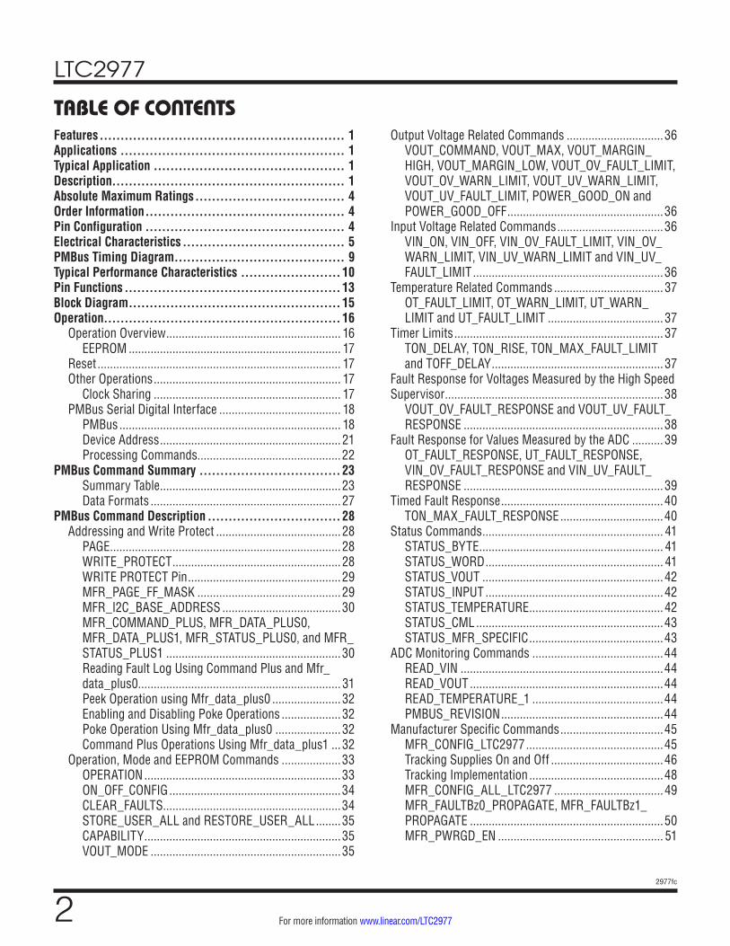
8-Channel PMBus Power System Manager Typical ADC Total Unadjusted Error vs Temperature
DCIN
R20
R10
2977 TA01a
R30
LOAD
VOUT
VFB
VIN
RUN
DC/DCCONVERTER
VSENSE
VDAC
VOUT_EN
VIN_SNS
VPWR*
VDD33*
IBC
ENIN OUT
4.5V ≤ VIBUS ≤ 15V
FAULT
PWRGD
SDA
SCL
ALERTB
CONTROL
PMBusINTERFACE
NOTE: SOME DETAILS OMITTED FOR CLARITYONLY ONE OF EIGHT CHANNELS SHOWN
* LTC2977 MAY ALSO BEPOWERED DIRECTLY FROMAN EXTERNAL 3.3V SUPPLY
+
–LTC2977
VIN_EN
TEMPERATURE (°C)–50
–0.25
ERRO
R (%
)
–0.05
–0.10
–0.15
–0.20
0.05
0.10
0.15
0.25
50
2977 TA01b
0
0.20
10 90 110–30 –10 30 70
VSENSEP0 = 1.8VTHREE TYPICAL PARTS
LTC2977
22977fc
For more information www.linear.com/LTC2977
TABLE OF CONTENTSFeatures ........................................................... 1Applications ...................................................... 1Typical Application .............................................. 1Description........................................................ 1Absolute Maximum Ratings .................................... 4Order Information ................................................ 4Pin Configuration ................................................ 4Electrical Characteristics ....................................... 5PMBus Timing Diagram ......................................... 9Typical Performance Characteristics ........................ 10Pin Functions .................................................... 13Block Diagram ................................................... 15Operation......................................................... 16
Operation Overview ........................................................ 16EEPROM .................................................................... 17
Reset .............................................................................. 17Other Operations ............................................................ 17
Clock Sharing ............................................................ 17PMBus Serial Digital Interface ....................................... 18
PMBus ....................................................................... 18Device Address .......................................................... 21Processing Commands..............................................22
PMBus Command Summary .................................. 23Summary Table ..........................................................23Data Formats ............................................................. 27
PMBus Command Description ................................ 28Addressing and Write Protect ........................................ 28
PAGE .......................................................................... 28WRITE_PROTECT ...................................................... 28WRITE PROTECT Pin .................................................29MFR_PAGE_FF_MASK ..............................................29MFR_I2C_BASE_ADDRESS ......................................30MFR_COMMAND_PLUS, MFR_DATA_PLUS0, MFR_DATA_PLUS1, MFR_STATUS_PLUS0, and MFR_STATUS_PLUS1 ........................................................30Reading Fault Log Using Command Plus and Mfr_data_plus0 ................................................................. 31Peek Operation using Mfr_data_plus0 ...................... 32Enabling and Disabling Poke Operations ...................32Poke Operation Using Mfr_data_plus0 ..................... 32Command Plus Operations Using Mfr_data_plus1 ...32
Operation, Mode and EEPROM Commands ...................33OPERATION ...............................................................33ON_OFF_CONFIG .......................................................34CLEAR_FAULTS .........................................................34STORE_USER_ALL and RESTORE_USER_ALL ........35CAPABILITY ...............................................................35VOUT_MODE .............................................................35
Output Voltage Related Commands ...............................36VOUT_COMMAND, VOUT_MAX, VOUT_MARGIN_HIGH, VOUT_MARGIN_LOW, VOUT_OV_FAULT_LIMIT, VOUT_OV_WARN_LIMIT, VOUT_UV_WARN_LIMIT, VOUT_UV_FAULT_LIMIT, POWER_GOOD_ON and POWER_GOOD_OFF ..................................................36
Input Voltage Related Commands ..................................36VIN_ON, VIN_OFF, VIN_OV_FAULT_LIMIT, VIN_OV_WARN_LIMIT, VIN_UV_WARN_LIMIT and VIN_UV_FAULT_LIMIT .............................................................36
Temperature Related Commands ................................... 37OT_FAULT_LIMIT, OT_WARN_LIMIT, UT_WARN_LIMIT and UT_FAULT_LIMIT ..................................... 37
Timer Limits ................................................................... 37TON_DELAY, TON_RISE, TON_MAX_FAULT_LIMIT and TOFF_DELAY ....................................................... 37
Fault Response for Voltages Measured by the High Speed Supervisor ......................................................................38
VOUT_OV_FAULT_RESPONSE and VOUT_UV_FAULT_RESPONSE ................................................................38
Fault Response for Values Measured by the ADC ..........39OT_FAULT_RESPONSE, UT_FAULT_RESPONSE, VIN_OV_FAULT_RESPONSE and VIN_UV_FAULT_RESPONSE ................................................................39
Timed Fault Response ....................................................40TON_MAX_FAULT_RESPONSE .................................40
Status Commands .......................................................... 41STATUS_BYTE ........................................................... 41STATUS_WORD ......................................................... 41STATUS_VOUT .......................................................... 42STATUS_INPUT ......................................................... 42STATUS_TEMPERATURE ........................................... 42STATUS_CML ............................................................43STATUS_MFR_SPECIFIC ...........................................43
ADC Monitoring Commands ..........................................44READ_VIN .................................................................44READ_VOUT ..............................................................44READ_TEMPERATURE_1 ..........................................44PMBUS_REVISION ....................................................44
Manufacturer Specific Commands .................................45MFR_CONFIG_LTC2977 ............................................45Tracking Supplies On and Off ....................................46Tracking Implementation ...........................................48MFR_CONFIG_ALL_LTC2977 ...................................49MFR_FAULTBz0_PROPAGATE, MFR_FAULTBz1_PROPAGATE ..............................................................50MFR_PWRGD_EN ..................................................... 51
LTC2977
32977fc
For more information www.linear.com/LTC2977
TABLE OF CONTENTSMFR_FAULTB00_RESPONSE, MFR_FAULTB01_RESPONSE, MFR_FAULTB10_RESPONSE and MFR_FAULTB11_RESPONSE .............................................. 52MFR_VINEN_OV_FAULT_RESPONSE ........................53MFR_VINEN_UV_FAULT_RESPONSE ........................54MFR_RETRY_COUNT ................................................55MFR_RETRY_DELAY .................................................55MFR_RESTART_DELAY .............................................55MFR_VOUT_PEAK .....................................................56MFR_VIN_PEAK ........................................................56MFR_TEMPERATURE_PEAK .....................................56MFR_DAC ..................................................................56MFR_POWERGOOD_ASSERTION_DELAY ................ 57MFR_PADS ................................................................ 57MFR_SPECIAL_ID .....................................................58MFR_SPECIAL_LOT ..................................................58MFR_INFO .................................................................58MFR_VOUT_DISCHARGE_THRESHOLD .................... 59MFR_COMMON ......................................................... 59USER_DATA_00, USER_DATA_01, USER_DATA_02, USER_DATA_03, USER_DATA_04, MFR_LTC_RESERVED_1 and MFR_LTC_RESERVED_2 .............60MFR_VOUT_MIN .......................................................60MFR_VIN_MIN ..........................................................60MFR_TEMPERATURE_MIN ....................................... 61MFR_STATUS_2 ........................................................ 61MFR_TELEMETRY .....................................................62
Watchdog Operation ......................................................63MFR_WATCHDOG_T_FIRST and MFR_WATCHDOG_T ..................................................63
Bulk Programming the User EEPROM Space .................63MFR_EE_UNLOCK .....................................................64MFR_EE_ERASE .......................................................64MFR_EE_DATA ..........................................................64Response When Part Is Busy ....................................65MFR_EE Erase and Write Programming Time ...........65
Fault Log Operation ........................................................65MFR_FAULT_LOG_STORE ........................................65MFR_FAULT_LOG_RESTORE ....................................65MFR_FAULT_LOG_CLEAR ........................................66MFR_FAULT_LOG_STATUS .......................................66MFR_FAULT_LOG ......................................................67
Applications Information ...................................... 74Overview ........................................................................ 74Powering the LTC2977 ................................................... 74Setting Command Register Values ................................. 74Sequence, Servo, Margin and Restart Operations ......... 74
Command Units On or Off ......................................... 74On Sequencing .......................................................... 75
On State Operation .................................................... 75Servo Modes ............................................................. 75DAC Modes ................................................................ 75Margining .................................................................. 76Off Sequencing .......................................................... 76VOUT Off Threshold Voltage ....................................... 76Automatic Restart Via MFR_RESTART_DELAY Command and CONTROLn pin .................................. 76
Fault Management .......................................................... 76Output Overvoltage and Undervoltage Faults ............ 76Output Overvoltage and Undervoltage Warnings ......77Configuring the VIN_EN Output ..................................77Multichannel Fault Management ............................... 79
Interconnect Between Multiple LTC2977’s ..................... 79Application Circuits ........................................................80
Trimming and Margining DC/DC Converters with External Feedback Resistors .....................................80Four-Step Resistor Selection Procedure for DC/DC Converters with External Feedback Resistors ........... 81Trimming and Margining DC/DC Converters with a TRIM Pin ....................................................................82Two-Step Resistor and DAC Full-Scale Voltage Selection Procedure for DC/DC Converters with a TRIM Pin ....................................................................82Measuring Current .....................................................82Measuring Current with a Sense Resistor .................83Measuring Current with Inductor DCR ......................83Single Phase Design Example ...................................83Measuring Multiphase Currents ................................83Multiphase Design Example ......................................84Anti-aliasing Filter Considerations .............................84Sensing Negative Voltages ........................................85
Connecting the DC1613 USB to I2C/SMBus/PMBus Controller to the LTC2977 in System .............................85Design Checklist ............................................................. 87
Logic Signals ............................................................. 87DAC Outputs .............................................................. 87
LTpowerPlay: An Interactive GUI for Power System Managers ....................................................................... 87PCB Assembly and Layout Suggestions ........................88
Bypass Capacitor Placement .....................................88Exposed Pad Stencil Design ......................................88PC Board Layout ........................................................89Unused ADC Sense Inputs .........................................89
Package Description ........................................... 90Revision History ................................................ 91Typical Application ............................................. 92Related Parts .................................................... 92
LTC2977
42977fc
For more information www.linear.com/LTC2977
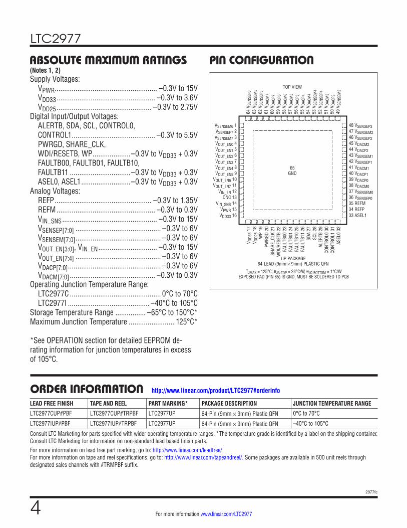
PIN CONFIGURATIONABSOLUTE MAXIMUM RATINGSSupply Voltages: VPWR...................................................... –0.3V to 15V VDD33 .................................................... –0.3V to 3.6V VDD25 .................................................. –0.3V to 2.75VDigital Input/Output Voltages: ALERTB, SDA, SCL, CONTROL0, CONTROL1 ............................................ –0.3V to 5.5V PWRGD, SHARE_CLK, WDI/RESETB, WP ....................–0.3V to VDD33 + 0.3V FAULTB00, FAULTB01, FAULTB10, FAULTB11 ................................–0.3V to VDD33 + 0.3V ASEL0, ASEL1 ..........................–0.3V to VDD33 + 0.3VAnalog Voltages: REFP ................................................... –0.3V to 1.35V REFM .................................................... –0.3V to 0.3V
VIN_SNS .................................................. –0.3V to 15V VSENSEP[7:0] ............................................. –0.3V to 6V
VSENSEM[7:0] ............................................. –0.3V to 6V VOUT_EN[3:0], VIN_EN ............................... –0.3V to 15V VOUT_EN[7:4] ............................................. –0.3V to 6V VDACP[7:0] ................................................. –0.3V to 6V VDACM[7:0] ............................................. –0.3V to 0.3VOperating Junction Temperature Range: LTC2977C ................................................ 0°C to 70°C LTC2977I ........................................... –40°C to 105°CStorage Temperature Range ................ –65°C to 150°C*Maximum Junction Temperature ........................ 125°C*
*See OPERATION section for detailed EEPROM de-rating information for junction temperatures in excess of 105°C.
(Notes 1, 2)
TOP VIEW
65GND
UP PACKAGE64-LEAD (9mm × 9mm) PLASTIC QFN
VSENSEM6 1VSENSEP7 2VSENSEM7 3VOUT_EN0 4VOUT_EN1 5VOUT_EN2 6VOUT_EN3 7VOUT_EN4 8VOUT_EN5 9
VOUT_EN6 10VOUT_EN7 11
VIN_EN 12DNC 13
VIN_SNS 14VPWR 15VDD33 16
48 VSENSEP347 VSENSEM246 VSENSEP245 VDACM244 VDACP243 VSENSEM142 VSENSEP141 VDACM140 VDACP139 VDACP038 VDACM037 VSENSEM036 VSENSEP035 REFM34 REFP33 ASEL1
64 V
SENS
EP6
63 V
SENS
EM5
62 V
SENS
EP5
61 V
DACM
760
VDA
CP7
59 V
DACP
658
VDA
CM6
57 V
DACM
556
VDA
CP5
55 V
DACP
454
VDA
CM4
53 V
SENS
EM4
52 V
SENS
EP4
51 V
DACM
350
VDA
CP3
49 V
SENS
EM3
V DD3
3 17
V DD2
5 18
WP
19PW
RGD
20SH
ARE_
CLK
21W
DI/R
ESET
B 22
FAUL
TB00
23
FAUL
TB01
24
FAUL
TB10
25
FAUL
TB11
26
SDA
27SC
L 28
ALER
TB 2
9CO
NTRO
L0 3
0CO
NTRO
L1 3
1AS
EL0
32
TJMAX = 125°C, θJA-TOP = 28°C/W, θJC-BOTTOM = 1°C/W
EXPOSED PAD (PIN 65) IS GND, MUST BE SOLDERED TO PCB
ORDER INFORMATIONLEAD FREE FINISH TAPE AND REEL PART MARKING* PACKAGE DESCRIPTION JUNCTION TEMPERATURE RANGE
LTC2977CUP#PBF LTC2977CUP#TRPBF LTC2977UP 64-Pin (9mm × 9mm) Plastic QFN 0°C to 70°C
LTC2977IUP#PBF LTC2977IUP#TRPBF LTC2977UP 64-Pin (9mm × 9mm) Plastic QFN –40°C to 105°C
Consult LTC Marketing for parts specified with wider operating temperature ranges. *The temperature grade is identified by a label on the shipping container. Consult LTC Marketing for information on non-standard lead based finish parts.For more information on lead free part marking, go to: http://www.linear.com/leadfree/ For more information on tape and reel specifications, go to: http://www.linear.com/tapeandreel/. Some packages are available in 500 unit reels through designated sales channels with #TRMPBF suffix.
http://www.linear.com/product/LTC2977#orderinfo
LTC2977
52977fc
For more information www.linear.com/LTC2977
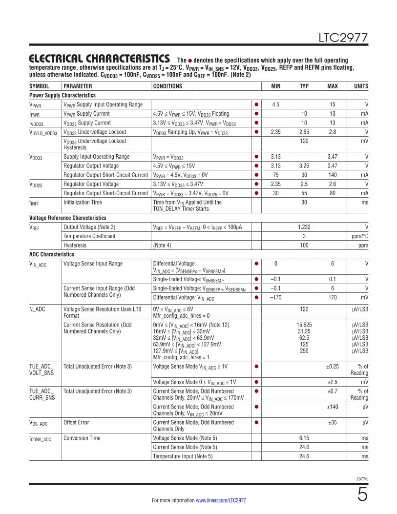
ELECTRICAL CHARACTERISTICS The l denotes the specifications which apply over the full operating temperature range, otherwise specifications are at TJ = 25°C. VPWR = VIN_SNS = 12V, VDD33, VDD25, REFP and REFM pins floating, unless otherwise indicated. CVDD33 = 100nF, CVDD25 = 100nF and CREF = 100nF. (Note 2)
SYMBOL PARAMETER CONDITIONS MIN TYP MAX UNITS
Power Supply Characteristics
VPWR VPWR Supply Input Operating Range l 4.5 15 V
IPWR VPWR Supply Current 4.5V ≤ VPWR ≤ 15V, VDD33 Floating l 10 13 mA
IVDD33 VDD33 Supply Current 3.13V ≤ VDD33 ≤ 3.47V, VPWR = VDD33 l 10 13 mA
VUVLO_VDD33 VDD33 Undervoltage Lockout VDD33 Ramping Up, VPWR = VDD33 l 2.35 2.55 2.8 V
VDD33 Undervoltage Lockout Hysteresis
120 mV
VDD33 Supply Input Operating Range VPWR = VDD33 l 3.13 3.47 V
Regulator Output Voltage 4.5V ≤ VPWR ≤ 15V l 3.13 3.26 3.47 V
Regulator Output Short-Circuit Current VPWR = 4.5V, VDD33 = 0V l 75 90 140 mA
VDD25 Regulator Output Voltage 3.13V ≤ VDD33 ≤ 3.47V l 2.35 2.5 2.6 V
Regulator Output Short-Circuit Current VPWR = VDD33 = 3.47V, VDD25 = 0V l 30 55 80 mA
tINIT Initialization Time Time from VIN Applied Until the TON_DELAY Timer Starts
30 ms
Voltage Reference Characteristics
VREF Output Voltage (Note 3) VREF = VREFP – VREFM, 0 < IREFP < 100µA 1.232 V
Temperature Coefficient 3 ppm/°C
Hysteresis (Note 4) 100 ppm
ADC Characteristics
VIN_ADC Voltage Sense Input Range Differential Voltage: VIN_ADC = (VSENSEPn – VSENSEMn)
l 0 6 V
Single-Ended Voltage: VSENSEMn l –0.1 0.1 V
Current Sense Input Range (Odd Numbered Channels Only)
Single-Ended Voltage: VSENSEPn, VSENSEMn l –0.1 6 V
Differential Voltage: VIN_ADC l –170 170 mV
N_ADC Voltage Sense Resolution Uses L16 Format
0V ≤ VIN_ADC ≤ 6V Mfr_config_adc_hires = 0
122 µV/LSB
Current Sense Resolution (Odd Numbered Channels Only)
0mV ≤ |VIN_ADC| < 16mV (Note 12) 16mV ≤ |VIN_ADC| < 32mV 32mV ≤ |VIN_ADC| < 63.9mV 63.9mV ≤ |VIN_ADC| < 127.9mV 127.9mV ≤ |VIN_ADC| Mfr_config_adc_hires = 1
15.625 31.25 62.5 125 250
µV/LSB µV/LSB µV/LSB µV/LSB µV/LSB
TUE_ADC_VOLT_SNS
Total Unadjusted Error (Note 3) Voltage Sense Mode VIN_ADC ≥ 1V l ±0.25 % of Reading
Voltage Sense Mode 0 ≤ VIN_ADC ≤ 1V l ±2.5 mV
TUE_ADC_CURR_SNS
Total Unadjusted Error (Note 3) Current Sense Mode, Odd Numbered Channels Only, 20mV ≤ VIN_ADC ≤ 170mV
l ±0.7 % of Reading
Current Sense Mode, Odd Numbered Channels Only, VIN_ADC ≤ 20mV
l ±140 µV
VOS_ADC Offset Error Current Sense Mode, Odd Numbered Channels Only
l ±35 µV
tCONV_ADC Conversion Time Voltage Sense Mode (Note 5) 6.15 ms
Current Sense Mode (Note 5) 24.6 ms
Temperature Input (Note 5) 24.6 ms
LTC2977
62977fc
For more information www.linear.com/LTC2977
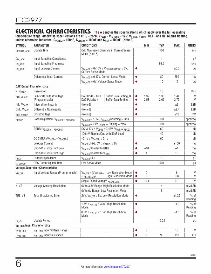
ELECTRICAL CHARACTERISTICS The l denotes the specifications which apply over the full operating temperature range, otherwise specifications are at TJ = 25°C. VPWR = VIN_SNS = 12V; VDD33, VDD25, REFP and REFM pins floating, unless otherwise indicated. CVDD33 = 100nF, CVDD25 = 100nF and CREF = 100nF. (Note 2)
SYMBOL PARAMETER CONDITIONS MIN TYP MAX UNITS
tUPDATE_ADC Update Time Odd Numbered Channels in Current Sense Mode (Note 5)
160 ms
CIN_ADC Input Sampling Capacitance 1 pF
fIN_ADC Input Sampling Frequency 62.5 kHz
IIN_ADC Input Leakage Current VIN_ADC = 0V, 0V ≤ VCOMMONMODE ≤ 6V, Current Sense Mode
l ±0.5 µA
Differential Input Current VIN_ADC = 0.17V, Current Sense Mode l 80 250 nA
VIN_ADC = 6V, Voltage Sense Mode l 10 15 µA
DAC Output Characteristics
N_VDACP Resolution 10 Bits
VFS_VDACP Full-Scale Output Voltage (Programmable)
DAC Code = 0x3FF DAC Polarity = 1
Buffer Gain Setting_0 Buffer Gain Setting_1
l
l
1.32 2.53
1.38 2.65
1.44 2.77
V V
INL_VDACP Integral Nonlinearity (Note 6) l ±2 LSB
DNL_VDACP Differential Nonlinearity (Note 6) l ±2.4 LSB
VOS_VDACP Offset Voltage (Note 6) l ±10 mV
VDACP Load Regulation (VDACPn – VDACMn) VDACPn = 2.65V, IVDACPn Sourcing = 2mA 100 ppm/mA
VDACPn = 0.1V, IVDACPn Sinking = 2mA 100 ppm/mA
PSRR (VDACPn – VDACMn) DC: 3.13V ≤ VDD33 ≤ 3.47V, VPWR = VDD33 60 dB
100mV Step in 20ns with 50pF Load 40 dB
DC CMRR (VDACPn – VDACMn) –0.1V ≤ VDACMn ≤ 0.1V 60 dB
Leakage Current VDACPn Hi-Z, 0V ≤ VDACPn ≤ 6V l ±100 nA
Short-Circuit Current Low VDACPn Shorted to GND l –10 –4 mA
Short-Circuit Current High VDACPn Shorted to VDD33 l 4 10 mA
COUT Output Capacitance VDACPn Hi-Z 10 pF
tS_VDACP DAC Output Update Rate Fast Servo Mode 500 µs
Voltage Supervisor Characteristics
VIN_VS Input Voltage Range (Programmable) VIN_VS = (VSENSEPn – VSENSEMn)
Low Resolution Mode High Resolution Mode
l
l
0 0
6 3.8
V V
Single-Ended Voltage: VSENSEMn l –0.1 0.1 V
N_VS Voltage Sensing Resolution 0V to 3.8V Range: High Resolution Mode 4 mV/LSB
0V to 6V Range: Low Resolution Mode 8 mV/LSB
TUE_VS Total Unadjusted Error 2V ≤ VIN_VS ≤ 6V, Low Resolution Mode l ±1.25 % of Reading
1.5V < VIN_VS ≤ 3.8V, High Resolution Mode
l ±1.0 % of Reading
0.8V ≤ VIN_VS ≤ 1.5V, High Resolution Mode
l ±1.5 % of Reading
tS_VS Update Period 12.21 µs
VIN_SNS Input Characteristics
VVIN_SNS VIN_SNS Input Voltage Range l 0 15 V
RVIN_SNS VIN_SNS Input Resistance l 70 90 110 kΩ
LTC2977
72977fc
For more information www.linear.com/LTC2977
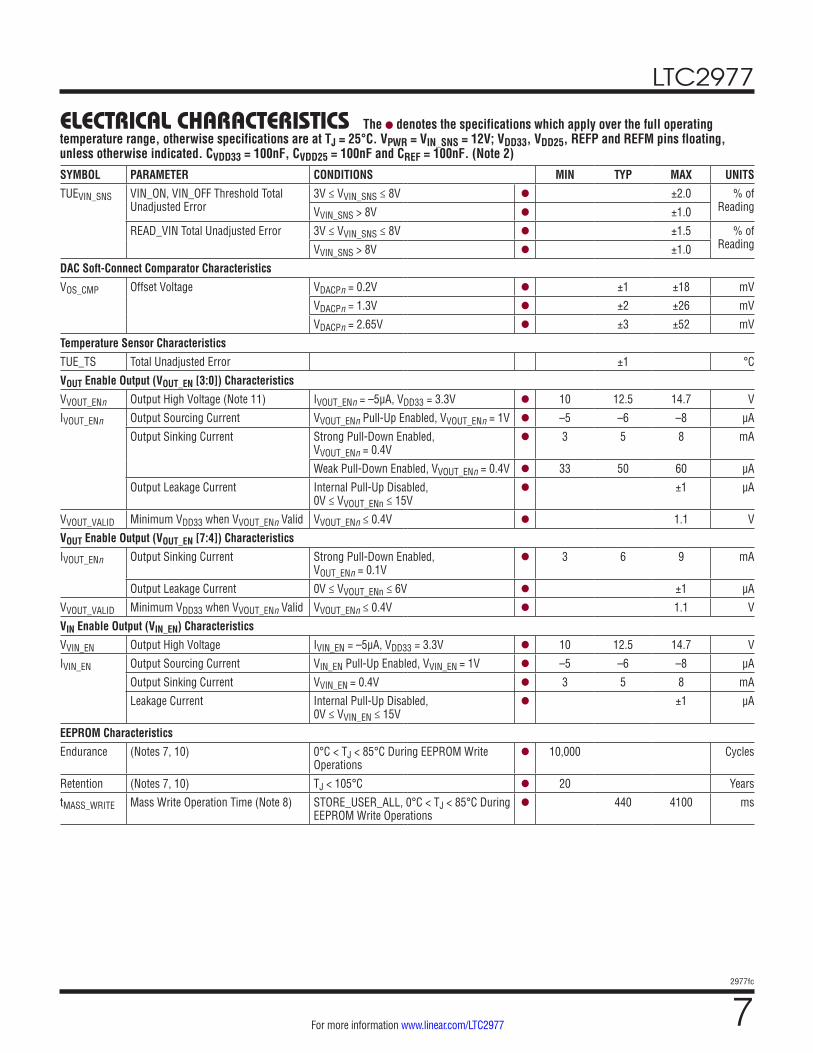
ELECTRICAL CHARACTERISTICS The l denotes the specifications which apply over the full operating temperature range, otherwise specifications are at TJ = 25°C. VPWR = VIN_SNS = 12V; VDD33, VDD25, REFP and REFM pins floating, unless otherwise indicated. CVDD33 = 100nF, CVDD25 = 100nF and CREF = 100nF. (Note 2)
SYMBOL PARAMETER CONDITIONS MIN TYP MAX UNITS
TUEVIN_SNS VIN_ON, VIN_OFF Threshold Total Unadjusted Error
3V ≤ VVIN_SNS ≤ 8V l ±2.0 % of ReadingVVIN_SNS > 8V l ±1.0
READ_VIN Total Unadjusted Error 3V ≤ VVIN_SNS ≤ 8V l ±1.5 % of ReadingVVIN_SNS > 8V l ±1.0
DAC Soft-Connect Comparator Characteristics
VOS_CMP Offset Voltage VDACPn = 0.2V l ±1 ±18 mV
VDACPn = 1.3V l ±2 ±26 mV
VDACPn = 2.65V l ±3 ±52 mV
Temperature Sensor Characteristics
TUE_TS Total Unadjusted Error ±1 °C
VOUT Enable Output (VOUT_EN [3:0]) Characteristics
VVOUT_ENn Output High Voltage (Note 11) IVOUT_ENn = –5µA, VDD33 = 3.3V l 10 12.5 14.7 V
IVOUT_ENn Output Sourcing Current VVOUT_ENn Pull-Up Enabled, VVOUT_ENn = 1V l –5 –6 –8 µA
Output Sinking Current Strong Pull-Down Enabled, VVOUT_ENn = 0.4V
l 3 5 8 mA
Weak Pull-Down Enabled, VVOUT_ENn = 0.4V l 33 50 60 µA
Output Leakage Current Internal Pull-Up Disabled, 0V ≤ VVOUT_ENn ≤ 15V
l ±1 µA
VVOUT_VALID Minimum VDD33 when VVOUT_ENn Valid VVOUT_ENn ≤ 0.4V l 1.1 V
VOUT Enable Output (VOUT_EN [7:4]) Characteristics
IVOUT_ENn Output Sinking Current Strong Pull-Down Enabled, VOUT_ENn = 0.1V
l 3 6 9 mA
Output Leakage Current 0V ≤ VVOUT_ENn ≤ 6V l ±1 µA
VVOUT_VALID Minimum VDD33 when VVOUT_ENn Valid VVOUT_ENn ≤ 0.4V l 1.1 V
VIN Enable Output (VIN_EN) Characteristics
VVIN_EN Output High Voltage IVIN_EN = –5µA, VDD33 = 3.3V l 10 12.5 14.7 V
IVIN_EN Output Sourcing Current VIN_EN Pull-Up Enabled, VVIN_EN = 1V l –5 –6 –8 µA
Output Sinking Current VVIN_EN = 0.4V l 3 5 8 mA
Leakage Current Internal Pull-Up Disabled, 0V ≤ VVIN_EN ≤ 15V
l ±1 µA
EEPROM Characteristics
Endurance (Notes 7, 10) 0°C < TJ < 85°C During EEPROM Write Operations
l 10,000 Cycles
Retention (Notes 7, 10) TJ < 105°C l 20 Years
tMASS_WRITE Mass Write Operation Time (Note 8) STORE_USER_ALL, 0°C < TJ < 85°C During EEPROM Write Operations
l 440 4100 ms
LTC2977
82977fc
For more information www.linear.com/LTC2977
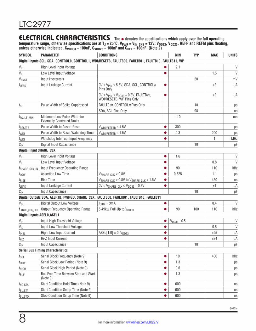
ELECTRICAL CHARACTERISTICS The l denotes the specifications which apply over the full operating temperature range, otherwise specifications are at TJ = 25°C. VPWR = VIN_SNS = 12V; VDD33, VDD25, REFP and REFM pins floating, unless otherwise indicated. CVDD33 = 100nF, CVDD25 = 100nF and CREF = 100nF. (Note 2)
SYMBOL PARAMETER CONDITIONS MIN TYP MAX UNITS
Digital Inputs SCL, SDA, CONTROL0, CONTROL1, WDI/RESETB, FAULTB00, FAULTB01, FAULTB10, FAULTB11, WP
VIH High Level Input Voltage l 2.1 V
VIL Low Level Input Voltage l 1.5 V
VHYST Input Hysteresis 20 mV
ILEAK Input Leakage Current 0V ≤ VPIN ≤ 5.5V, SDA, SCL, CONTROLn Pins Only
l ±2 µA
0V ≤ VPIN ≤ VDD33 + 0.3V, FAULTBzn, WDI/RESETB, WP Pins Only
l ±2 µA
tSP Pulse Width of Spike Suppressed FAULTBzn, CONTROLn Pins Only 10 µs
SDA, SCL Pins Only 98 ns
tFAULT_MIN Minimum Low Pulse Width for Externally Generated Faults
110 ms
tRESETB Pulse Width to Assert Reset VWDI/RESETB ≤ 1.5V l 300 µs
tWDI Pulse Width to Reset Watchdog Timer VWDI/RESETB ≤ 1.5V l 0.3 200 µs
fWDI Watchdog Interrupt Input Frequency l 1 MHz
CIN Digital Input Capacitance 10 pF
Digital Input SHARE_CLK
VIH High Level Input Voltage l 1.6 V
VIL Low Level Input Voltage l 0.8 V
fSHARE_CLK_IN Input Frequency Operating Range l 90 110 kHz
tLOW Assertion Low Time VSHARE_CLK < 0.8V l 0.825 1.1 µs
tRISE Rise Time VSHARE_CLK < 0.8V to VSHARE_CLK > 1.6V l 450 ns
ILEAK Input Leakage Current 0V ≤ VSHARE_CLK ≤ VDD33 + 0.3V l ±1 µA
CIN Input Capacitance 10 pF
Digital Outputs SDA, ALERTB, PWRGD, SHARE_CLK, FAULTB00, FAULTB01, FAULTB10, FAULTB11
VOL Digital Output Low Voltage ISINK = 3mA l 0.4 V
fSHARE_CLK_OUT Output Frequency Operating Range 5.49kΩ Pull-Up to VDD33 l 90 100 110 kHz
Digital Inputs ASEL0,ASEL1
VIH Input High Threshold Voltage l VDD33 – 0.5 V
VIL Input Low Threshold Voltage l 0.5 V
IIH,IL High, Low Input Current ASEL[1:0] = 0, VDD33 l ±95 µA
IHIZ Hi-Z Input Current l ±24 µA
CIN Input Capacitance 10 pF
Serial Bus Timing Characteristics
fSCL Serial Clock Frequency (Note 9) l 10 400 kHz
tLOW Serial Clock Low Period (Note 9) l 1.3 µs
tHIGH Serial Clock High Period (Note 9) l 0.6 µs
tBUF Bus Free Time Between Stop and Start (Note 9)
l 1.3 µs
tHD,STA Start Condition Hold Time (Note 9) l 600 ns
tSU,STA Start Condition Setup Time (Note 9) l 600 ns
tSU,STO Stop Condition Setup Time (Note 9) l 600 ns
LTC2977
92977fc
For more information www.linear.com/LTC2977
The l denotes the specifications which apply over the full operating temperature range, otherwise specifications are at TJ = 25°C. VPWR = VIN_SNS = 12V; VDD33, VDD25, REFP and REFM pins floating, unless otherwise indicated. CVDD33 = 100nF, CVDD25 = 100nF and CREF = 100nF. (Note 2)
SYMBOL PARAMETER CONDITIONS MIN TYP MAX UNITS
tHD,DAT Data Hold Time (LTC2977 Receiving Data) (Note 9)
l 0 ns
Data Hold Time (LTC2977 Transmitting Data) (Note 9)
l 300 900 ns
tSU,DAT Data Setup Time (Note 9) l 100 ns
tSP Pulse Width of Spike Suppressed (Note 9)
98 ns
tTIMEOUT_BUS Time Allowed to Complete any PMBus Command After Which Time SDA Will Be Released and Command Terminated
Mfr_config_all_longer_pmbus_timeout = 0 Mfr_config_all_longer_pmbus_timeout = 1
l
l
25 200
35 280
ms ms
Additional Digital Timing Characteristics
tOFF_MIN Minimum Off Time for Any Channel 100 ms
Note 1: Stresses beyond those listed under Absolute Maximum Ratings may cause permanent damage to the device. Exposure to any Absolute Maximum Rating for extended periods may affect device reliability and lifetime.Note 2: All currents into device pins are positive. All currents out of device pins are negative. All voltages are referenced to GND unless otherwise specified. If power is supplied to the chip via the VDD33 pin only, connect VPWR and VDD33 pins together.Note 3: The ADC total unadjusted error includes all error sources. First, a two-point analog trim is performed to achieve a flat reference voltage (VREF) over temperature. This results in minimal temperature coefficient, but the absolute voltage can still vary. To compensate for this, a high-resolution, drift-free, and noiseless digital trim is applied at the output of the ADC, resulting in a very high accuracy measurement.Note 4: Hysteresis in the output voltage is created by package stress that differs depending on whether the IC was previously at a higher or lower temperature. Output voltage is always measured at 25°C, but the IC is cycled to 105°C or –40°C before successive measurements. Hysteresis is roughly proportional to the square of the temperature change. Note 5: The time between successive ADC conversions (latency of the ADC) for any given channel is given as: 36.9ms + (6.15ms • number of ADC channels configured in Low Resolution mode) + (24.6ms • number of ADC channels configured in High Resolution mode).
ELECTRICAL CHARACTERISTICS
Note 6: Nonlinearity is defined from the first code that is greater than or equal to the maximum offset specification to full-scale code, 1023.Note 7: EEPROM endurance and retention are guaranteed by design, characterization and correlation with statistical process controls. The minimum retention specification applies for devices whose EEPROM has been cycled less than the minimum endurance specification. Note 8: The LTC2977 will not acknowledge any PMBus commands except for MFR_COMMON, while a mass write operation is being executed. This includes the STORE_USER_ALL and MFR_FAULT_LOG_STORE commands or a fault log store initiated by a channel faulting off. Note 9: Maximum capacitive load, CB, for SCL and SDA is 400pF. Data and clock rise time (tr) and fall time (tf) are: (20 + 0.1 • CB) (ns) < tr < 300ns and (20 + 0.1 • CB) (ns) < tf < 300ns. CB = capacitance of one bus line in pF. SCL and SDA external pull-up voltage, VIO, is 3.13V < VIO < 5.5V. Note 10: EEPROM endurance and retention will be degraded when TJ > 105°C.Note 11: Output enable pins are charge-pumped from VDD33.Note 12: The current sense resolution is determined by the L11 format and the mV units of the returned value. For example, a full-scale value of 170mV returns an L11 value of 0xF2A8 = 680 • 2–2 = 170. This is the lowest range that can represent this value without overflowing the L11 mantissa and the resolution for 1LSB in this range is 2–2 mV = 250µV. Each successively lower range improves resolution by cutting the LSB size in half.
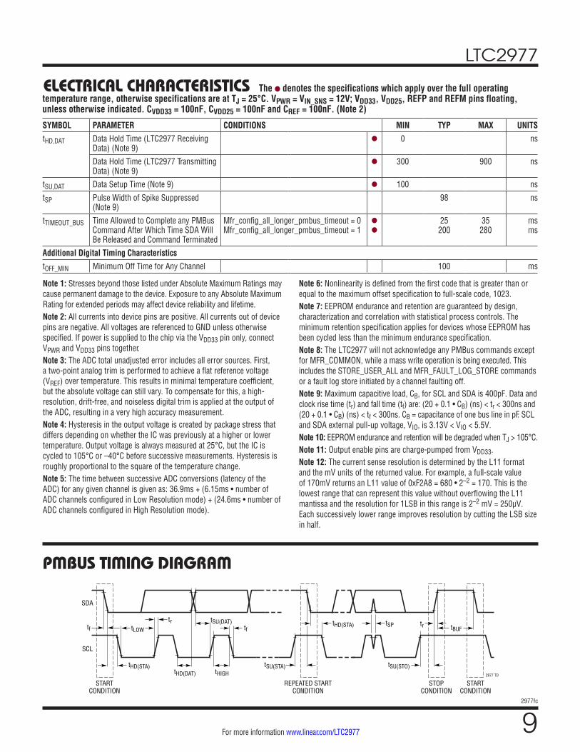
PMBUS TIMING DIAGRAM
SDA
SCL
tHD(STA)tHD(DAT)
tSU(STA) tSU(STO)
tSU(DAT)tLOW
tHD(STA) tSP tBUF
STARTCONDITION
STOPCONDITION
REPEATED STARTCONDITION
STARTCONDITION
trtf
trtf
tHIGH 2977 TD
LTC2977
102977fc
For more information www.linear.com/LTC2977
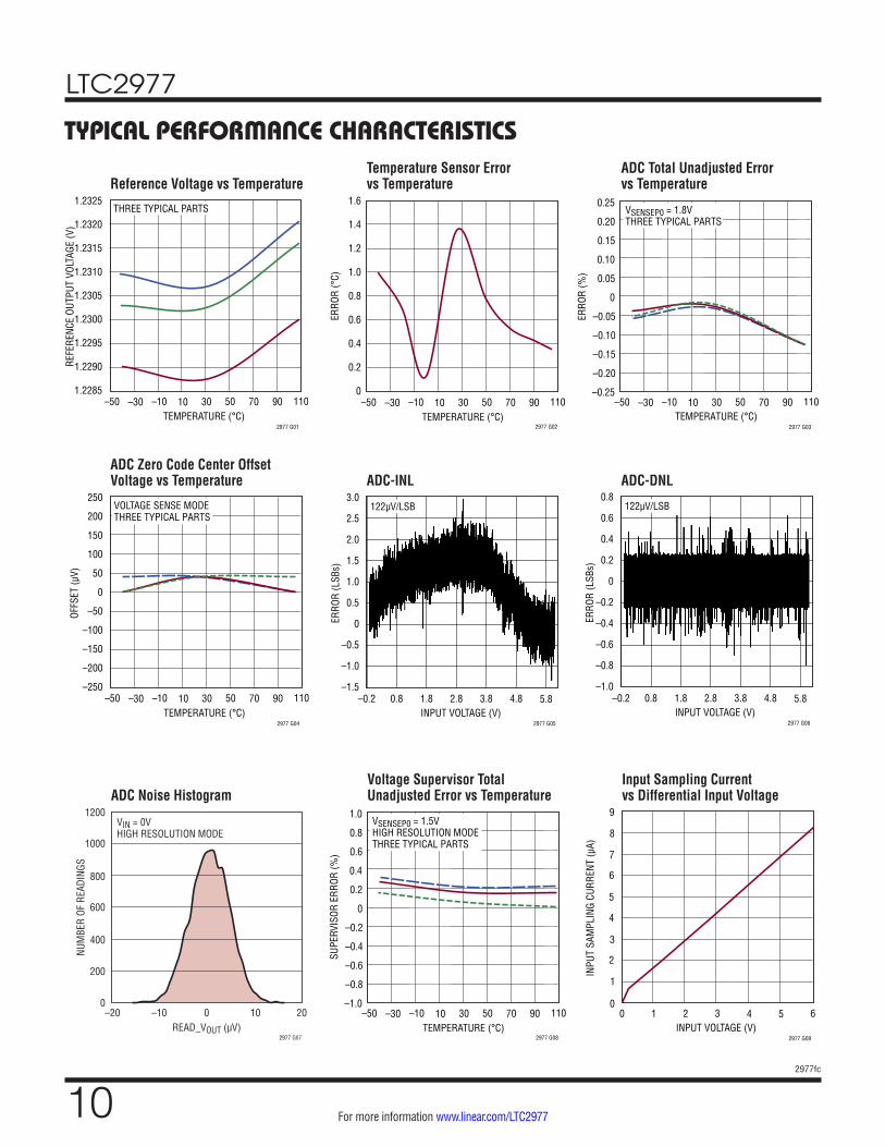
TYPICAL PERFORMANCE CHARACTERISTICS
Reference Voltage vs TemperatureTemperature Sensor Error vs Temperature
ADC Total Unadjusted Error vs Temperature
ADC Zero Code Center Offset Voltage vs Temperature ADC-INL ADC-DNL
TEMPERATURE (°C)
REFE
RENC
E OU
TPUT
VOL
TAGE
(V)
1.2325
1.2320
1.2315
1.2310
1.2305
1.2300
1.2295
1.2290
1.2285
2977 G01
THREE TYPICAL PARTS
–50 5010 90 110–30 –10 30 70TEMPERATURE (°C)
ERRO
R (°
C)
1.6
1.4
1.2
1.0
0.8
0.6
0.4
0.2
0
2977 G02
–50 5010 90 110–30 –10 30 70TEMPERATURE (°C)
–50–0.25
ERRO
R (%
)
–0.05
–0.10
–0.15
–0.20
0.05
0.10
0.15
0.25
50
2977 G03
0
0.20
10 90 110–30 –10 30 70
VSENSEP0 = 1.8VTHREE TYPICAL PARTS
TEMPERATURE (°C)
OFFS
ET (µ
V)
250
200
150
100
50
0
–50
–100
–150
–200
–250
2977 G04
VOLTAGE SENSE MODETHREE TYPICAL PARTS
–50 5010 90 110–30 –10 30 70INPUT VOLTAGE (V)
–0.2
ERRO
R (L
SBs)
5.8
3.0
2.5
2.0
1.5
1.0
0.5
0
–0.5
–1.0
–1.5
2977 G05
0.8 1.8 2.8 3.8 4.8
122µV/LSB
INPUT VOLTAGE (V)–0.2
ERRO
R (L
SBs)
5.8
0.8
0.6
0.4
0.2
0
–0.2
–0.4
–0.6
–0.8
–1.0
2977 G06
0.8 1.8 2.8 3.8 4.8
122µV/LSB
ADC Noise HistogramVoltage Supervisor Total Unadjusted Error vs Temperature
Input Sampling Current vs Differential Input Voltage
READ_VOUT (µV)–20
0
NUM
BER
OF R
EADI
NGS
200
400
600
800
1000
1200
–10 0 10 20
2977 G07
VIN = 0VHIGH RESOLUTION MODE
TEMPERATURE (°C)
SUPE
RVIS
OR E
RROR
(%)
2977 G08
–50–1.0
–0.2
–0.4
–0.6
–0.8
0.2
0
0.4
0.6
1.0
50
0.8
10 90 110–30 –10 30 70
VSENSEP0 = 1.5VHIGH RESOLUTION MODETHREE TYPICAL PARTS
INPUT VOLTAGE (V)0
0
INPU
T SA
MPL
ING
CURR
ENT
(µA)
1
3
4
5
4
9
2977 G09
2
21 53 6
6
7
8
LTC2977
112977fc
For more information www.linear.com/LTC2977
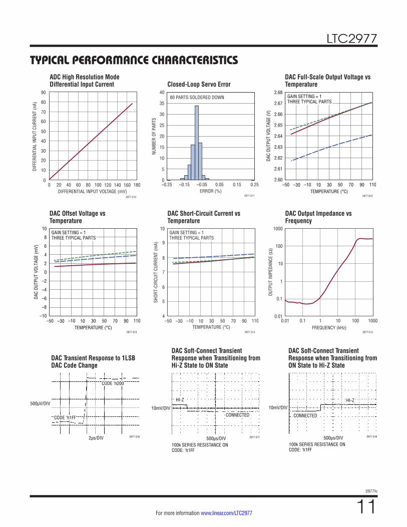
TYPICAL PERFORMANCE CHARACTERISTICSDAC Full-Scale Output Voltage vs Temperature
TEMPERATURE (°C)
DAC
OUTP
UT V
OLTA
GE (V
)
2.68
2.67
2.66
2.65
2.64
2.63
2.62
2.61
2.60
2977 G12
–50 5010 90 110–30 –10 30 70
GAIN SETTING = 1THREE TYPICAL PARTS
ADC High Resolution Mode Differential Input Current
DIFFERENTIAL INPUT VOLTAGE (mV)0
0
DIFF
EREN
TIAL
INPU
T CU
RREN
T (n
A)
10
30
40
50
120 140 160
90
2977 G10
20
6020 8040 100 180
60
70
80
DAC Offset Voltage vs Temperature
TEMPERATURE (°C)
DAC
OUTP
UT V
OLTA
GE (m
V)
10
8
6
4
2
0
–2
–4
–6
–8
–10
2977 G13
–50 5010 90 110–30 –10 30 70
GAIN SETTING = 1THREE TYPICAL PARTS
DAC Short-Circuit Current vs Temperature
TEMPERATURE (°C)
4
SHOR
T-CI
RCUI
T CU
RREN
T (m
A)
6
8
10
5
7
9
2977 G14
–50 5010 90 110–30 –10 30 70
GAIN SETTING = 1THREE TYPICAL PARTS
DAC Output Impedance vs Frequency
Closed-Loop Servo Error
FREQUENCY (kHz)0.01
OUTP
UT IM
PEDA
NCE
(Ω)10
100
1000
100
2977 G15
1
0.1
0.010.1 1 10 1000
DAC Transient Response to 1LSB DAC Code Change
DAC Soft-Connect Transient Response when Transitioning from Hi-Z State to ON State
DAC Soft-Connect Transient Response when Transitioning from ON State to Hi-Z State
10mV/DIV
500µs/DIV100k SERIES RESISTANCE ONCODE: ‘h1FF
2977 G17
HI-Z
CONNECTED
10mV/DIV
500µs/DIV100k SERIES RESISTANCE ONCODE: ‘h1FF
2977 G18
CONNECTED
HI-Z500µV/DIV
2µs/DIV 2977 G16
CODE ‘h1FF
CODE ‘h200
80 PARTS SOLDERED DOWN
ERROR (%)–0.25 –0.15 –0.05 0.05 0.15 0.250
5
10
15
20
25
30
35
40
NUM
BER
OF P
ARTS
2977 G11
LTC2977
122977fc
For more information www.linear.com/LTC2977
TYPICAL PERFORMANCE CHARACTERISTICS
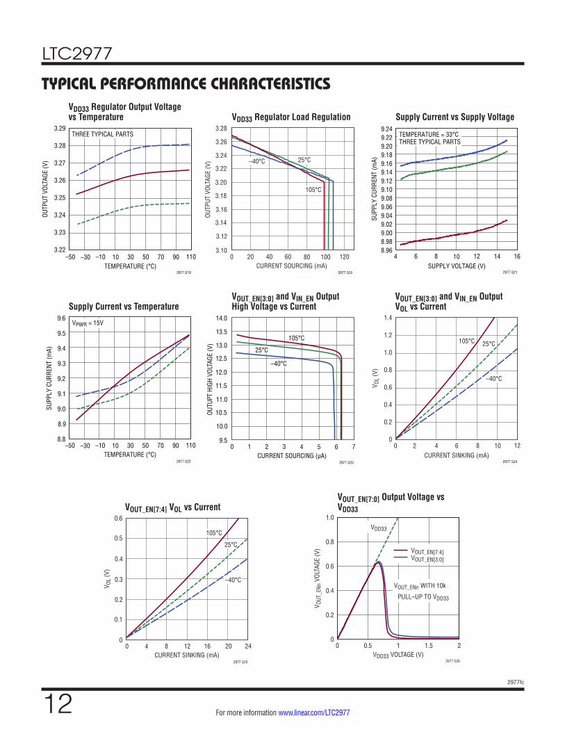
Supply Current vs Supply Voltage
Supply Current vs TemperatureVOUT_EN[3:0] and VIN_EN Output High Voltage vs Current
VDD33 Regulator Load Regulation
VOUT_EN[3:0] and VIN_EN Output VOL vs Current
VOUT_EN[7:4] VOL vs Current
CURRENT SOURCING (mA)0
3.10
OUTP
UT V
OLTA
GE (V
)
3.12
3.16
3.18
3.20
80
3.28
2977 G20
3.14
4020 10060 120
3.22
3.24
3.26
–40°C
105°C
25°C
SUPPLY VOLTAGE (V)4
SUPP
LY C
URRE
NT (m
A)
10 14
2977 G21
8.968.98
6 8 12
9.249.229.209.189.169.149.129.109.089.069.049.029.00
16
TEMPERATURE = 33°CTHREE TYPICAL PARTS
TEMPERATURE (°C)
8.8
SUPP
LY C
URRE
NT (m
A)
8.9
9.1
9.2
9.3
9.6
2977 G22
9.0
9.4
9.5
VPWR = 15V
–50 5010 90 110–30 –10 30 70CURRENT SINKING (mA)
0
1.4
1.2
1.0
0.8
0.6
0.4
0.2
06 10
2977 G24
2 4 8 12
V OL
(V)
105°C 25°C
–40°C
CURRENT SINKING (mA)0
0
V OL
(V)
0.1
0.2
0.3
0.4
0.6
4 8 12 16
2977 G25
20 24
0.5105°C
25°C
–40°C
VDD33 Regulator Output Voltage vs Temperature
TEMPERATURE (°C)
OUTP
UT V
OLTA
GE (V
)
3.29
3.28
3.27
3.26
3.25
3.24
3.23
3.22
2977 G19
–50 5010 90 110–30 –10 30 70
THREE TYPICAL PARTS
CURRENT SOURCING (µA)0
9.5
OUTU
PT H
IGH
VOLT
AGE
(V)
10.0
11.0
11.5
12.0
4
14.0
2977 G23
10.5
21 5 63 7
12.5
13.0
13.5105°C
25°C
–40°C
VOUT_EN[7:0] Output Voltage vs VDD33
VDD33
VOUT_ENn WITH 10k
PULL–UP TO VDD33
VOUT_EN[7:4]VOUT_EN[3:0]
VDD33 VOLTAGE (V)0 0.5 1 1.5 2
0
0.2
0.4
0.6
0.8
1.0
V OUT
_ENn
VOL
TAGE
(V)
2977 G26
LTC2977
132977fc
For more information www.linear.com/LTC2977
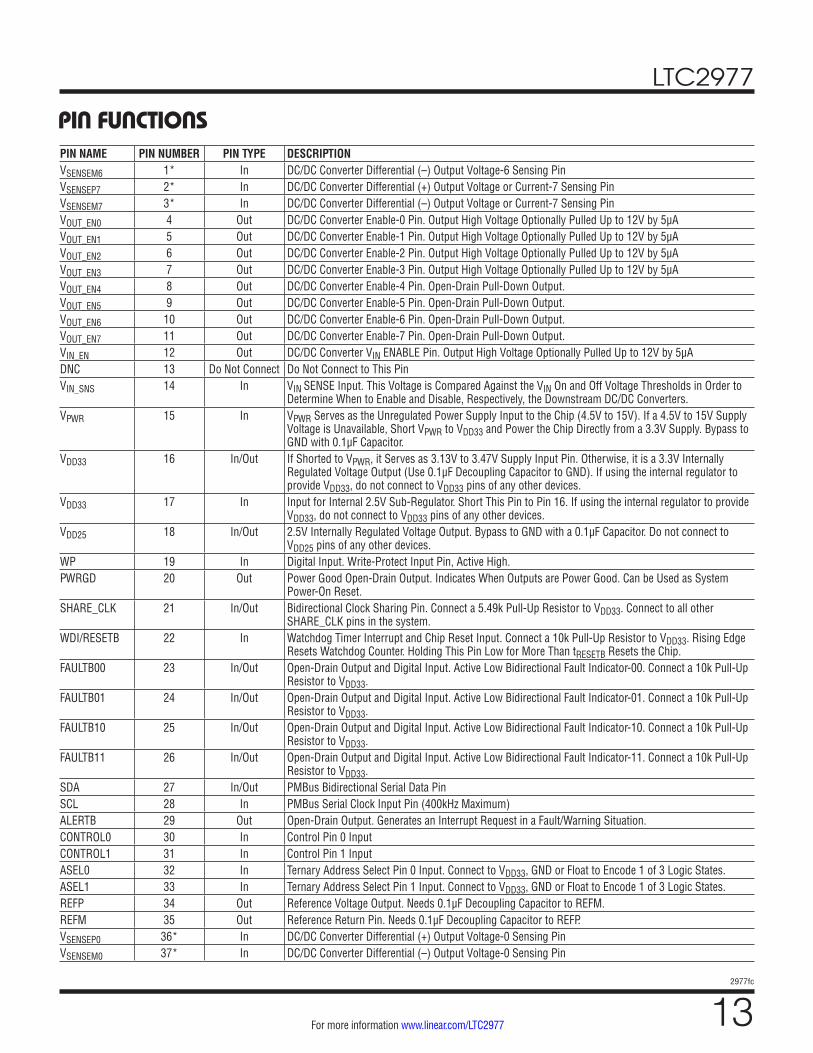
PIN FUNCTIONSPIN NAME PIN NUMBER PIN TYPE DESCRIPTIONVSENSEM6 1* In DC/DC Converter Differential (–) Output Voltage-6 Sensing PinVSENSEP7 2* In DC/DC Converter Differential (+) Output Voltage or Current-7 Sensing PinVSENSEM7 3* In DC/DC Converter Differential (–) Output Voltage or Current-7 Sensing PinVOUT_EN0 4 Out DC/DC Converter Enable-0 Pin. Output High Voltage Optionally Pulled Up to 12V by 5µAVOUT_EN1 5 Out DC/DC Converter Enable-1 Pin. Output High Voltage Optionally Pulled Up to 12V by 5µAVOUT_EN2 6 Out DC/DC Converter Enable-2 Pin. Output High Voltage Optionally Pulled Up to 12V by 5µAVOUT_EN3 7 Out DC/DC Converter Enable-3 Pin. Output High Voltage Optionally Pulled Up to 12V by 5µAVOUT_EN4 8 Out DC/DC Converter Enable-4 Pin. Open-Drain Pull-Down Output.VOUT_EN5 9 Out DC/DC Converter Enable-5 Pin. Open-Drain Pull-Down Output.VOUT_EN6 10 Out DC/DC Converter Enable-6 Pin. Open-Drain Pull-Down Output.VOUT_EN7 11 Out DC/DC Converter Enable-7 Pin. Open-Drain Pull-Down Output.VIN_EN 12 Out DC/DC Converter VIN ENABLE Pin. Output High Voltage Optionally Pulled Up to 12V by 5µADNC 13 Do Not Connect Do Not Connect to This PinVIN_SNS 14 In VIN SENSE Input. This Voltage is Compared Against the VIN On and Off Voltage Thresholds in Order to
Determine When to Enable and Disable, Respectively, the Downstream DC/DC Converters.VPWR 15 In VPWR Serves as the Unregulated Power Supply Input to the Chip (4.5V to 15V). If a 4.5V to 15V Supply
Voltage is Unavailable, Short VPWR to VDD33 and Power the Chip Directly from a 3.3V Supply. Bypass to GND with 0.1µF Capacitor.
VDD33 16 In/Out If Shorted to VPWR, it Serves as 3.13V to 3.47V Supply Input Pin. Otherwise, it is a 3.3V Internally Regulated Voltage Output (Use 0.1µF Decoupling Capacitor to GND). If using the internal regulator to provide VDD33, do not connect to VDD33 pins of any other devices.
VDD33 17 In Input for Internal 2.5V Sub-Regulator. Short This Pin to Pin 16. If using the internal regulator to provide VDD33, do not connect to VDD33 pins of any other devices.
VDD25 18 In/Out 2.5V Internally Regulated Voltage Output. Bypass to GND with a 0.1µF Capacitor. Do not connect to VDD25 pins of any other devices.
WP 19 In Digital Input. Write-Protect Input Pin, Active High.PWRGD 20 Out Power Good Open-Drain Output. Indicates When Outputs are Power Good. Can be Used as System
Power-On Reset.SHARE_CLK 21 In/Out Bidirectional Clock Sharing Pin. Connect a 5.49k Pull-Up Resistor to VDD33. Connect to all other
SHARE_CLK pins in the system.WDI/RESETB 22 In Watchdog Timer Interrupt and Chip Reset Input. Connect a 10k Pull-Up Resistor to VDD33. Rising Edge
Resets Watchdog Counter. Holding This Pin Low for More Than tRESETB Resets the Chip.FAULTB00 23 In/Out Open-Drain Output and Digital Input. Active Low Bidirectional Fault Indicator-00. Connect a 10k Pull-Up
Resistor to VDD33.FAULTB01 24 In/Out Open-Drain Output and Digital Input. Active Low Bidirectional Fault Indicator-01. Connect a 10k Pull-Up
Resistor to VDD33.FAULTB10 25 In/Out Open-Drain Output and Digital Input. Active Low Bidirectional Fault Indicator-10. Connect a 10k Pull-Up
Resistor to VDD33.FAULTB11 26 In/Out Open-Drain Output and Digital Input. Active Low Bidirectional Fault Indicator-11. Connect a 10k Pull-Up
Resistor to VDD33.SDA 27 In/Out PMBus Bidirectional Serial Data PinSCL 28 In PMBus Serial Clock Input Pin (400kHz Maximum)ALERTB 29 Out Open-Drain Output. Generates an Interrupt Request in a Fault/Warning Situation.CONTROL0 30 In Control Pin 0 InputCONTROL1 31 In Control Pin 1 InputASEL0 32 In Ternary Address Select Pin 0 Input. Connect to VDD33, GND or Float to Encode 1 of 3 Logic States.ASEL1 33 In Ternary Address Select Pin 1 Input. Connect to VDD33, GND or Float to Encode 1 of 3 Logic States.REFP 34 Out Reference Voltage Output. Needs 0.1µF Decoupling Capacitor to REFM.REFM 35 Out Reference Return Pin. Needs 0.1µF Decoupling Capacitor to REFP.VSENSEP0 36* In DC/DC Converter Differential (+) Output Voltage-0 Sensing PinVSENSEM0 37* In DC/DC Converter Differential (–) Output Voltage-0 Sensing Pin
LTC2977
142977fc
For more information www.linear.com/LTC2977
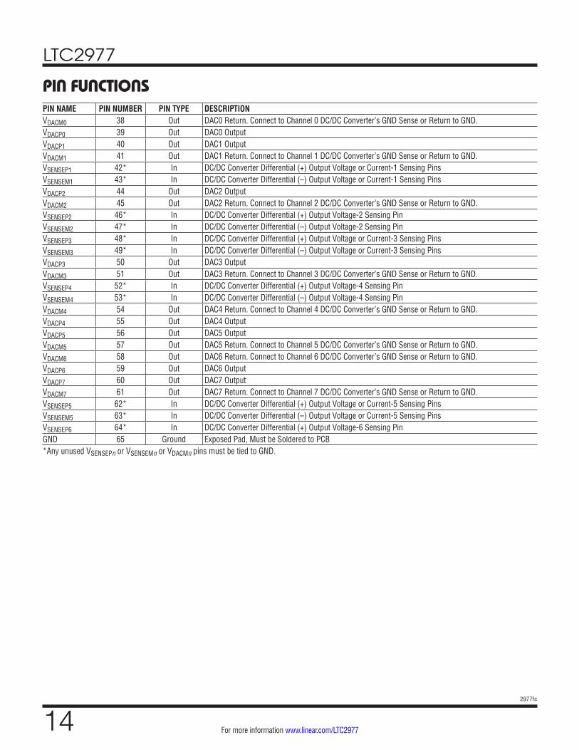
PIN NAME PIN NUMBER PIN TYPE DESCRIPTIONVDACM0 38 Out DAC0 Return. Connect to Channel 0 DC/DC Converter’s GND Sense or Return to GND.VDACP0 39 Out DAC0 OutputVDACP1 40 Out DAC1 OutputVDACM1 41 Out DAC1 Return. Connect to Channel 1 DC/DC Converter’s GND Sense or Return to GND.VSENSEP1 42* In DC/DC Converter Differential (+) Output Voltage or Current-1 Sensing PinsVSENSEM1 43* In DC/DC Converter Differential (–) Output Voltage or Current-1 Sensing PinsVDACP2 44 Out DAC2 OutputVDACM2 45 Out DAC2 Return. Connect to Channel 2 DC/DC Converter’s GND Sense or Return to GND.VSENSEP2 46* In DC/DC Converter Differential (+) Output Voltage-2 Sensing PinVSENSEM2 47* In DC/DC Converter Differential (–) Output Voltage-2 Sensing PinVSENSEP3 48* In DC/DC Converter Differential (+) Output Voltage or Current-3 Sensing PinsVSENSEM3 49* In DC/DC Converter Differential (–) Output Voltage or Current-3 Sensing PinsVDACP3 50 Out DAC3 OutputVDACM3 51 Out DAC3 Return. Connect to Channel 3 DC/DC Converter’s GND Sense or Return to GND.VSENSEP4 52* In DC/DC Converter Differential (+) Output Voltage-4 Sensing PinVSENSEM4 53* In DC/DC Converter Differential (–) Output Voltage-4 Sensing PinVDACM4 54 Out DAC4 Return. Connect to Channel 4 DC/DC Converter’s GND Sense or Return to GND.VDACP4 55 Out DAC4 OutputVDACP5 56 Out DAC5 OutputVDACM5 57 Out DAC5 Return. Connect to Channel 5 DC/DC Converter’s GND Sense or Return to GND.VDACM6 58 Out DAC6 Return. Connect to Channel 6 DC/DC Converter’s GND Sense or Return to GND.VDACP6 59 Out DAC6 OutputVDACP7 60 Out DAC7 OutputVDACM7 61 Out DAC7 Return. Connect to Channel 7 DC/DC Converter’s GND Sense or Return to GND.VSENSEP5 62* In DC/DC Converter Differential (+) Output Voltage or Current-5 Sensing PinsVSENSEM5 63* In DC/DC Converter Differential (–) Output Voltage or Current-5 Sensing PinsVSENSEP6 64* In DC/DC Converter Differential (+) Output Voltage-6 Sensing PinGND 65 Ground Exposed Pad, Must be Soldered to PCB*Any unused VSENSEPn or VSENSEMn or VDACMn pins must be tied to GND.
PIN FUNCTIONS
LTC2977
152977fc
For more information www.linear.com/LTC2977
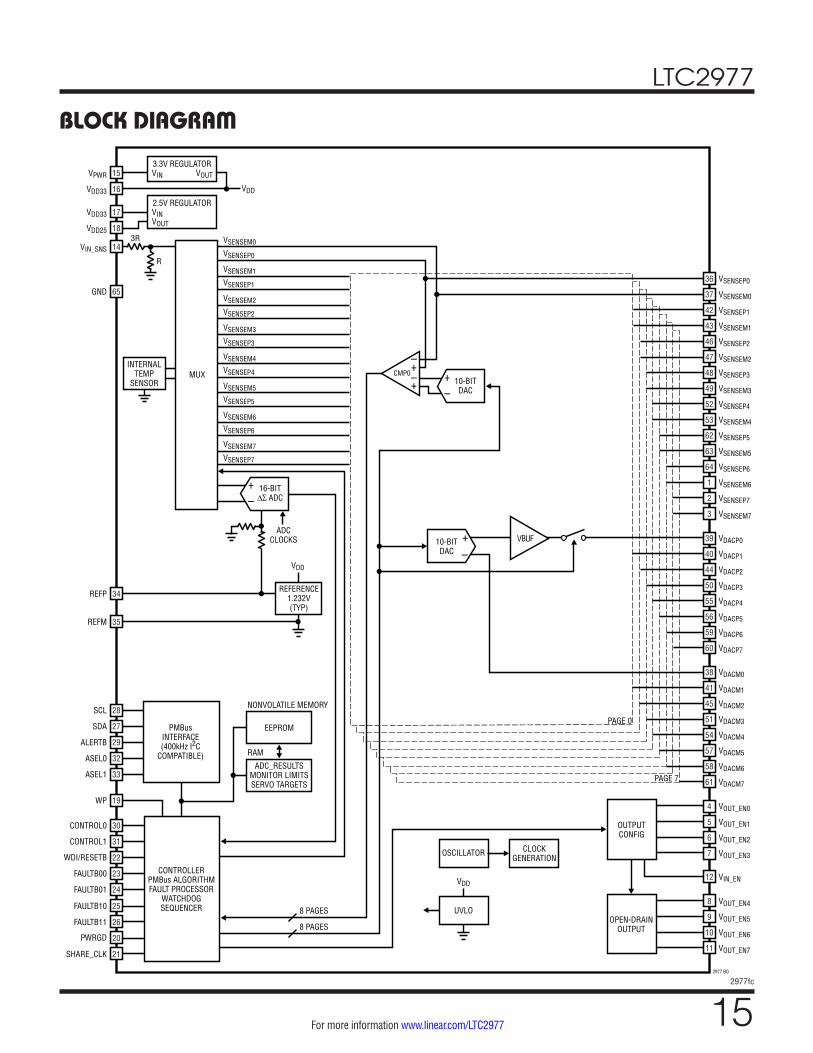
BLOCK DIAGRAM
153.3V REGULATOR
INTERNALTEMP
SENSOR
REFERENCE1.232V(TYP)
OUTPUTCONFIG
CLOCKGENERATION
OSCILLATOR
UVLO
VDD
8 PAGESOPEN-DRAIN
OUTPUT
EEPROM
NONVOLATILE MEMORY
RAM
ADC_RESULTSMONITOR LIMITSSERVO TARGETS
PMBusINTERFACE(400kHz I2C
COMPATIBLE)
CONTROLLERPMBus ALGORITHMFAULT PROCESSOR
WATCHDOGSEQUENCER
VIN
VDD
VSENSEM0
VSENSEP0
VOUTVPWR
172.5V REGULATORVINVOUT
VDD33
36 VSENSEP0
37 VSENSEM0
VSENSEP1
VSENSEM1
VSENSEP2
VSENSEM2
VSENSEP3
VSENSEM3
VSENSEP4
VSENSEM4
VSENSEP5
VSENSEM5
VSENSEP6
VSENSEM6
2 VSENSEP7
3 VSENSEM7
VDACP1
VDACP2
VDACP3
VDACP4
VDACP5
VDACP6
VDACP7
VDACM1
VDACM2
VDACM3
VDACM4
VDACM5
VDACM6
VDACM7PAGE 7
PAGE 0
4 VOUT_EN0
5 VOUT_EN1
6 VOUT_EN2
7 VOUT_EN3
8 VOUT_EN4
9 VOUT_EN5
10 VOUT_EN6
11 VOUT_EN7
2977 BD
12 VIN_EN
18VDD25
65GND
28SCL
27SDA
29ALERTB
32ASEL0
33ASEL1
30CONTROL0
19WP
31CONTROL1
WDI/RESETB 22
23FAULTB00
24FAULTB01
25FAULTB10
26FAULTB11
20
21SHARE_CLK
PWRGD
16VDD33
14VIN_SNS
REFP
REFM
3R
RVSENSEM1
VSENSEP1
VSENSEM2
VSENSEP2
VSENSEM3
VSENSEP3
VSENSEM4
VSENSEP4
VSENSEM5
VSENSEP5
VSENSEM6
VSENSEP6
VSENSEM7
VSENSEP7
16-BIT∆∑ ADC
ADCCLOCKS
VDD
+–
+–
MUX
34
35
10-BITDAC
+
+
–
–CMP0
42
43
46
47
48
49
52
53
62
63
64
1
40
44
50
55
56
60
41
45
51
54
57
58
61
59
VBUF10-BITDAC
+–
VDACM038
VDACP039
8 PAGES
LTC2977
162977fc
For more information www.linear.com/LTC2977
OPERATIONOPERATION OVERVIEW
The LTC2977 is a PMBus programmable power system controller, monitor, sequencer and voltage supervisor that can perform the following operations:n Accept PMBus compatible programming commands.n Provide DC/DC converter input voltage and output volt-
age/current readback through the PMBus interface.n Control the output of DC/DC converters that set the
output voltage with a trim pin or DC/DC converters that set the output voltage using an external resistor feedback network.
n Sequence the start-up of DC/DC converters via PMBus programming and their control input pins. Time-based sequencing and tracking sequencing are both supported.
n Trim the DC/DC converter output voltage (typically in 0.02% steps), in closed-loop servo operating mode, through PMBus programming.
n Margin the DC/DC converter output voltage to PMBus programmed limits.
n Allow the user to trim or margin the DC/DC converter output voltage in a manual operating mode by providing direct access to the margin DAC.
n Supervise the DC/DC converter output voltage, input voltage, and the LTC2977 die temperature for over-value/undervalue conditions with respect to PMBus programmed limits and generate appropriate faults and warnings.
n Respond to a fault condition by either continuing op-eration indefinitely, latching off after a programmable deglitch period, latching off immediately or sequenc-ing off after TOFF_DELAY. A retry mode may be used to automatically recover from a latched-off condition. When enabled, the number of retries (0 to 6 or infi-nite) is the same for all pages and is programmed in MFR_RETRY_COUNT.
n Optionally stop trimming the DC/DC converter output voltage after reaching the initial margin or nominal target. Optionally allow servo to resume if target drifts outside of VOUT warning limits.
n Store command register contents to EEPROM with CRC and ECC through PMBus programming.
n Restore EEPROM contents through PMBus program-ming or when VDD33 is applied on power-up.
n Report the DC/DC converter output voltage status through the PMBus interface and the power good output.
n Generate interrupt requests by asserting the ALERTB pin in response to supported PMBus faults and warnings.
n Coordinate system wide fault responses for all DC/DC converters connected to the FAULTBz0 and FAULTBz1 pins.
n Synchronize sequencing delays or shutdown for multiple devices using the SHARE_CLK pin.
n Software and hardware write protect the command registers.
n Disable the input voltage to the supervised DC/DC converters in response to output voltage OV and UV faults.
n Log telemetry and status data to EEPROM in response to a faulted-off condition
n Supervise an external microcontroller’s activity for a stalled condition with a programmable watchdog timer and reset it if necessary.
n Prevent a DC/DC converter from re-entering the ON state after a power cycle until a programmable interval (MFR_RESTART_DELAY) has elapsed and its output has decayed below a programmable threshold voltage (MFR_VOUT_DISCHARGE_THRESHOLD).
n Record minimum and maximum observed values of input voltage, output voltages and temperature.
n Access user EEPROM data directly, without altering RAM space (MFR_EE_UNLOCK, MFR_EE_ERASE, and MFR_EE_DATA). Facilitates in-house bulk program-ming.
LTC2977
172977fc
For more information www.linear.com/LTC2977
OPERATIONEEPROM
The LTC2977 contains internal EEPROM (nonvolatile memory) with error-correcting code (ECC) to store con-figuration settings and fault log information. EEPROM endurance, retention, and mass write operation time are specified over the operating junction temperature range. See Electrical Characteristics and Absolute Maximum Ratings sections.
Nondestructive operation above TJ = 105°C is possible although the Electrical Characteristics are not guaranteed and the EEPROM will be degraded.
Operating the EEPROM above 105°C may result in a degradation of retention characteristics. The fault logging function, which is useful in debugging system problems that may occur at high temperatures, only writes to fault log EEPROM locations. If occasional writes to these registers occur above 105°C, a slight degradation in the data retention characteristics of the fault log may occur.
It is recommended that the EEPROM not be written using STORE_USER_ALL or bulk programming when TJ > 85°C.
The degradation in EEPROM retention for temperatures >105°C can be approximated by calculating the dimen-sionless acceleration factor using the following equation.
AF = e
Eak
• 1
TUSE + 273− 1
TSTRESS + 273
where:
AF = acceleration factor
Ea = activation energy = 1.4 eV
k = 8.617 × 10⁻⁵ eV/°K
TUSE = 105°C specified junction temperature
TSTRESS = actual junction temperature °C
Example: Calculate the effect on retention when operating at a junction temperature of 125°C for 10 hours.
TSTRESS = 125°C
TUSE = 105°C
AF = 8.65
Equivalent operating time at 105°C = 86.5 hours.
So the overall retention of the EEPROM was degraded by 76.5 hours as a result of operation at a junction tempera-ture of 125°C for 10 hours. Note that the effect of this overstress is negligible when compared to the overall EEPROM retention rating of 175,200 hours at a maximum junction temperature of 105°C.
RESET
Holding the WDI/RESETB pin low for more than tRESETB will cause the LTC2977 to enter the power-on reset state. While in the power-on reset state, the device will not communicate on the I2C bus. Following the subsequent rising-edge of the WDI/RESETB pin, the LTC2977 will execute its power-on sequence per the user configuration stored in EEPROM. Connect WDI/RESETB to VDD33 with a 10k resistor. WDI/RESETB includes an internal 256µs deglitch filter so additional filter capacitance on this pin is not recommended.
OTHER OPERATIONS
Clock Sharing
Multiple LTC PMBus devices can synchronize their clocks in an application by connecting together the open-drain SHARE_CLK input/outputs to a pull-up resistor as a wired OR. In this case the fastest clock will take over and syn-chronize all LTC2977s.
SHARE_CLK can optionally be used to synchronize ON/OFF dependency on VIN across multiple chips by set-ting the Mfr_config_all_vin_share_enable bit of the MFR_CONFIG_ALL_LTC2977 register. When configured this way the chip will hold SHARE_CLK low when the unit is off for insufficient input voltage and upon detecting that SHARE_CLK is held low the chip will disable all channels after a brief deglitch period. When the SHARE_CLK pin is allowed to rise, the chip will respond by beginning a soft-start sequence. In this case the slowest VIN_ON detection will take over and synchronize other chips to its soft-start sequence.
LTC2977
182977fc
For more information www.linear.com/LTC2977
PMBus SERIAL DIGITAL INTERFACE
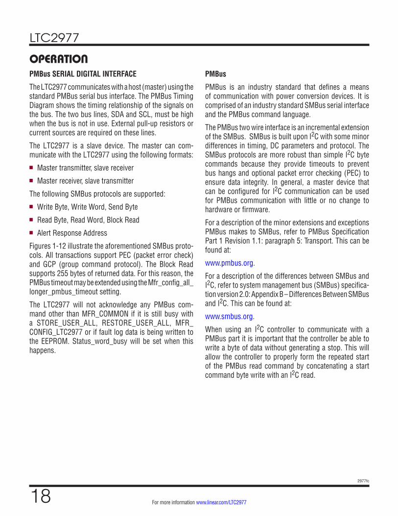
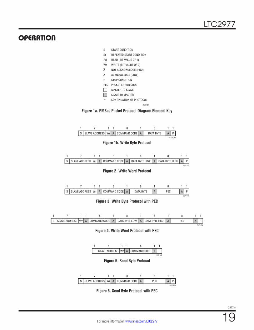
The LTC2977 communicates with a host (master) using the standard PMBus serial bus interface. The PMBus Timing Diagram shows the timing relationship of the signals on the bus. The two bus lines, SDA and SCL, must be high when the bus is not in use. External pull-up resistors or current sources are required on these lines.
The LTC2977 is a slave device. The master can com-municate with the LTC2977 using the following formats:n Master transmitter, slave receivern Master receiver, slave transmitter
The following SMBus protocols are supported:n Write Byte, Write Word, Send Byten Read Byte, Read Word, Block Readn Alert Response Address
Figures 1-12 illustrate the aforementioned SMBus proto-cols. All transactions support PEC (packet error check) and GCP (group command protocol). The Block Read supports 255 bytes of returned data. For this reason, the PMBus timeout may be extended using the Mfr_config_all_ longer_pmbus_timeout setting.
The LTC2977 will not acknowledge any PMBus com-mand other than MFR_COMMON if it is still busy with a STORE_USER_ALL, RESTORE_USER_ALL, MFR_CONFIG_LTC2977 or if fault log data is being written to the EEPROM. Status_word_busy will be set when this happens.
PMBus
PMBus is an industry standard that defines a means of communication with power conversion devices. It is comprised of an industry standard SMBus serial interface and the PMBus command language.
The PMBus two wire interface is an incremental extension of the SMBus. SMBus is built upon I2C with some minor differences in timing, DC parameters and protocol. The SMBus protocols are more robust than simple I2C byte commands because they provide timeouts to prevent bus hangs and optional packet error checking (PEC) to ensure data integrity. In general, a master device that can be configured for I2C communication can be used for PMBus communication with little or no change to hardware or firmware.
For a description of the minor extensions and exceptions PMBus makes to SMBus, refer to PMBus Specification Part 1 Revision 1.1: paragraph 5: Transport. This can be found at:
www.pmbus.org.
For a description of the differences between SMBus and I2C, refer to system management bus (SMBus) specifica-tion version 2.0: Appendix B – Differences Between SMBus and I2C. This can be found at:
www.smbus.org.
When using an I2C controller to communicate with a PMBus part it is important that the controller be able to write a byte of data without generating a stop. This will allow the controller to properly form the repeated start of the PMBus read command by concatenating a start command byte write with an I2C read.
OPERATION
LTC2977
192977fc
For more information www.linear.com/LTC2977
OPERATION
SLAVE ADDRESS COMMAND CODE DATA BYTE LOWWr A A A P2977 F02
S
7 8 8 1
DATA BYTE HIGH
81 1 1 1 11
A
SLAVE ADDRESS COMMAND CODE DATA BYTEWr A A A P2977 F03
S
7 8 8 1
PEC
81 1 1 1 11
A
SLAVE ADDRESS COMMAND CODE DATA BYTE LOWWr A A A P2977 F04
S
7 8 8 1
DATA BYTE HIGH
8
PEC
811 1 1 1 11
A A
Figure 1b. Write Byte Protocol
Figure 2. Write Word Protocol
Figure 3. Write Byte Protocol with PEC
Figure 4. Write Word Protocol with PEC
SLAVE ADDRESS Wr A A P2977 F05
S
7 81 1 1 11
COMMAND CODE
SLAVE ADDRESS COMMAND CODE PECWr A A A P2977 F06
S
7 8 81 1 1 1 11
Figure 5. Send Byte Protocol
Figure 6. Send Byte Protocol with PEC
Figure 1a. PMBus Packet Protocol Diagram Element Key
SLAVE ADDRESS COMMAND CODE DATA BYTEWr A A A P2977 F01b
S
7 8 81 1 1 1 11
2977 F01a
S
Sr
Rd
Wr
A
A
P
PEC
...
START CONDITION
REPEATED START CONDITION
READ (BIT VALUE OF 1)
WRITE (BIT VALUE OF 0)
NOT ACKNOWLEDGE (HIGH)
ACKNOWLEDGE (LOW)
STOP CONDITION
PACKET ERROR CODE
MASTER TO SLAVE
SLAVE TO MASTER
CONTINUATION OF PROTOCOL
LTC2977
202977fc
For more information www.linear.com/LTC2977
OPERATION
Figure 10. Read Byte Protocol with PEC
SLAVE ADDRESS COMMAND CODE SLAVE ADDRESSWr A AS
7 8 7 1
BYTE COUNT = N
8 11 1 1
Sr
11
A
1
Rd A • • •
• • • A P2977 F11
DATA BYTE N
8 1 1
ADATA BYTE 1
8
DATA BYTE 2
81 1
A
A P2977 F12
PEC
8 1 1
SLAVE ADDRESS COMMAND CODE SLAVE ADDRESSWr A AS
7 8 7 1
BYTE COUNT = N
8 11 1 1
Sr
11
A
1
Rd A • • •
• • • ADATA BYTE N
8 1
ADATA BYTE 1
8
DATA BYTE 2
81 1
A
Figure 11. Block Read
Figure 12. Block Read with PEC
SLAVE ADDRESS COMMAND CODE SLAVE ADDRESSWr A A A P2977 F07
S
7 8 7 1
DATA BYTE LOW
8
DATA BYTE HIGH
811 1 1
Sr
1 1 11
A
1
Rd A
SLAVE ADDRESS COMMAND CODE SLAVE ADDRESSWr A A A PA2977 F08
S
7 8 7 1
DATA BYTE LOW
8
DATA BYTE HIGH PEC
8 811 1 1 1 111
Sr
1
A
1
Rd A
Figure 7. Read Word Protocol
Figure 8. Read Word Protocol with PEC
Figure 9. Read Byte Protocol
SLAVE ADDRESS COMMAND CODE SLAVE ADDRESSWr A A Sr P2977 F09
S
7 8 7 11
DATA BYTE
8 11 1 1 11 1
ARd A
SLAVE ADDRESS COMMAND CODE SLAVE ADDRESSWr A A Sr P2977 F10
S
7 8 7 11
DATA BYTE
8 11 1 1 11 1
ARd A
1
A PEC
LTC2977
212977fc
For more information www.linear.com/LTC2977
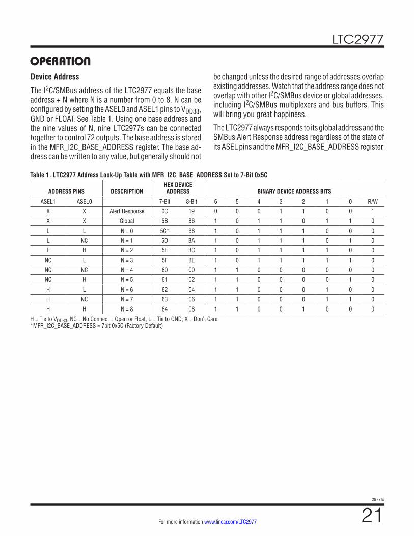
Device Address
The I2C/SMBus address of the LTC2977 equals the base address + N where N is a number from 0 to 8. N can be configured by setting the ASEL0 and ASEL1 pins to VDD33, GND or FLOAT. See Table 1. Using one base address and the nine values of N, nine LTC2977s can be connected together to control 72 outputs. The base address is stored in the MFR_I2C_BASE_ADDRESS register. The base ad-dress can be written to any value, but generally should not
Table 1. LTC2977 Address Look-Up Table with MFR_I2C_BASE_ADDRESS Set to 7-Bit 0x5C
ADDRESS PINS DESCRIPTIONHEX DEVICE ADDRESS BINARY DEVICE ADDRESS BITS
ASEL1 ASEL0 7-Bit 8-Bit 6 5 4 3 2 1 0 R/W
X X Alert Response 0C 19 0 0 0 1 1 0 0 1
X X Global 5B B6 1 0 1 1 0 1 1 0
L L N = 0 5C* B8 1 0 1 1 1 0 0 0
L NC N = 1 5D BA 1 0 1 1 1 0 1 0
L H N = 2 5E BC 1 0 1 1 1 1 0 0
NC L N = 3 5F BE 1 0 1 1 1 1 1 0
NC NC N = 4 60 C0 1 1 0 0 0 0 0 0
NC H N = 5 61 C2 1 1 0 0 0 0 1 0
H L N = 6 62 C4 1 1 0 0 0 1 0 0
H NC N = 7 63 C6 1 1 0 0 0 1 1 0
H H N = 8 64 C8 1 1 0 0 1 0 0 0
H = Tie to VDD33, NC = No Connect = Open or Float, L = Tie to GND, X = Don’t Care *MFR_I2C_BASE_ADDRESS = 7bit 0x5C (Factory Default)
be changed unless the desired range of addresses overlap existing addresses. Watch that the address range does not overlap with other I2C/SMBus device or global addresses, including I2C/SMBus multiplexers and bus buffers. This will bring you great happiness.
The LTC2977 always responds to its global address and the SMBus Alert Response address regardless of the state of its ASEL pins and the MFR_I2C_BASE_ADDRESS register.
OPERATION
LTC2977
222977fc
For more information www.linear.com/LTC2977
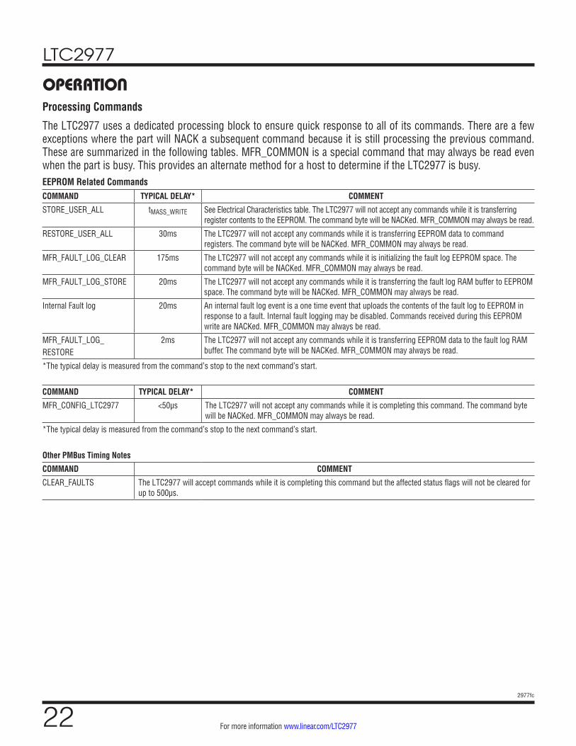
Processing Commands
The LTC2977 uses a dedicated processing block to ensure quick response to all of its commands. There are a few exceptions where the part will NACK a subsequent command because it is still processing the previous command. These are summarized in the following tables. MFR_COMMON is a special command that may always be read even when the part is busy. This provides an alternate method for a host to determine if the LTC2977 is busy.EEPROM Related CommandsCOMMAND TYPICAL DELAY* COMMENT
STORE_USER_ALL tMASS_WRITE See Electrical Characteristics table. The LTC2977 will not accept any commands while it is transferring register contents to the EEPROM. The command byte will be NACKed. MFR_COMMON may always be read.
RESTORE_USER_ALL 30ms The LTC2977 will not accept any commands while it is transferring EEPROM data to command registers. The command byte will be NACKed. MFR_COMMON may always be read.
MFR_FAULT_LOG_CLEAR 175ms The LTC2977 will not accept any commands while it is initializing the fault log EEPROM space. The command byte will be NACKed. MFR_COMMON may always be read.
MFR_FAULT_LOG_STORE 20ms The LTC2977 will not accept any commands while it is transferring the fault log RAM buffer to EEPROM space. The command byte will be NACKed. MFR_COMMON may always be read.
Internal Fault log 20ms An internal fault log event is a one time event that uploads the contents of the fault log to EEPROM in response to a fault. Internal fault logging may be disabled. Commands received during this EEPROM write are NACKed. MFR_COMMON may always be read.
MFR_FAULT_LOG_RESTORE
2ms The LTC2977 will not accept any commands while it is transferring EEPROM data to the fault log RAM buffer. The command byte will be NACKed. MFR_COMMON may always be read.
*The typical delay is measured from the command’s stop to the next command’s start.
COMMAND TYPICAL DELAY* COMMENT
MFR_CONFIG_LTC2977 <50µs The LTC2977 will not accept any commands while it is completing this command. The command byte will be NACKed. MFR_COMMON may always be read.
*The typical delay is measured from the command’s stop to the next command’s start.
Other PMBus Timing Notes
COMMAND COMMENT
CLEAR_FAULTS The LTC2977 will accept commands while it is completing this command but the affected status flags will not be cleared for up to 500µs.
OPERATION
LTC2977
232977fc
For more information www.linear.com/LTC2977
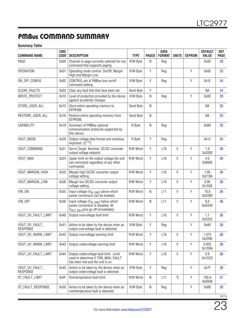
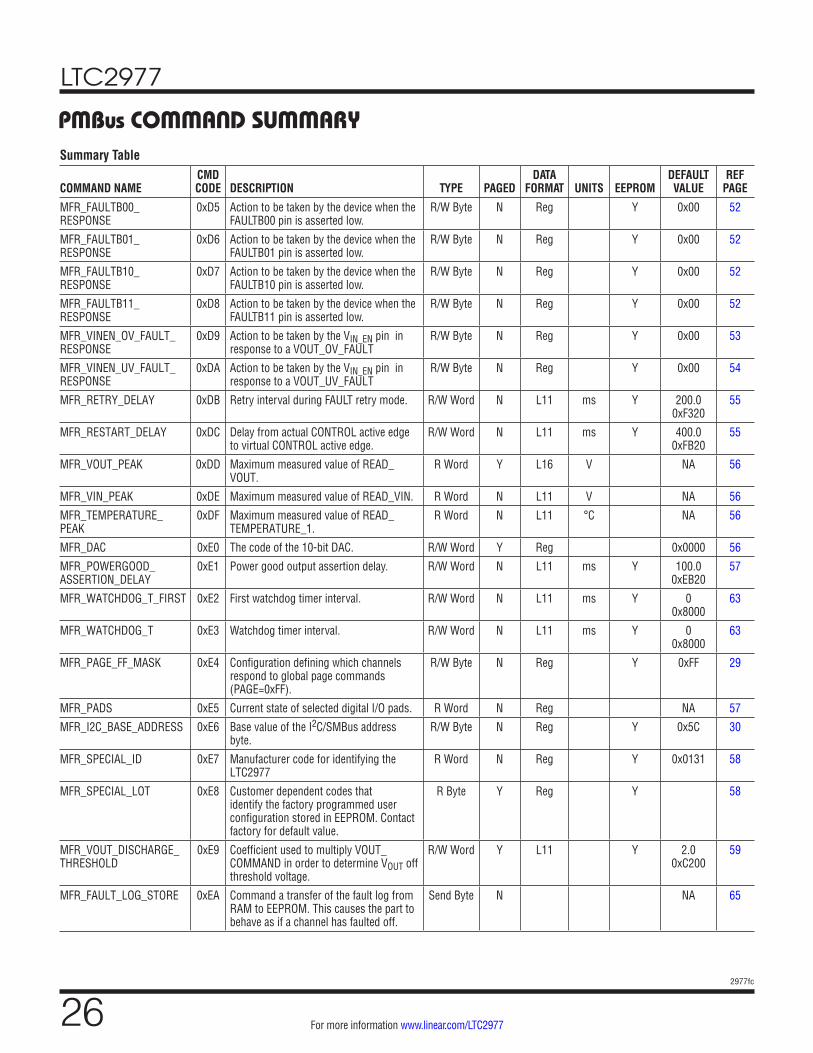
PMBus COMMAND SUMMARYSummary Table
COMMAND NAMECMD CODE DESCRIPTION TYPE PAGED
DATA FORMAT UNITS EEPROM
DEFAULT VALUE
REF PAGE
PAGE 0x00 Channel or page currently selected for any command that supports paging.
R/W Byte N Reg 0x00 28
OPERATION 0x01 Operating mode control. On/Off, Margin High and Margin Low.
R/W Byte Y Reg Y 0x00 33
ON_OFF_CONFIG 0x02 CONTROL pin & PMBus bus on/off command setting.
R/W Byte Y Reg Y 0x1E 34
CLEAR_FAULTS 0x03 Clear any fault bits that have been set. Send Byte Y NA 34
WRITE_PROTECT 0x10 Level of protection provided by the device against accidental changes.
R/W Byte N Reg Y 0x00 28
STORE_USER_ALL 0x15 Store entire operating memory to EEPROM.
Send Byte N NA 35
RESTORE_USER_ALL 0x16 Restore entire operating memory from EEPROM.
Send Byte N NA 35
CAPABILITY 0x19 Summary of PMBus optional communication protocols supported by this device.
R Byte N Reg 0xB0 35
VOUT_MODE 0x20 Output voltage data format and mantissa exponent. (2–13)
R Byte Y Reg 0x13 35
VOUT_COMMAND 0x21 Servo Target. Nominal DC/DC converter output voltage setpoint.
R/W Word Y L16 V Y 1.0 0x2000
36
VOUT_MAX 0x24 Upper limit on the output voltage the unit can command regardless of any other commands.
R/W Word Y L16 V Y 4.0 0x8000
36
VOUT_MARGIN_HIGH 0x25 Margin high DC/DC converter output voltage setting.
R/W Word Y L16 V Y 1.05 0x219A
36
VOUT_MARGIN_LOW 0x26 Margin low DC/DC converter output voltage setting.
R/W Word Y L16 V Y 0.95 0x1E66
36
VIN_ON 0x35 Input voltage (VIN_SNS) above which power conversion can be enabled.
R/W Word N L11 V Y 10.0 0xD280
36
VIN_OFF 0x36 Input voltage (VIN_SNS) below which power conversion is disabled. All VOUT_ENn pins go off immediately.
R/W Word N L11 V Y 9.0 0xD240
36
VOUT_OV_FAULT_LIMIT 0x40 Output overvoltage fault limit R/W Word Y L16 V Y 1.1 0x2333
36
VOUT_OV_FAULT_RESPONSE
0x41 Action to be taken by the device when an output overvoltage fault is detected.
R/W Byte Y Reg Y 0x80 38
VOUT_OV_WARN_LIMIT 0x42 Output overvoltage warning limit . R/W Word Y L16 V Y 1.075 0x2266
36
VOUT_UV_WARN_LIMIT 0x43 Output undervoltage warning limit R/W Word Y L16 V Y 0.925 0x1D9A
36
VOUT_UV_FAULT_LIMIT 0x44 Output undervoltage fault limit. Limit used to determine if TON_MAX_FAULT has been met and the unit is on.
R/W Word Y L16 V Y 0.9 0x1CCD
36
VOUT_UV_FAULT_RESPONSE
0x45 Action to be taken by the device when an output undervoltage fault is detected.
R/W Byte Y Reg Y 0x7F 38
OT_FAULT_LIMIT 0x4F Overtemperature fault limit. R/W Word N L11 °C Y 105.0 0xEB48
37
OT_FAULT_RESPONSE 0x50 Action to be taken by the device when an overtemperature fault is detected.
R/W Byte N Reg Y 0xB8 39

LTC2977
242977fc
For more information www.linear.com/LTC2977
PMBus COMMAND SUMMARYSummary Table
COMMAND NAMECMD CODE DESCRIPTION TYPE PAGED
DATA FORMAT UNITS EEPROM
DEFAULT VALUE
REF PAGE
OT_WARN_LIMIT 0x51 Overtemperature warning limit. R/W Word N L11 °C Y 70.0 0xEA30
37
UT_WARN_LIMIT 0x52 Undertemperature warning limit. R/W Word N L11 °C Y 0 0x8000
37
UT_FAULT_LIMIT 0x53 Undertemperature fault limit. R/W Word N L11 °C Y –40.0 0xE580
37
UT_FAULT_RESPONSE 0x54 Action to be taken by the device when an undertemperature fault is detected.
R/W Byte N Reg Y 0xB8 39
VIN_OV_FAULT_LIMIT 0x55 Input overvoltage fault limit measured at VIN_SNS pin
R/W Word N L11 V Y 15.0 0xD3C0
36
VIN_OV_FAULT_RESPONSE
0x56 Action to be taken by the device when an input overvoltage fault is detected.
R/W Byte N Reg Y 0x80 39
VIN_OV_WARN_LIMIT 0x57 Input overvoltage warning limit measured at VIN_SNS pin
R/W Word N L11 V Y 14.0 0xD380
36
VIN_UV_WARN_LIMIT 0x58 Input undervoltage warning limit measured at VIN_SNS pin.
R/W Word N L11 V Y 0 0x8000
36
VIN_UV_FAULT_LIMIT 0x59 Input undervoltage fault limit measured at VIN_SNS pin
R/W Word N L11 V Y 0 0x8000
36
VIN_UV_FAULT_RESPONSE
0x5A Action to be taken by the device when an input undervoltage fault is detected.
R/W Byte N Reg Y 0x00 39
POWER_GOOD_ON 0x5E Output voltage at or above which a power good should be asserted.
R/W Word Y L16 V Y 0.96 0x1EB8
36
POWER_GOOD_OFF 0x5F Output voltage at or below which a power good should be deasserted.
R/W Word Y L16 V Y 0.94 0x1E14
36
TON_DELAY 0x60 Time from CONTROL pin and/or OPERATION command = ON to VOUT_ENn pin = ON.
R/W Word Y L11 ms Y 1.0 0xBA00
37
TON_RISE 0x61 Time from when the VOUT_ENn pin goes high until the LTC2977 optionally soft-connects its DAC and begins to servo the output voltage to the desired value.
R/W Word Y L11 ms Y 10.0 0xD280
37
TON_MAX_FAULT_LIMIT 0x62 Maximum time from VOUT_ENn = ON assertion that an UV condition will be tolerated before a TON_MAX_FAULT condition results.
R/W Word Y L11 ms Y 15.0 0xD3C0
37
TON_MAX_FAULT_RESPONSE
0x63 Action to be taken by the device when a TON_MAX_FAULT event is detected.
R/W Byte Y Reg Y 0xB8 40
TOFF_DELAY 0x64 Time from CONTROL pin and/or OPERATION command = OFF to VOUT_ENn pin = OFF.
R/W Word Y L11 ms Y 1.0 0xBA00
37
STATUS_BYTE 0x78 One byte summary of the unit’s fault condition.
R Byte Y Reg NA 41
STATUS_WORD 0x79 Two byte summary of the unit’s fault condition.
R Word Y Reg NA 41
STATUS_VOUT 0x7A Output voltage fault and warning status. R Byte Y Reg NA 42
STATUS_INPUT 0x7C Input voltage fault and warning status measured at VIN_SNS pin.
R Byte N Reg NA 42
STATUS_TEMPERATURE 0x7D Temperature fault and warning status for READ_TEMPERATURE_1.
R Byte N Reg NA 42
LTC2977
252977fc
For more information www.linear.com/LTC2977
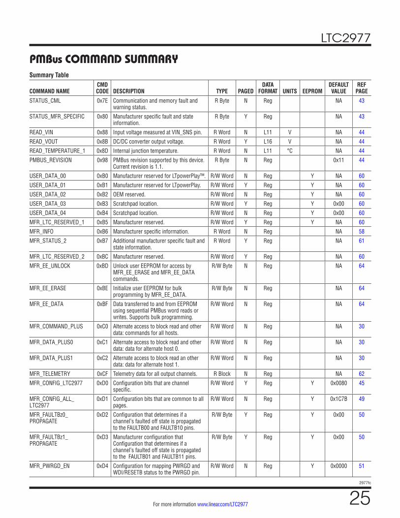
PMBus COMMAND SUMMARYSummary Table
COMMAND NAMECMD CODE DESCRIPTION TYPE PAGED
DATA FORMAT UNITS EEPROM
DEFAULT VALUE
REF PAGE
STATUS_CML 0x7E Communication and memory fault and warning status.
R Byte N Reg NA 43
STATUS_MFR_SPECIFIC 0x80 Manufacturer specific fault and state information.
R Byte Y Reg NA 43
READ_VIN 0x88 Input voltage measured at VIN_SNS pin. R Word N L11 V NA 44
READ_VOUT 0x8B DC/DC converter output voltage. R Word Y L16 V NA 44
READ_TEMPERATURE_1 0x8D Internal junction temperature. R Word N L11 °C NA 44
PMBUS_REVISION 0x98 PMBus revision supported by this device. Current revision is 1.1.
R Byte N Reg 0x11 44
USER_DATA_00 0xB0 Manufacturer reserved for LTpowerPlay™. R/W Word N Reg Y NA 60
USER_DATA_01 0xB1 Manufacturer reserved for LTpowerPlay. R/W Word Y Reg Y NA 60
USER_DATA_02 0xB2 OEM reserved. R/W Word N Reg Y NA 60
USER_DATA_03 0xB3 Scratchpad location. R/W Word Y Reg Y 0x00 60
USER_DATA_04 0xB4 Scratchpad location. R/W Word N Reg Y 0x00 60
MFR_LTC_RESERVED_1 0xB5 Manufacturer reserved. R/W Word Y Reg Y NA 60
MFR_INFO 0xB6 Manufacturer specific information. R Word N Reg NA 58
MFR_STATUS_2 0xB7 Additional manufacturer specific fault and state information.
R Word Y Reg NA 61
MFR_LTC_RESERVED_2 0xBC Manufacturer reserved. R/W Word Y Reg NA 60
MFR_EE_UNLOCK 0xBD Unlock user EEPROM for access by MFR_EE_ERASE and MFR_EE_DATA commands.
R/W Byte N Reg NA 64
MFR_EE_ERASE 0xBE Initialize user EEPROM for bulk programming by MFR_EE_DATA.
R/W Byte N Reg NA 64
MFR_EE_DATA 0xBF Data transferred to and from EEPROM using sequential PMBus word reads or writes. Supports bulk programming.
R/W Word N Reg NA 64
MFR_COMMAND_PLUS 0xC0 Alternate access to block read and other data: commands for all hosts.
R/W Word N Reg NA 30
MFR_DATA_PLUS0 0xC1 Alternate access to block read and other data: data for alternate host 0.
R/W Word N Reg NA 30
MFR_DATA_PLUS1 0xC2 Alternate access to block read an other data: data for alternate host 1.
R/W Word N Reg NA 30
MFR_TELEMETRY 0xCF Telemetry data for all output channels. R Block N Reg NA 62
MFR_CONFIG_LTC2977 0xD0 Configuration bits that are channel specific.
R/W Word Y Reg Y 0x0080 45
MFR_CONFIG_ALL_LTC2977
0xD1 Configuration bits that are common to all pages.
R/W Word N Reg Y 0x1C7B 49
MFR_FAULTBz0_PROPAGATE
0xD2 Configuration that determines if a channel’s faulted off state is propagated to the FAULTB00 and FAULTB10 pins.
R/W Byte Y Reg Y 0x00 50
MFR_FAULTBz1_PROPAGATE
0xD3 Manufacturer configuration that Configuration that determines if a channel’s faulted off state is propagated to the FAULTB01 and FAULTB11 pins.
R/W Byte Y Reg Y 0x00 50
MFR_PWRGD_EN 0xD4 Configuration for mapping PWRGD and WDI/RESETB status to the PWRGD pin.
R/W Word N Reg Y 0x0000 51
LTC2977
262977fc
For more information www.linear.com/LTC2977
PMBus COMMAND SUMMARYSummary Table
COMMAND NAMECMD CODE DESCRIPTION TYPE PAGED
DATA FORMAT UNITS EEPROM
DEFAULT VALUE
REF PAGE
MFR_FAULTB00_RESPONSE
0xD5 Action to be taken by the device when the FAULTB00 pin is asserted low.
R/W Byte N Reg Y 0x00 52
MFR_FAULTB01_RESPONSE
0xD6 Action to be taken by the device when the FAULTB01 pin is asserted low.
R/W Byte N Reg Y 0x00 52
MFR_FAULTB10_RESPONSE
0xD7 Action to be taken by the device when the FAULTB10 pin is asserted low.
R/W Byte N Reg Y 0x00 52
MFR_FAULTB11_RESPONSE
0xD8 Action to be taken by the device when the FAULTB11 pin is asserted low.
R/W Byte N Reg Y 0x00 52
MFR_VINEN_OV_FAULT_RESPONSE
0xD9 Action to be taken by the VIN_EN pin in response to a VOUT_OV_FAULT
R/W Byte N Reg Y 0x00 53
MFR_VINEN_UV_FAULT_RESPONSE
0xDA Action to be taken by the VIN_EN pin in response to a VOUT_UV_FAULT
R/W Byte N Reg Y 0x00 54
MFR_RETRY_DELAY 0xDB Retry interval during FAULT retry mode. R/W Word N L11 ms Y 200.0 0xF320
55
MFR_RESTART_DELAY 0xDC Delay from actual CONTROL active edge to virtual CONTROL active edge.
R/W Word N L11 ms Y 400.0 0xFB20
55
MFR_VOUT_PEAK 0xDD Maximum measured value of READ_VOUT.
R Word Y L16 V NA 56
MFR_VIN_PEAK 0xDE Maximum measured value of READ_VIN. R Word N L11 V NA 56
MFR_TEMPERATURE_PEAK
0xDF Maximum measured value of READ_TEMPERATURE_1.
R Word N L11 °C NA 56
MFR_DAC 0xE0 The code of the 10-bit DAC. R/W Word Y Reg 0x0000 56
MFR_POWERGOOD_ASSERTION_DELAY
0xE1 Power good output assertion delay. R/W Word N L11 ms Y 100.0 0xEB20
57
MFR_WATCHDOG_T_FIRST 0xE2 First watchdog timer interval. R/W Word N L11 ms Y 0 0x8000
63
MFR_WATCHDOG_T 0xE3 Watchdog timer interval. R/W Word N L11 ms Y 0 0x8000
63
MFR_PAGE_FF_MASK 0xE4 Configuration defining which channels respond to global page commands (PAGE=0xFF).
R/W Byte N Reg Y 0xFF 29
MFR_PADS 0xE5 Current state of selected digital I/O pads. R Word N Reg NA 57
MFR_I2C_BASE_ADDRESS 0xE6 Base value of the I2C/SMBus address byte.
R/W Byte N Reg Y 0x5C 30
MFR_SPECIAL_ID 0xE7 Manufacturer code for identifying the LTC2977
R Word N Reg Y 0x0131 58
MFR_SPECIAL_LOT 0xE8 Customer dependent codes that identify the factory programmed user configuration stored in EEPROM. Contact factory for default value.
R Byte Y Reg Y 58
MFR_VOUT_DISCHARGE_THRESHOLD
0xE9 Coefficient used to multiply VOUT_COMMAND in order to determine VOUT off threshold voltage.
R/W Word Y L11 Y 2.0 0xC200
59
MFR_FAULT_LOG_STORE 0xEA Command a transfer of the fault log from RAM to EEPROM. This causes the part to behave as if a channel has faulted off.
Send Byte N NA 65
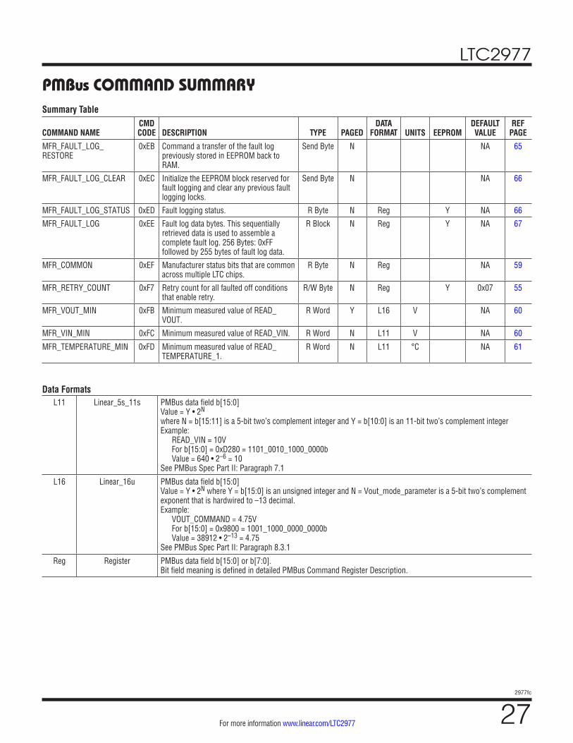
LTC2977
272977fc
For more information www.linear.com/LTC2977
PMBus COMMAND SUMMARYSummary Table
COMMAND NAMECMD CODE DESCRIPTION TYPE PAGED
DATA FORMAT UNITS EEPROM
DEFAULT VALUE
REF PAGE
MFR_FAULT_LOG_RESTORE
0xEB Command a transfer of the fault log previously stored in EEPROM back to RAM.
Send Byte N NA 65
MFR_FAULT_LOG_CLEAR 0xEC Initialize the EEPROM block reserved for fault logging and clear any previous fault logging locks.
Send Byte N NA 66
MFR_FAULT_LOG_STATUS 0xED Fault logging status. R Byte N Reg Y NA 66
MFR_FAULT_LOG 0xEE Fault log data bytes. This sequentially retrieved data is used to assemble a complete fault log. 256 Bytes: 0xFF followed by 255 bytes of fault log data.
R Block N Reg Y NA 67
MFR_COMMON 0xEF Manufacturer status bits that are common across multiple LTC chips.
R Byte N Reg NA 59
MFR_RETRY_COUNT 0xF7 Retry count for all faulted off conditions that enable retry.
R/W Byte N Reg Y 0x07 55
MFR_VOUT_MIN 0xFB Minimum measured value of READ_VOUT.
R Word Y L16 V NA 60
MFR_VIN_MIN 0xFC Minimum measured value of READ_VIN. R Word N L11 V NA 60
MFR_TEMPERATURE_MIN 0xFD Minimum measured value of READ_TEMPERATURE_1.
R Word N L11 °C NA 61
Data FormatsL11 Linear_5s_11s PMBus data field b[15:0]
Value = Y • 2N where N = b[15:11] is a 5-bit two’s complement integer and Y = b[10:0] is an 11-bit two’s complement integer Example: READ_VIN = 10V For b[15:0] = 0xD280 = 1101_0010_1000_0000b Value = 640 • 2–6 = 10 See PMBus Spec Part II: Paragraph 7.1
L16 Linear_16u PMBus data field b[15:0] Value = Y • 2N where Y = b[15:0] is an unsigned integer and N = Vout_mode_parameter is a 5-bit two’s complement exponent that is hardwired to –13 decimal. Example: VOUT_COMMAND = 4.75V For b[15:0] = 0x9800 = 1001_1000_0000_0000b Value = 38912 • 2–13 = 4.75 See PMBus Spec Part II: Paragraph 8.3.1
Reg Register PMBus data field b[15:0] or b[7:0]. Bit field meaning is defined in detailed PMBus Command Register Description.
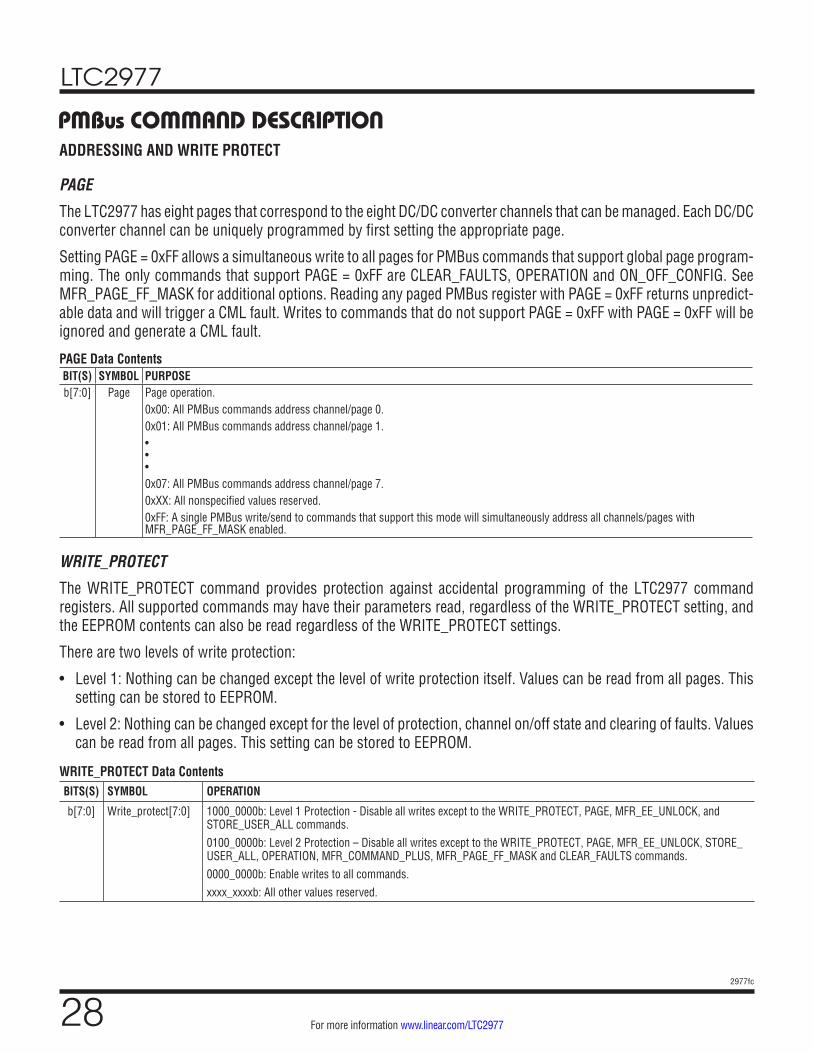
LTC2977
282977fc
For more information www.linear.com/LTC2977
ADDRESSING AND WRITE PROTECT
PAGE
The LTC2977 has eight pages that correspond to the eight DC/DC converter channels that can be managed. Each DC/DC converter channel can be uniquely programmed by first setting the appropriate page.
Setting PAGE = 0xFF allows a simultaneous write to all pages for PMBus commands that support global page program-ming. The only commands that support PAGE = 0xFF are CLEAR_FAULTS, OPERATION and ON_OFF_CONFIG. See MFR_PAGE_FF_MASK for additional options. Reading any paged PMBus register with PAGE = 0xFF returns unpredict-able data and will trigger a CML fault. Writes to commands that do not support PAGE = 0xFF with PAGE = 0xFF will be ignored and generate a CML fault.
PAGE Data ContentsBIT(S) SYMBOL PURPOSEb[7:0] Page Page operation.
0x00: All PMBus commands address channel/page 0. 0x01: All PMBus commands address channel/page 1. • • •0x07: All PMBus commands address channel/page 7. 0xXX: All nonspecified values reserved.0xFF: A single PMBus write/send to commands that support this mode will simultaneously address all channels/pages with MFR_PAGE_FF_MASK enabled.
WRITE_PROTECT
The WRITE_PROTECT command provides protection against accidental programming of the LTC2977 command registers. All supported commands may have their parameters read, regardless of the WRITE_PROTECT setting, and the EEPROM contents can also be read regardless of the WRITE_PROTECT settings.
There are two levels of write protection:
• Level 1: Nothing can be changed except the level of write protection itself. Values can be read from all pages. This setting can be stored to EEPROM.
• Level 2: Nothing can be changed except for the level of protection, channel on/off state and clearing of faults. Values can be read from all pages. This setting can be stored to EEPROM.
WRITE_PROTECT Data ContentsBITS(S) SYMBOL OPERATION
b[7:0] Write_protect[7:0] 1000_0000b: Level 1 Protection - Disable all writes except to the WRITE_PROTECT, PAGE, MFR_EE_UNLOCK, and STORE_USER_ALL commands.0100_0000b: Level 2 Protection – Disable all writes except to the WRITE_PROTECT, PAGE, MFR_EE_UNLOCK, STORE_USER_ALL, OPERATION, MFR_COMMAND_PLUS, MFR_PAGE_FF_MASK and CLEAR_FAULTS commands.0000_0000b: Enable writes to all commands.xxxx_xxxxb: All other values reserved.
PMBus COMMAND DESCRIPTION
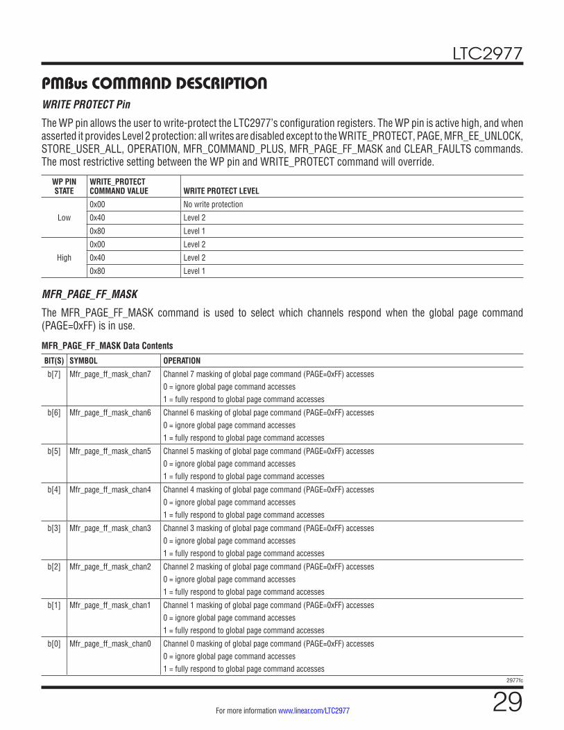
LTC2977
292977fc
For more information www.linear.com/LTC2977
PMBus COMMAND DESCRIPTIONWRITE PROTECT Pin
The WP pin allows the user to write-protect the LTC2977’s configuration registers. The WP pin is active high, and when asserted it provides Level 2 protection: all writes are disabled except to the WRITE_PROTECT, PAGE, MFR_EE_UNLOCK, STORE_USER_ALL, OPERATION, MFR_COMMAND_PLUS, MFR_PAGE_FF_MASK and CLEAR_FAULTS commands. The most restrictive setting between the WP pin and WRITE_PROTECT command will override.
WP PIN STATE
WRITE_PROTECT COMMAND VALUE WRITE PROTECT LEVEL
Low
0x00 No write protection
0x40 Level 2
0x80 Level 1
High
0x00 Level 2
0x40 Level 2
0x80 Level 1
MFR_PAGE_FF_MASK
The MFR_PAGE_FF_MASK command is used to select which channels respond when the global page command (PAGE=0xFF) is in use.
MFR_PAGE_FF_MASK Data Contents
BIT(S) SYMBOL OPERATION
b[7] Mfr_page_ff_mask_chan7 Channel 7 masking of global page command (PAGE=0xFF) accesses0 = ignore global page command accesses1 = fully respond to global page command accesses
b[6] Mfr_page_ff_mask_chan6 Channel 6 masking of global page command (PAGE=0xFF) accesses0 = ignore global page command accesses1 = fully respond to global page command accesses
b[5] Mfr_page_ff_mask_chan5 Channel 5 masking of global page command (PAGE=0xFF) accesses0 = ignore global page command accesses1 = fully respond to global page command accesses
b[4] Mfr_page_ff_mask_chan4 Channel 4 masking of global page command (PAGE=0xFF) accesses0 = ignore global page command accesses1 = fully respond to global page command accesses
b[3] Mfr_page_ff_mask_chan3 Channel 3 masking of global page command (PAGE=0xFF) accesses0 = ignore global page command accesses1 = fully respond to global page command accesses
b[2] Mfr_page_ff_mask_chan2 Channel 2 masking of global page command (PAGE=0xFF) accesses0 = ignore global page command accesses1 = fully respond to global page command accesses
b[1] Mfr_page_ff_mask_chan1 Channel 1 masking of global page command (PAGE=0xFF) accesses0 = ignore global page command accesses1 = fully respond to global page command accesses
b[0] Mfr_page_ff_mask_chan0 Channel 0 masking of global page command (PAGE=0xFF) accesses0 = ignore global page command accesses1 = fully respond to global page command accesses
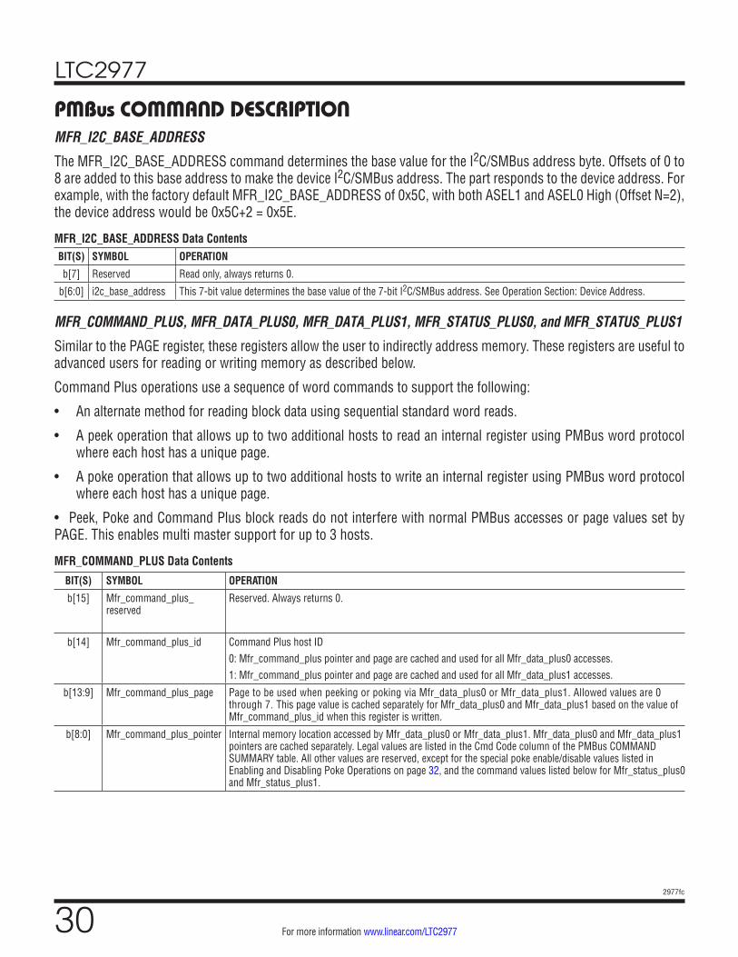
LTC2977
302977fc
For more information www.linear.com/LTC2977
MFR_I2C_BASE_ADDRESS
The MFR_I2C_BASE_ADDRESS command determines the base value for the I2C/SMBus address byte. Offsets of 0 to 8 are added to this base address to make the device I2C/SMBus address. The part responds to the device address. For example, with the factory default MFR_I2C_BASE_ADDRESS of 0x5C, with both ASEL1 and ASEL0 High (Offset N=2), the device address would be 0x5C+2 = 0x5E.
MFR_I2C_BASE_ADDRESS Data ContentsBIT(S) SYMBOL OPERATION
b[7] Reserved Read only, always returns 0.
b[6:0] i2c_base_address This 7-bit value determines the base value of the 7-bit I2C/SMBus address. See Operation Section: Device Address.
MFR_COMMAND_PLUS, MFR_DATA_PLUS0, MFR_DATA_PLUS1, MFR_STATUS_PLUS0, and MFR_STATUS_PLUS1
Similar to the PAGE register, these registers allow the user to indirectly address memory. These registers are useful to advanced users for reading or writing memory as described below.
Command Plus operations use a sequence of word commands to support the following:
• An alternate method for reading block data using sequential standard word reads.
• A peek operation that allows up to two additional hosts to read an internal register using PMBus word protocol where each host has a unique page.
• A poke operation that allows up to two additional hosts to write an internal register using PMBus word protocol where each host has a unique page.
• Peek, Poke and Command Plus block reads do not interfere with normal PMBus accesses or page values set by PAGE. This enables multi master support for up to 3 hosts.
MFR_COMMAND_PLUS Data Contents
BIT(S) SYMBOL OPERATION
b[15] Mfr_command_plus_reserved
Reserved. Always returns 0.
b[14] Mfr_command_plus_id Command Plus host ID0: Mfr_command_plus pointer and page are cached and used for all Mfr_data_plus0 accesses.1: Mfr_command_plus pointer and page are cached and used for all Mfr_data_plus1 accesses.
b[13:9] Mfr_command_plus_page Page to be used when peeking or poking via Mfr_data_plus0 or Mfr_data_plus1. Allowed values are 0 through 7. This page value is cached separately for Mfr_data_plus0 and Mfr_data_plus1 based on the value of Mfr_command_plus_id when this register is written.
b[8:0] Mfr_command_plus_pointer Internal memory location accessed by Mfr_data_plus0 or Mfr_data_plus1. Mfr_data_plus0 and Mfr_data_plus1 pointers are cached separately. Legal values are listed in the Cmd Code column of the PMBus COMMAND SUMMARY table. All other values are reserved, except for the special poke enable/disable values listed in Enabling and Disabling Poke Operations on page 32, and the command values listed below for Mfr_status_plus0 and Mfr_status_plus1.
PMBus COMMAND DESCRIPTION
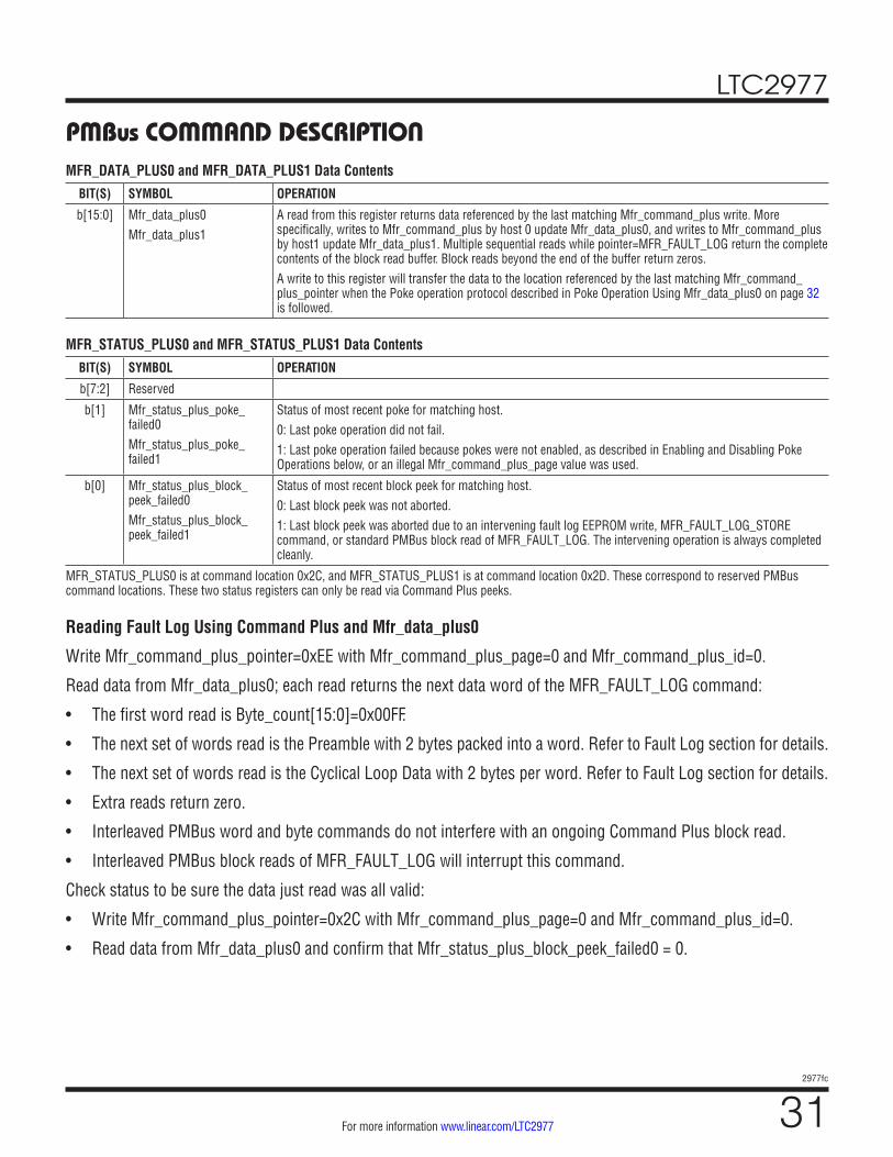
LTC2977
312977fc
For more information www.linear.com/LTC2977
MFR_DATA_PLUS0 and MFR_DATA_PLUS1 Data ContentsBIT(S) SYMBOL OPERATION
b[15:0] Mfr_data_plus0Mfr_data_plus1
A read from this register returns data referenced by the last matching Mfr_command_plus write. More specifically, writes to Mfr_command_plus by host 0 update Mfr_data_plus0, and writes to Mfr_command_plus by host1 update Mfr_data_plus1. Multiple sequential reads while pointer=MFR_FAULT_LOG return the complete contents of the block read buffer. Block reads beyond the end of the buffer return zeros.A write to this register will transfer the data to the location referenced by the last matching Mfr_command_plus_pointer when the Poke operation protocol described in Poke Operation Using Mfr_data_plus0 on page 32 is followed.
MFR_STATUS_PLUS0 and MFR_STATUS_PLUS1 Data ContentsBIT(S) SYMBOL OPERATION
b[7:2] Reserved
b[1] Mfr_status_plus_poke_failed0Mfr_status_plus_poke_failed1
Status of most recent poke for matching host.0: Last poke operation did not fail.1: Last poke operation failed because pokes were not enabled, as described in Enabling and Disabling Poke Operations below, or an illegal Mfr_command_plus_page value was used.
b[0] Mfr_status_plus_block_peek_failed0Mfr_status_plus_block_peek_failed1
Status of most recent block peek for matching host.0: Last block peek was not aborted.1: Last block peek was aborted due to an intervening fault log EEPROM write, MFR_FAULT_LOG_STORE command, or standard PMBus block read of MFR_FAULT_LOG. The intervening operation is always completed cleanly.
MFR_STATUS_PLUS0 is at command location 0x2C, and MFR_STATUS_PLUS1 is at command location 0x2D. These correspond to reserved PMBus command locations. These two status registers can only be read via Command Plus peeks.
Reading Fault Log Using Command Plus and Mfr_data_plus0
Write Mfr_command_plus_pointer=0xEE with Mfr_command_plus_page=0 and Mfr_command_plus_id=0.
Read data from Mfr_data_plus0; each read returns the next data word of the MFR_FAULT_LOG command:
• The first word read is Byte_count[15:0]=0x00FF.
• The next set of words read is the Preamble with 2 bytes packed into a word. Refer to Fault Log section for details.
• The next set of words read is the Cyclical Loop Data with 2 bytes per word. Refer to Fault Log section for details.
• Extra reads return zero.
• Interleaved PMBus word and byte commands do not interfere with an ongoing Command Plus block read.
• Interleaved PMBus block reads of MFR_FAULT_LOG will interrupt this command.
Check status to be sure the data just read was all valid:
• Write Mfr_command_plus_pointer=0x2C with Mfr_command_plus_page=0 and Mfr_command_plus_id=0.
• Read data from Mfr_data_plus0 and confirm that Mfr_status_plus_block_peek_failed0 = 0.
PMBus COMMAND DESCRIPTION
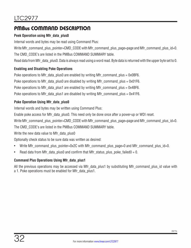
LTC2977
322977fc
For more information www.linear.com/LTC2977
Peek Operation using Mfr_data_plus0
Internal words and bytes may be read using Command Plus:
Write Mfr_command_plus_pointer=CMD_CODE with Mfr_command_plus_page=page and Mfr_command_plus_id=0.
The CMD_CODE’s are listed in the PMBus COMMAND SUMMARY table.
Read data from Mfr_data_plus0. Data is always read using a word read. Byte data is returned with the upper byte set to 0.
Enabling and Disabling Poke Operations
Poke operations to Mfr_data_plus0 are enabled by writing Mfr_command_plus = 0x0BF6.
Poke operations to Mfr_data_plus0 are disabled by writing Mfr_command_plus = 0x01F6.
Poke operations to Mfr_data_plus1 are enabled by writing Mfr_command_plus = 0x4BF6.
Poke operations to Mfr_data_plus1 are disabled by writing Mfr_command_plus = 0x41F6.
Poke Operation Using Mfr_data_plus0
Internal words and bytes may be written using Command Plus:
Enable poke access for Mfr_data_plus0. This need only be done once after a power-up or WDI reset.
Write Mfr_command_plus_pointer=CMD_CODE with Mfr_command_plus_page=page and Mfr_command_plus_id=0.
The CMD_CODE’s are listed in the PMBus COMMAND SUMMARY table.
Write the new data value to Mfr_data_plus0
Optionally check status to be sure data was written as desired:
• Write Mfr_command_plus_pointer=0x2C with Mfr_command_plus_page=0 and Mfr_command_plus_id=0.
• Read data from Mfr_data_plus0 and confirm that Mfr_status_plus_poke_failed0 = 0.
Command Plus Operations Using Mfr_data_plus1
All the previous operations may be accessed via Mfr_data_plus1 by substituting Mfr_command_plus_id value with a 1. Poke operations must be enabled for Mfr_data_plus1.
PMBus COMMAND DESCRIPTION
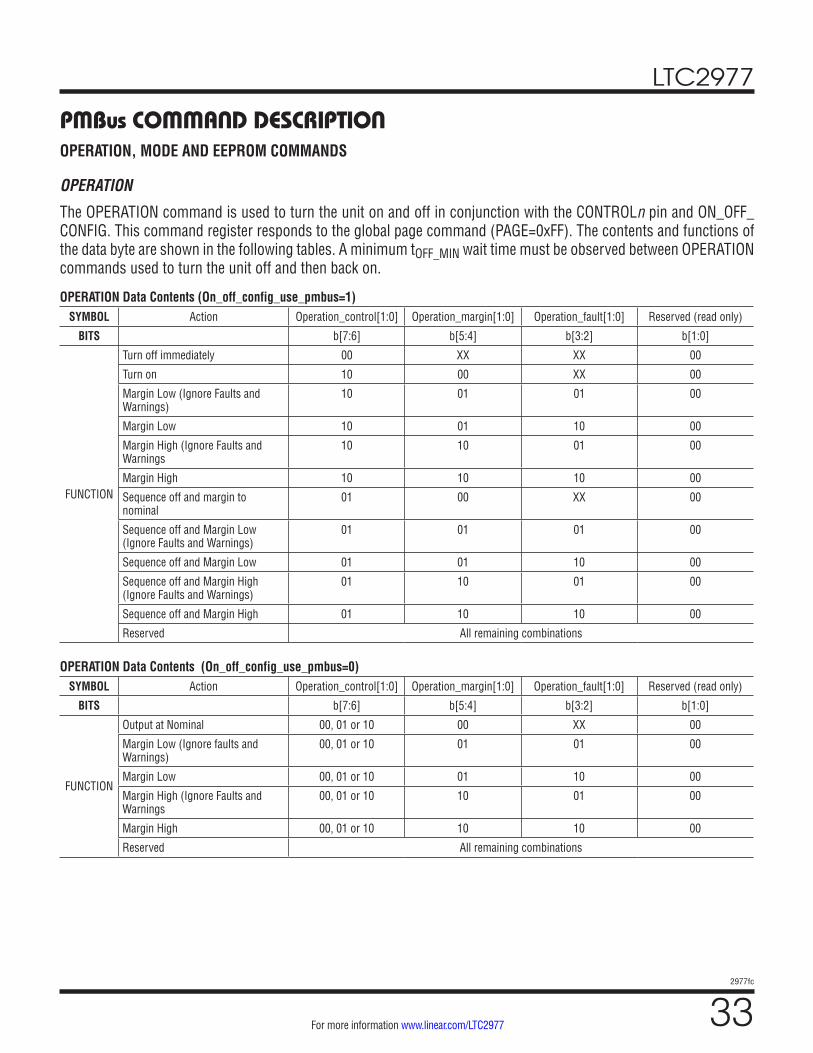
LTC2977
332977fc
For more information www.linear.com/LTC2977
OPERATION, MODE AND EEPROM COMMANDS
OPERATION
The OPERATION command is used to turn the unit on and off in conjunction with the CONTROLn pin and ON_OFF_CONFIG. This command register responds to the global page command (PAGE=0xFF). The contents and functions of the data byte are shown in the following tables. A minimum tOFF_MIN wait time must be observed between OPERATION commands used to turn the unit off and then back on.
OPERATION Data Contents (On_off_config_use_pmbus=1)SYMBOL Action Operation_control[1:0] Operation_margin[1:0] Operation_fault[1:0] Reserved (read only)
BITS b[7:6] b[5:4] b[3:2] b[1:0]
FUNCTION
Turn off immediately 00 XX XX 00
Turn on 10 00 XX 00
Margin Low (Ignore Faults and Warnings)
10 01 01 00
Margin Low 10 01 10 00
Margin High (Ignore Faults and Warnings
10 10 01 00
Margin High 10 10 10 00
Sequence off and margin to nominal
01 00 XX 00
Sequence off and Margin Low (Ignore Faults and Warnings)
01 01 01 00
Sequence off and Margin Low 01 01 10 00
Sequence off and Margin High (Ignore Faults and Warnings)
01 10 01 00
Sequence off and Margin High 01 10 10 00
Reserved All remaining combinations
OPERATION Data Contents (On_off_config_use_pmbus=0)SYMBOL Action Operation_control[1:0] Operation_margin[1:0] Operation_fault[1:0] Reserved (read only)
BITS b[7:6] b[5:4] b[3:2] b[1:0]
FUNCTION
Output at Nominal 00, 01 or 10 00 XX 00
Margin Low (Ignore faults and Warnings)
00, 01 or 10 01 01 00
Margin Low 00, 01 or 10 01 10 00
Margin High (Ignore Faults and Warnings
00, 01 or 10 10 01 00
Margin High 00, 01 or 10 10 10 00
Reserved All remaining combinations
PMBus COMMAND DESCRIPTION
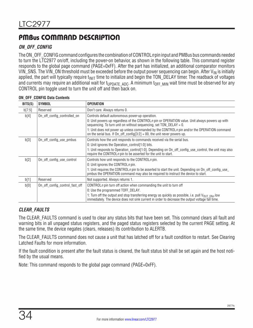
LTC2977
342977fc
For more information www.linear.com/LTC2977
ON_OFF_CONFIG
The ON_OFF_CONFIG command configures the combination of CONTROLn pin input and PMBus bus commands needed to turn the LTC2977 on/off, including the power-on behavior, as shown in the following table. This command register responds to the global page command (PAGE=0xFF). After the part has initialized, an additional comparator monitors VIN_SNS. The VIN_ON threshold must be exceeded before the output power sequencing can begin. After VIN is initially applied, the part will typically require tINIT time to initialize and begin the TON_DELAY timer. The readback of voltages and currents may require an additional wait for tUPDATE_ADC. A minimum tOFF_MIN wait time must be observed for any CONTROL pin toggle used to turn the unit off and then back on.
ON_OFF_CONFIG Data ContentsBITS(S) SYMBOL OPERATION
b[7:5] Reserved Don’t care. Always returns 0.
b[4] On_off_config_controlled_on Controls default autonomous power-up operation.0: Unit powers up regardless of the CONTROLn pin or OPERATION value. Unit always powers up with sequencing. To turn unit on without sequencing, set TON_DELAY = 0.1: Unit does not power up unless commanded by the CONTROLn pin and/or the OPERATION command on the serial bus. If On_off_config[3:2] = 00, the unit never powers up.
b[3] On_off_config_use_pmbus Controls how the unit responds to commands received via the serial bus.0: Unit ignores the Operation_control[1:0] bits.1: Unit responds to Operation_control[1:0]. Depending on On_off_config_use_control, the unit may also require the CONTROLn pin to be asserted for the unit to start.
b[2] On_off_config_use_control Controls how unit responds to the CONTROLn pin. 0: Unit ignores the CONTROLn pin. 1: Unit requires the CONTROLn pin to be asserted to start the unit. Depending on On_off_config_use_pmbus the OPERATION command may also be required to instruct the device to start.
b[1] Reserved Not supported. Always returns 1.
b[0] On_off_config_control_fast_off CONTROLn pin turn off action when commanding the unit to turn off0: Use the programmed TOFF_DELAY. 1: Turn off the output and stop transferring energy as quickly as possible, i.e. pull VOUT_ENn low immediately. The device does not sink current in order to decrease the output voltage fall time.
CLEAR_FAULTS
The CLEAR_FAULTS command is used to clear any status bits that have been set. This command clears all fault and warning bits in all unpaged status registers, and the paged status registers selected by the current PAGE setting. At the same time, the device negates (clears, releases) its contribution to ALERTB.
The CLEAR_FAULTS command does not cause a unit that has latched off for a fault condition to restart. See Clearing Latched Faults for more information.
If the fault condition is present after the fault status is cleared, the fault status bit shall be set again and the host noti-fied by the usual means.
Note: This command responds to the global page command (PAGE=0xFF).
PMBus COMMAND DESCRIPTION
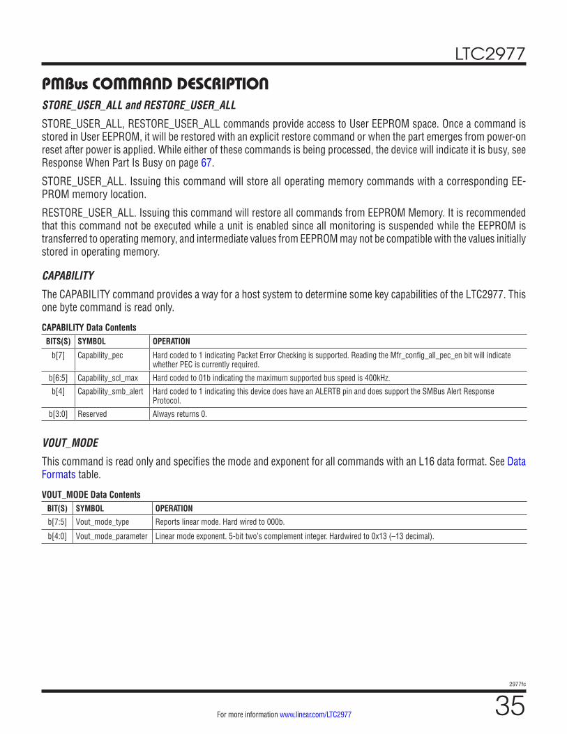
LTC2977
352977fc
For more information www.linear.com/LTC2977
STORE_USER_ALL and RESTORE_USER_ALL
STORE_USER_ALL, RESTORE_USER_ALL commands provide access to User EEPROM space. Once a command is stored in User EEPROM, it will be restored with an explicit restore command or when the part emerges from power-on reset after power is applied. While either of these commands is being processed, the device will indicate it is busy, see Response When Part Is Busy on page 67.
STORE_USER_ALL. Issuing this command will store all operating memory commands with a corresponding EE-PROM memory location.
RESTORE_USER_ALL. Issuing this command will restore all commands from EEPROM Memory. It is recommended that this command not be executed while a unit is enabled since all monitoring is suspended while the EEPROM is transferred to operating memory, and intermediate values from EEPROM may not be compatible with the values initially stored in operating memory.
CAPABILITY
The CAPABILITY command provides a way for a host system to determine some key capabilities of the LTC2977. This one byte command is read only.
CAPABILITY Data ContentsBITS(S) SYMBOL OPERATION
b[7] Capability_pec Hard coded to 1 indicating Packet Error Checking is supported. Reading the Mfr_config_all_pec_en bit will indicate whether PEC is currently required.
b[6:5] Capability_scl_max Hard coded to 01b indicating the maximum supported bus speed is 400kHz.
b[4] Capability_smb_alert Hard coded to 1 indicating this device does have an ALERTB pin and does support the SMBus Alert Response Protocol.
b[3:0] Reserved Always returns 0.
VOUT_MODE
This command is read only and specifies the mode and exponent for all commands with an L16 data format. See Data Formats table.
VOUT_MODE Data ContentsBIT(S) SYMBOL OPERATION
b[7:5] Vout_mode_type Reports linear mode. Hard wired to 000b.
b[4:0] Vout_mode_parameter Linear mode exponent. 5-bit two’s complement integer. Hardwired to 0x13 (–13 decimal).
PMBus COMMAND DESCRIPTION

LTC2977
362977fc
For more information www.linear.com/LTC2977
OUTPUT VOLTAGE RELATED COMMANDS
VOUT_COMMAND, VOUT_MAX, VOUT_MARGIN_HIGH, VOUT_MARGIN_LOW, VOUT_OV_FAULT_LIMIT, VOUT_OV_WARN_LIMIT, VOUT_UV_WARN_LIMIT, VOUT_UV_FAULT_LIMIT, POWER_GOOD_ON and POWER_GOOD_OFF
These commands use the same format and provide various servo, margining, and supervising limits for a channel’s output voltage. When odd channels are configured to measure current, the OV_WARN_LIMIT, UV_WARN_LIMIT, OV_FAULT_LIMIT and UV_FAULT_LIMIT commands are not supported.
Data ContentsBIT(S) SYMBOL OPERATION
b[15:0] Vout_command[15:0],Vout_max[15:0],Vout_margin_high[15:0],Vout_margin_low[15:0],Vout_ov_fault_limit[15:0],Vout_ov_warn_limit[15:0],Vout_uv_warn_limit[15:0],Vout_uv_fault_limit[15:0],Power_good_on[15:0],Power_good_off[15:0]
These commands relate to output voltage. The data uses the L16 format. Units: V
INPUT VOLTAGE RELATED COMMANDS
VIN_ON, VIN_OFF, VIN_OV_FAULT_LIMIT, VIN_OV_WARN_LIMIT, VIN_UV_WARN_LIMIT and VIN_UV_FAULT_LIMIT
These commands use the same format and provide voltage supervising limits for the input voltage VIN_SNS.
Data ContentsBIT(S) SYMBOL OPERATION
b[15:0] Vin_on[15:0],Vin_off[15:0],Vin_ov_fault_limit[15:0],Vin_ov_warn_limit[15:0],Vin_uv_warn_limit[15:0],Vin_uv_fault_limit[15:0]
These commands relate to input voltage. The data uses the L11 format.Units: V.
PMBus COMMAND DESCRIPTION
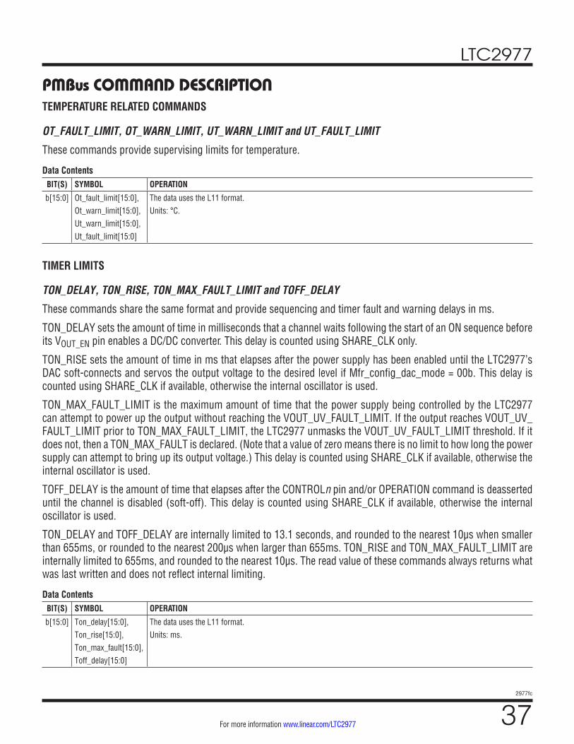
LTC2977
372977fc
For more information www.linear.com/LTC2977
TEMPERATURE RELATED COMMANDS
OT_FAULT_LIMIT, OT_WARN_LIMIT, UT_WARN_LIMIT and UT_FAULT_LIMIT
These commands provide supervising limits for temperature.
Data ContentsBIT(S) SYMBOL OPERATION
b[15:0] Ot_fault_limit[15:0],Ot_warn_limit[15:0],Ut_warn_limit[15:0],Ut_fault_limit[15:0]
The data uses the L11 format.Units: °C.
TIMER LIMITS
TON_DELAY, TON_RISE, TON_MAX_FAULT_LIMIT and TOFF_DELAY
These commands share the same format and provide sequencing and timer fault and warning delays in ms.
TON_DELAY sets the amount of time in milliseconds that a channel waits following the start of an ON sequence before its VOUT_EN pin enables a DC/DC converter. This delay is counted using SHARE_CLK only.
TON_RISE sets the amount of time in ms that elapses after the power supply has been enabled until the LTC2977’s DAC soft-connects and servos the output voltage to the desired level if Mfr_config_dac_mode = 00b. This delay is counted using SHARE_CLK if available, otherwise the internal oscillator is used.
TON_MAX_FAULT_LIMIT is the maximum amount of time that the power supply being controlled by the LTC2977 can attempt to power up the output without reaching the VOUT_UV_FAULT_LIMIT. If the output reaches VOUT_UV_FAULT_LIMIT prior to TON_MAX_FAULT_LIMIT, the LTC2977 unmasks the VOUT_UV_FAULT_LIMIT threshold. If it does not, then a TON_MAX_FAULT is declared. (Note that a value of zero means there is no limit to how long the power supply can attempt to bring up its output voltage.) This delay is counted using SHARE_CLK if available, otherwise the internal oscillator is used.
TOFF_DELAY is the amount of time that elapses after the CONTROLn pin and/or OPERATION command is deasserted until the channel is disabled (soft-off). This delay is counted using SHARE_CLK if available, otherwise the internal oscillator is used.
TON_DELAY and TOFF_DELAY are internally limited to 13.1 seconds, and rounded to the nearest 10µs when smaller than 655ms, or rounded to the nearest 200µs when larger than 655ms. TON_RISE and TON_MAX_FAULT_LIMIT are internally limited to 655ms, and rounded to the nearest 10µs. The read value of these commands always returns what was last written and does not reflect internal limiting.
Data ContentsBIT(S) SYMBOL OPERATION
b[15:0] Ton_delay[15:0],Ton_rise[15:0],Ton_max_fault[15:0],Toff_delay[15:0]
The data uses the L11 format.Units: ms.
PMBus COMMAND DESCRIPTION
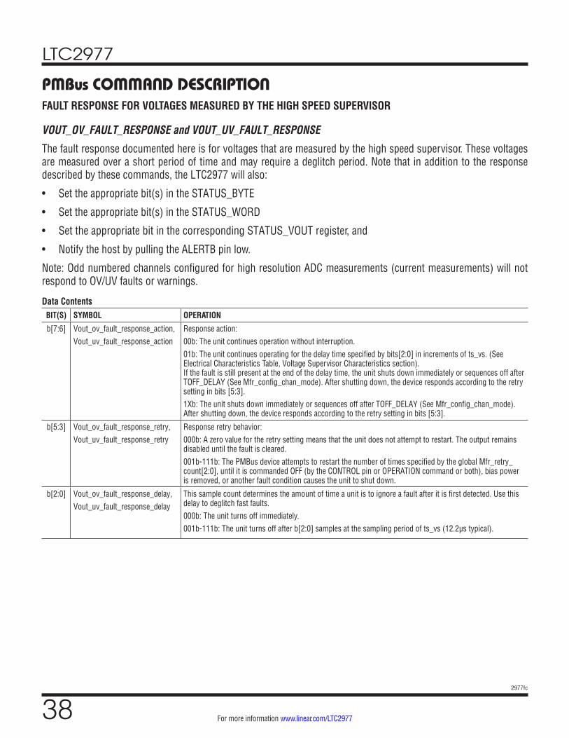
LTC2977
382977fc
For more information www.linear.com/LTC2977
FAULT RESPONSE FOR VOLTAGES MEASURED BY THE HIGH SPEED SUPERVISOR
VOUT_OV_FAULT_RESPONSE and VOUT_UV_FAULT_RESPONSE
The fault response documented here is for voltages that are measured by the high speed supervisor. These voltages are measured over a short period of time and may require a deglitch period. Note that in addition to the response described by these commands, the LTC2977 will also:
• Set the appropriate bit(s) in the STATUS_BYTE
• Set the appropriate bit(s) in the STATUS_WORD
• Set the appropriate bit in the corresponding STATUS_VOUT register, and
• Notify the host by pulling the ALERTB pin low.
Note: Odd numbered channels configured for high resolution ADC measurements (current measurements) will not respond to OV/UV faults or warnings.
Data ContentsBIT(S) SYMBOL OPERATION
b[7:6] Vout_ov_fault_response_action,Vout_uv_fault_response_action
Response action:00b: The unit continues operation without interruption.01b: The unit continues operating for the delay time specified by bits[2:0] in increments of ts_vs. (See Electrical Characteristics Table, Voltage Supervisor Characteristics section). If the fault is still present at the end of the delay time, the unit shuts down immediately or sequences off after TOFF_DELAY (See Mfr_config_chan_mode). After shutting down, the device responds according to the retry setting in bits [5:3].1Xb: The unit shuts down immediately or sequences off after TOFF_DELAY (See Mfr_config_chan_mode). After shutting down, the device responds according to the retry setting in bits [5:3].
b[5:3] Vout_ov_fault_response_retry,Vout_uv_fault_response_retry
Response retry behavior:000b: A zero value for the retry setting means that the unit does not attempt to restart. The output remains disabled until the fault is cleared.001b-111b: The PMBus device attempts to restart the number of times specified by the global Mfr_retry_count[2:0], until it is commanded OFF (by the CONTROL pin or OPERATION command or both), bias power is removed, or another fault condition causes the unit to shut down.
b[2:0] Vout_ov_fault_response_delay,Vout_uv_fault_response_delay
This sample count determines the amount of time a unit is to ignore a fault after it is first detected. Use this delay to deglitch fast faults.000b: The unit turns off immediately.001b-111b: The unit turns off after b[2:0] samples at the sampling period of ts_vs (12.2µs typical).
PMBus COMMAND DESCRIPTION
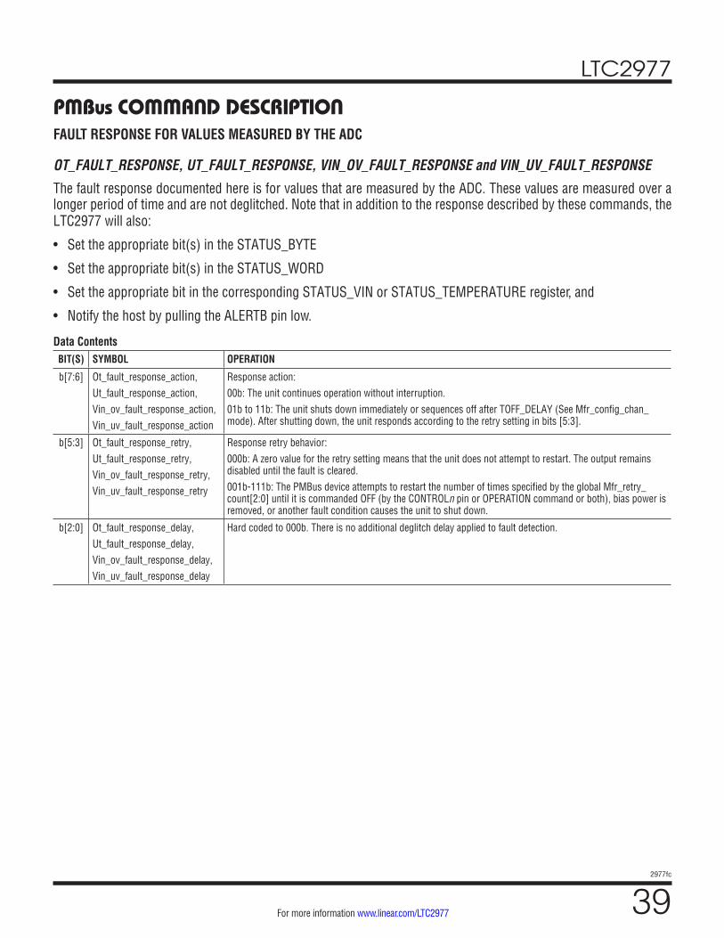
LTC2977
392977fc
For more information www.linear.com/LTC2977
FAULT RESPONSE FOR VALUES MEASURED BY THE ADC
OT_FAULT_RESPONSE, UT_FAULT_RESPONSE, VIN_OV_FAULT_RESPONSE and VIN_UV_FAULT_RESPONSE
The fault response documented here is for values that are measured by the ADC. These values are measured over a longer period of time and are not deglitched. Note that in addition to the response described by these commands, the LTC2977 will also:
• Set the appropriate bit(s) in the STATUS_BYTE
• Set the appropriate bit(s) in the STATUS_WORD
• Set the appropriate bit in the corresponding STATUS_VIN or STATUS_TEMPERATURE register, and
• Notify the host by pulling the ALERTB pin low.
Data ContentsBIT(S) SYMBOL OPERATION
b[7:6] Ot_fault_response_action,Ut_fault_response_action,Vin_ov_fault_response_action,Vin_uv_fault_response_action
Response action: 00b: The unit continues operation without interruption.01b to 11b: The unit shuts down immediately or sequences off after TOFF_DELAY (See Mfr_config_chan_mode). After shutting down, the unit responds according to the retry setting in bits [5:3].
b[5:3] Ot_fault_response_retry,Ut_fault_response_retry,Vin_ov_fault_response_retry,Vin_uv_fault_response_retry
Response retry behavior:000b: A zero value for the retry setting means that the unit does not attempt to restart. The output remains disabled until the fault is cleared.001b-111b: The PMBus device attempts to restart the number of times specified by the global Mfr_retry_count[2:0] until it is commanded OFF (by the CONTROLn pin or OPERATION command or both), bias power is removed, or another fault condition causes the unit to shut down.
b[2:0] Ot_fault_response_delay,Ut_fault_response_delay,Vin_ov_fault_response_delay,Vin_uv_fault_response_delay
Hard coded to 000b. There is no additional deglitch delay applied to fault detection.
PMBus COMMAND DESCRIPTION
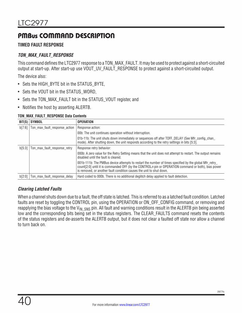
LTC2977
402977fc
For more information www.linear.com/LTC2977
TIMED FAULT RESPONSE
TON_MAX_FAULT_RESPONSE
This command defines the LTC2977 response to a TON_MAX_FAULT. It may be used to protect against a short-circuited output at start-up. After start-up use VOUT_UV_FAULT_RESPONSE to protect against a short-circuited output.
The device also:
• Sets the HIGH_BYTE bit in the STATUS_BYTE,
• Sets the VOUT bit in the STATUS_WORD,
• Sets the TON_MAX_FAULT bit in the STATUS_VOUT register, and
• Notifies the host by asserting ALERTB.
TON_MAX_FAULT_RESPONSE Data ContentsBIT(S) SYMBOL OPERATION
b[7:6] Ton_max_fault_response_action Response action:00b: The unit continues operation without interruption.01b-11b: The unit shuts down immediately or sequences off after TOFF_DELAY (See Mfr_config_chan_mode). After shutting down, the unit responds according to the retry settings in bits [5:3].
b[5:3] Ton_max_fault_response_retry Response retry behavior:000b: A zero value for the Retry Setting means that the unit does not attempt to restart. The output remains disabled until the fault is cleared.001b-111b: The PMBus device attempts to restart the number of times specified by the global Mfr_retry_count[2:0] until it is commanded OFF (by the CONTROLn pin or OPERATION command or both), bias power is removed, or another fault condition causes the unit to shut down.
b[2:0] Ton_max_fault_response_delay Hard coded to 000b. There is no additional deglitch delay applied to fault detection.
Clearing Latched Faults
When a channel shuts down due to a fault, the off state is latched. This is referred to as a latched fault condition. Latched faults are reset by toggling the CONTROL pin, using the OPERATION or ON_OFF_CONFIG command, or removing and reapplying the bias voltage to the VIN_SNS pin. All fault and warning conditions result in the ALERTB pin being asserted low and the corresponding bits being set in the status registers. The CLEAR_FAULTS command resets the contents of the status registers and de-asserts the ALERTB output, but it does not clear a faulted off state nor allow a channel to turn back on.
PMBus COMMAND DESCRIPTION
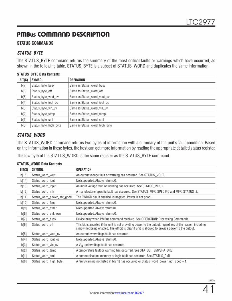
LTC2977
412977fc
For more information www.linear.com/LTC2977
STATUS COMMANDS
STATUS_BYTE
The STATUS_BYTE command returns the summary of the most critical faults or warnings which have occurred, as shown in the following table. STATUS_BYTE is a subset of STATUS_WORD and duplicates the same information.
STATUS_BYTE Data ContentsBIT(S) SYMBOL OPERATION
b[7] Status_byte_busy Same as Status_word_busy
b[6] Status_byte_off Same as Status_word_off
b[5] Status_byte_vout_ov Same as Status_word_vout_ov
b[4] Status_byte_iout_oc Same as Status_word_iout_oc
b[3] Status_byte_vin_uv Same as Status_word_vin_uv
b[2] Status_byte_temp Same as Status_word_temp
b[1] Status_byte_cml Same as Status_word_cml
b[0] Status_byte_high_byte Same as Status_word_high_byte
STATUS_WORD
The STATUS_WORD command returns two bytes of information with a summary of the unit’s fault condition. Based on the information in these bytes, the host can get more information by reading the appropriate detailed status register.
The low byte of the STATUS_WORD is the same register as the STATUS_BYTE command.
STATUS_WORD Data ContentsBIT(S) SYMBOL OPERATION
b[15] Status_word_vout An output voltage fault or warning has occurred. See STATUS_VOUT.
b[14] Status_word_iout Not supported. Always returns 0.
b[13] Status_word_input An input voltage fault or warning has occurred. See STATUS_INPUT.
b[12] Status_word_mfr A manufacturer specific fault has occurred. See STATUS_MFR_SPECIFIC and MFR_STATUS_2.
b[11] Status_word_power_not_good The PWRGD pin, if enabled, is negated. Power is not good.
b[10] Status_word_fans Not supported. Always returns 0.
b[9] Status_word_other Not supported. Always returns 0.
b[8] Status_word_unknown Not supported. Always returns 0.
b[7] Status_word_busy Device busy when PMBus command received. See OPERATION: Processing Commands.
b[6] Status_word_off This bit is asserted if the unit is not providing power to the output, regardless of the reason, including simply not being enabled. The off bit is clear if unit is allowed to provide power to the output.
b[5] Status_word_vout_ov An output overvoltage fault has occurred.
b[4] Status_word_iout_oc Not supported. Always returns 0.
b[3] Status_word_vin_uv A VIN undervoltage fault has occurred.
b[2] Status_word_temp A temperature fault or warning has occurred. See STATUS_TEMPERATURE.
b[1] Status_word_cml A communication, memory or logic fault has occurred. See STATUS_CML.
b[0] Status_word_high_byte A fault/warning not listed in b[7:1] has occurred or Status_word_power_not_good = 1.
PMBus COMMAND DESCRIPTION
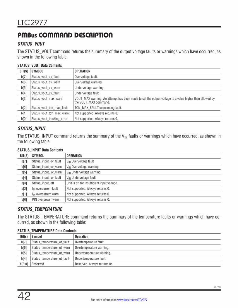
LTC2977
422977fc
For more information www.linear.com/LTC2977
STATUS_VOUT
The STATUS_VOUT command returns the summary of the output voltage faults or warnings which have occurred, as shown in the following table:
STATUS_VOUT Data ContentsBIT(S) SYMBOL OPERATION
b[7] Status_vout_ov_fault Overvoltage fault.
b[6] Status_vout_ov_warn Overvoltage warning.
b[5] Status_vout_uv_warn Undervoltage warning
b[4] Status_vout_uv_fault Undervoltage fault.
b[3] Status_vout_max_warn VOUT_MAX warning. An attempt has been made to set the output voltage to a value higher than allowed by the VOUT_MAX command.
b[2] Status_vout_ton_max_fault TON_MAX_FAULT sequencing fault.
b[1] Status_vout_toff_max_warn Not supported. Always returns 0.
b[0] Status_vout_tracking_error Not supported. Always returns 0.
STATUS_INPUT
The STATUS_INPUT command returns the summary of the VIN faults or warnings which have occurred, as shown in the following table:
STATUS_INPUT Data ContentsBIT(S) SYMBOL OPERATION
b[7] Status_input_ov_fault VIN Overvoltage fault
b[6] Status_input_ov_warn VIN Overvoltage warning
b[5] Status_input_uv_warn VIN Undervoltage warning
b[4] Status_input_uv_fault VIN Undervoltage fault
b[3] Status_input_off Unit is off for insufficient input voltage.
b[2] IIN overcurrent fault Not supported. Always returns 0.
b[1] IIN overcurrent warn Not supported. Always returns 0.
b[0] PIN overpower warn Not supported. Always returns 0.
STATUS_TEMPERATURE
The STATUS_TEMPERATURE command returns the summary of the temperature faults or warnings which have oc-curred, as shown in the following table:
STATUS_TEMPERATURE Data ContentsBit(s) Symbol Operation
b[7] Status_temperature_ot_fault Overtemperature fault.
b[6] Status_temperature_ot_warn Overtemperature warning.
b[5] Status_temperature_ut_warn Undertemperature warning.
b[4] Status_temperature_ut_fault Undertemperature fault.
b[3:0] Reserved Reserved. Always returns 0s.
PMBus COMMAND DESCRIPTION
LTC2977
432977fc
For more information www.linear.com/LTC2977
STATUS_CML
The STATUS_CML command returns the summary of the communication, memory and logic faults or warnings which have occurred, as shown in the following table:
STATUS_CML Data ContentsBIT(S) SYMBOL OPERATION
b[7] Status_cml_cmd_fault Illegal or unsupported command fault has occurred.
b[6] Status_cml_data_fault Illegal or unsupported data received.
b[5] Status_cml_pec_fault A PEC fault has occurred. Note: PEC checking is always active in the LTC2977. Any extra byte received before a STOP will set Status_cml_pec_fault unless the extra byte is a matching PEC byte.
b[4] Status_cml_memory_fault A fault has occurred in the EEPROM.
b[3] Status_cml_processor_fault Not supported, always returns 0.
b[2] Reserved Reserved, always returns 0.
b[1] Status_cml_pmbus_fault A communication fault other than ones listed in this table has occurred. This is a catch all category for illegally formed I2C/SMBus commands (Example: An address byte with read =1 received immediately after a START).
b[0] Status_cml_unknown_fault Not supported, always returns 0.
STATUS_MFR_SPECIFIC
The STATUS_MFR_SPECIFIC command returns manufacturer specific status flags. Bits marked CHANNEL=All are not paged. Bits marked STICKY=Yes stay set until a CLEAR_FAULTS is issued or the channel is commanded on by the user. Bits marked ALERT=Yes pull ALERTB low when the bit is set. Bits marked OFF=Yes indicate that the event can be configured elsewhere to turn the channel off. See MFR_STATUS_2 on page 62 for additional bits related to manufacturer specific status.
STATUS_MFR_SPECIFIC Data ContentsBIT(S) SYMBOL OPERATION CHANNEL STICKY ALERT OFF
b[7] Status_mfr_discharge A VOUT discharge fault occurred while attempting to enter the ON state
Current Page Yes Yes Yes
b[6] Status_mfr_fault1_in This channel attempted to turn on while the FAULTBz1 pin was asserted low, or this channel has shut down at least once in response to a FAULTBz1 pin asserting low since the last CONTROLn pin toggle, OPERATION command ON/OFF cycle or CLEAR_FAULTS command.
Current Page Yes Yes Yes
b[5] Status_mfr_fault0_in This channel attempted to turn on while the FAULTBz0 pin was asserted low, or this channel has shut down at least once in response to a FAULTBz0 pin asserting low since the last CONTROLn pin toggle, OPERATION command ON/OFF cycle or CLEAR_FAULTS command.
Current Page Yes Yes Yes
b[4] Status_mfr_servo_target_reached Servo target has been reached. Current Page No No No
b[3] Status_mfr_dac_connected DAC is connected and driving VDACP pin. Current Page No No No
b[2] Status_mfr_dac_saturated A previous servo operation terminated with maximum or minimum DAC value.
Current Page Yes No No
b[1] Status_mfr_vinen_faulted_off VIN_EN has been deasserted due to a VOUT fault. All No No No
b[0] Status_mfr_watchdog_fault A watchdog fault has occurred. All Yes Yes No
PMBus COMMAND DESCRIPTION
LTC2977
442977fc
For more information www.linear.com/LTC2977
ADC MONITORING COMMANDS
READ_VIN
This command returns the most recent ADC measured value of the voltage measured at the VIN_SNS pin.
READ_VIN Data ContentsBIT(S) SYMBOL OPERATIONb[15:0] Read_vin[15:0] The data uses the L11 format.
Units: V
READ_VOUT
This command returns the most recent ADC measured value of the channel’s output voltage. When odd channels are configured to measure current, the data contents use the L11 format with units in mV.
READ_VOUT Data ContentsBIT(S) SYMBOL OPERATIONb[15:0] Read_vout[15:0] The data uses the L16 format.
Units: V
READ_VOUT Data Contents—for Odd Channels Configured to Measure Current (Mfr_config_adc_hires = 1)Bit(s) Symbol Operation
b[15:0] Read_vout[15:0] The data uses the L11 format.Units: mV
READ_TEMPERATURE_1
This command returns the most recent ADC measured value of junction temperature in °C as determined by the LTC2977’s internal temperature sensor.
READ_TEMPERATURE_1 Data ContentsBIT(S) SYMBOL OPERATION
b[15:0] Read_temperature_1 [15:0] The data uses the L11 format.Units: °C.
PMBUS_REVISION
The PMBUS_REVISION command register is read only and reports the LTC2977 compliance to the PMBus standard revision 1.1.
PMBUS_REVISION Data ContentsBIT(S) SYMBOL OPERATION
b[7:0] PMBus_rev Reports the PMBus standard revision compliance. This is hard-coded to 0x11 for revision 1.1.
PMBus COMMAND DESCRIPTION
LTC2977
452977fc
For more information www.linear.com/LTC2977
MANUFACTURER SPECIFIC COMMANDS
MFR_CONFIG_LTC2977
This command is used to configure various manufacturer specific operating parameters for each channel.
MFR_CONFIG_LTC2977 Data ContentsBIT(S) SYMBOL OPERATION
b[15:14] Mfr_config_chan_mode Select channel specific sequencing mode.00 = Channel uses PMBus delay sequencing with immediate off upon fault.01 = Channel uses PMBus delay sequencing with sequence off upon fault.1x = Channel is a slave in a tracked power supply system.
b[13:12] Reserved Don’t care. Always returns 0.b[11] Mfr_config_fast_servo_off Disables fast servo when margining or trimming output voltages:
0: fast-servo enabled.1: fast-servo disabled.
b[10] Mfr_config_supervisor_resolution Selects supervisor resolution:0: high resolution = 4mV/LSB, range for VVSENSEPn – VVSENSEMn is 0V to 3.8V.1: low resolution = 8mV/LSB, range for VVSENSEPn – VVSENSEMn is 0V to 6.0V.
b[9] Mfr_config_adc_hires Selects ADC resolution for odd channels. This is typically used to measure current. Ignored for even channels (they always use low resolution).0: low resolution = 122µV/LSB.1: high resolution = 15.6µV/LSB.
b[8] Mfr_config_controln_sel Selects the active control pin input (CONTROL0 or CONTROL1) for this channel.0: Select CONTROL0 pin.1: Select CONTROL1 pin.
b[7] Mfr_config_servo_continuous Select whether the UNIT should continuously servo VOUT after it has reached a new margin or nominal target. Only applies when Mfr_config_dac_mode = 00b.0: Do not continuously servo VOUT after reaching initial target.1: Continuously servo VOUT to target.
b[6] Mfr_config_servo_on_warn Control re-servo on warning feature. Only applies when Mfr_config_dac_mode = 00b and Mfr_config_servo_continuous = 0. 0: Do not allow the unit to re-servo when a VOUT warning threshold is met or exceeded.1: Allow the unit to re-servo VOUT to nominal target if VOUT ≥ V(Vout_ov_warn_limit) or VOUT ≤ V(Vout_uv_warn_limit).
b[5:4] Mfr_config_dac_mode Determines how DAC is used when channel is in the ON state and TON_RISE has elapsed.00: Soft-connect (if needed) and servo to target.01: DAC not connected.10: DAC connected immediately using value from MFR_DAC command. If this is the configuration after a reset or RESTORE_USER_ALL, MFR_DAC will be undefined and must be written to desired value.11: DAC is soft-connected. After soft-connect is complete MFR_DAC may be written.
b[3] Mfr_config_vo_en_wpu_en VOUT_EN pin charge-pumped, current-limited pull-up enable.0: Disable weak pull-up. VOUT_EN pin driver is three-stated when channel is on.1: Use weak current-limited pull-up on VOUT_EN pin when the channel is on.For channels 4-7 this bit is treated as a 0 regardless of its value.
b[2] Mfr_config_vo_en_wpd_en VOUT_EN pin current-limited pull-down enable.0: Use a fast N-channel device to pull down VOUT_EN pin when the channel is off for any reason.1: Use weak current-limited pull-down to discharge VOUT_EN pin when channel is off due to soft stop by the CONTROLn pin and/or OPERATION command. If the channel is off due to a fault, use the fast pull-down on VOUT_EN pin.For channels 4-7 this bit is treated as a 0 regardless of its value.
PMBus COMMAND DESCRIPTION
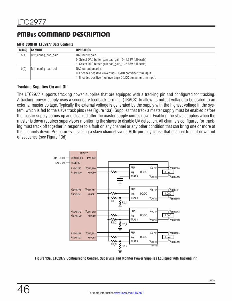
LTC2977
462977fc
For more information www.linear.com/LTC2977
MFR_CONFIG_LTC2977 Data ContentsBIT(S) SYMBOL OPERATION
b[1] Mfr_config_dac_gain DAC buffer gain.0: Select DAC buffer gain dac_gain_0 (1.38V full-scale)1: Select DAC buffer gain dac_gain_1 (2.65V full-scale)
b[0] Mfr_config_dac_pol DAC output polarity.0: Encodes negative (inverting) DC/DC converter trim input. 1: Encodes positive (noninverting) DC/DC converter trim input.
Tracking Supplies On and Off
The LTC2977 supports tracking power supplies that are equipped with a tracking pin and configured for tracking. A tracking power supply uses a secondary feedback terminal (TRACK) to allow its output voltage to be scaled to an external master voltage. Typically the external voltage is generated by the supply with the highest voltage in the sys-tem, which is fed to the slave track pins (see Figure 13a). Supplies that track a master supply must be enabled before the master supply comes up and disabled after the master supply comes down. Enabling the slave supplies when the master is down requires supervisors monitoring the slaves to disable UV detection. All channels configured for track-ing must track off together in response to a fault on any channel or any other condition that can bring one or more of the channels down. Prematurely disabling a slave channel via its RUN pin may cause that channel to shut down out of sequence (see Figure 13d)
PMBus COMMAND DESCRIPTION
Figure 13a. LTC2977 Configured to Control, Supervise and Monitor Power Supplies Equipped with Tracking Pin
VOUTPRUN
VOUTM
VSENSEP0
VSENSEM0TRACK
FAULT00FAULTB0
LTC2977
CONTROL0
VOUT_EN0
CONTROL0
DC/DC LOAD
VOUTPRUN
VOUTM
VSENSEP1
VSENSEM1TRACK
VOUT_EN1
DC/DC LOAD
VOUTPRUN
VOUTM
VSENSEP2
VSENSEM2TRACK
VOUT_EN2
DC/DC LOAD
VOUTPRUN
VOUTM
VSENSEP3
VSENSEM3TRACK
VFBVDACP0
VFBVDACP1
VDACP3
VFBVDACP2
VFB
VOUT_EN3
VSENSEP0
VSENSEP1
VSENSEP2
VSENSEM0
VSENSEM1
VSENSEM3
VSENSEM2
VSENSEP3
DC/DC LOAD
2977 F13aR2_3R1_3
R2_2R1_2
R2_1R1_1
PWRGD
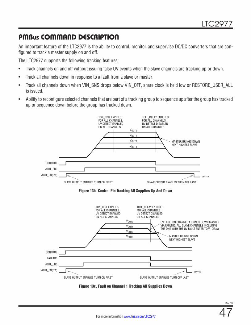
LTC2977
472977fc
For more information www.linear.com/LTC2977
An important feature of the LTC2977 is the ability to control, monitor, and supervise DC/DC converters that are con-figured to track a master supply on and off.
The LTC2977 supports the following tracking features:
• Track channels on and off without issuing false UV events when the slave channels are tracking up or down.
• Track all channels down in response to a fault from a slave or master.
• Track all channels down when VIN_SNS drops below VIN_OFF, share clock is held low or RESTORE_USER_ALL is issued.
• Ability to reconfigure selected channels that are part of a tracking group to sequence up after the group has tracked up or sequence down before the group has tracked down.
PMBus COMMAND DESCRIPTION
Figure 13b. Control Pin Tracking All Supplies Up And Down
Figure 13c. Fault on Channel 1 Tracking All Supplies Down
VOUT2
VOUT3
VOUT_EN(3:1)2977 F13b
VOUT_EN0
CONTROL
SLAVE OUTPUT ENABLES TURN ON FIRST SLAVE OUTPUT ENABLES TURN OFF LAST
MASTER BRINGS DOWNNEXT HIGHEST SLAVE
TON_RISE EXPIRES FOR ALL CHANNELS. UV DETECT ENABLED ON ALL CHANNELS
TOFF_DELAY ENTERED FOR ALL CHANNELS.UV DETECT DISABLED ON ALL CHANNELS
VOUT1
VOUT0
VOUT2
VOUT3
VOUT_EN(3:1)2977 F13c
VOUT_EN0
FAULTB0
CONTROL
UV FAULT ON CHANNEL 1 BRINGS DOWN MASTERVIA FAULTB0. ALL SLAVE CHANNELS INCLUDINGTHE ONE WITH THE UV FAULT ENTER TOFF_DELAY
SLAVE OUTPUT ENABLES TURN ON FIRST SLAVE OUTPUT ENABLES TURN OFF LAST
MASTER BRINGS DOWNNEXT HIGHEST SLAVE
TON_RISE EXPIRES FOR ALL CHANNELS. UV DETECT ENABLED ON ALL CHANNELS
TOFF_DELAY ENTERED FOR ALL CHANNELS.UV DETECT DISABLED ON ALL CHANNELS
VOUT1
VOUT0
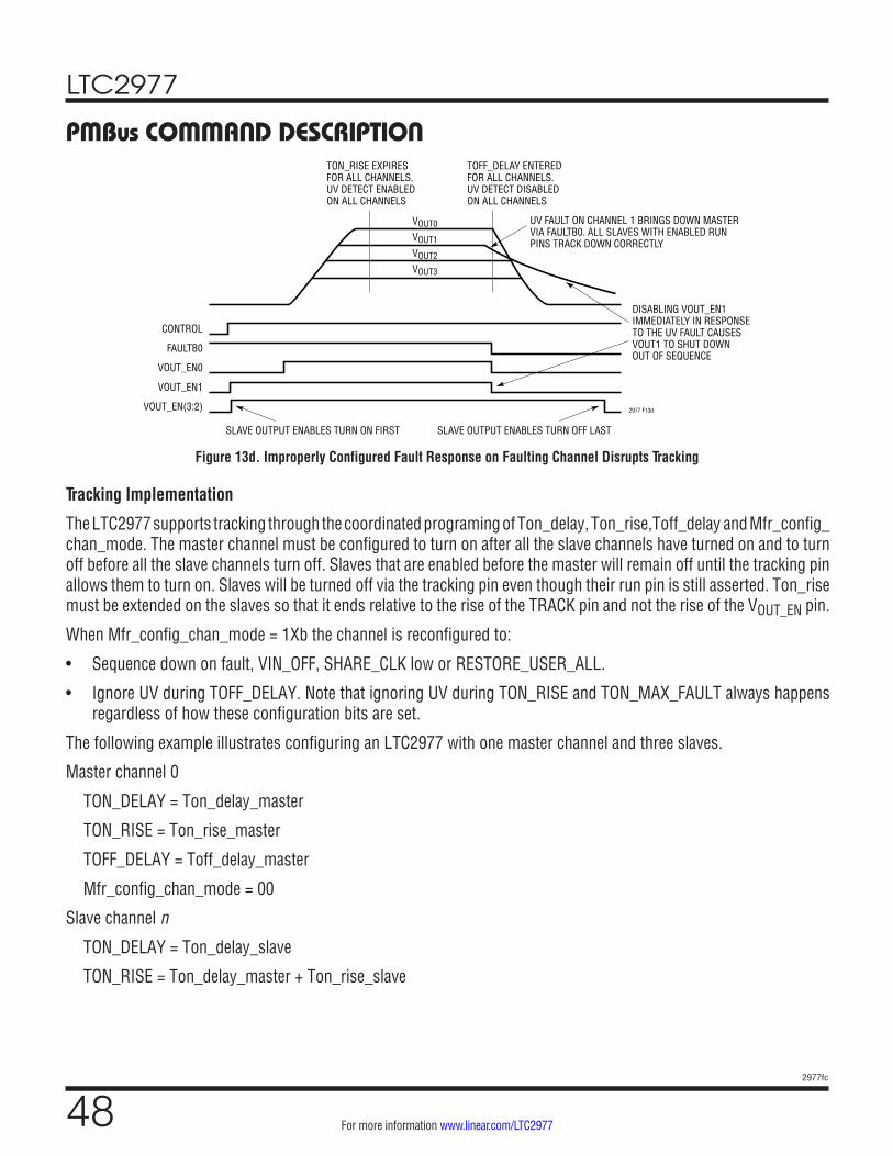
LTC2977
482977fc
For more information www.linear.com/LTC2977
Tracking Implementation
The LTC2977 supports tracking through the coordinated programing of Ton_delay, Ton_rise,Toff_delay and Mfr_config_chan_mode. The master channel must be configured to turn on after all the slave channels have turned on and to turn off before all the slave channels turn off. Slaves that are enabled before the master will remain off until the tracking pin allows them to turn on. Slaves will be turned off via the tracking pin even though their run pin is still asserted. Ton_rise must be extended on the slaves so that it ends relative to the rise of the TRACK pin and not the rise of the VOUT_EN pin.
When Mfr_config_chan_mode = 1Xb the channel is reconfigured to:
• Sequence down on fault, VIN_OFF, SHARE_CLK low or RESTORE_USER_ALL.
• Ignore UV during TOFF_DELAY. Note that ignoring UV during TON_RISE and TON_MAX_FAULT always happens regardless of how these configuration bits are set.
The following example illustrates configuring an LTC2977 with one master channel and three slaves.
Master channel 0
TON_DELAY = Ton_delay_master
TON_RISE = Ton_rise_master
TOFF_DELAY = Toff_delay_master
Mfr_config_chan_mode = 00
Slave channel n
TON_DELAY = Ton_delay_slave
TON_RISE = Ton_delay_master + Ton_rise_slave
PMBus COMMAND DESCRIPTION
Figure 13d. Improperly Configured Fault Response on Faulting Channel Disrupts Tracking
VOUT2
VOUT3
VOUT_EN(3:2) 2977 F13d
VOUT_EN1
VOUT_EN0
FAULTB0
CONTROL
UV FAULT ON CHANNEL 1 BRINGS DOWN MASTERVIA FAULTB0. ALL SLAVES WITH ENABLED RUNPINS TRACK DOWN CORRECTLY
SLAVE OUTPUT ENABLES TURN ON FIRST SLAVE OUTPUT ENABLES TURN OFF LAST
DISABLING VOUT_EN1 IMMEDIATELY IN RESPONSE TO THE UV FAULT CAUSES VOUT1 TO SHUT DOWN OUT OF SEQUENCE
TON_RISE EXPIRES FOR ALL CHANNELS. UV DETECT ENABLED ON ALL CHANNELS
TOFF_DELAY ENTERED FOR ALL CHANNELS.UV DETECT DISABLED ON ALL CHANNELS
VOUT1
VOUT0
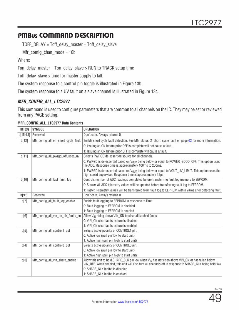
LTC2977
492977fc
For more information www.linear.com/LTC2977
TOFF_DELAY = Toff_delay_master + Toff_delay_slave
Mfr_config_chan_mode = 10b
Where:
Ton_delay_master – Ton_delay_slave > RUN to TRACK setup time
Toff_delay_slave > time for master supply to fall.
The system response to a control pin toggle is illustrated in Figure 13b.
The system response to a UV fault on a slave channel is illustrated in Figure 13c.
MFR_CONFIG_ALL_LTC2977
This command is used to configure parameters that are common to all channels on the IC. They may be set or reviewed from any PAGE setting.
MFR_CONFIG_ALL_LTC2977 Data Contents
BIT(S) SYMBOL OPERATIONb[15-13] Reserved Don’t care. Always returns 0
b[12] Mfr_config_all_en_short_cycle_fault Enable short cycle fault detection. See Mfr_status_2_short_cycle_fault on page 62 for more information.0: Issuing an ON before prior OFF is complete will not cause a fault.1: Issuing an ON before prior OFF is complete will cause a fault.
b[11] Mfr_config_all_pwrgd_off_uses_uv Selects PWRGD de-assertion source for all channels.0: PWRGD is de-asserted based on VOUT being below or equal to POWER_GOOD_OFF. This option uses the ADC. Response time is approximately 100ms to 200ms.1: PWRGD is de-asserted based on VOUT being below or equal to VOUT_UV_LIMIT. This option uses the high speed supervisor. Response time is approximately 12µs
b[10] Mfr_config_all_fast_fault_log Controls number of ADC readings completed before transferring fault log memory to EEPROM.0: Slower. All ADC telemetry values will be updated before transferring fault log to EEPROM.1: Faster. Telemetry values will be transferred from fault log to EEPROM within 24ms after detecting fault.
b[9:8] Reserved Don’t care. Always returns 0
b[7] Mfr_config_all_fault_log_enable Enable fault logging to EEPROM in response to Fault.0: Fault logging to EEPROM is disabled1: Fault logging to EEPROM is enabled
b[6] Mfr_config_all_vin_on_clr_faults_en Allow VIN rising above VIN_ON to clear all latched faults0: VIN_ON clear faults feature is disabled1: VIN_ON clear faults feature is enabled
b[5] Mfr_config_all_control1_pol Selects active polarity of CONTROL1 pin.0: Active low (pull pin low to start unit)1: Active high (pull pin high to start unit)
b[4] Mfr_config_all_control0_pol Selects active polarity of CONTROL0 pin.0: Active low (pull pin low to start unit)1: Active high (pull pin high to start unit)
b[3] Mfr_config_all_vin_share_enable Allow this unit to hold SHARE_CLK pin low when VIN has not risen above VIN_ON or has fallen below VIN_OFF. When enabled, this unit will also turn all channels off in response to SHARE_CLK being held low.0: SHARE_CLK inhibit is disabled1: SHARE_CLK inhibit is enabled
PMBus COMMAND DESCRIPTION
LTC2977
502977fc
For more information www.linear.com/LTC2977
MFR_CONFIG_ALL_LTC2977 Data Contents
BIT(S) SYMBOL OPERATIONb[2] Mfr_config_all_pec_en PMBus packet error checking enable.
0: PEC is accepted but not required1: PEC is required
b[1] Mfr_config_all_longer_pmbus_timeout
Increase PMBus timeout internal by a factor of 8. Recommended for fault logging.0: PMBus timeout is not multiplied by a factor of 81: PMBus timeout is multiplied by a factor of 8
b[0] Mfr_config_all_vinen_wpu_dis VIN_EN charge-pumped, current-limited pull-up disable. 0: Use weak current-limited pull-up on VIN_EN after power-up, as long as no faults have forced VIN_EN off.1: Disable weak pull-up. VIN_EN driver is three-stated after power-up as long as no faults have forced VIN_EN off.
MFR_FAULTBz0_PROPAGATE, MFR_FAULTBz1_PROPAGATE
These manufacturer specific commands enable channels that have faulted off to propagate that state to the appropri-ate fault pin. Faulted off states for pages 0 through 3 can only be propagated to pins FAULTB00 and FAULTB01; this is referred to as zone 0. Faulted off states for pages 4 through 7 can only be propagated to pins FAULTB10 and FAULTB11; this is referred to as zone 1. The z designator in the command name is used to indicate that this command affects different zones depending on the page. See Figure 20.
Note that pulling a fault pin low will have no effect for channels that have MFR_FAULTBzn_RESPONSE set to 0. The channel continues operation without interruption. This fault response is called Ignore (0x0) in LTpowerPlay.
MFR_FAULTBz0_PROPAGATE Data ContentBIT(S) SYMBOL OPERATION
b[7:1] Reserved Don’t care. Always returns 0.
b[0] Mfr_faultbz0_propagate Enable fault propagation.For pages 0 through 3, zone 0 0: Channel’s faulted off state does not assert FAULTB00 low. 1: Channel’s faulted off state asserts FAULTB00 low.For pages 4 through 7, zone 1 0: Channel’s faulted off state does not assert FAULTB10 low. 1: Channel’s faulted off state asserts FAULTB10 low.
MFR_FAULTBz1_PROPAGATE Data ContentBIT(S) SYMBOL OPERATION
b[7:1] Reserved Don’t care. Always returns 0.
b[0] Mfr_faultbz1_propagate Enable fault propagation.For pages 0 through 3, zone 0 0: Channel’s faulted off state does not assert FAULTB01 low. 1: Channel’s faulted off state asserts FAULTB01 low.For pages 4 through 7, zone 1 0: Channel’s faulted off state does not assert FAULTB11 low. 1: Channel’s faulted off state asserts FAULTB11 low.
PMBus COMMAND DESCRIPTION
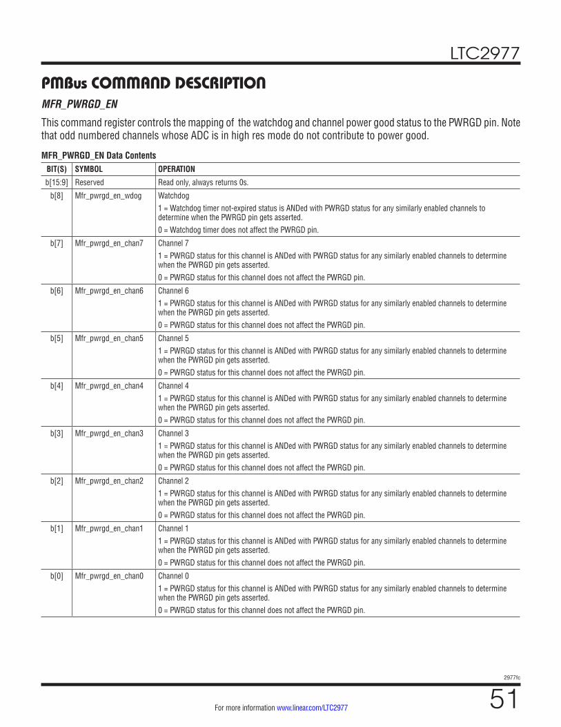
LTC2977
512977fc
For more information www.linear.com/LTC2977
MFR_PWRGD_EN
This command register controls the mapping of the watchdog and channel power good status to the PWRGD pin. Note that odd numbered channels whose ADC is in high res mode do not contribute to power good.
MFR_PWRGD_EN Data ContentsBIT(S) SYMBOL OPERATION
b[15:9] Reserved Read only, always returns 0s.
b[8] Mfr_pwrgd_en_wdog Watchdog1 = Watchdog timer not-expired status is ANDed with PWRGD status for any similarly enabled channels to determine when the PWRGD pin gets asserted.0 = Watchdog timer does not affect the PWRGD pin.
b[7] Mfr_pwrgd_en_chan7 Channel 7 1 = PWRGD status for this channel is ANDed with PWRGD status for any similarly enabled channels to determine when the PWRGD pin gets asserted.0 = PWRGD status for this channel does not affect the PWRGD pin.
b[6] Mfr_pwrgd_en_chan6 Channel 6 1 = PWRGD status for this channel is ANDed with PWRGD status for any similarly enabled channels to determine when the PWRGD pin gets asserted.0 = PWRGD status for this channel does not affect the PWRGD pin.
b[5] Mfr_pwrgd_en_chan5 Channel 5 1 = PWRGD status for this channel is ANDed with PWRGD status for any similarly enabled channels to determine when the PWRGD pin gets asserted.0 = PWRGD status for this channel does not affect the PWRGD pin.
b[4] Mfr_pwrgd_en_chan4 Channel 4 1 = PWRGD status for this channel is ANDed with PWRGD status for any similarly enabled channels to determine when the PWRGD pin gets asserted.0 = PWRGD status for this channel does not affect the PWRGD pin.
b[3] Mfr_pwrgd_en_chan3 Channel 3 1 = PWRGD status for this channel is ANDed with PWRGD status for any similarly enabled channels to determine when the PWRGD pin gets asserted.0 = PWRGD status for this channel does not affect the PWRGD pin.
b[2] Mfr_pwrgd_en_chan2 Channel 2 1 = PWRGD status for this channel is ANDed with PWRGD status for any similarly enabled channels to determine when the PWRGD pin gets asserted.0 = PWRGD status for this channel does not affect the PWRGD pin.
b[1] Mfr_pwrgd_en_chan1 Channel 1 1 = PWRGD status for this channel is ANDed with PWRGD status for any similarly enabled channels to determine when the PWRGD pin gets asserted.0 = PWRGD status for this channel does not affect the PWRGD pin.
b[0] Mfr_pwrgd_en_chan0 Channel 0 1 = PWRGD status for this channel is ANDed with PWRGD status for any similarly enabled channels to determine when the PWRGD pin gets asserted.0 = PWRGD status for this channel does not affect the PWRGD pin.
PMBus COMMAND DESCRIPTION
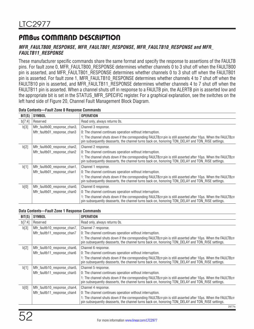
LTC2977
522977fc
For more information www.linear.com/LTC2977
MFR_FAULTB00_RESPONSE, MFR_FAULTB01_RESPONSE, MFR_FAULTB10_RESPONSE and MFR_FAULTB11_RESPONSE
These manufacturer specific commands share the same format and specify the response to assertions of the FAULTB pins. For fault zone 0, MFR_FAULTB00_RESPONSE determines whether channels 0 to 3 shut off when the FAULTB00 pin is asserted, and MFR_FAULTB01_RESPONSE determines whether channels 0 to 3 shut off when the FAULTB01 pin is asserted. For fault zone 1, MFR_FAULTB10_RESPONSE determines whether channels 4 to 7 shut off when the FAULTB10 pin is asserted, and MFR_FAULTB11_RESPONSE determines whether channels 4 to 7 shut off when the FAULTB11 pin is asserted. When a channel shuts off in response to a FAULTB pin, the ALERTB pin is asserted low and the appropriate bit is set in the STATUS_MFR_SPECIFIC register. For a graphical explanation, see the switches on the left hand side of Figure 20, Channel Fault Management Block Diagram.
Data Contents—Fault Zone 0 Response CommandsBIT(S) SYMBOL OPERATIONb[7:4] Reserved Read only, always returns 0s.b[3] Mfr_faultb00_response_chan3,
Mfr_faultb01_response_chan3Channel 3 response.0: The channel continues operation without interruption.1: The channel shuts down if the corresponding FAULTBzn pin is still asserted after 10µs. When the FAULTBzn pin subsequently deasserts, the channel turns back on, honoring TON_DELAY and TON_RISE settings.
b[2] Mfr_faultb00_response_chan2,Mfr_faultb01_response_chan2
Channel 2 response.0: The channel continues operation without interruption.1: The channel shuts down if the corresponding FAULTBzn pin is still asserted after 10µs. When the FAULTBzn pin subsequently deasserts, the channel turns back on, honoring TON_DELAY and TON_RISE settings.
b[1] Mfr_faultb00_response_chan1,Mfr_faultb01_response_chan1
Channel 1 response.0: The channel continues operation without interruption.1: The channel shuts down if the corresponding FAULTBzn pin is still asserted after 10µs. When the FAULTBzn pin subsequently deasserts, the channel turns back on, honoring TON_DELAY and TON_RISE settings.
b[0] Mfr_faultb00_response_chan0,Mfr_faultb01_response_chan0
Channel 0 response.0: The channel continues operation without interruption.1: The channel shuts down if the corresponding FAULTBzn pin is still asserted after 10µs. When the FAULTBzn pin subsequently deasserts, the channel turns back on, honoring TON_DELAY and TON_RISE settings.
Data Contents—Fault Zone 1 Response CommandsBIT(S) SYMBOL OPERATIONb[7:4] Reserved Read only, always returns 0s.b[3] Mfr_faultb10_response_chan7,
Mfr_faultb11_response_chan7Channel 7 response.0: The channel continues operation without interruption.1: The channel shuts down if the corresponding FAULTBzn pin is still asserted after 10µs. When the FAULTBzn pin subsequently deasserts, the channel turns back on, honoring TON_DELAY and TON_RISE settings.
b[2] Mfr_faultb10_response_chan6,Mfr_faultb11_response_chan6
Channel 6 response.0: The channel continues operation without interruption.1: The channel shuts down if the corresponding FAULTBzn pin is still asserted after 10µs. When the FAULTBzn pin subsequently deasserts, the channel turns back on, honoring TON_DELAY and TON_RISE settings.
b[1] Mfr_faultb10_response_chan5,Mfr_faultb11_response_chan5
Channel 5 response.0: The channel continues operation without interruption.1: The channel shuts down if the corresponding FAULTBzn pin is still asserted after 10µs. When the FAULTBzn pin subsequently deasserts, the channel turns back on, honoring TON_DELAY and TON_RISE settings.
b[0] Mfr_faultb10_response_chan4,Mfr_faultb11_response_chan4
Channel 4 response.0: The channel continues operation without interruption.1: The channel shuts down if the corresponding FAULTBzn pin is still asserted after 10µs. When the FAULTBzn pin subsequently deasserts, the channel turns back on, honoring TON_DELAY and TON_RISE settings.
PMBus COMMAND DESCRIPTION
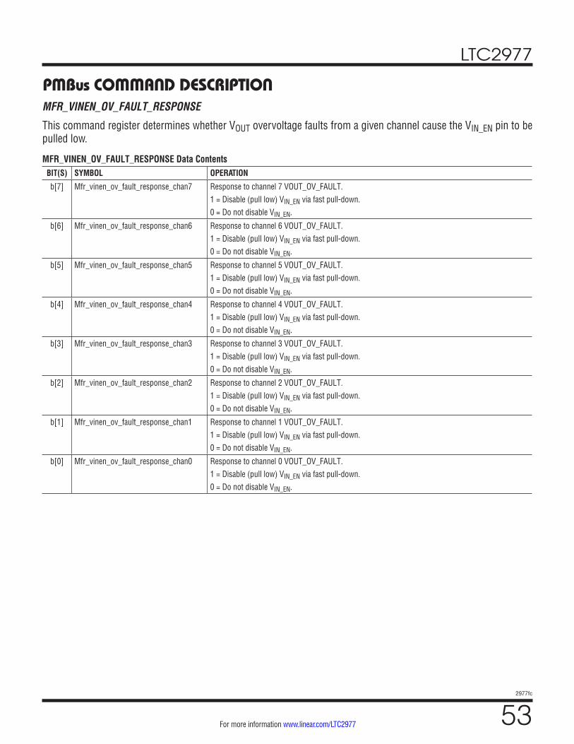
LTC2977
532977fc
For more information www.linear.com/LTC2977
MFR_VINEN_OV_FAULT_RESPONSE
This command register determines whether VOUT overvoltage faults from a given channel cause the VIN_EN pin to be pulled low.
MFR_VINEN_OV_FAULT_RESPONSE Data ContentsBIT(S) SYMBOL OPERATION
b[7] Mfr_vinen_ov_fault_response_chan7 Response to channel 7 VOUT_OV_FAULT.1 = Disable (pull low) VIN_EN via fast pull-down.0 = Do not disable VIN_EN.
b[6] Mfr_vinen_ov_fault_response_chan6 Response to channel 6 VOUT_OV_FAULT.1 = Disable (pull low) VIN_EN via fast pull-down.0 = Do not disable VIN_EN.
b[5] Mfr_vinen_ov_fault_response_chan5 Response to channel 5 VOUT_OV_FAULT.1 = Disable (pull low) VIN_EN via fast pull-down.0 = Do not disable VIN_EN.
b[4] Mfr_vinen_ov_fault_response_chan4 Response to channel 4 VOUT_OV_FAULT.1 = Disable (pull low) VIN_EN via fast pull-down.0 = Do not disable VIN_EN.
b[3] Mfr_vinen_ov_fault_response_chan3 Response to channel 3 VOUT_OV_FAULT.1 = Disable (pull low) VIN_EN via fast pull-down.0 = Do not disable VIN_EN.
b[2] Mfr_vinen_ov_fault_response_chan2 Response to channel 2 VOUT_OV_FAULT.1 = Disable (pull low) VIN_EN via fast pull-down.0 = Do not disable VIN_EN.
b[1] Mfr_vinen_ov_fault_response_chan1 Response to channel 1 VOUT_OV_FAULT.1 = Disable (pull low) VIN_EN via fast pull-down.0 = Do not disable VIN_EN.
b[0] Mfr_vinen_ov_fault_response_chan0 Response to channel 0 VOUT_OV_FAULT.1 = Disable (pull low) VIN_EN via fast pull-down.0 = Do not disable VIN_EN.
PMBus COMMAND DESCRIPTION
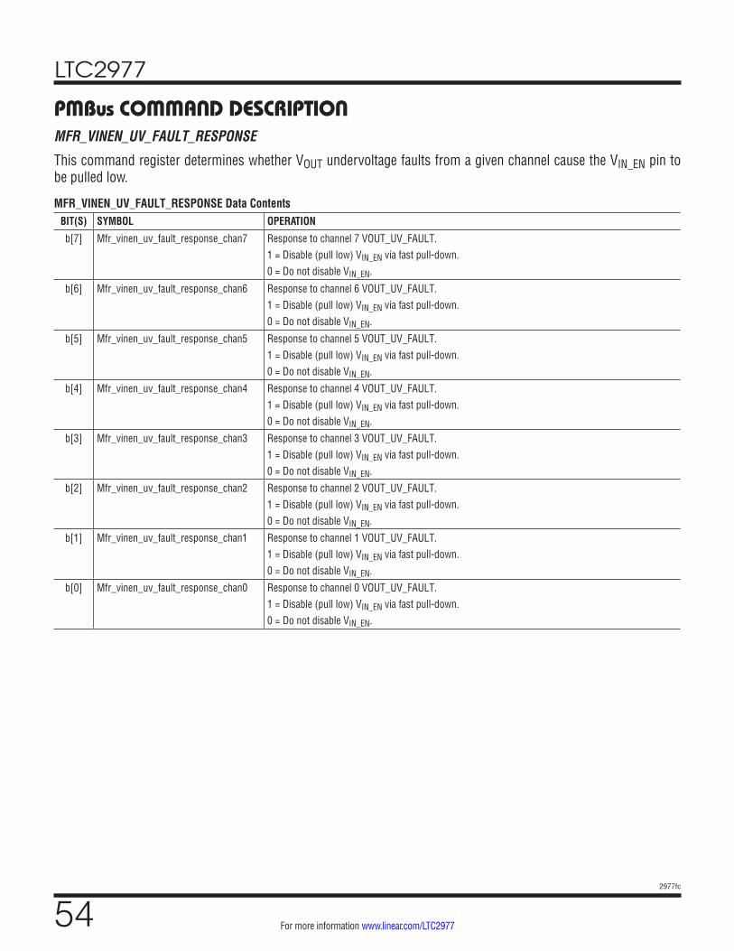
LTC2977
542977fc
For more information www.linear.com/LTC2977
MFR_VINEN_UV_FAULT_RESPONSE
This command register determines whether VOUT undervoltage faults from a given channel cause the VIN_EN pin to be pulled low.
MFR_VINEN_UV_FAULT_RESPONSE Data ContentsBIT(S) SYMBOL OPERATION
b[7] Mfr_vinen_uv_fault_response_chan7 Response to channel 7 VOUT_UV_FAULT.1 = Disable (pull low) VIN_EN via fast pull-down.0 = Do not disable VIN_EN.
b[6] Mfr_vinen_uv_fault_response_chan6 Response to channel 6 VOUT_UV_FAULT.1 = Disable (pull low) VIN_EN via fast pull-down.0 = Do not disable VIN_EN.
b[5] Mfr_vinen_uv_fault_response_chan5 Response to channel 5 VOUT_UV_FAULT.1 = Disable (pull low) VIN_EN via fast pull-down.0 = Do not disable VIN_EN.
b[4] Mfr_vinen_uv_fault_response_chan4 Response to channel 4 VOUT_UV_FAULT.1 = Disable (pull low) VIN_EN via fast pull-down.0 = Do not disable VIN_EN.
b[3] Mfr_vinen_uv_fault_response_chan3 Response to channel 3 VOUT_UV_FAULT.1 = Disable (pull low) VIN_EN via fast pull-down.0 = Do not disable VIN_EN.
b[2] Mfr_vinen_uv_fault_response_chan2 Response to channel 2 VOUT_UV_FAULT.1 = Disable (pull low) VIN_EN via fast pull-down.0 = Do not disable VIN_EN.
b[1] Mfr_vinen_uv_fault_response_chan1 Response to channel 1 VOUT_UV_FAULT.1 = Disable (pull low) VIN_EN via fast pull-down.0 = Do not disable VIN_EN.
b[0] Mfr_vinen_uv_fault_response_chan0 Response to channel 0 VOUT_UV_FAULT.1 = Disable (pull low) VIN_EN via fast pull-down.0 = Do not disable VIN_EN.
PMBus COMMAND DESCRIPTION
LTC2977
552977fc
For more information www.linear.com/LTC2977
PMBus COMMAND DESCRIPTIONMFR_RETRY_COUNT
The MFR_RETRY_COUNT is a global command that sets the number of retries attempted when any channel faults off with its fault response retry field set to a non zero value.
In the event of multiple or recurring retry faults on the same channel the total number of retries equals MFR_RETRY_COUNT. If a channel has not been faulted off for 6 seconds, its retry counter is cleared. Toggling a channel’s CONTROL pin off then on or issuing OPERATION off then on commands will synchronously clear the retry count. Writing to MFR_RETRY_COUNT clears the retry count for all channels
MFR_RETRY_COUNT Data ContentsBIT(S) SYMBOL OPERATION
b[7:3] Reserved Always returns zero.
b[2:0] Mfr_retry_count [2:0] 0: No retries:1-6: Number of retries.7: Infinite retries.
MFR_RETRY_DELAY
This command determines the retry interval when the LTC2977 is in retry mode in response to a fault condition. The read value of this command always returns what was last written and does not reflect internal limiting.
MFR_RETRY_DELAY Data ContentsBIT(S) SYMBOL OPERATION
b[15:0] Mfr_retry_delay The data uses the L11 format.This delay is counted using SHARE_CLK only.Delays are rounded to the nearest 200µs.Units: ms. Max delay is 13.1 sec.
MFR_RESTART_DELAY
This command sets the minimum off time of a CONTROL initiated restart. If the CONTROL pin is toggled off for at least 10µs then on, all dependent channels are disabled, held off for a time = Mfr_restart_delay, then sequenced back on. CONTROLn pin transitions whose OFF time exceeds Mfr_restart_delay are not affected by this command. A value of all zeros disables this feature. The read value of this command always returns what was last written and does not reflect internal limiting.
MFR_RESTART_DELAY Data ContentsBIT(S) SYMBOL OPERATION
b[15:0] Mfr_restart_delay The data uses the L11 format.This delay is counted using SHARE_CLK only.Delays are rounded to the nearest 200µs.Units: ms. Max delay is 13.1 sec.
LTC2977
562977fc
For more information www.linear.com/LTC2977
PMBus COMMAND DESCRIPTIONMFR_VOUT_PEAK
This command returns the maximum ADC measured value of the channel’s output voltage. This command is not supported for odd channels that are configured to measure current. This register is reset to 0xF800 (0.0) when the LTC2977 emerges from power-on reset, or when a CLEAR_FAULTS command to the page is executed, or the channel goes through an off-to-on transition.
MFR_VOUT_PEAK Data ContentsBIT(S) SYMBOL OPERATION
b[15:0] Mfr_vout_peak[15:0] The data uses the L16 format.Units: V.
MFR_VIN_PEAK
This command returns the maximum ADC measured value of the input voltage. This register is reset to 0x7C00 (–225) when the LTC2977 emerges from power-on reset, or when a CLEAR_FAULTS command to any page is executed, or a channel goes through an off-to-on transition.
MFR_VIN_PEAK Data ContentsBIT(S) SYMBOL OPERATION
b[15:0] Mfr_vin_peak[15:0] The data uses the L11 format.Units: V
MFR_TEMPERATURE_PEAK
This command returns the maximum ADC measured value of junction temperature in °C as determined by the LTC2977’s internal temperature sensor. This register is reset to 0x7C00 (–225) when the LTC2977 emerges from power-on reset, when a CLEAR_FAULTS command to any page is executed, or a channel goes through an off-to-on transition.
MFR_TEMPERATURE_PEAK Data ContentsBIT(S) SYMBOL OPERATION
b[15:0] Mfr_temperature_peak[15:0] The data uses the L11 format.Units: °C.
MFR_DAC
This command register allows the user to directly program the 10-bit DAC. Manual DAC writes require the channel to be in the ON state,TON_RISE to have expired and MFR_CONFIG_LTC2977 b[5:4] = 10b or 11b. Writing MFR_CONFIG_LTC2977 b[5:4] = 10b commands the DAC to hard-connect with the value in Mfr_dac_direct_val. Writing b[5:4] = 11b commands the DAC to soft-connect. Once the DAC has soft-connected, Mfr_dac_direct_val returns the value that allowed the DAC to be connected without perturbing the power supply. MFR_DAC writes are ignored when MFR_CONFIG_LTC2977 b[5:4] = 00b or 01b.
MFR_DAC Data ContentsBIT(S) SYMBOL OPERATION
b[15:10] Reserved Read only, always returns 0.
b[9:0] Mfr_dac_direct_val DAC code value.
LTC2977
572977fc
For more information www.linear.com/LTC2977
PMBus COMMAND DESCRIPTIONMFR_POWERGOOD_ASSERTION_DELAY
This command register allows the user to program the delay from when the internal power good signal becomes valid until the power good output is asserted. This delay is counted using SHARE_CLK if available, otherwise the internal oscillator is used. This delay is internally limited to 13.1 seconds, and rounded to the nearest 200µs. The read value of this command always returns what was last written and does not reflect internal limiting.
The power good de-assertion delay and threshold source is controlled by Mfr_config_all_pwrgd_off_uses_uv. Sys-tems that require a fast power good de-assertion should set Mfr_config_all_pwrgd_off_uses_uv=1. This uses the VOUT_UV_FAULT_LIMIT and the high speed comparator to de-assert the PWRGD pin. Systems that require a separate power good off threshold should set Mfr_config_all_pwrgd_off_uses_uv=0. This uses the slower ADC polling loop and POWER_GOOD_OFF to de-assert the PWRGD pin.
MFR_POWERGOOD_ASSERTION_DELAY Data ContentsBIT(S) SYMBOL OPERATION
b[15:0] Mfr_powergood_assertion_delay The data uses the L11 format.This delay is counted using SHARE_CLK if available, otherwise the internal oscillator is used.Delays are rounded to the nearest 200µs.Units: ms. Max delay is 13.1 sec.
MFR_PADS
The MFR_PADS command provides read only access to slow frequency digital pads (pins). The input values presented in bits[9:0] are before any deglitching logic.
MFR_PADS Data ContentsBIT(S) SYMBOL OPERATIONb[15] Mfr_pads_pwrgd_drive 0 = PWRGD pad is being driven low by this chip
1 = PWRGD pad is not being driven low by this chipb[14] Mfr_pads_alertb_drive 0 = ALERTB pad is being driven low by this chip
1 = ALERTB pad is not being driven low by this chipb[13:10] Mfr_pads_faultb_drive[3:0] Bit[3] used for FAULTB00 pad, bit[2] used for FAULTB01 pad, bit[1] used for FAULTB10 pad, bit[0] used for
FAULTB11 pad as follows:0 = FAULTBzn pad is being driven low by this chip1 = FAULTBzn pad is not being driven low by this chip
b[9:8] Mfr_pads_asel1[1:0] 11: Logic high detected on ASEL1 input pad10: ASEL1 input pad is floating01: Reserved00: Logic low detected on ASEL1 input pad
b[7:6] Mfr_pads_asel0[1:0] 11: Logic high detected on ASEL0 input pad10: ASEL0 input pad is floating01: Reserved00: Logic low detected on ASEL0 input pad
b[5] Mfr_pads_control1 1: Logic high detected on CONTROL1 pad0: Logic low detected on CONTROL1 pad
b[4] Mfr_pads_control0 1: Logic high detected on CONTROL0 pad0: Logic low detected on CONTROL0 pad
LTC2977
582977fc
For more information www.linear.com/LTC2977
PMBus COMMAND DESCRIPTIONMFR_PADS Data Contents
BIT(S) SYMBOL OPERATIONb[3:0] Mfr_pads_faultb[3:0] Bit[3] used for FAULTB00 pad, bit[2] used for FAULTB01 pad, bit[1] used for FAULTB10 pad, bit[0] used for
FAULTB11 pad as follows:1: Logic high detected on FAULTBzn pad0: Logic low detected on FAULTBzn pad
MFR_SPECIAL_ID
This register contains the manufacturer ID for the LTC2977.
MFR_SPECIAL_ID Data ContentsBIT(S) SYMBOL OPERATION
b[15:0] Mfr_special_id Read only, always returns 0x0131
MFR_SPECIAL_LOT
These paged registers contain information that identifies the user configuration that was programmed at the factory. Contact the factory to request a custom factory programmed user configuration and special lot number.
MFR_SPECIAL_LOT Data ContentsBIT(S) SYMBOL OPERATION
b[7:0] Mfr_special_lot Contains the LTC default special lot number. Contact the factory to request a custom factory programmed user configura-tion and special lot number.
MFR_INFO
The MFR_INFO register contains manufacturer specific information and is updated after a power-on reset, a RESTORE_USER_ALL command, or an EEPROM bulk read operation.
MFR_INFO Data ContentsBIT(S) SYMBOL OPERATION
b[15:6] Reserved Reserved
b[5] Mfr_info_ecc_user EEPROM ECC status.0: Corrections made in the EEPROM user space1: No corrections made in the EEPROM user space
b[4:0] Reserved Reserved
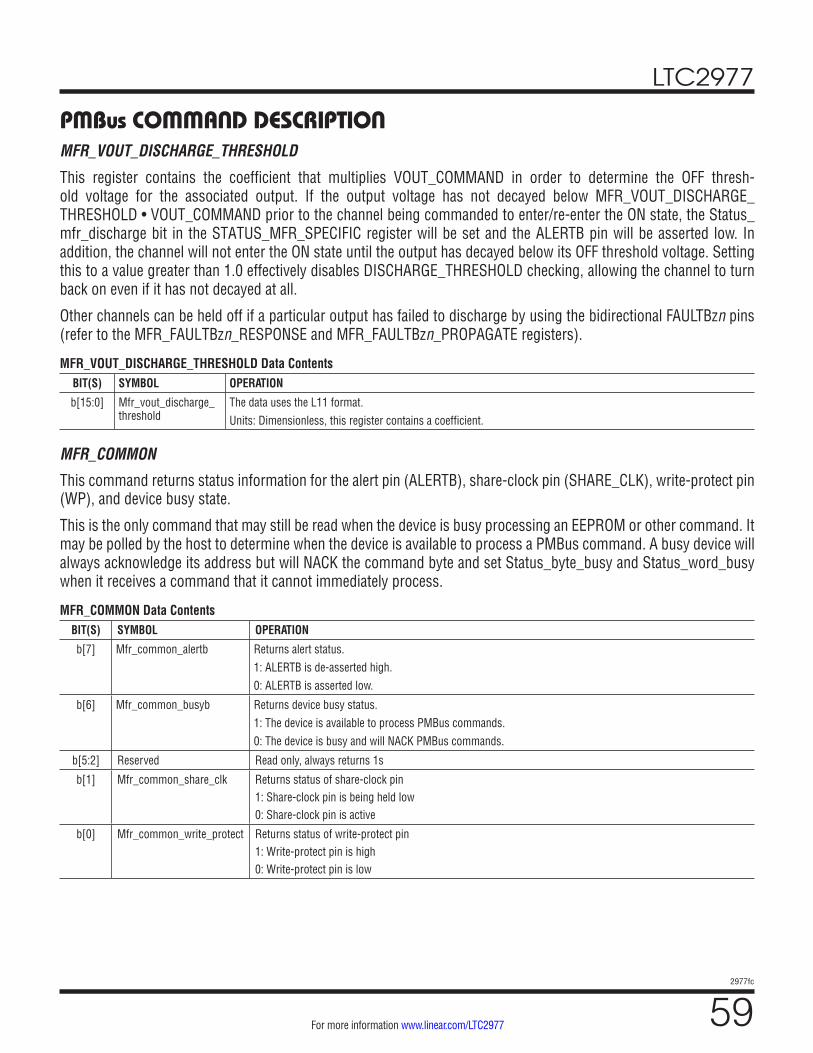
LTC2977
592977fc
For more information www.linear.com/LTC2977
PMBus COMMAND DESCRIPTIONMFR_VOUT_DISCHARGE_THRESHOLD
This register contains the coefficient that multiplies VOUT_COMMAND in order to determine the OFF thresh-old voltage for the associated output. If the output voltage has not decayed below MFR_VOUT_DISCHARGE_ THRESHOLD • VOUT_COMMAND prior to the channel being commanded to enter/re-enter the ON state, the Status_mfr_discharge bit in the STATUS_MFR_SPECIFIC register will be set and the ALERTB pin will be asserted low. In addition, the channel will not enter the ON state until the output has decayed below its OFF threshold voltage. Setting this to a value greater than 1.0 effectively disables DISCHARGE_THRESHOLD checking, allowing the channel to turn back on even if it has not decayed at all.
Other channels can be held off if a particular output has failed to discharge by using the bidirectional FAULTBzn pins (refer to the MFR_FAULTBzn_RESPONSE and MFR_FAULTBzn_PROPAGATE registers).
MFR_VOUT_DISCHARGE_THRESHOLD Data ContentsBIT(S) SYMBOL OPERATION
b[15:0] Mfr_vout_discharge_threshold
The data uses the L11 format.Units: Dimensionless, this register contains a coefficient.
MFR_COMMON
This command returns status information for the alert pin (ALERTB), share-clock pin (SHARE_CLK), write-protect pin (WP), and device busy state.
This is the only command that may still be read when the device is busy processing an EEPROM or other command. It may be polled by the host to determine when the device is available to process a PMBus command. A busy device will always acknowledge its address but will NACK the command byte and set Status_byte_busy and Status_word_busy when it receives a command that it cannot immediately process.
MFR_COMMON Data ContentsBIT(S) SYMBOL OPERATION
b[7] Mfr_common_alertb Returns alert status.1: ALERTB is de-asserted high.0: ALERTB is asserted low.
b[6] Mfr_common_busyb Returns device busy status.1: The device is available to process PMBus commands.0: The device is busy and will NACK PMBus commands.
b[5:2] Reserved Read only, always returns 1s
b[1] Mfr_common_share_clk Returns status of share-clock pin1: Share-clock pin is being held low0: Share-clock pin is active
b[0] Mfr_common_write_protect Returns status of write-protect pin1: Write-protect pin is high0: Write-protect pin is low
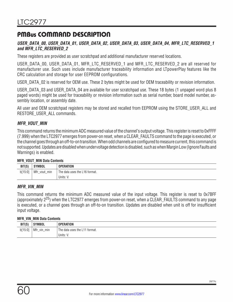
LTC2977
602977fc
For more information www.linear.com/LTC2977
PMBus COMMAND DESCRIPTIONUSER_DATA_00, USER_DATA_01, USER_DATA_02, USER_DATA_03, USER_DATA_04, MFR_LTC_RESERVED_1 and MFR_LTC_RESERVED_2
These registers are provided as user scratchpad and additional manufacturer reserved locations.
USER_DATA_00, USER_DATA_01, MFR_LTC_RESERVED_1 and MFR_LTC_RESERVED_2 are all reserved for manufacturer use. Such uses include manufacturer traceability information and LTpowerPlay features like the CRC calculation and storage for user EEPROM configurations.
USER_DATA_02 is reserved for OEM use. These 2 bytes might be used for OEM traceability or revision information.
USER_DATA_03 and USER_DATA_04 are available for user scratchpad use. These 18 bytes (1 unpaged word plus 8 paged words) might be used for traceability or revision information such as serial number, board model number, as-sembly location, or assembly date.
All user and OEM scratchpad registers may be stored and recalled from EEPROM using the STORE_USER_ALL and RESTORE_USER_ALL commands.
MFR_VOUT_MIN
This command returns the minimum ADC measured value of the channel’s output voltage. This register is reset to 0xFFFF (7.999) when the LTC2977 emerges from power-on reset, when a CLEAR_FAULTS command to the page is executed, or the channel goes through an off-to-on transition. When odd channels are configured to measure current, this command is not supported. Updates are disabled when undervoltage detection is disabled, such as when Margin Low (Ignore Faults and Warnings) is enabled.
MFR_VOUT_MIN Data ContentsBIT(S) SYMBOL OPERATION
b[15:0] Mfr_vout_min The data uses the L16 format.Units: V.
MFR_VIN_MIN
This command returns the minimum ADC measured value of the input voltage. This register is reset to 0x7BFF (approximately 225) when the LTC2977 emerges from power-on reset, when a CLEAR_FAULTS command to any page is executed, or a channel goes through an off-to-on transition. Updates are disabled when unit is off for insufficient input voltage.
MFR_VIN_MIN Data ContentsBIT(S) SYMBOL OPERATION
b[15:0] Mfr_vin_min The data uses the L11 format.Units: V.
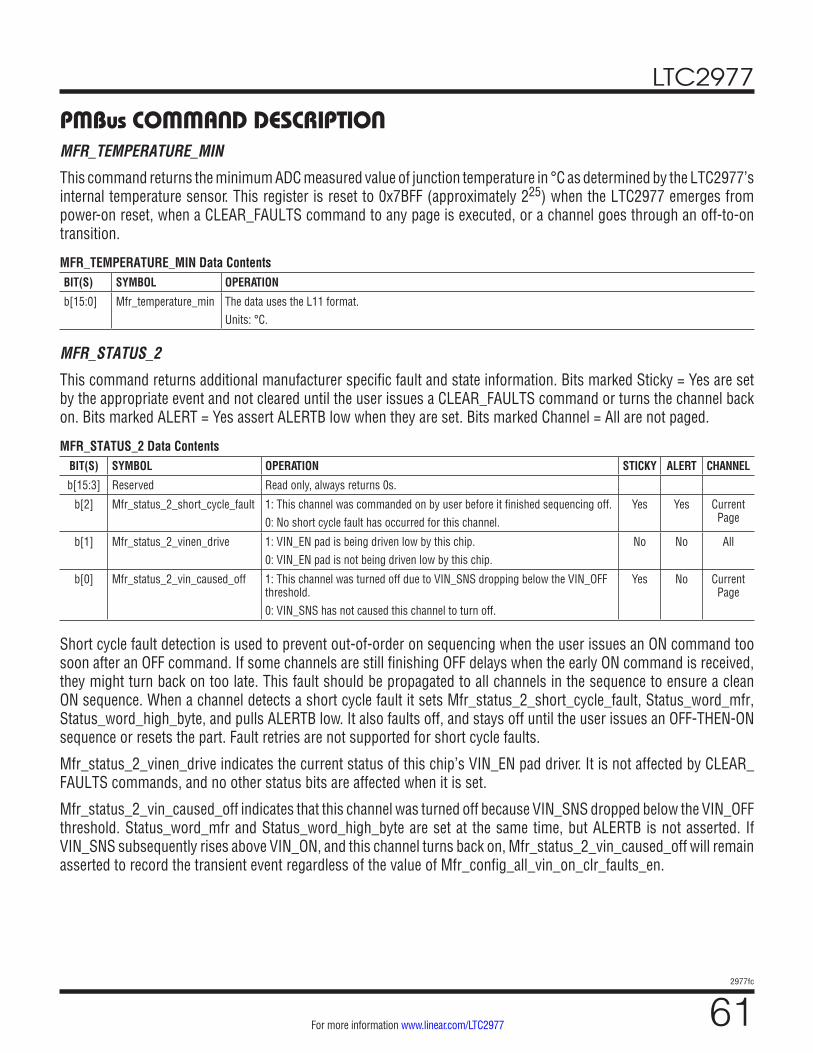
LTC2977
612977fc
For more information www.linear.com/LTC2977
PMBus COMMAND DESCRIPTIONMFR_TEMPERATURE_MIN
This command returns the minimum ADC measured value of junction temperature in °C as determined by the LTC2977’s internal temperature sensor. This register is reset to 0x7BFF (approximately 225) when the LTC2977 emerges from power-on reset, when a CLEAR_FAULTS command to any page is executed, or a channel goes through an off-to-on transition.
MFR_TEMPERATURE_MIN Data ContentsBIT(S) SYMBOL OPERATION
b[15:0] Mfr_temperature_min The data uses the L11 format.Units: °C.
MFR_STATUS_2
This command returns additional manufacturer specific fault and state information. Bits marked Sticky = Yes are set by the appropriate event and not cleared until the user issues a CLEAR_FAULTS command or turns the channel back on. Bits marked ALERT = Yes assert ALERTB low when they are set. Bits marked Channel = All are not paged.
MFR_STATUS_2 Data ContentsBIT(S) SYMBOL OPERATION STICKY ALERT CHANNEL
b[15:3] Reserved Read only, always returns 0s.
b[2] Mfr_status_2_short_cycle_fault 1: This channel was commanded on by user before it finished sequencing off.0: No short cycle fault has occurred for this channel.
Yes Yes Current Page
b[1] Mfr_status_2_vinen_drive 1: VIN_EN pad is being driven low by this chip.0: VIN_EN pad is not being driven low by this chip.
No No All
b[0] Mfr_status_2_vin_caused_off 1: This channel was turned off due to VIN_SNS dropping below the VIN_OFF threshold.0: VIN_SNS has not caused this channel to turn off.
Yes No Current Page
Short cycle fault detection is used to prevent out-of-order on sequencing when the user issues an ON command too soon after an OFF command. If some channels are still finishing OFF delays when the early ON command is received, they might turn back on too late. This fault should be propagated to all channels in the sequence to ensure a clean ON sequence. When a channel detects a short cycle fault it sets Mfr_status_2_short_cycle_fault, Status_word_mfr, Status_word_high_byte, and pulls ALERTB low. It also faults off, and stays off until the user issues an OFF-THEN-ON sequence or resets the part. Fault retries are not supported for short cycle faults.
Mfr_status_2_vinen_drive indicates the current status of this chip’s VIN_EN pad driver. It is not affected by CLEAR_FAULTS commands, and no other status bits are affected when it is set.
Mfr_status_2_vin_caused_off indicates that this channel was turned off because VIN_SNS dropped below the VIN_OFF threshold. Status_word_mfr and Status_word_high_byte are set at the same time, but ALERTB is not asserted. If VIN_SNS subsequently rises above VIN_ON, and this channel turns back on, Mfr_status_2_vin_caused_off will remain asserted to record the transient event regardless of the value of Mfr_config_all_vin_on_clr_faults_en.
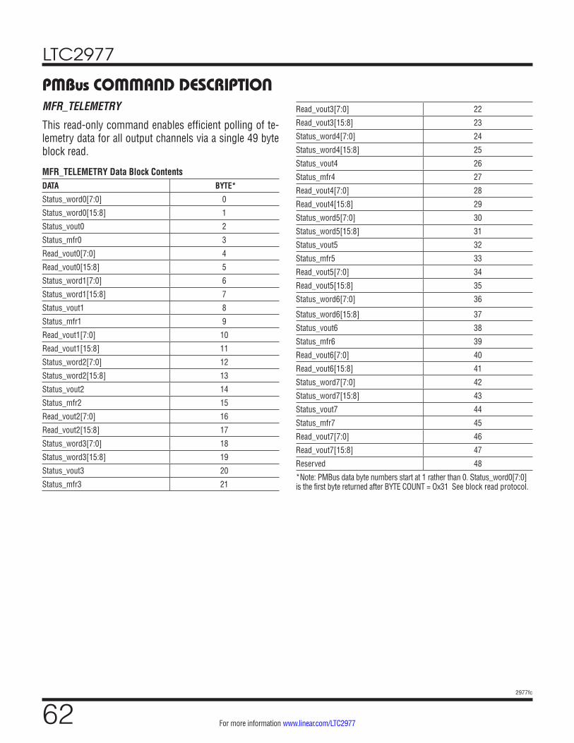
LTC2977
622977fc
For more information www.linear.com/LTC2977
PMBus COMMAND DESCRIPTIONMFR_TELEMETRY
This read-only command enables efficient polling of te-lemetry data for all output channels via a single 49 byte block read.
MFR_TELEMETRY Data Block ContentsDATA BYTE*
Status_word0[7:0] 0
Status_word0[15:8] 1
Status_vout0 2
Status_mfr0 3
Read_vout0[7:0] 4
Read_vout0[15:8] 5
Status_word1[7:0] 6
Status_word1[15:8] 7
Status_vout1 8
Status_mfr1 9
Read_vout1[7:0] 10
Read_vout1[15:8] 11
Status_word2[7:0] 12
Status_word2[15:8] 13
Status_vout2 14
Status_mfr2 15
Read_vout2[7:0] 16
Read_vout2[15:8] 17
Status_word3[7:0] 18
Status_word3[15:8] 19
Status_vout3 20
Status_mfr3 21
Read_vout3[7:0] 22
Read_vout3[15:8] 23
Status_word4[7:0] 24
Status_word4[15:8] 25
Status_vout4 26
Status_mfr4 27
Read_vout4[7:0] 28
Read_vout4[15:8] 29
Status_word5[7:0] 30
Status_word5[15:8] 31
Status_vout5 32
Status_mfr5 33
Read_vout5[7:0] 34
Read_vout5[15:8] 35
Status_word6[7:0] 36
Status_word6[15:8] 37
Status_vout6 38
Status_mfr6 39
Read_vout6[7:0] 40
Read_vout6[15:8] 41
Status_word7[7:0] 42
Status_word7[15:8] 43
Status_vout7 44
Status_mfr7 45
Read_vout7[7:0] 46
Read_vout7[15:8] 47
Reserved 48
*Note: PMBus data byte numbers start at 1 rather than 0. Status_word0[7:0] is the first byte returned after BYTE COUNT = Ox31 See block read protocol.
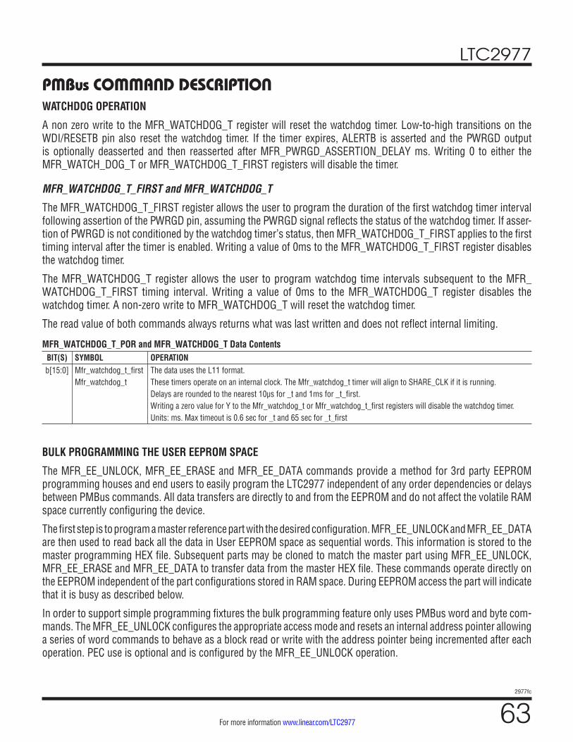
LTC2977
632977fc
For more information www.linear.com/LTC2977
WATCHDOG OPERATION
A non zero write to the MFR_WATCHDOG_T register will reset the watchdog timer. Low-to-high transitions on the WDI/RESETB pin also reset the watchdog timer. If the timer expires, ALERTB is asserted and the PWRGD output is optionally deasserted and then reasserted after MFR_PWRGD_ASSERTION_DELAY ms. Writing 0 to either the MFR_WATCH_DOG_T or MFR_WATCHDOG_T_FIRST registers will disable the timer.
MFR_WATCHDOG_T_FIRST and MFR_WATCHDOG_T
The MFR_WATCHDOG_T_FIRST register allows the user to program the duration of the first watchdog timer interval following assertion of the PWRGD pin, assuming the PWRGD signal reflects the status of the watchdog timer. If asser-tion of PWRGD is not conditioned by the watchdog timer’s status, then MFR_WATCHDOG_T_FIRST applies to the first timing interval after the timer is enabled. Writing a value of 0ms to the MFR_WATCHDOG_T_FIRST register disables the watchdog timer.
The MFR_WATCHDOG_T register allows the user to program watchdog time intervals subsequent to the MFR_WATCHDOG_T_FIRST timing interval. Writing a value of 0ms to the MFR_WATCHDOG_T register disables the watchdog timer. A non-zero write to MFR_WATCHDOG_T will reset the watchdog timer.
The read value of both commands always returns what was last written and does not reflect internal limiting.
MFR_WATCHDOG_T_POR and MFR_WATCHDOG_T Data ContentsBIT(S) SYMBOL OPERATIONb[15:0] Mfr_watchdog_t_first
Mfr_watchdog_tThe data uses the L11 format.These timers operate on an internal clock. The Mfr_watchdog_t timer will align to SHARE_CLK if it is running.Delays are rounded to the nearest 10µs for _t and 1ms for _t_first.Writing a zero value for Y to the Mfr_watchdog_t or Mfr_watchdog_t_first registers will disable the watchdog timer.Units: ms. Max timeout is 0.6 sec for _t and 65 sec for _t_first
BULK PROGRAMMING THE USER EEPROM SPACE
The MFR_EE_UNLOCK, MFR_EE_ERASE and MFR_EE_DATA commands provide a method for 3rd party EEPROM programming houses and end users to easily program the LTC2977 independent of any order dependencies or delays between PMBus commands. All data transfers are directly to and from the EEPROM and do not affect the volatile RAM space currently configuring the device.
The first step is to program a master reference part with the desired configuration. MFR_EE_UNLOCK and MFR_EE_DATA are then used to read back all the data in User EEPROM space as sequential words. This information is stored to the master programming HEX file. Subsequent parts may be cloned to match the master part using MFR_EE_UNLOCK, MFR_EE_ERASE and MFR_EE_DATA to transfer data from the master HEX file. These commands operate directly on the EEPROM independent of the part configurations stored in RAM space. During EEPROM access the part will indicate that it is busy as described below.
In order to support simple programming fixtures the bulk programming feature only uses PMBus word and byte com-mands. The MFR_EE_UNLOCK configures the appropriate access mode and resets an internal address pointer allowing a series of word commands to behave as a block read or write with the address pointer being incremented after each operation. PEC use is optional and is configured by the MFR_EE_UNLOCK operation.
PMBus COMMAND DESCRIPTION
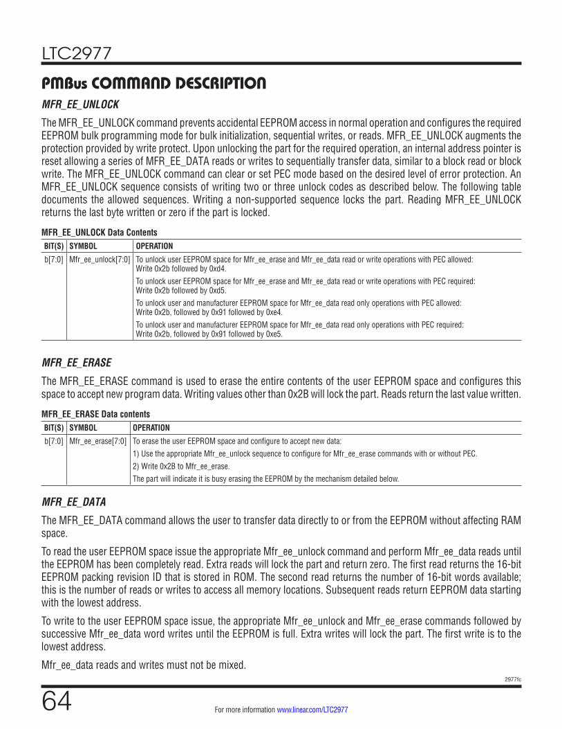
LTC2977
642977fc
For more information www.linear.com/LTC2977
PMBus COMMAND DESCRIPTIONMFR_EE_UNLOCK
The MFR_EE_UNLOCK command prevents accidental EEPROM access in normal operation and configures the required EEPROM bulk programming mode for bulk initialization, sequential writes, or reads. MFR_EE_UNLOCK augments the protection provided by write protect. Upon unlocking the part for the required operation, an internal address pointer is reset allowing a series of MFR_EE_DATA reads or writes to sequentially transfer data, similar to a block read or block write. The MFR_EE_UNLOCK command can clear or set PEC mode based on the desired level of error protection. An MFR_EE_UNLOCK sequence consists of writing two or three unlock codes as described below. The following table documents the allowed sequences. Writing a non-supported sequence locks the part. Reading MFR_EE_UNLOCK returns the last byte written or zero if the part is locked.
MFR_EE_UNLOCK Data ContentsBIT(S) SYMBOL OPERATION
b[7:0] Mfr_ee_unlock[7:0] To unlock user EEPROM space for Mfr_ee_erase and Mfr_ee_data read or write operations with PEC allowed: Write 0x2b followed by 0xd4.To unlock user EEPROM space for Mfr_ee_erase and Mfr_ee_data read or write operations with PEC required: Write 0x2b followed by 0xd5.To unlock user and manufacturer EEPROM space for Mfr_ee_data read only operations with PEC allowed: Write 0x2b, followed by 0x91 followed by 0xe4.To unlock user and manufacturer EEPROM space for Mfr_ee_data read only operations with PEC required: Write 0x2b, followed by 0x91 followed by 0xe5.
MFR_EE_ERASE
The MFR_EE_ERASE command is used to erase the entire contents of the user EEPROM space and configures this space to accept new program data. Writing values other than 0x2B will lock the part. Reads return the last value written.
MFR_EE_ERASE Data contentsBIT(S) SYMBOL OPERATION
b[7:0] Mfr_ee_erase[7:0] To erase the user EEPROM space and configure to accept new data:1) Use the appropriate Mfr_ee_unlock sequence to configure for Mfr_ee_erase commands with or without PEC.2) Write 0x2B to Mfr_ee_erase.The part will indicate it is busy erasing the EEPROM by the mechanism detailed below.
MFR_EE_DATA
The MFR_EE_DATA command allows the user to transfer data directly to or from the EEPROM without affecting RAM space.
To read the user EEPROM space issue the appropriate Mfr_ee_unlock command and perform Mfr_ee_data reads until the EEPROM has been completely read. Extra reads will lock the part and return zero. The first read returns the 16-bit EEPROM packing revision ID that is stored in ROM. The second read returns the number of 16-bit words available; this is the number of reads or writes to access all memory locations. Subsequent reads return EEPROM data starting with the lowest address.
To write to the user EEPROM space issue, the appropriate Mfr_ee_unlock and Mfr_ee_erase commands followed by successive Mfr_ee_data word writes until the EEPROM is full. Extra writes will lock the part. The first write is to the lowest address.
Mfr_ee_data reads and writes must not be mixed.
LTC2977
652977fc
For more information www.linear.com/LTC2977
MFR_EE_DATA Data ContentsBIT(S) SYMBOL OPERATION
b[15:0] Mfr_ee_data[15:0] To read user space1) Use the appropriate Mfr_ee_unlock sequence to configure for Mfr_ee_data commands with or without PEC.2) Read Mfr_ee_data[0] = PackingId (MFR Specific ID).3) Read Mfr_ee_data[1] = NumberOfUserWords (total number of 16-bit word available).4) Read Mfr_ee_data[2] through Mfr_ee_data[NumberOfUserWords+1] (User EEPROM data contents)To write user space1) Initialize the user memory using the sequence described for the MFR_EE_ERASE command.2) Use the appropriate Mfr_ee_unlock sequence to configure for Mfr_ee_data commands with or without PEC.3) Write Mfr_ee_data[0] through Mfr_ee_data[NumberOfUserWords-1] (User EEPROM data content to be written)The part will indicate it is busy erasing the EEPROM by the mechanism detailed below.
Response When Part Is Busy
The part will indicate it is busy accessing the EEPROM by the following mechanism:
1) Clearing Mfr_common_busyb of the MFR_COMMON register. This byte can always be read and will never NACK a byte read request even if the part is busy.
2) NACKing commands other than MFR_COMMON.
MFR_EE Erase and Write Programming Time
The program time per word is typically 0.17ms and will require spacing the I2C/SMBus writes at greater than 0.17ms to guarantee the write has completed. The Mfr_ee_erase command takes approximately 400ms. We recommend using MFR_COMMON for handshaking.
FAULT LOG OPERATION
A conceptual diagram of the fault log is shown in Figure 14. The fault log provides black box capability to the LTC2977. During normal operation the contents of the status registers, the output voltage readings, temperature readings as well as peak and min values of these quantities are stored in a continuously updated buffer in RAM. You can think of the operation as being similar to a strip chart recorder. When a fault occurs, the contents are written into EEPROM for nonvolatile storage. The EEPROM fault log is then locked. The part can be powered down with the fault log available for reading at a later time.
MFR_FAULT_LOG_STORE
This command allows the user to transfer data from the RAM buffer to EEPROM.
MFR_FAULT_LOG_RESTORE
This command allows the user to transfer a copy of the fault-log data from the EEPROM to the RAM buffer. After a restore the RAM buffer is locked until a successful MFR_FAULT_LOG read or MFR_FAULT_LOG_CLEAR.
PMBus COMMAND DESCRIPTION
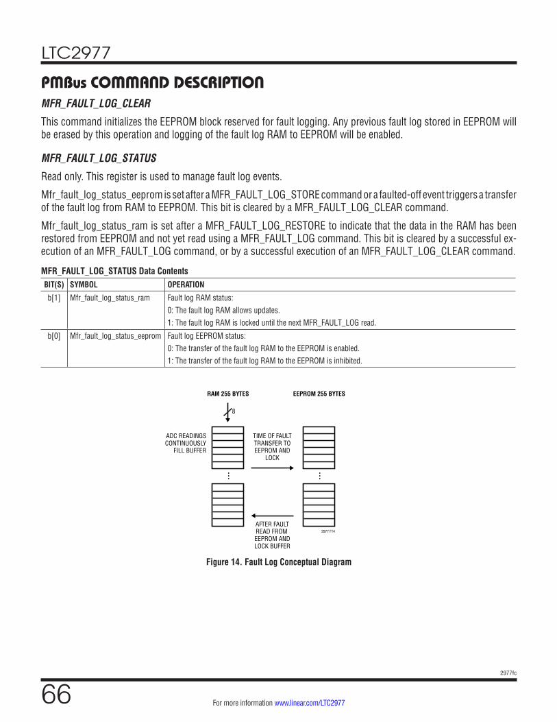
LTC2977
662977fc
For more information www.linear.com/LTC2977
PMBus COMMAND DESCRIPTIONMFR_FAULT_LOG_CLEAR
This command initializes the EEPROM block reserved for fault logging. Any previous fault log stored in EEPROM will be erased by this operation and logging of the fault log RAM to EEPROM will be enabled.
MFR_FAULT_LOG_STATUS
Read only. This register is used to manage fault log events.
Mfr_fault_log_status_eeprom is set after a MFR_FAULT_LOG_STORE command or a faulted-off event triggers a transfer of the fault log from RAM to EEPROM. This bit is cleared by a MFR_FAULT_LOG_CLEAR command.
Mfr_fault_log_status_ram is set after a MFR_FAULT_LOG_RESTORE to indicate that the data in the RAM has been restored from EEPROM and not yet read using a MFR_FAULT_LOG command. This bit is cleared by a successful ex-ecution of an MFR_FAULT_LOG command, or by a successful execution of an MFR_FAULT_LOG_CLEAR command.
MFR_FAULT_LOG_STATUS Data ContentsBIT(S) SYMBOL OPERATION
b[1] Mfr_fault_log_status_ram Fault log RAM status:0: The fault log RAM allows updates.1: The fault log RAM is locked until the next MFR_FAULT_LOG read.
b[0] Mfr_fault_log_status_eeprom Fault log EEPROM status:0: The transfer of the fault log RAM to the EEPROM is enabled.1: The transfer of the fault log RAM to the EEPROM is inhibited.
Figure 14. Fault Log Conceptual Diagram
2977 F14
ADC READINGSCONTINUOUSLY
FILL BUFFER
TIME OF FAULTTRANSFER TOEEPROM AND
LOCK
AFTER FAULTREAD FROM EEPROM ANDLOCK BUFFER
RAM 255 BYTES EEPROM 255 BYTES
8
... ...
LTC2977
672977fc
For more information www.linear.com/LTC2977
PMBus COMMAND DESCRIPTIONMFR_FAULT_LOG
Read only. This 2040-bit (255 byte) data block contains a copy of the RAM buffer fault log. The RAM buffer is continu-ously updated after each ADC conversion as long as Mfr_fault_log_status_ram is clear.
With Mfr_config_all_fault_log_enable = 1 and Mfr_fault_log_status_eeprom = 0, the RAM buffer is transferred to EE-PROM whenever an LTC2977 fault causes a channel to latch off or a MFR_FAULT_LOG_STORE command is received. This transfer is delayed until the ADC has updated its READ values for all channels when Mfr_config_all_fast_fault_log is clear, otherwise it happens within 24ms. This optional delay can be used to ensure that the slower, ADC monitored, values are all updated for the case where a fast supervisor detected fault initiates the transfer to EEPROM.
Mfr_fault_log_status_eeprom is set high after the RAM buffer is transferred to EEPROM and not cleared until a MFR_FAULT_LOG_CLEAR is received, even if the LTC2977 is reset or powered down. Fault log EEPROM transfers are not initiated as a result of Status_mfr_discharge events.
During a MFR_FAULT_LOG read, data is returned as defined by the following table. The fault log data is partitioned into two sections. The first section is referred to as the preamble and contains the Position-last pointer, time information and peak and minimum values. The second section contains a chronological record of telemetry and requires Position-last for proper interpretation. The fault log stores approximately 0.5 seconds of telemetry. To prevent timeouts during block reads, it is recommended that Mfr_config_all_longer_pmbus_timeout be set to 1.
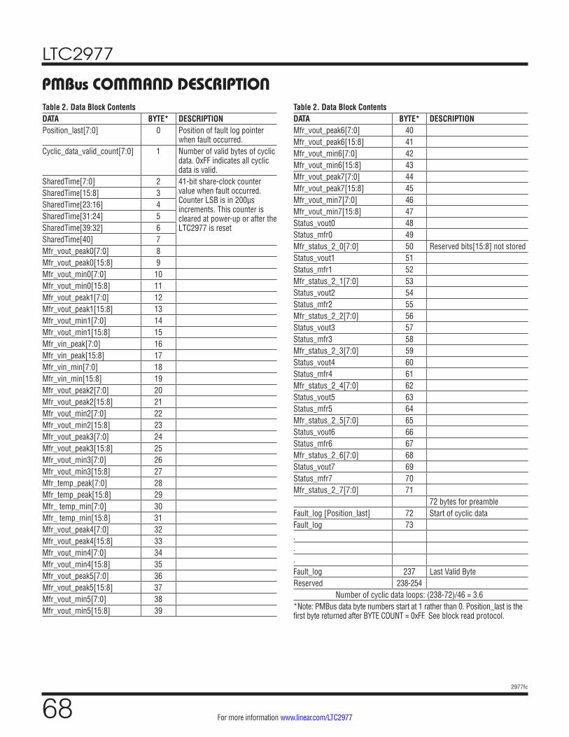
LTC2977
682977fc
For more information www.linear.com/LTC2977
Table 2. Data Block ContentsDATA BYTE* DESCRIPTIONMfr_vout_peak6[7:0] 40Mfr_vout_peak6[15:8] 41Mfr_vout_min6[7:0] 42Mfr_vout_min6[15:8] 43Mfr_vout_peak7[7:0] 44Mfr_vout_peak7[15:8] 45Mfr_vout_min7[7:0] 46Mfr_vout_min7[15:8] 47Status_vout0 48Status_mfr0 49Mfr_status_2_0[7:0] 50 Reserved bits[15:8] not storedStatus_vout1 51Status_mfr1 52Mfr_status_2_1[7:0] 53Status_vout2 54Status_mfr2 55Mfr_status_2_2[7:0] 56Status_vout3 57Status_mfr3 58Mfr_status_2_3[7:0] 59Status_vout4 60Status_mfr4 61Mfr_status_2_4[7:0] 62Status_vout5 63Status_mfr5 64Mfr_status_2_5[7:0] 65Status_vout6 66Status_mfr6 67Mfr_status_2_6[7:0] 68Status_vout7 69Status_mfr7 70Mfr_status_2_7[7:0] 71
72 bytes for preambleFault_log [Position_last] 72 Start of cyclic dataFault_log 73...Fault_log 237 Last Valid ByteReserved 238-254
Number of cyclic data loops: (238-72)/46 = 3.6*Note: PMBus data byte numbers start at 1 rather than 0. Position_last is the first byte returned after BYTE COUNT = 0xFF. See block read protocol.
PMBus COMMAND DESCRIPTIONTable 2. Data Block ContentsDATA BYTE* DESCRIPTIONPosition_last[7:0] 0 Position of fault log pointer
when fault occurred. Cyclic_data_valid_count[7:0] 1 Number of valid bytes of cyclic
data. 0xFF indicates all cyclic data is valid.
SharedTime[7:0] 2 41-bit share-clock counter value when fault occurred. Counter LSB is in 200µs increments. This counter is cleared at power-up or after the LTC2977 is reset
SharedTime[15:8] 3SharedTime[23:16] 4SharedTime[31:24] 5SharedTime[39:32] 6SharedTime[40] 7Mfr_vout_peak0[7:0] 8Mfr_vout_peak0[15:8] 9Mfr_vout_min0[7:0] 10Mfr_vout_min0[15:8] 11Mfr_vout_peak1[7:0] 12Mfr_vout_peak1[15:8] 13Mfr_vout_min1[7:0] 14Mfr_vout_min1[15:8] 15Mfr_vin_peak[7:0] 16Mfr_vin_peak[15:8] 17Mfr_vin_min[7:0] 18Mfr_vin_min[15:8] 19Mfr_vout_peak2[7:0] 20Mfr_vout_peak2[15:8] 21Mfr_vout_min2[7:0] 22Mfr_vout_min2[15:8] 23Mfr_vout_peak3[7:0] 24Mfr_vout_peak3[15:8] 25Mfr_vout_min3[7:0] 26Mfr_vout_min3[15:8] 27Mfr_temp_peak[7:0] 28Mfr_temp_peak[15:8] 29Mfr_ temp_min[7:0] 30Mfr_ temp_min[15:8] 31Mfr_vout_peak4[7:0] 32Mfr_vout_peak4[15:8] 33Mfr_vout_min4[7:0] 34Mfr_vout_min4[15:8] 35Mfr_vout_peak5[7:0] 36Mfr_vout_peak5[15:8] 37Mfr_vout_min5[7:0] 38Mfr_vout_min5[15:8] 39

LTC2977
692977fc
For more information www.linear.com/LTC2977
The data returned between bytes 72 and 237 of the previous table is interpreted using Position_last and the following table. The key to identifying byte 72 is to locate the DATA corresponding to POSITION = Position_last in the next table. Subsequent bytes are identified by decrementing the value of POSITION. For example: If Position_last = 11 then the first data returned in byte position 72 of a block read is Read_vin[15:8] followed by Read_vin[7:0] followed by Mfr_status_2 of page 1. See Table 3.
Table 3. Interpreting Cyclical LoopPOSITION DATA
0 Read_vout0[7:0]1 Read_vout0[15:8]2 Status_vout03 Status_mfr04 Mfr_status_2_0[7:0]5 Read_vout1[7:0]6 Read_vout1[15:8]7 Status_vout18 Status_mfr19 Mfr_status_2_1[7:0]10 Read_vin[7:0]11 Read_vin[15:8]12 Status_vin13 Read_vout2[7:0]14 Read_vout2[15:8]15 Status_vout216 Status_mfr217 Mfr_status_2_2[7:0]18 Read_vout3[7:0]19 Read_vout3[15:8]20 Status_vout321 Status_mfr322 Mfr_status_2_3[7:0]23 Read_temperature_1[7:0]24 Read_temperature_1[15:8]25 Status_temp26 Read_vout4[7:0]27 Read_vout4[15:8]28 Status_vout429 Status_mfr430 Mfr_status_2_4[7:0]31 Read_vout5[7:0]32 Read_vout5[15:8]33 Status_vout5
Table 3. Interpreting Cyclical LoopPOSITION DATA
34 Status_mfr535 Mfr_status_2_5[7:0]36 Read_vout6[7:0]37 Read_vout6[15:8]38 Status_vout639 Status_mfr640 Mfr_status_2_6[7:0]41 Read_vout7[7:0]42 Read_vout7[15:8]43 Status_vout744 Status_mfr745 Mfr_status_2_7[7:0]
Total Bytes = 46
The following table fully decodes a sample fault log read to help clarify the cyclical nature of the operation.MFR_FAULT_LOG DATA BLOCK CONTENTS
PREAMBLE INFORMATION
BYTE NUMBER DECIMAL
BYTE NUMBER
HEX DATA DESCRIPTION
0 00 Position_last[7:0] = 11 Position of Fault-Log Pointer When Fault Occurred.
1 01 Cyclic_data_valid_count[7:0] = 160
Final 6 Bytes Of Cyclic Data Not Valid
2 02 SharedTime[7:0] 41-Bit Share-Clock Counter Value When Fault Occurred. Counter LSB Is in 200µs Increments.
3 03 SharedTime[15:8]
4 04 SharedTime[23:16]
5 05 SharedTime[31:24]
6 06 SharedTime[39:32]
7 07 SharedTime[40]
8 08 Mfr_vout_peak0[7:0]
9 09 Mfr_vout_peak0[15:8]
10 0A Mfr_vout_min0[7:0]
11 0B Mfr_vout_min0[15:8]
12 0C Mfr_vout_peak1[7:0]
13 0D Mfr_vout_peak1[15:8]
14 0E Mfr_vout_min1[7:0]
15 0F Mfr_vout_min1[15:8]
PMBus COMMAND DESCRIPTION
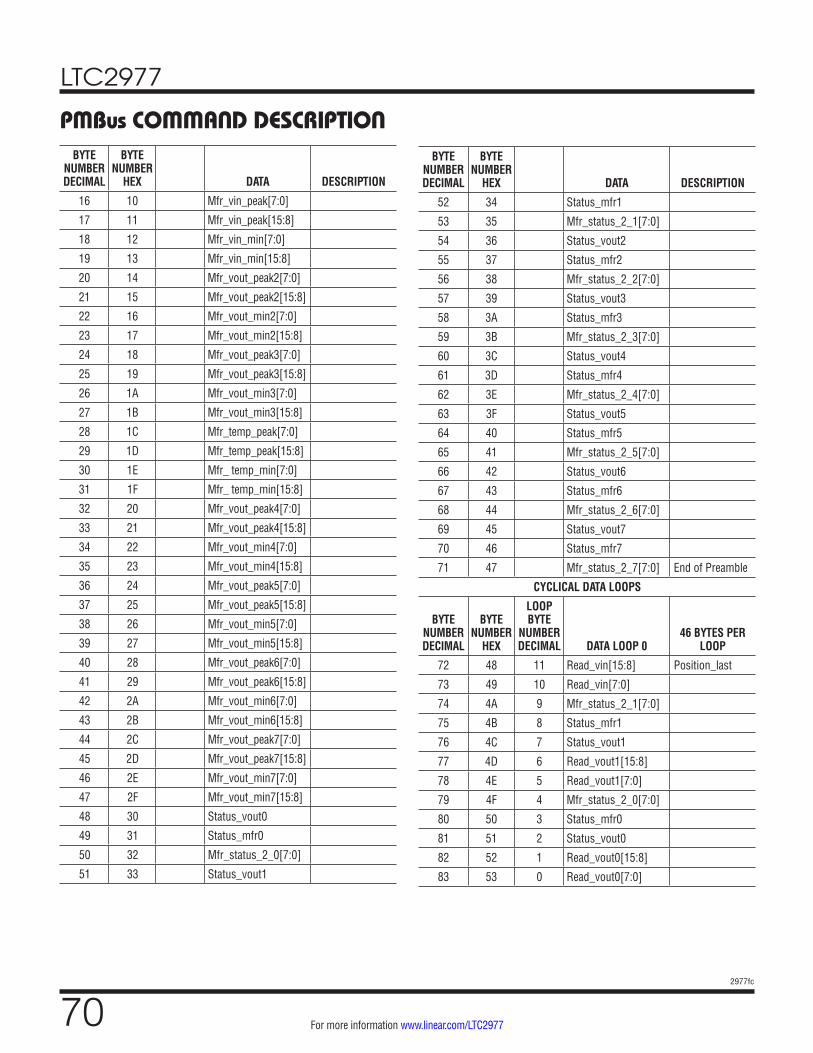
LTC2977
702977fc
For more information www.linear.com/LTC2977
BYTE NUMBER DECIMAL
BYTE NUMBER
HEX DATA DESCRIPTION
16 10 Mfr_vin_peak[7:0]
17 11 Mfr_vin_peak[15:8]
18 12 Mfr_vin_min[7:0]
19 13 Mfr_vin_min[15:8]
20 14 Mfr_vout_peak2[7:0]
21 15 Mfr_vout_peak2[15:8]
22 16 Mfr_vout_min2[7:0]
23 17 Mfr_vout_min2[15:8]
24 18 Mfr_vout_peak3[7:0]
25 19 Mfr_vout_peak3[15:8]
26 1A Mfr_vout_min3[7:0]
27 1B Mfr_vout_min3[15:8]
28 1C Mfr_temp_peak[7:0]
29 1D Mfr_temp_peak[15:8]
30 1E Mfr_ temp_min[7:0]
31 1F Mfr_ temp_min[15:8]
32 20 Mfr_vout_peak4[7:0]
33 21 Mfr_vout_peak4[15:8]
34 22 Mfr_vout_min4[7:0]
35 23 Mfr_vout_min4[15:8]
36 24 Mfr_vout_peak5[7:0]
37 25 Mfr_vout_peak5[15:8]
38 26 Mfr_vout_min5[7:0]
39 27 Mfr_vout_min5[15:8]
40 28 Mfr_vout_peak6[7:0]
41 29 Mfr_vout_peak6[15:8]
42 2A Mfr_vout_min6[7:0]
43 2B Mfr_vout_min6[15:8]
44 2C Mfr_vout_peak7[7:0]
45 2D Mfr_vout_peak7[15:8]
46 2E Mfr_vout_min7[7:0]
47 2F Mfr_vout_min7[15:8]
48 30 Status_vout0
49 31 Status_mfr0
50 32 Mfr_status_2_0[7:0]
51 33 Status_vout1
BYTE NUMBER DECIMAL
BYTE NUMBER
HEX DATA DESCRIPTION
52 34 Status_mfr1
53 35 Mfr_status_2_1[7:0]
54 36 Status_vout2
55 37 Status_mfr2
56 38 Mfr_status_2_2[7:0]
57 39 Status_vout3
58 3A Status_mfr3
59 3B Mfr_status_2_3[7:0]
60 3C Status_vout4
61 3D Status_mfr4
62 3E Mfr_status_2_4[7:0]
63 3F Status_vout5
64 40 Status_mfr5
65 41 Mfr_status_2_5[7:0]
66 42 Status_vout6
67 43 Status_mfr6
68 44 Mfr_status_2_6[7:0]
69 45 Status_vout7
70 46 Status_mfr7
71 47 Mfr_status_2_7[7:0] End of Preamble
CYCLICAL DATA LOOPS
BYTE NUMBER DECIMAL
BYTE NUMBER
HEX
LOOP BYTE
NUMBER DECIMAL DATA LOOP 0
46 BYTES PER LOOP
72 48 11 Read_vin[15:8] Position_last
73 49 10 Read_vin[7:0]
74 4A 9 Mfr_status_2_1[7:0]
75 4B 8 Status_mfr1
76 4C 7 Status_vout1
77 4D 6 Read_vout1[15:8]
78 4E 5 Read_vout1[7:0]
79 4F 4 Mfr_status_2_0[7:0]
80 50 3 Status_mfr0
81 51 2 Status_vout0
82 52 1 Read_vout0[15:8]
83 53 0 Read_vout0[7:0]
PMBus COMMAND DESCRIPTION
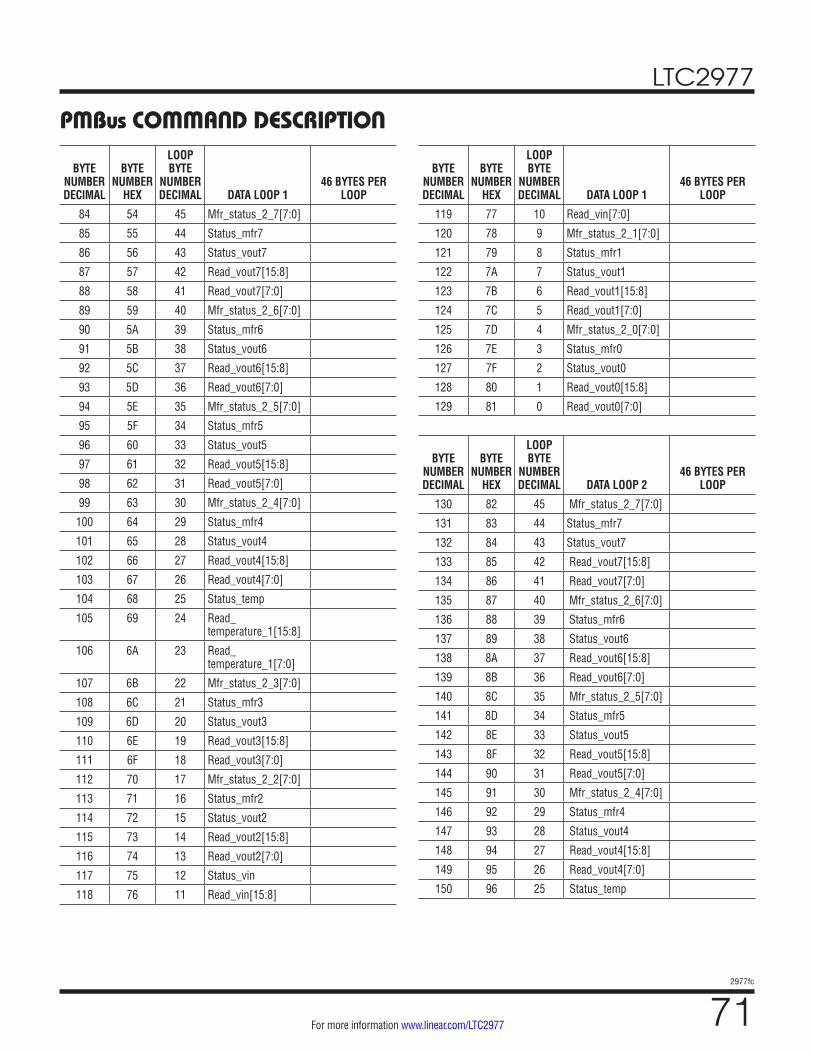
LTC2977
712977fc
For more information www.linear.com/LTC2977
BYTE NUMBER DECIMAL
BYTE NUMBER
HEX
LOOP BYTE
NUMBER DECIMAL DATA LOOP 1
46 BYTES PER LOOP
84 54 45 Mfr_status_2_7[7:0]
85 55 44 Status_mfr7
86 56 43 Status_vout7
87 57 42 Read_vout7[15:8]
88 58 41 Read_vout7[7:0]
89 59 40 Mfr_status_2_6[7:0]
90 5A 39 Status_mfr6
91 5B 38 Status_vout6
92 5C 37 Read_vout6[15:8]
93 5D 36 Read_vout6[7:0]
94 5E 35 Mfr_status_2_5[7:0]
95 5F 34 Status_mfr5
96 60 33 Status_vout5
97 61 32 Read_vout5[15:8]
98 62 31 Read_vout5[7:0]
99 63 30 Mfr_status_2_4[7:0]
100 64 29 Status_mfr4
101 65 28 Status_vout4
102 66 27 Read_vout4[15:8]
103 67 26 Read_vout4[7:0]
104 68 25 Status_temp
105 69 24 Read_ temperature_1[15:8]
106 6A 23 Read_ temperature_1[7:0]
107 6B 22 Mfr_status_2_3[7:0]
108 6C 21 Status_mfr3
109 6D 20 Status_vout3
110 6E 19 Read_vout3[15:8]
111 6F 18 Read_vout3[7:0]
112 70 17 Mfr_status_2_2[7:0]
113 71 16 Status_mfr2
114 72 15 Status_vout2
115 73 14 Read_vout2[15:8]
116 74 13 Read_vout2[7:0]
117 75 12 Status_vin
118 76 11 Read_vin[15:8]
BYTE NUMBER DECIMAL
BYTE NUMBER
HEX
LOOP BYTE
NUMBER DECIMAL DATA LOOP 1
46 BYTES PER LOOP
119 77 10 Read_vin[7:0]
120 78 9 Mfr_status_2_1[7:0]
121 79 8 Status_mfr1
122 7A 7 Status_vout1
123 7B 6 Read_vout1[15:8]
124 7C 5 Read_vout1[7:0]
125 7D 4 Mfr_status_2_0[7:0]
126 7E 3 Status_mfr0
127 7F 2 Status_vout0
128 80 1 Read_vout0[15:8]
129 81 0 Read_vout0[7:0]
BYTE NUMBER DECIMAL
BYTE NUMBER
HEX
LOOP BYTE
NUMBER DECIMAL DATA LOOP 2
46 BYTES PER LOOP
130 82 45 Mfr_status_2_7[7:0]
131 83 44 Status_mfr7
132 84 43 Status_vout7
133 85 42 Read_vout7[15:8]
134 86 41 Read_vout7[7:0]
135 87 40 Mfr_status_2_6[7:0]
136 88 39 Status_mfr6
137 89 38 Status_vout6
138 8A 37 Read_vout6[15:8]
139 8B 36 Read_vout6[7:0]
140 8C 35 Mfr_status_2_5[7:0]
141 8D 34 Status_mfr5
142 8E 33 Status_vout5
143 8F 32 Read_vout5[15:8]
144 90 31 Read_vout5[7:0]
145 91 30 Mfr_status_2_4[7:0]
146 92 29 Status_mfr4
147 93 28 Status_vout4
148 94 27 Read_vout4[15:8]
149 95 26 Read_vout4[7:0]
150 96 25 Status_temp
PMBus COMMAND DESCRIPTION
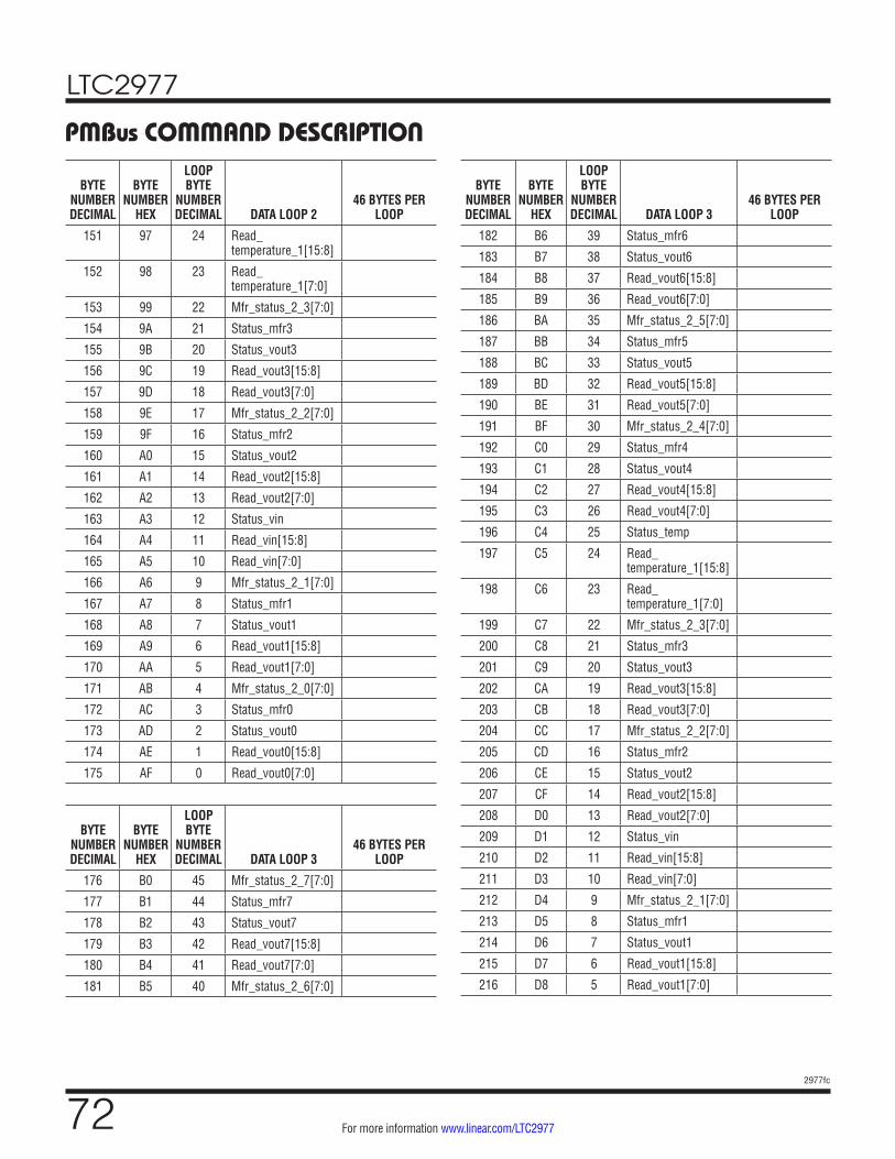
LTC2977
722977fc
For more information www.linear.com/LTC2977
PMBus COMMAND DESCRIPTION
BYTE NUMBER DECIMAL
BYTE NUMBER
HEX
LOOP BYTE
NUMBER DECIMAL DATA LOOP 2
46 BYTES PER LOOP
151 97 24 Read_temperature_1[15:8]
152 98 23 Read_temperature_1[7:0]
153 99 22 Mfr_status_2_3[7:0]
154 9A 21 Status_mfr3
155 9B 20 Status_vout3
156 9C 19 Read_vout3[15:8]
157 9D 18 Read_vout3[7:0]
158 9E 17 Mfr_status_2_2[7:0]
159 9F 16 Status_mfr2
160 A0 15 Status_vout2
161 A1 14 Read_vout2[15:8]
162 A2 13 Read_vout2[7:0]
163 A3 12 Status_vin
164 A4 11 Read_vin[15:8]
165 A5 10 Read_vin[7:0]
166 A6 9 Mfr_status_2_1[7:0]
167 A7 8 Status_mfr1
168 A8 7 Status_vout1
169 A9 6 Read_vout1[15:8]
170 AA 5 Read_vout1[7:0]
171 AB 4 Mfr_status_2_0[7:0]
172 AC 3 Status_mfr0
173 AD 2 Status_vout0
174 AE 1 Read_vout0[15:8]
175 AF 0 Read_vout0[7:0]
BYTE NUMBER DECIMAL
BYTE NUMBER
HEX
LOOP BYTE
NUMBER DECIMAL DATA LOOP 3
46 BYTES PER LOOP
176 B0 45 Mfr_status_2_7[7:0]
177 B1 44 Status_mfr7
178 B2 43 Status_vout7
179 B3 42 Read_vout7[15:8]
180 B4 41 Read_vout7[7:0]
181 B5 40 Mfr_status_2_6[7:0]
BYTE NUMBER DECIMAL
BYTE NUMBER
HEX
LOOP BYTE
NUMBER DECIMAL DATA LOOP 3
46 BYTES PER LOOP
182 B6 39 Status_mfr6
183 B7 38 Status_vout6
184 B8 37 Read_vout6[15:8]
185 B9 36 Read_vout6[7:0]
186 BA 35 Mfr_status_2_5[7:0]
187 BB 34 Status_mfr5
188 BC 33 Status_vout5
189 BD 32 Read_vout5[15:8]
190 BE 31 Read_vout5[7:0]
191 BF 30 Mfr_status_2_4[7:0]
192 C0 29 Status_mfr4
193 C1 28 Status_vout4
194 C2 27 Read_vout4[15:8]
195 C3 26 Read_vout4[7:0]
196 C4 25 Status_temp
197 C5 24 Read_temperature_1[15:8]
198 C6 23 Read_temperature_1[7:0]
199 C7 22 Mfr_status_2_3[7:0]
200 C8 21 Status_mfr3
201 C9 20 Status_vout3
202 CA 19 Read_vout3[15:8]
203 CB 18 Read_vout3[7:0]
204 CC 17 Mfr_status_2_2[7:0]
205 CD 16 Status_mfr2
206 CE 15 Status_vout2
207 CF 14 Read_vout2[15:8]
208 D0 13 Read_vout2[7:0]
209 D1 12 Status_vin
210 D2 11 Read_vin[15:8]
211 D3 10 Read_vin[7:0]
212 D4 9 Mfr_status_2_1[7:0]
213 D5 8 Status_mfr1
214 D6 7 Status_vout1
215 D7 6 Read_vout1[15:8]
216 D8 5 Read_vout1[7:0]
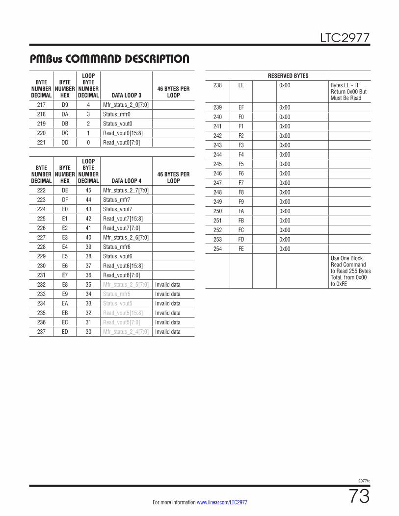
LTC2977
732977fc
For more information www.linear.com/LTC2977
BYTE NUMBER DECIMAL
BYTE NUMBER
HEX
LOOP BYTE
NUMBER DECIMAL DATA LOOP 3
46 BYTES PER LOOP
217 D9 4 Mfr_status_2_0[7:0]
218 DA 3 Status_mfr0
219 DB 2 Status_vout0
220 DC 1 Read_vout0[15:8]
221 DD 0 Read_vout0[7:0]
BYTE NUMBER DECIMAL
BYTE NUMBER
HEX
LOOP BYTE
NUMBER DECIMAL DATA LOOP 4
46 BYTES PER LOOP
222 DE 45 Mfr_status_2_7[7:0]
223 DF 44 Status_mfr7
224 E0 43 Status_vout7
225 E1 42 Read_vout7[15:8]
226 E2 41 Read_vout7[7:0]
227 E3 40 Mfr_status_2_6[7:0]
228 E4 39 Status_mfr6
229 E5 38 Status_vout6
230 E6 37 Read_vout6[15:8]
231 E7 36 Read_vout6[7:0]
232 E8 35 Mfr_status_2_5[7:0] Invalid data
233 E9 34 Status_mfr5 Invalid data
234 EA 33 Status_vout5 Invalid data
235 EB 32 Read_vout5[15:8] Invalid data
236 EC 31 Read_vout5[7:0] Invalid data
237 ED 30 Mfr_status_2_4[7:0] Invalid data
RESERVED BYTES
238 EE 0x00 Bytes EE - FE Return 0x00 But Must Be Read
239 EF 0x00
240 F0 0x00
241 F1 0x00
242 F2 0x00
243 F3 0x00
244 F4 0x00
245 F5 0x00
246 F6 0x00
247 F7 0x00
248 F8 0x00
249 F9 0x00
250 FA 0x00
251 FB 0x00
252 FC 0x00
253 FD 0x00
254 FE 0x00
Use One Block Read Command to Read 255 Bytes Total, from 0x00 to 0xFE
PMBus COMMAND DESCRIPTION
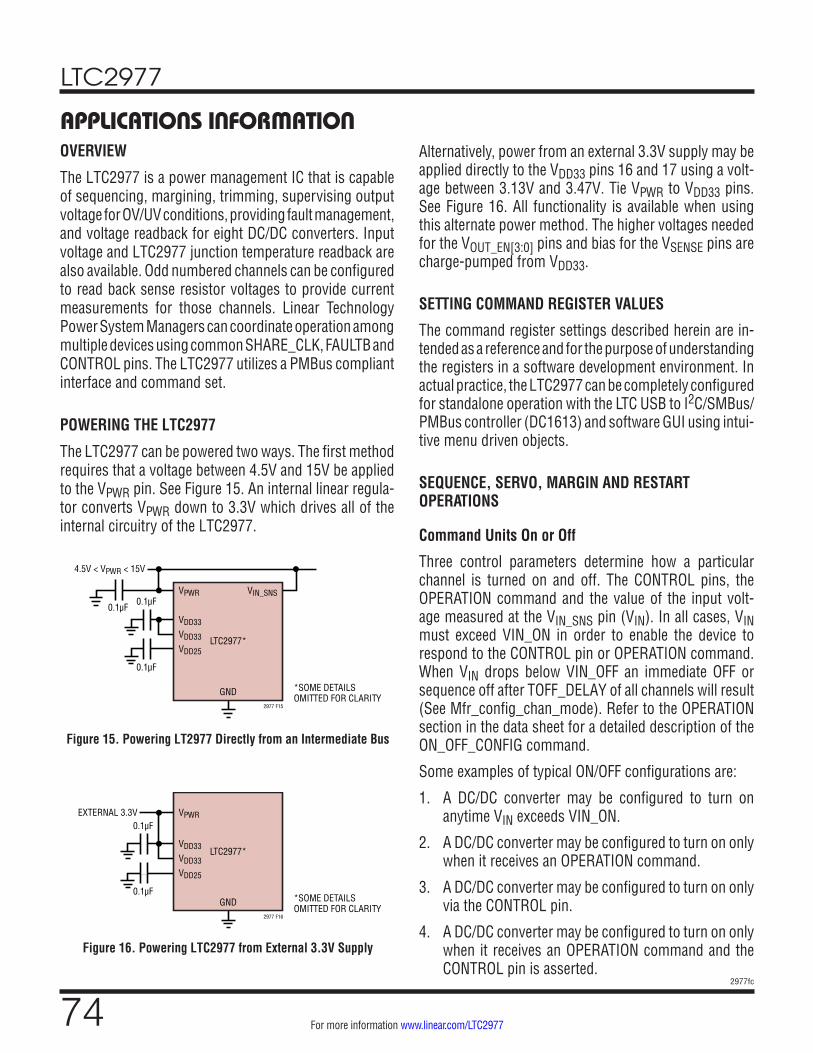
LTC2977
742977fc
For more information www.linear.com/LTC2977
APPLICATIONS INFORMATIONOVERVIEW
The LTC2977 is a power management IC that is capable of sequencing, margining, trimming, supervising output voltage for OV/UV conditions, providing fault management, and voltage readback for eight DC/DC converters. Input voltage and LTC2977 junction temperature readback are also available. Odd numbered channels can be configured to read back sense resistor voltages to provide current measurements for those channels. Linear Technology Power System Managers can coordinate operation among multiple devices using common SHARE_CLK, FAULTB and CONTROL pins. The LTC2977 utilizes a PMBus compliant interface and command set.
POWERING THE LTC2977
The LTC2977 can be powered two ways. The first method requires that a voltage between 4.5V and 15V be applied to the VPWR pin. See Figure 15. An internal linear regula-tor converts VPWR down to 3.3V which drives all of the internal circuitry of the LTC2977.
Alternatively, power from an external 3.3V supply may be applied directly to the VDD33 pins 16 and 17 using a volt-age between 3.13V and 3.47V. Tie VPWR to VDD33 pins. See Figure 16. All functionality is available when using this alternate power method. The higher voltages needed for the VOUT_EN[3:0] pins and bias for the VSENSE pins are charge-pumped from VDD33.
SETTING COMMAND REGISTER VALUES
The command register settings described herein are in-tended as a reference and for the purpose of understanding the registers in a software development environment. In actual practice, the LTC2977 can be completely configured for standalone operation with the LTC USB to I2C/SMBus/PMBus controller (DC1613) and software GUI using intui-tive menu driven objects.
SEQUENCE, SERVO, MARGIN AND RESTART OPERATIONS
Command Units On or Off
Three control parameters determine how a particular channel is turned on and off. The CONTROL pins, the OPERATION command and the value of the input volt-age measured at the VIN_SNS pin (VIN). In all cases, VIN must exceed VIN_ON in order to enable the device to respond to the CONTROL pin or OPERATION command. When VIN drops below VIN_OFF an immediate OFF or sequence off after TOFF_DELAY of all channels will result (See Mfr_config_chan_mode). Refer to the OPERATION section in the data sheet for a detailed description of the ON_OFF_CONFIG command.
Some examples of typical ON/OFF configurations are:
1. A DC/DC converter may be configured to turn on anytime VIN exceeds VIN_ON.
2. A DC/DC converter may be configured to turn on only when it receives an OPERATION command.
3. A DC/DC converter may be configured to turn on only via the CONTROL pin.
4. A DC/DC converter may be configured to turn on only when it receives an OPERATION command and the CONTROL pin is asserted.
Figure 15. Powering LT2977 Directly from an Intermediate Bus
Figure 16. Powering LTC2977 from External 3.3V Supply
VPWR
VDD33
VDD33
VDD25
VIN_SNS
LTC2977*
0.1µF
0.1µF
4.5V < VPWR < 15V
GND
0.1µF
*SOME DETAILSOMITTED FOR CLARITY
2977 F15
VDD33
VDD33
VDD25
VPWR
LTC2977*
0.1µF
0.1µFGND *SOME DETAILS
OMITTED FOR CLARITY2977 F16
EXTERNAL 3.3V
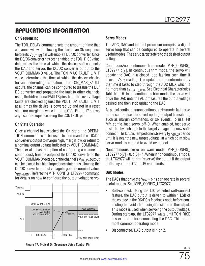
LTC2977
752977fc
For more information www.linear.com/LTC2977
APPLICATIONS INFORMATIONOn Sequencing
The TON_DELAY command sets the amount of time that a channel will wait following the start of an ON sequence before its VOUT_EN pin will enable a DC/DC converter. Once the DC/DC converter has been enabled, the TON_RISE value determines the time at which the device soft-connects the DAC and servos the DC/DC converter output to the VOUT_COMMAND value. The TON_MAX_FAULT_LIMIT value determines the time at which the device checks for an undervoltage condition. If a TON_MAX_FAULT occurs, the channel can be configured to disable the DC/DC converter and propagate the fault to other channels using the bidirectional FAULTB pins. Note that overvoltage faults are checked against the VOUT_OV_FAULT_LIMIT at all times the device is powered up and not in a reset state nor margining while ignoring OVs. Figure 17 shows a typical on-sequence using the CONTROL pin.
On State Operation
Once a channel has reached the ON state, the OPERA-TION command can be used to command the DC/DC converter’s output to margin high, margin low, or return to a nominal output voltage indicated by VOUT_COMMAND. The user also has the option of configuring a channel to continuously trim the output of the DC/DC converter to the VOUT_COMMAND voltage, or the channel’s VDACPn output can be placed in a high impedance state thus allowing the DC/DC converter output voltage to go to its nominal value, VDCn (NOM). Refer to the MFR_CONFIG_LTC2977 command for details on how to configure the output voltage servo.
Servo Modes
The ADC, DAC and internal processor comprise a digital servo loop that can be configured to operate in several useful modes. The servo target refers to the desired output voltage.
Continuous/noncontinuous trim mode. MFR_CONFIG_ LTC2977 b[7]. In continuous trim mode, the servo will update the DAC in a closed loop fashion each time it takes a VOUT reading. The update rate is determined by the time it takes to step through the ADC MUX which is no more than tUPDATE_ADC. See Electrical Characteristics Table Note 5. In noncontinuous trim mode, the servo will drive the DAC until the ADC measures the output voltage desired and then stop updating the DAC.
As part of continuous/noncontinuous trim mode, fast servo mode can be used to speed up large output transitions, such as margin commands, or ON events. To use, set Mfr_config_fast_servo_off=0. When enabled, fast servo is started by a change to the target voltage or a new soft-connect. The DAC is ramped one lsb every tS_VDACP period until it is near the new target voltage, at which point slow servo mode is entered to avoid overshoot.
Noncontinuous servo on warn mode. MFR_CONFIG_LTC2977 b[7] = 0, b[6] = 1. When in noncontinuous mode, the LTC2977 will retrim (reservo) the output if the output drifts beyond the OV or UV warn limits.
DAC Modes
The DACs that drive the VDACn pins can operate in several useful modes. See MFR_CONFIG_LTC2977.
• Soft-connect. Using the LTC patented soft-connect feature, the DAC output is driven to within 1 LSB of the voltage at the DC/DC’s feedback node before con-necting, to avoid introducing transients on the output. This mode is used when servoing the output voltage. During start-up, the LTC2977 waits until TON_RISE has expired before connecting the DAC. This is the most common operating mode.
• Disconnected. DAC output is high Z.
Figure 17. Typical On Sequence Using Control Pin
VOUT_0V_FAULT_LIMIT
DAC SOFT-CONNECTSAND BEGINS
ADJUSTING OUTPUTVOUT_UV_FAULT_LIMIT
VCONTROL
VOUT_EN
VOUT
TON_DELAY TON_RISE
2977 F17
VDC(NOM)
VOUT_COMMAND
TON_MAX_FAULT_LIMIT
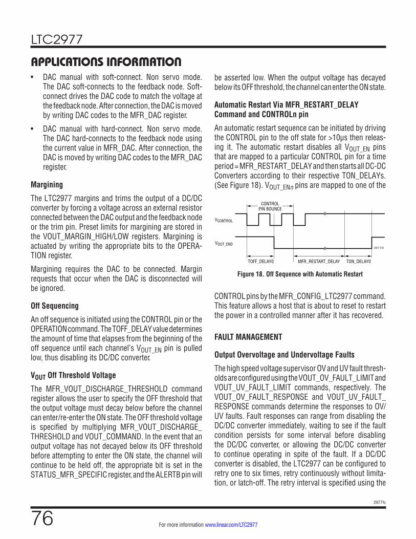
LTC2977
762977fc
For more information www.linear.com/LTC2977
• DAC manual with soft-connect. Non servo mode. The DAC soft-connects to the feedback node. Soft-connect drives the DAC code to match the voltage at the feedback node. After connection, the DAC is moved by writing DAC codes to the MFR_DAC register.
• DAC manual with hard-connect. Non servo mode. The DAC hard-connects to the feedback node using the current value in MFR_DAC. After connection, the DAC is moved by writing DAC codes to the MFR_DAC register.
Margining
The LTC2977 margins and trims the output of a DC/DC converter by forcing a voltage across an external resistor connected between the DAC output and the feedback node or the trim pin. Preset limits for margining are stored in the VOUT_MARGIN_HIGH/LOW registers. Margining is actuated by writing the appropriate bits to the OPERA-TION register.
Margining requires the DAC to be connected. Margin requests that occur when the DAC is disconnected will be ignored.
Off Sequencing
An off sequence is initiated using the CONTROL pin or the OPERATION command. The TOFF_DELAY value determines the amount of time that elapses from the beginning of the off sequence until each channel’s VOUT_EN pin is pulled low, thus disabling its DC/DC converter.
VOUT Off Threshold Voltage
The MFR_VOUT_DISCHARGE_THRESHOLD command register allows the user to specify the OFF threshold that the output voltage must decay below before the channel can enter/re-enter the ON state. The OFF threshold voltage is specified by multiplying MFR_VOUT_DISCHARGE_THRESHOLD and VOUT_COMMAND. In the event that an output voltage has not decayed below its OFF threshold before attempting to enter the ON state, the channel will continue to be held off, the appropriate bit is set in the STATUS_MFR_SPECIFIC register, and the ALERTB pin will
be asserted low. When the output voltage has decayed below its OFF threshold, the channel can enter the ON state.
Automatic Restart Via MFR_RESTART_DELAY Command and CONTROLn pin
An automatic restart sequence can be initiated by driving the CONTROL pin to the off state for >10μs then releas-ing it. The automatic restart disables all VOUT_EN pins that are mapped to a particular CONTROL pin for a time period = MFR_RESTART_DELAY and then starts all DC-DC Converters according to their respective TON_DELAYs. (See Figure 18). VOUT_ENn pins are mapped to one of the
APPLICATIONS INFORMATION
CONTROL pins by the MFR_CONFIG_LTC2977 command. This feature allows a host that is about to reset to restart the power in a controlled manner after it has recovered.
FAULT MANAGEMENT
Output Overvoltage and Undervoltage Faults
The high speed voltage supervisor OV and UV fault thresh-olds are configured using the VOUT_OV_FAULT_LIMIT and VOUT_UV_FAULT_LIMIT commands, respectively. The VOUT_OV_FAULT_RESPONSE and VOUT_UV_FAULT_RESPONSE commands determine the responses to OV/UV faults. Fault responses can range from disabling the DC/DC converter immediately, waiting to see if the fault condition persists for some interval before disabling the DC/DC converter, or allowing the DC/DC converter to continue operating in spite of the fault. If a DC/DC converter is disabled, the LTC2977 can be configured to retry one to six times, retry continuously without limita-tion, or latch-off. The retry interval is specified using the
Figure 18. Off Sequence with Automatic Restart
VCONTROL
VOUT_END
CONTROLPIN BOUNCE
TOFF_DELAY0 TON_DELAY0
2977 F18
MFR_RESTART_DELAY
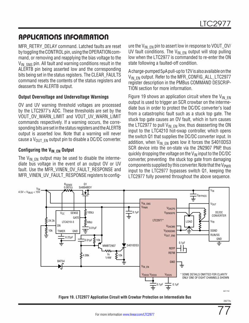
LTC2977
772977fc
For more information www.linear.com/LTC2977
APPLICATIONS INFORMATIONMFR_RETRY_DELAY command. Latched faults are reset by toggling the CONTROL pin, using the OPERATION com-mand, or removing and reapplying the bias voltage to the VIN_SNS pin. All fault and warning conditions result in the ALERTB pin being asserted low and the corresponding bits being set in the status registers. The CLEAR_FAULTS command resets the contents of the status registers and deasserts the ALERTB output.
Output Overvoltage and Undervoltage Warnings
OV and UV warning threshold voltages are processed by the LTC2977’s ADC. These thresholds are set by the VOUT_OV_WARN_LIMIT and VOUT_UV_WARN_LIMIT commands respectively. If a warning occurs, the corre-sponding bits are set in the status registers and the ALERTB output is asserted low. Note that a warning will never cause a VOUT_EN output pin to disable a DC/DC converter.
Configuring the VIN_EN Output
The VIN_EN output may be used to disable the interme-diate bus voltage in the event of an output OV or UV fault. Use the MFR_VINEN_OV_FAULT_RESPONSE and MFR_VINEN_UV_FAULT_RESPONSE registers to config-
ure the VIN_EN pin to assert low in response to VOUT_OV/UV fault conditions. The VIN_EN output will stop pulling low when the LTC2977 is commanded to re-enter the ON state following a faulted-off condition.
A charge-pumped 5µA pull-up to 12V is also available on the VIN_EN output. Refer to the MFR_CONFIG_ALL_LTC2977 register description in the PMBus COMMAND DESCRIP-TION section for more information.
Figure 19 shows an application circuit where the VIN_EN output is used to trigger an SCR crowbar on the interme-diate bus in order to protect the DC/DC converter’s load from a catastrophic fault such as a stuck top gate. The stuck top gate causes an OV fault, which in turn causes the LTC2977 to pull VIN_EN low, thus deasserting the ON input to the LTC4210 hot-swap controller, which opens the switch Q1 that supplies the DC/DC converter input. In addition, when VIN_EN goes low it forces the S4010DS3 SCR device into the on-state via the 2N2907 PNP, thus quickly dropping the voltage on the VIN input to the DC/DC converter, preventing the stuck top gate from damaging components supplied by this converter. Note that the VPWR input to the LTC2977 bypasses switch Q1, keeping the LTC2977 fully powered throughout the above sequence.
Figure 19. LTC2977 Application Circuit with Crowbar Protection on Intermediate Bus
VPWR
VIN_SNS
VIN_EN
VDACP0
VSENSEP0
VDACM0
VSENSEM0
VOUT_EN0
REFP
REFM
GND
LTC2977*
VIN4.5V < VIBUS < 15V
VDD33 VDD33 VDD25 * SOME DETAILS OMITTED FOR CLARITY ONLY ONE OF EIGHT CHANNELS SHOWN
VIN
CBYPASS
0.1µF
0.01µF0.22µF
0.01µF
0.1µF
10k
S4010DS3
0.1µF 0.1µF
VOUT
2977 F19
RUN/SSSGND
VFB
GND
DC/DCCONVERTER
LOAD
4.99k
BAT54
10k
100Ω
68Ω
VCC SENSE
RSENSE0.007Ω
Q1Si4894BDY
LTC4210-3
TIMER GND
GATE24.3k
10k
ON
MMBT2907
1k1/4W
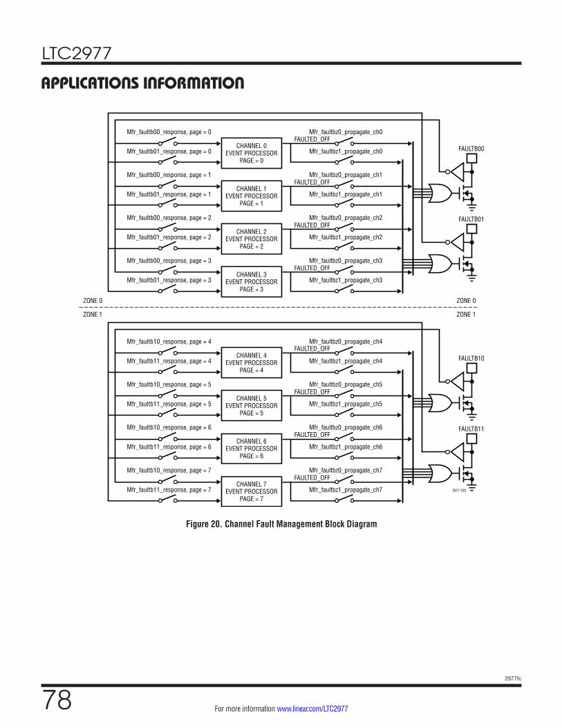
LTC2977
782977fc
For more information www.linear.com/LTC2977
APPLICATIONS INFORMATION
Figure 20. Channel Fault Management Block Diagram
CHANNEL 0EVENT PROCESSOR
PAGE = 0
Mfr_faultb00_response, page = 0
Mfr_faultb01_response, page = 0
Mfr_faultbz0_propagate_ch0
FAULTB00Mfr_faultbz1_propagate_ch0
CHANNEL 1EVENT PROCESSOR
PAGE = 1
Mfr_faultb00_response, page = 1
Mfr_faultb01_response, page = 1
Mfr_faultbz0_propagate_ch1
Mfr_faultbz1_propagate_ch1
CHANNEL 2EVENT PROCESSOR
PAGE = 2
Mfr_faultb00_response, page = 2
Mfr_faultb01_response, page = 2
Mfr_faultbz0_propagate_ch2
Mfr_faultbz1_propagate_ch2
CHANNEL 3EVENT PROCESSOR
PAGE = 3
ZONE 0
ZONE 1
ZONE 0
ZONE 1
Mfr_faultb00_response, page = 3
Mfr_faultb01_response, page = 3
Mfr_faultbz0_propagate_ch3
Mfr_faultbz1_propagate_ch3
FAULTB01
CHANNEL 4EVENT PROCESSOR
PAGE = 4
Mfr_faultb10_response, page = 4
Mfr_faultb11_response, page = 4
Mfr_faultbz0_propagate_ch4
FAULTB10Mfr_faultbz1_propagate_ch4
CHANNEL 5EVENT PROCESSOR
PAGE = 5
Mfr_faultb10_response, page = 5
Mfr_faultb11_response, page = 5
Mfr_faultbz0_propagate_ch5
Mfr_faultbz1_propagate_ch5
CHANNEL 6EVENT PROCESSOR
PAGE = 6
Mfr_faultb10_response, page = 6
Mfr_faultb11_response, page = 6
Mfr_faultbz0_propagate_ch6
Mfr_faultbz1_propagate_ch6
CHANNEL 7EVENT PROCESSOR
PAGE = 7
Mfr_faultb10_response, page = 7
Mfr_faultb11_response, page = 7
Mfr_faultbz0_propagate_ch7
Mfr_faultbz1_propagate_ch7
FAULTED_OFF
FAULTED_OFF
FAULTED_OFF
FAULTED_OFF
FAULTED_OFF
FAULTED_OFF
FAULTED_OFF
FAULTED_OFF
FAULTB11
2977 F20
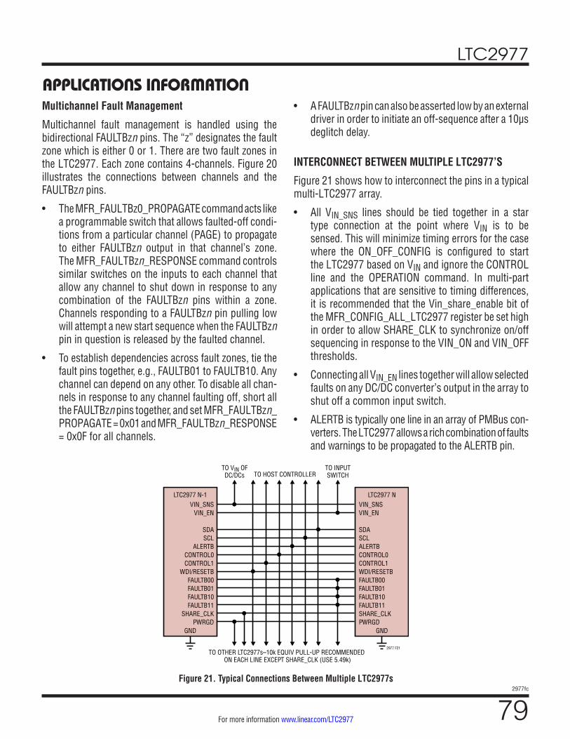
LTC2977
792977fc
For more information www.linear.com/LTC2977
APPLICATIONS INFORMATIONMultichannel Fault Management
Multichannel fault management is handled using the bidirectional FAULTBzn pins. The “z” designates the fault zone which is either 0 or 1. There are two fault zones in the LTC2977. Each zone contains 4-channels. Figure 20 illustrates the connections between channels and the FAULTBzn pins.
• The MFR_FAULTBz0_PROPAGATE command acts like a programmable switch that allows faulted-off condi-tions from a particular channel (PAGE) to propagate to either FAULTBzn output in that channel’s zone. The MFR_FAULTBzn_RESPONSE command controls similar switches on the inputs to each channel that allow any channel to shut down in response to any combination of the FAULTBzn pins within a zone. Channels responding to a FAULTBzn pin pulling low will attempt a new start sequence when the FAULTBzn pin in question is released by the faulted channel.
• To establish dependencies across fault zones, tie the fault pins together, e.g., FAULTB01 to FAULTB10. Any channel can depend on any other. To disable all chan-nels in response to any channel faulting off, short all the FAULTBzn pins together, and set MFR_FAULTBzn_PROPAGATE = 0x01 and MFR_FAULTBzn_RESPONSE = 0x0F for all channels.
• A FAULTBzn pin can also be asserted low by an external driver in order to initiate an off-sequence after a 10µs deglitch delay.
INTERCONNECT BETWEEN MULTIPLE LTC2977’S
Figure 21 shows how to interconnect the pins in a typical multi-LTC2977 array.
• All VIN_SNS lines should be tied together in a star type connection at the point where VIN is to be sensed. This will minimize timing errors for the case where the ON_OFF_CONFIG is configured to start the LTC2977 based on VIN and ignore the CONTROL line and the OPERATION command. In multi-part applications that are sensitive to timing differences, it is recommended that the Vin_share_enable bit of the MFR_CONFIG_ALL_LTC2977 register be set high in order to allow SHARE_CLK to synchronize on/off sequencing in response to the VIN_ON and VIN_OFF thresholds.
• Connecting all VIN_EN lines together will allow selected faults on any DC/DC converter’s output in the array to shut off a common input switch.
• ALERTB is typically one line in an array of PMBus con-verters. The LTC2977 allows a rich combination of faults and warnings to be propagated to the ALERTB pin.
Figure 21. Typical Connections Between Multiple LTC2977s
VIN_SNSVIN_EN
SDASCL
ALERTBCONTROL0CONTROL1
WDI/RESETBFAULTB00FAULTB01FAULTB10FAULTB11
SHARE_CLKPWRGD
GND
LTC2977 N-1VIN_SNSVIN_EN
SDASCLALERTBCONTROL0CONTROL1WDI/RESETBFAULTB00FAULTB01FAULTB10FAULTB11SHARE_CLKPWRGD
GND
2977 F21
LTC2977 N
TO VIN OFDC/DCs
TO INPUTSWITCHTO HOST CONTROLLER
TO OTHER LTC2977s–10k EQUIV PULL-UP RECOMMENDED ON EACH LINE EXCEPT SHARE_CLK (USE 5.49k)
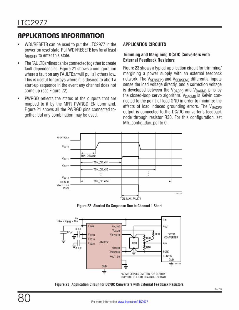
LTC2977
802977fc
For more information www.linear.com/LTC2977
APPLICATIONS INFORMATION• WDI/RESETB can be used to put the LTC2977 in the
power-on reset state. Pull WDI/RESETB low for at least tRESETB to enter this state.
• The FAULTBzn lines can be connected together to create fault dependencies. Figure 21 shows a configuration where a fault on any FAULTBzn will pull all others low. This is useful for arrays where it is desired to abort a start-up sequence in the event any channel does not come up (see Figure 22).
• PWRGD reflects the status of the outputs that are mapped to it by the MFR_PWRGD_EN command. Figure 21 shows all the PWRGD pins connected to-gether, but any combination may be used.
APPLICATION CIRCUITS
Trimming and Margining DC/DC Converters with External Feedback Resistors
Figure 23 shows a typical application circuit for trimming/margining a power supply with an external feedback network. The VSENSEP0 and VSENSEM0 differential inputs sense the load voltage directly, and a correction voltage is developed between the VDACP0 and VDACM0 pins by the closed-loop servo algorithm. VDACM0 is Kelvin con-nected to the point-of-load GND in order to minimize the effects of load induced grounding errors. The VDACP0 output is connected to the DC/DC converter’s feedback node through resistor R30. For this configuration, set Mfr_config_dac_pol to 0.
Figure 22. Aborted On Sequence Due to Channel 1 Short
VCONTROLn
VOUT0
TON_DELAY0VOUT1
VOUT2
VOUTn
BUSSEDVFAULTBzn
PINS
TON_MAX_FAULT1
2977 F22
TON_DELAY1
TON_DELAY2
TON_DELAYn
•••
•••
Figure 23. Application Circuit for DC/DC Converters with External Feedback Resistors
VPWR
VDD33
VDD33
VDD25
VIN_SNS
VDACP0
VSENSEP0
VDACM0
VSENSEM0
VOUT_EN0
LTC2977*
0.1µF
0.1µF
VIN4.5V < VIBUS < 15V
GND
*SOME DETAILS OMITTED FOR CLARITYONLY ONE OF EIGHT CHANNELS SHOWN
VIN
VOUT
R20R30
R10
2977 F23
RUN/SSSGND
VFB
GND
DC/DCCONVERTER
LOAD
0.1µF

LTC2977
812977fc
For more information www.linear.com/LTC2977
APPLICATIONS INFORMATIONFour-Step Resistor Selection Procedure for DC/DC Converters with External Feedback Resistors
The following four-step procedure should be used to calculate the resistor values required for the application circuit shown in Figure 23.
1. Assume values for feedback resistor R20 and the nominal DC/DC converter output voltage VDC(NOM), and solve for R10.
VDC(NOM) is the output voltage of the DC/DC converter when the LTC2977’s VDACP0 pin is in a high impedance state. R10 is a function of R20, VDC(NOM), the voltage at the feedback node (VFB) when the loop is in regulation, and the feedback node’s input current (IFB).
R10 = R20 • VFB
VDC(NOM) – IFB • R20 – VFB (1)
2. Solve for the value of R30 that yields the maximum required DC/DC converter output voltage VDC(MAX).
When VDACP0 is at 0V, the output of the DC/DC converter is at its maximum voltage.
R30 ≤ R20 • VFB
VDC(MAX) – VDC(NOM) (2)
3. Solve for the minimum value of VDACP0 that is needed to yield the minimum required DC/DC converter output voltage VDC(MIN).
The DAC has two full-scale settings, 1.38V and 2.65V. In order to select the appropriate full-scale setting, cal-culate the minimum required VFS_VDAC output voltage:
VFS _VDAC> VDC(NOM) – VDC(MIN)( ) • R30
R20+VFB (3)
4. Recalculate the minimum, nominal, and maximum DC/DC converter output voltages and the resulting margin-ing resolution.
VDC(NOM) = VFB • 1+ R20R10
+IFB •R20 (4)
VDC(MIN) = VDC(NOM) – R20R30
• VFS_VDAC – VFB( ) (5)
VDC(MAX) = VDC(NOM) + R20R30
• VFB (6)
VRES =
R20R30
• VFS_VDAC
1023V/DAC LSB (7)
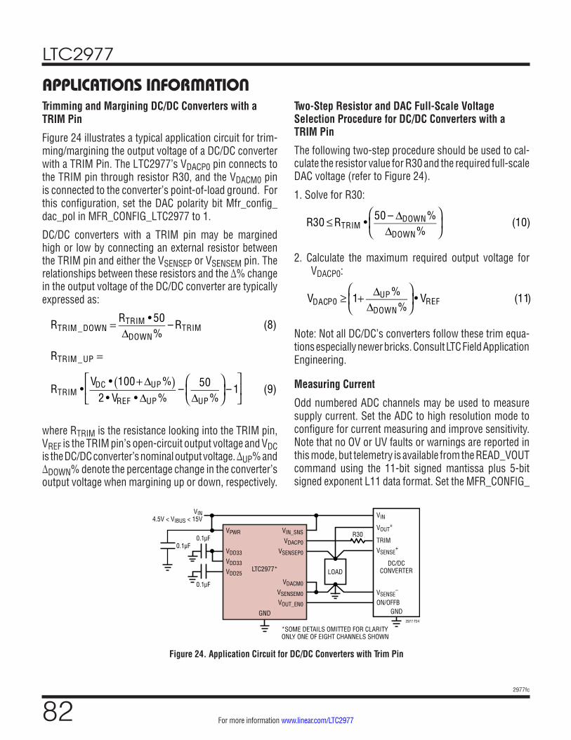
LTC2977
822977fc
For more information www.linear.com/LTC2977
APPLICATIONS INFORMATIONTrimming and Margining DC/DC Converters with a TRIM Pin
Figure 24 illustrates a typical application circuit for trim-ming/margining the output voltage of a DC/DC converter with a TRIM Pin. The LTC2977’s VDACP0 pin connects to the TRIM pin through resistor R30, and the VDACM0 pin is connected to the converter’s point-of-load ground. For this configuration, set the DAC polarity bit Mfr_config_ dac_pol in MFR_CONFIG_LTC2977 to 1.
DC/DC converters with a TRIM pin may be margined high or low by connecting an external resistor between the TRIM pin and either the VSENSEP or VSENSEM pin. The relationships between these resistors and the ∆% change in the output voltage of the DC/DC converter are typically expressed as:
RTRIM _DOWN = RTRIM • 50∆DOWN%
– RTRIM (8)
RTRIM _UP =
RTRIM •VDC • 100+ ∆UP %( )
2 • VREF • ∆UP %– 50
∆UP %
– 1
(9)
where RTRIM is the resistance looking into the TRIM pin, VREF is the TRIM pin’s open-circuit output voltage and VDC is the DC/DC converter’s nominal output voltage. ∆UP% and ∆DOWN% denote the percentage change in the converter’s output voltage when margining up or down, respectively.
Two-Step Resistor and DAC Full-Scale Voltage Selection Procedure for DC/DC Converters with a TRIM Pin
The following two-step procedure should be used to cal-culate the resistor value for R30 and the required full-scale DAC voltage (refer to Figure 24).
1. Solve for R30:
R30 ≤ RTRIM • 50 – ∆DOWN%
∆DOWN%
(10)
2. Calculate the maximum required output voltage for VDACP0:
VDACP0 ≥ 1+ ∆UP %
∆DOWN%
• VREF (11)
Note: Not all DC/DC’s converters follow these trim equa-tions especially newer bricks. Consult LTC Field Application Engineering.
Measuring Current
Odd numbered ADC channels may be used to measure supply current. Set the ADC to high resolution mode to configure for current measuring and improve sensitivity. Note that no OV or UV faults or warnings are reported in this mode, but telemetry is available from the READ_VOUT command using the 11-bit signed mantissa plus 5-bit signed exponent L11 data format. Set the MFR_CONFIG_
Figure 24. Application Circuit for DC/DC Converters with Trim Pin
VPWR
VDD33
VDD33
VDD25
VIN_SNS
VDACP0
VSENSEP0
VDACM0
VSENSEM0
VOUT_EN0
LTC2977*
0.1µF
0.1µF
VIN4.5V < VIBUS < 15V
GND
*SOME DETAILS OMITTED FOR CLARITYONLY ONE OF EIGHT CHANNELS SHOWN
VIN
VOUT+
TRIM
2977 F24
ON/OFFBVSENSE
–
VSENSE+
GND
DC/DCCONVERTERLOAD
R30
0.1µF
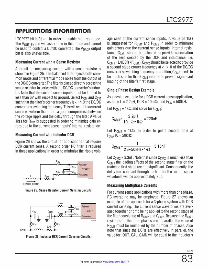
LTC2977
832977fc
For more information www.linear.com/LTC2977
APPLICATIONS INFORMATIONLTC2977 bit b[9] = 1 in order to enable high res mode. The VOUT_EN pin will assert low in this mode and cannot be used to control a DC/DC converter. The VDACP output pin is also unavailable.
Measuring Current with a Sense Resistor
A circuit for measuring current with a sense resistor is shown in Figure 25. The balanced filter rejects both com-mon mode and differential mode noise from the output of the DC/DC converter. The filter is placed directly across the sense resistor in series with the DC/DC converter’s induc-tor. Note that the current sense inputs must be limited to less than 6V with respect to ground. Select RCM and CCM such that the filter’s corner frequency is < 1/10 the DC/DC converter’s switching frequency. This will result in a current sense waveform that offers a good compromise between the voltage ripple and the delay through the filter. A value 1kΩ for RCM is suggested in order to minimize gain er-rors due to the current sense inputs’ internal resistance.
Measuring Current with Inductor DCR
Figure 26 shows the circuit for applications that require DCR current sense. A second order RC filter is required in these applications in order to minimize the ripple volt-
age seen at the current sense inputs. A value of 1kΩ is suggested for RCM1 and RCM2 in order to minimize gain errors due the current sense inputs’ internal resis-tance. CCM1 should be selected to provide cancellation of the zero created by the DCR and inductance, i.e. CCM1 = L/(DCR • RCM1). CCM2 should be selected to provide a second stage corner frequency at < 1/10 of the DC/DC converter’s switching frequency. In addition, CCM2 needs to be much smaller than CCM1 in order to prevent significant loading of the filter’s first stage.
Single Phase Design Example
As a design example for a DCR current sense application, assume L = 2.2μH, DCR = 10mΩ, and FSW = 500kHz.
Let RCM1 = 1kΩ and solve for CCM1:
CCM1≥
2.2µH10mΩ • 1kΩ
= 220nF
Let RCM2 = 1kΩ. In order to get a second pole at FSW/10 = 50kHz:
CCM2 =
12 ≠•50kHz • 1kΩ
= 3.18nF
Let CCM2 = 3.3nF. Note that since CCM2 is much less than CCM1 the loading effects of the second stage filter on the matched first stage are not significant. Consequently, the delay time constant through the filter for the current sense waveform will be approximately 3μs.
Measuring Multiphase Currents
For current sense applications with more than one phase, RC averaging may be employed. Figure 27 shows an example of this approach for a 3-phase system with DCR current sensing. The current sense waveforms are aver-aged together prior to being applied to the second stage of the filter consisting of RCM2 and CCM2. Because the RCM1 resistors for the three phases are in parallel, the value of RCM1 must be multiplied by the number of phases. Also note that since the DCRs are effectively in parallel, the value for IOUT_CAL_GAIN will be equal to the inductor’s
Figure 25. Sense Resistor Current Sensing Circuits
RCM
RCM
RSNS2977 F25
L
LOAD CURRENT
CCM
CCMLTC2977
VSENSEP1
VSENSEM1
Figure 26. Inductor DCR Current Sensing Circuits
RCM2
RCM2
RCM1RCM1DCR
2977 F26
LSWX0
CCM2CCM1CCM1
CCM2LTC2977
VSENSEP1
VSENSEM1

LTC2977
842977fc
For more information www.linear.com/LTC2977
APPLICATIONS INFORMATION
DCR divided by the number of phases. Care should to be taken in the layout of the multiphase inductors to keep the PCB trace resistance from the DC side of each inductor to the summing node balanced in order to provide the most accurate results.
Multiphase Design Example
Using the same values for inductance and DCR from the previous design example, the value for RCM1 will be 3kΩ for a three phase DC/DC converter if CCM1 is left at 220nF. Similarly, the value for IOUT_CAL_GAIN will be DCR/3 = 3.33mΩ.
Anti-aliasing Filter Considerations
Noisy environments require an anti-aliasing filter on the input to the LTC2977’s ADC. The R-C circuit shown in Figure 28 is adequate for most situations. Keep R40 = R50 ≤ 200Ω to minimize ADC gain errors, and select a value for capacitors C10 and C20 that does not add too much additional response time to the OV/UV supervisor, e.g. τ ≅ 10µs (R = 100Ω, C = 0.10µF).
Figure 28. Anti-Aliasing Filter on VSENSE Lines
VPWR
VDD33
VDD33
VDD25
VIN_SNS
VDACP0
VSENSEP0
VSENSEM0
VDACM0
VOUT_EN0
LTC2977*
0.1µF
0.1µF
VIN4.5V < VIBUS < 15V
GND *SOME DETAILS OMITTED FOR CLARITYONLY ONE OF EIGHT CHANNELS SHOWN
VIN
VOUT
R20R30
R10
2977 F28
RUN/SSSGND
VFB
GND
DC/DCCONVERTER
LOAD
C10
C20 R50
R40
0.1µF
Figure 27. Multiphase DCR Current Sensing Circuits
RCM2RCM1
RCM1
RCM1
RCM2RCM1/3
DCR
DCRDCR
L
LL
2977 F27
TO LOAD
SWX3SWX2
SWX1
LTC2977
VSENSEP1
VSENSEM1
CCM2CCM1
CCM1 CCM2
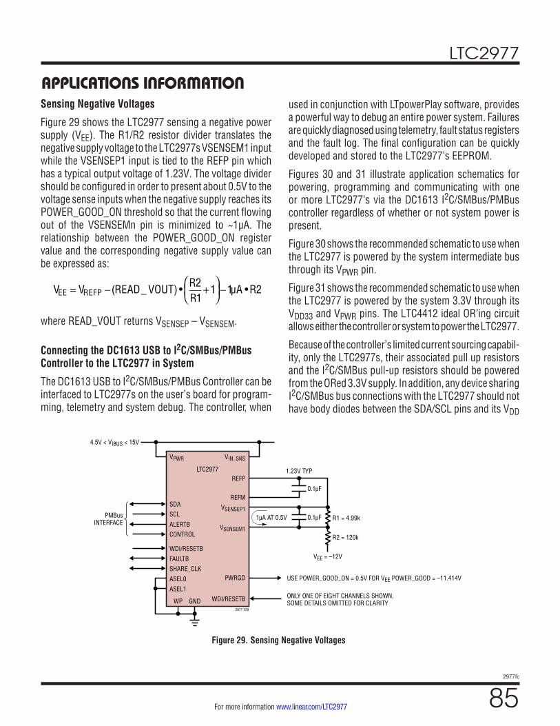
LTC2977
852977fc
For more information www.linear.com/LTC2977
Sensing Negative Voltages
Figure 29 shows the LTC2977 sensing a negative power supply (VEE). The R1/R2 resistor divider translates the negative supply voltage to the LTC2977s VSENSEM1 input while the VSENSEP1 input is tied to the REFP pin which has a typical output voltage of 1.23V. The voltage divider should be configured in order to present about 0.5V to the voltage sense inputs when the negative supply reaches its POWER_GOOD_ON threshold so that the current flowing out of the VSENSEMn pin is minimized to ~1µA. The relationship between the POWER_GOOD_ON register value and the corresponding negative supply value can be expressed as:
VEE = VREFP −(READ_ VOUT) • R2
R1+1
−1µA •R2
where READ_VOUT returns VSENSEP – VSENSEM.
Connecting the DC1613 USB to I2C/SMBus/PMBus Controller to the LTC2977 in System
The DC1613 USB to I2C/SMBus/PMBus Controller can be interfaced to LTC2977s on the user’s board for program-ming, telemetry and system debug. The controller, when
used in conjunction with LTpowerPlay software, provides a powerful way to debug an entire power system. Failures are quickly diagnosed using telemetry, fault status registers and the fault log. The final configuration can be quickly developed and stored to the LTC2977’s EEPROM.
Figures 30 and 31 illustrate application schematics for powering, programming and communicating with one or more LTC2977’s via the DC1613 I2C/SMBus/PMBus controller regardless of whether or not system power is present.
Figure 30 shows the recommended schematic to use when the LTC2977 is powered by the system intermediate bus through its VPWR pin.
Figure 31 shows the recommended schematic to use when the LTC2977 is powered by the system 3.3V through its VDD33 and VPWR pins. The LTC4412 ideal OR’ing circuit allows either the controller or system to power the LTC2977.
Because of the controller’s limited current sourcing capabil-ity, only the LTC2977s, their associated pull up resistors and the I2C/SMBus pull-up resistors should be powered from the ORed 3.3V supply. In addition, any device sharing I2C/SMBus bus connections with the LTC2977 should not have body diodes between the SDA/SCL pins and its VDD
APPLICATIONS INFORMATION
Figure 29. Sensing Negative Voltages
LTC2977
4.5V < VIBUS < 15V
GNDONLY ONE OF EIGHT CHANNELS SHOWN,SOME DETAILS OMITTED FOR CLARITY
USE POWER_GOOD_ON = 0.5V FOR VEE POWER_GOOD = –11.414V
0.1µF
1.23V TYP
2977 F29
VPWR
SDA
SCL
ALERTB
CONTROL
FAULTB
WDI/RESETB
SHARE_CLK
ASEL0
ASEL1
WP
VIN_SNS
REFM
VSENSEP1
WDI/RESETB
VSENSEM1
REFP
PWRGD
0.1µF R1 = 4.99k1µA AT 0.5V
R2 = 120k
VEE = –12V
PMBusINTERFACE
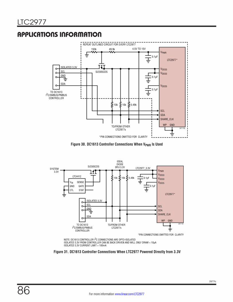
LTC2977
862977fc
For more information www.linear.com/LTC2977
APPLICATIONS INFORMATION
Figure 31. DC1613 Controller Connections When LTC2977 Powered Directly from 3.3V
VPWR
VDD33
VDD33
VDD25
SCL
SDA
SHARE_CLK
LTC2977_3.3V
IDEALDIODE
0R’d 3.3V
0.1µF
0.1µF
WP GND2977 F31
5.49k
LTC2977*
TO DC1613I2C/SMBUS/PMBUS
CONTROLLER
NOTE: DC1613 CONTROLLER I2C CONNECTIONS ARE OPTO-ISOLATEDISOLATED 3.3V FROM CONTROLLER CAN BE BACK DRIVEN AND WILL ONLY DRAW < 10µAISOLATED 3.3V CURRENT LIMIT = 100mA
TO/FROM OTHERLTC2977s
10k10k
SYSTEM3.3V
Si2305CDS
VIN
GND
CTL
SENSE
GATE
STAT
LTC4412
ISOLATED 3.3V
SCL
SDA
GND
*PIN CONNECTIONS OMITTED FOR CLARITY
Figure 30. DC1613 Controller Connections When VPWR Is Used
VPWR
VDD33
VDD33
VDD25
SCL
SDA
SHARE_CLK
LTC2977*0.1µF
4.5V TO 15V
0.1µF
0.1µF
WP GND2977 F30
5.49k10k
49.9k
Si2305CDS
TO DC1613I2C/SMBUS/PMBUS
CONTROLLER
TO/FROM OTHERLTC2977s
150k
REPEAT OUTLINED CIRCUIT FOR EVERY LTC2977
10k
ISOLATED 3.3V
SCL
SDA
GND
*PIN CONNECTIONS OMITTED FOR CLARITY
LTC2977
872977fc
For more information www.linear.com/LTC2977
APPLICATIONS INFORMATIONnode because this will interfere with bus communication in the absence of system power.
The DC1613 controller’s I2C/SMBus connections are opto-isolated from the PC’s USB port. The 3.3V supply from the controller and the LTC2977’s VDD33 pin can be paralleled because the LTC LDOs that generate these volt-ages can be backdriven and draw <10μA. The controller’s 3.3V current limit is 100mA.
DESIGN CHECKLIST
I2C n The LTC2977 must be configured for a unique ad-
dress. n The address select pins (ASELn) are tri-level; check
Table 1. n Check addresses for collision with other devices on
the bus and any global addresses.
Output Enables n Use appropriate pull-up resistors on all VOUT_ENn
pins. n Verify that the absolute maximum ratings of the
VOUT_ENn pins are not exceeded.
VIN Sense n No external resistive divider is required to sense VIN;
VIN_SNS already has an internal calibrated divider.
Logic Signals n Verify the absolute maximum ratings of the digital
pins (SCL, SDA, ALERTB, FAULTBzn, CONTROLn, SHARE_CLK, WDI, ASELn, PWRGD) are not ex-ceeded.
n Short all SHARE_CLK pins in the system together and pull up to 3.3V with a 5.49k resistor.
n Do not leave CONTROLn pins floating. Pull up to 3.3V with a 10k resistor.
n Tie WDI/RESETB to VDD33 with a 10k resistor. Do not connect a capacitor to the WDI/RESETB pin.
n Tie WP to either VDD33 or GND. Do not leave floating.
Unused Inputsn Connect all unused VSENSEPn, VSENSEMn and DACMn
pins to GND. Do not float unused inputs. Refer to Un-used ADC Sense Inputs in the Applications Information section.
DAC Outputs n Select appropriate resistor for desired margin range.
Refer to the resistor selection tool in LTpowerPlay for assistance.
For a more complete list of design considerations and a schematic checklist, see the Design Checklist on the LTC2977 product page:
www.linear.com/LTC2977
LTpowerPlay: AN INTERACTIVE GUI FOR POWER SYSTEM MANAGERS
LTpowerPlay is a powerful Windows based develop-ment environment that supports Linear Technology Power System Manager ICs with EEPROM, including the LTC2977 8-channel PMBus Power System Manager. The software supports a variety of different tasks. You can use LTpowerPlay to evaluate Linear Technology ICs by connecting to a demo board system. LTpowerPlay can also be used in an offline mode (with no hardware pres-ent) in order to build a multi-chip configuration file that can be saved and reloaded at a later time. LTpowerPlay provides unprecedented diagnostic and debug features. It becomes a valuable diagnostic tool during board bring-up to program or tweak the power management scheme in a system or to diagnose power issues when bringing up rails. LTpowerPlay utilizes Linear Technology’s DC1613 USB-to-I2C/SMBus/PMBus Controller to communicate with one of many potential targets, including the DC2028 demo board set, the DC1508 socketed programming board, or a customer target system. The software also provides an automatic update feature to keep the software current with the latest set of device drivers and documentation. A great deal of context sensitive help is available within LTpowerPlay along with several tutorial demos. Complete information is available at:
www.linear.com/ltpowerplay
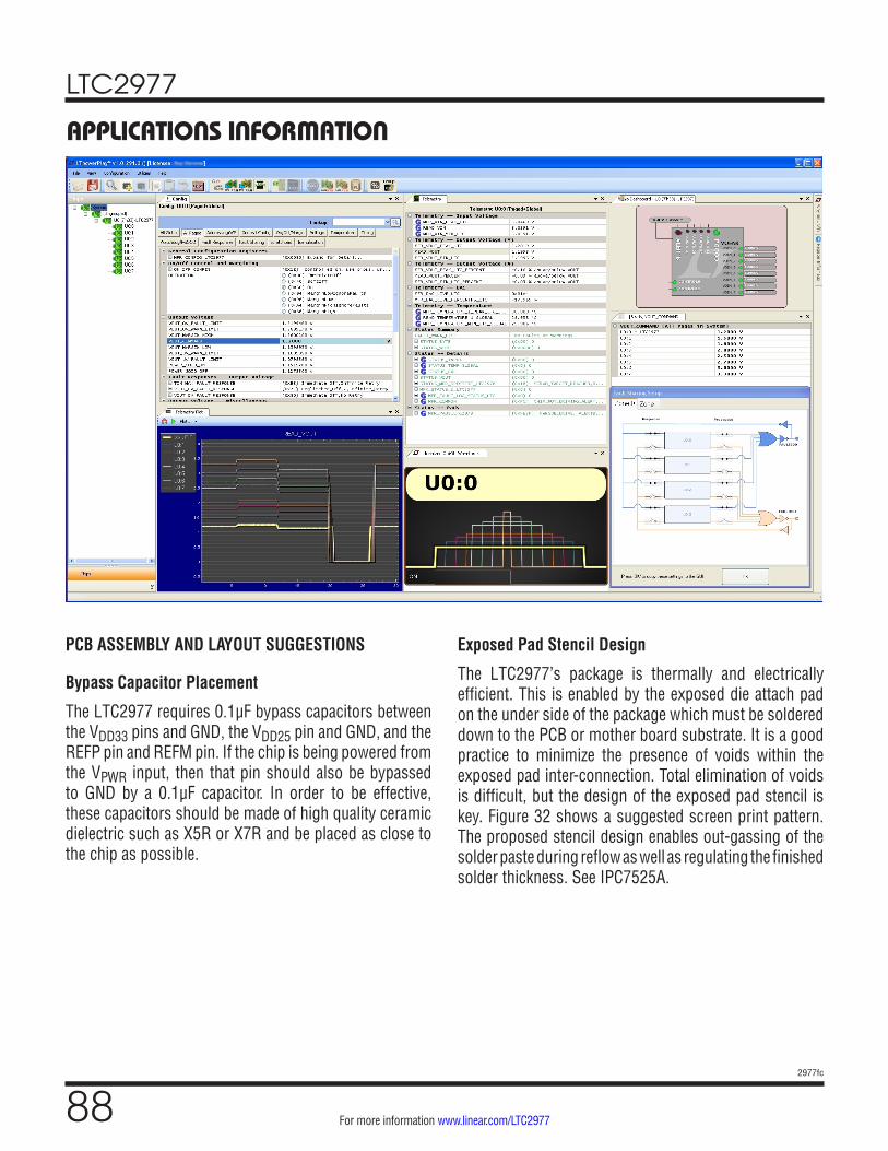
LTC2977
882977fc
For more information www.linear.com/LTC2977
APPLICATIONS INFORMATION
PCB ASSEMBLY AND LAYOUT SUGGESTIONS
Bypass Capacitor Placement
The LTC2977 requires 0.1µF bypass capacitors between the VDD33 pins and GND, the VDD25 pin and GND, and the REFP pin and REFM pin. If the chip is being powered from the VPWR input, then that pin should also be bypassed to GND by a 0.1µF capacitor. In order to be effective, these capacitors should be made of high quality ceramic dielectric such as X5R or X7R and be placed as close to the chip as possible.
Exposed Pad Stencil Design
The LTC2977’s package is thermally and electrically efficient. This is enabled by the exposed die attach pad on the under side of the package which must be soldered down to the PCB or mother board substrate. It is a good practice to minimize the presence of voids within the exposed pad inter-connection. Total elimination of voids is difficult, but the design of the exposed pad stencil is key. Figure 32 shows a suggested screen print pattern. The proposed stencil design enables out-gassing of the solder paste during reflow as well as regulating the finished solder thickness. See IPC7525A.
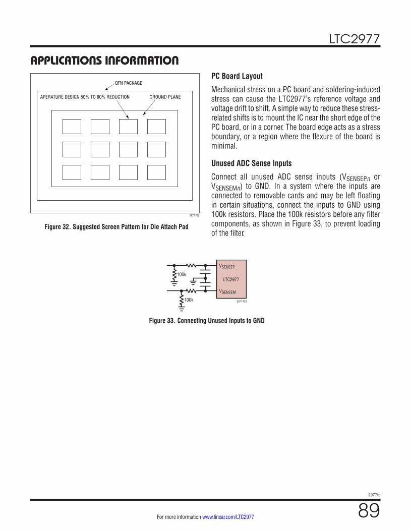
LTC2977
892977fc
For more information www.linear.com/LTC2977
APPLICATIONS INFORMATION
Figure 32. Suggested Screen Pattern for Die Attach Pad
Figure 33. Connecting Unused Inputs to GND
2977 F32
QFN PACKAGE
APERATURE DESIGN 50% TO 80% REDUCTION GROUND PLANE
100k
100k
VSENSEP
VSENSEM
LTC2977
2977 F33
PC Board Layout
Mechanical stress on a PC board and soldering-induced stress can cause the LTC2977’s reference voltage and voltage drift to shift. A simple way to reduce these stress-related shifts is to mount the IC near the short edge of the PC board, or in a corner. The board edge acts as a stress boundary, or a region where the flexure of the board is minimal.
Unused ADC Sense Inputs
Connect all unused ADC sense inputs (VSENSEPn or VSENSEMn) to GND. In a system where the inputs are connected to removable cards and may be left floating in certain situations, connect the inputs to GND using 100k resistors. Place the 100k resistors before any filter components, as shown in Figure 33, to prevent loading of the filter.
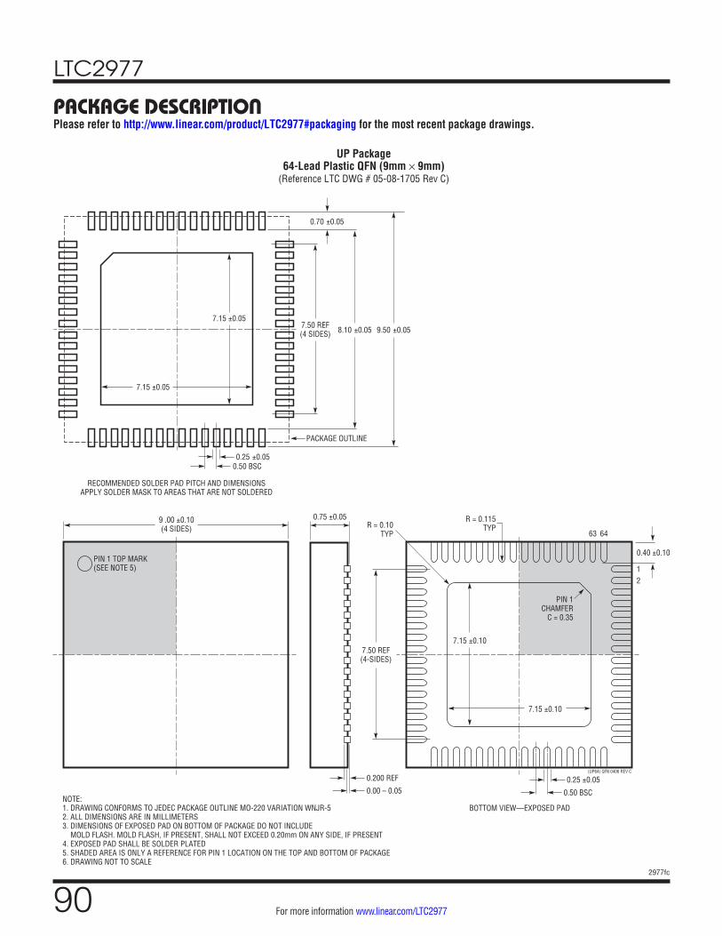
LTC2977
902977fc
For more information www.linear.com/LTC2977
PACKAGE DESCRIPTION
9 .00 ±0.10(4 SIDES)
NOTE:1. DRAWING CONFORMS TO JEDEC PACKAGE OUTLINE MO-220 VARIATION WNJR-52. ALL DIMENSIONS ARE IN MILLIMETERS3. DIMENSIONS OF EXPOSED PAD ON BOTTOM OF PACKAGE DO NOT INCLUDE MOLD FLASH. MOLD FLASH, IF PRESENT, SHALL NOT EXCEED 0.20mm ON ANY SIDE, IF PRESENT4. EXPOSED PAD SHALL BE SOLDER PLATED5. SHADED AREA IS ONLY A REFERENCE FOR PIN 1 LOCATION ON THE TOP AND BOTTOM OF PACKAGE 6. DRAWING NOT TO SCALE
PIN 1 TOP MARK(SEE NOTE 5)
0.40 ±0.10
6463
12
BOTTOM VIEW—EXPOSED PAD
7.15 ±0.10
7.15 ±0.10
7.50 REF(4-SIDES)
0.75 ±0.05R = 0.10
TYP
R = 0.115TYP
0.25 ±0.05
0.50 BSC
0.200 REF
0.00 – 0.05
(UP64) QFN 0406 REV C
RECOMMENDED SOLDER PAD PITCH AND DIMENSIONSAPPLY SOLDER MASK TO AREAS THAT ARE NOT SOLDERED
0.70 ±0.05
7.50 REF(4 SIDES)
7.15 ±0.05
7.15 ±0.05
8.10 ±0.05 9.50 ±0.05
0.25 ±0.050.50 BSC
PACKAGE OUTLINE
PIN 1CHAMFER
C = 0.35
UP Package64-Lead Plastic QFN (9mm × 9mm)
(Reference LTC DWG # 05-08-1705 Rev C)
Please refer to http://www.linear.com/product/LTC2977#packaging for the most recent package drawings.
LTC2977
912977fc
For more information www.linear.com/LTC2977
Information furnished by Linear Technology Corporation is believed to be accurate and reliable. However, no responsibility is assumed for its use. Linear Technology Corporation makes no representa-tion that the interconnection of its circuits as described herein will not infringe on existing patent rights.
REVISION HISTORYREV DATE DESCRIPTION PAGE NUMBER
A 09/13 Improved the voltage range for ADC Total Unadjusted Error (TUE) specification, Voltage Sense Mode, from >1.8V to >1V Added ADC TUE specification for Current Sense ModeConsolidated previous ADC specifications – INL, DNL, Voltage Sense Offset Error, Gain Error – into TUEUpdated VOS_CMP Offset Voltage specificationVVOUT_ENn Output High Voltage specification: Changed minimum from 11.6V to 10VAdded Typical Performance Characteristic: Closed-Loop Servo Accuracy
5
5577
11
B 08/16 Updated Typical Application and added EEPROM ECC informationUpdated DAC Output Update Rate (tS_VDACP)Added Note 3Updated graph: Closed Loop Servo ErrorAdded graph: VOUT_EN[7:0] Output Voltage vs VDD33
Updated VDD33, VDD25 and SHARE_CLK pin functionsUpdated value of k and resulting example in EEPROM sectionUpdated: Figures 1a, 7 to 12; Table 1Added MFR_INFO commandChanged MFR_SPECIAL_ID default valueAdded MFR_COMMAND_PLUS to list of excepted commands under Level 2 write protectionUpdated: WRITE_PROTECT Pin section, MFR_STATUS_PLUSn Data ContentsUpdated: STATUS_WORD b[0] operation, STATUS_VOUT b[3] symbol and operationUpdated description: MFR_VOUT_PEAK, MFR_VIN_PEAK, MFR_TEMPERATURE_PEAK, MFR_VOUT_MIN, MFR_VIN_MIN, MFR_TEMPERATURE_MINUpdated: Figure 19, P-channel MOSFETs in Figures 30 and 31Updated Design Checklist
1, 16, 17, 5869
11121317
19, 20, 2125, 5826, 58
2829, 3141, 42
56, 60, 61
79, 8687
C 04/17 Added VVOUT_VALID specifications 7
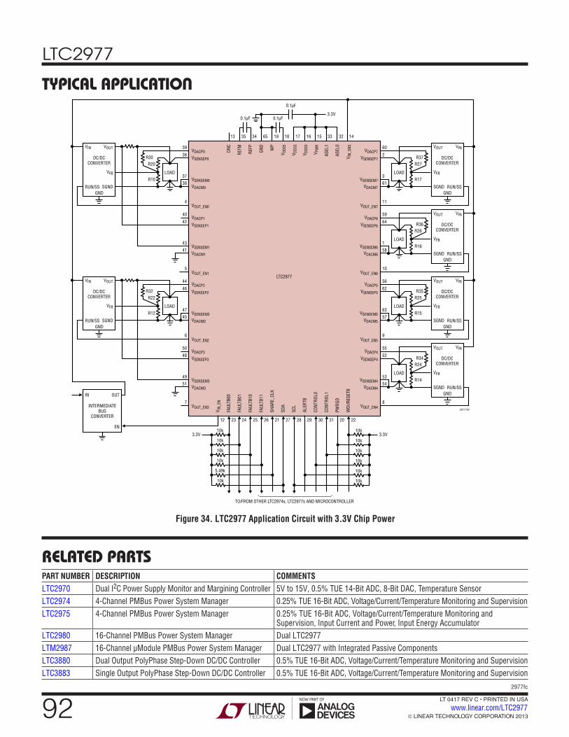
LTC2977
922977fc
For more information www.linear.com/LTC2977 LINEAR TECHNOLOGY CORPORATION 2013
LT 0417 REV C • PRINTED IN USAwww.linear.com/LTC2977
TYPICAL APPLICATION
Figure 34. LTC2977 Application Circuit with 3.3V Chip Power
VINVOUT
R27
61
11
60
2
338
4
39
36
37
R37R30
R17
R20
R10
RUN/SSSGND
VFB
GND
DC/DCCONVERTER
LOADLOAD
VDACP7
VSENSEP7
VSENSEM7
VDACM7
VOUT_EN7
VDACP0
VSENSEP0
VSENSEM0
VDACM0
VOUT_EN0
VINVOUT
R26
58
10
59
64
1
R36
R16
RUN/SSSGND
VFB
GND
DC/DCCONVERTER
LOAD
VDACP6
VSENSEP6
VSENSEM6
LTC2977
VDACM6
VOUT_EN6
VINVOUT
R25
57
9
56
62
63
R35
R15
RUN/SSSGND
VFB
GND
DC/DCCONVERTER
LOAD
VDACP5
VSENSEP5
VSENSEM5
VDACM5
VOUT_EN5
VINVOUT
R24
54
8
55
52
53
R34
R14
RUN/SSSGND
VFB
GND
2977 F34
DC/DCCONVERTER
LOAD
VDACP4
VSENSEP4
VSENSEM4
VDACM4
VOUT_EN4
VIN
RUN/SS
VOUT
SGND
VFB
GND
DC/DCCONVERTER
41
5
40
42
43
VDACP1
VSENSEP1
VSENSEM1
VDACM1
VOUT_EN1
45
6
44
46
47
R32R22
R12LOAD
VDACP2
VSENSEP2
VSENSEM2
VDACM2
VOUT_EN2
VIN
RUN/SS
VOUT
SGND
VFB
GND
DC/DCCONVERTER
IN OUT
EN
INTERMEDIATEBUS
CONVERTER
51
7
12
10k
50
48
49
VDACP3
VSENSEP3
VSENSEM3
VDACM3
VOUT_EN3
V IN_
EN
10k
10k
10k
5.49k
10k
10k
TO/FROM OTHER LTC2974s, LTC2977s AND MICROCONTROLLER
3.3V3.3V10k
10k
10k
10k
10k
23
FAUL
TB00
13
0.1µF
3435 65 19 18 17 16 15 33 32 14
3.3V
24
FAUL
TB01
25
FAUL
TB10
26
FAUL
TB11
21
SHAR
E_CL
K
27
SDA
28
SCL
29
ALER
TB
30
CONT
ROL0
31
CONT
ROL1
20
PWRG
D
22
WDI
/RES
ETB
DNC
REFM
REFP
GND
WP
V DD2
5
V DD3
3
V DD3
3
V PW
R
ASEL
1
ASEL
0
V IN_
SNS
0.1µF
0.1µF
RELATED PARTSPART NUMBER DESCRIPTION COMMENTSLTC2970 Dual I2C Power Supply Monitor and Margining Controller 5V to 15V, 0.5% TUE 14-Bit ADC, 8-Bit DAC, Temperature SensorLTC2974 4-Channel PMBus Power System Manager 0.25% TUE 16-Bit ADC, Voltage/Current/Temperature Monitoring and SupervisionLTC2975 4-Channel PMBus Power System Manager 0.25% TUE 16-Bit ADC, Voltage/Current/Temperature Monitoring and
Supervision, Input Current and Power, Input Energy AccumulatorLTC2980 16-Channel PMBus Power System Manager Dual LTC2977LTM2987 16-Channel µModule PMBus Power System Manager Dual LTC2977 with Integrated Passive ComponentsLTC3880 Dual Output PolyPhase Step-Down DC/DC Controller 0.5% TUE 16-Bit ADC, Voltage/Current/Temperature Monitoring and SupervisionLTC3883 Single Output PolyPhase Step-Down DC/DC Controller 0.5% TUE 16-Bit ADC, Voltage/Current/Temperature Monitoring and Supervision