ltc2107 – 16-bit, 210msps high performance adc · 2020-02-01 · defined radio and multi-channel...
TRANSCRIPT

LTC2107
12107fb
For more information www.linear.com/LTC2107
Block Diagram
Features Description
16-Bit, 210Msps High Performance ADC
The LTC®2107 is a 16-bit, 210Msps high performance ADC. The combination of high sample rate, low noise and high linearity enable a new generation of digital radio designs. The direct sampling front-end is designed specifically for the most demanding receiver applications such as software defined radio and multi-channel GSM base stations. The AC performance includes, SNR = 80dBFS, SFDR = 98dBFS. Aperture jitter = 45fsRMS allows direct sampling of IF frequencies up to 500MHz with excellent performance.
Features such as internal dither, a PGA front-end and digital output randomization help maximize performance. Modes of operation can be controlled through a 3-wire serial interface (SPI).
The double data rate (DDR) low voltage differential (LVDS) digital outputs help reduce digital line count and enable space saving designs.
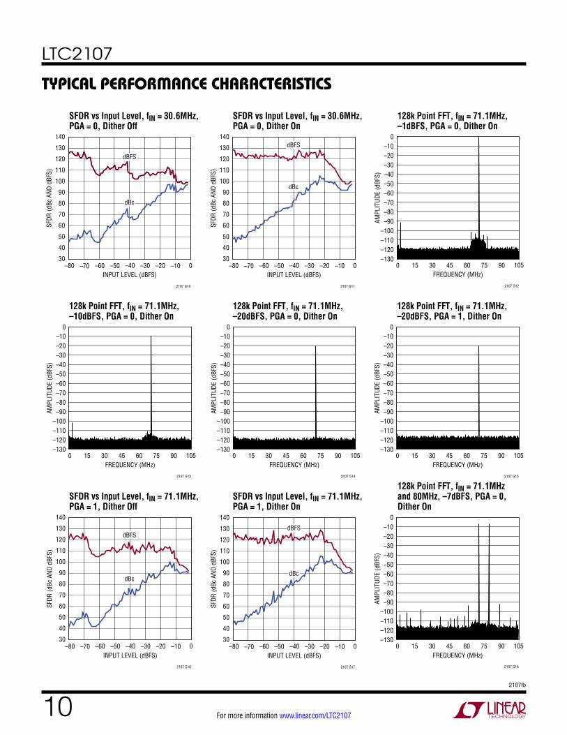
128k Point FFT, fIN = 30.6MHz, –1dBFS, PGA = 0
applications
n 98dBFS SFDRn 80dBFS SNR Noise Floorn Aperture Jitter = 45fsRMSn PGA Front-End 2.4VP-P or 1.6VP-P Input Rangen Optional Internal Dithern Optional Data Output Randomizern Power Dissipation: 1280mWn Shutdown Moden Serial SPI Port for Configurationn Clock Duty Cycle Stabilizern 48-Lead (7mm × 7mm) QFN Package
n Software Defined Radiosn Military Radio and RADARn Cellular Base Stationsn Spectral Analysisn Imaging Systemsn ATE and Instrumentation
–
+16-BIT
ADC COREINPUT
S/HANALOG
INPUTCORRECTION
LOGICOUTPUTBUFFERS
16CLKOUT±
OGND
2107 BD
D14_15±•••
D0_1±
1µF
10µF2.5V
1.8V
ENC+ ENC–
AIN–
AIN+
VCMVCM
SENSE
0V
GND
OF±
OVDD
CLOCK ANDCLOCK CONTROL
INTERNALREFERENCE
VCMDRIVER
SER/PAR SDI SCK CS SDO SHDN
ADC CONTROL/SPI INTERFACE
2.2µF
VDD
L, LT, LTC, LTM, Linear Technology and the Linear logo are registered trademarks of Linear Technology Corporation. All other trademarks are the property of their respective owners. Protected by U.S. Patents, including 7683695, 8482442, 8648741.
FREQUENCY (MHz)0 15 30 45 60 75 90
–140
AMPL
ITUD
E (d
BFS)
–120
–100
–80
0
–40
–20
–60
–130
–110
–90
–10
–50
–30
–70
105
2107 TA01
LTC2107
22107fb
For more information www.linear.com/LTC2107
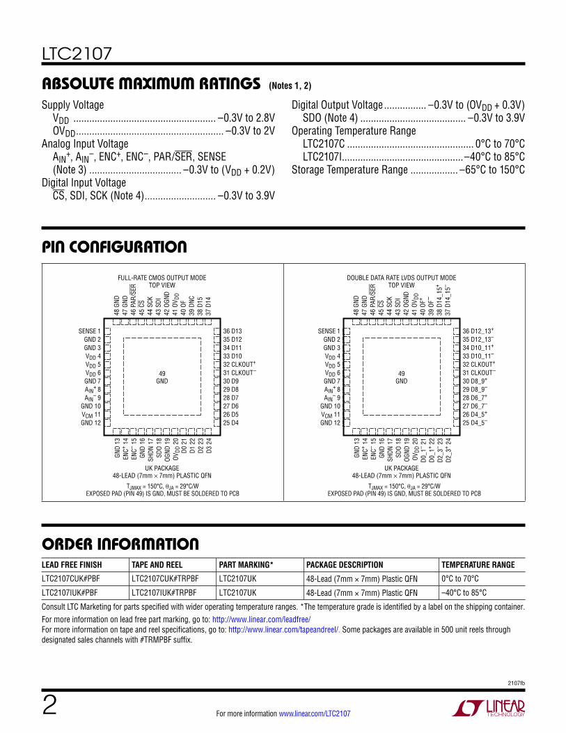
pin conFiguration
aBsolute maximum ratingsSupply Voltage VDD ...................................................... –0.3V to 2.8V OVDD ........................................................ –0.3V to 2VAnalog Input Voltage AIN
+, AIN–, ENC+, ENC–, PAR/SER, SENSE
(Note 3) ................................... –0.3V to (VDD + 0.2V)Digital Input Voltage CS, SDI, SCK (Note 4) ........................... –0.3V to 3.9V
(Notes 1, 2)
orDer inFormation
FULL-RATE CMOS OUTPUT MODETOP VIEW
49GND
UK PACKAGE48-LEAD (7mm × 7mm) PLASTIC QFN
SENSE 1GND 2GND 3VDD 4VDD 5VDD 6GND 7AIN
+ 8
AIN– 9
GND 10VCM 11GND 12
36 D1335 D1234 D1133 D1032 CLKOUT+
31 CLKOUT–
30 D929 D828 D727 D626 D525 D4
48 G
ND47
GND
46 P
AR/S
ER45
CS
44 S
CK43
SDI
42 O
GND
41 O
V DD
40 O
F39
DNC
38 D
1537
D14
GND
13EN
C+ 14
ENC– 1
5GN
D 16
SHDN
17
SDO
18OG
ND 1
9OV
DD 2
0 D
0 21
D1 2
2D2
23
D3 2
4
TJMAX = 150°C, θJA = 29°C/W
EXPOSED PAD (PIN 49) IS GND, MUST BE SOLDERED TO PCB
DOUBLE DATA RATE LVDS OUTPUT MODETOP VIEW
49GND
UK PACKAGE48-LEAD (7mm × 7mm) PLASTIC QFN
SENSE 1GND 2GND 3VDD 4VDD 5VDD 6GND 7AIN
+ 8
AIN– 9
GND 10VCM 11GND 12
36 D12_13+
35 D12_13–
34 D10_11+
33 D10_11–
32 CLKOUT+
31 CLKOUT–
30 D8_9+
29 D8_9–
28 D6_7+
27 D6_7–
26 D4_5+
25 D4_5–
48 G
ND47
GND
46 P
AR/S
ER45
CS
44 S
CK43
SDI
42 O
GND
41 O
V DD
40 O
F+
39 O
F–
38 D
14_1
5+
37 D
14_1
5–
GND
13EN
C+ 14
ENC– 1
5GN
D 16
SHDN
17
SDO
18OG
ND 1
9OV
DD 2
0 D
0_1– 2
1D0
_1+ 2
2D2
_3– 2
3D2
_3+ 2
4
TJMAX = 150°C, θJA = 29°C/W
EXPOSED PAD (PIN 49) IS GND, MUST BE SOLDERED TO PCB
Digital Output Voltage ................ –0.3V to (OVDD + 0.3V) SDO (Note 4) ........................................ –0.3V to 3.9VOperating Temperature Range LTC2107C ................................................ 0°C to 70°C LTC2107I..............................................–40°C to 85°CStorage Temperature Range .................. –65°C to 150°C
LEAD FREE FINISH TAPE AND REEL PART MARKING* PACKAGE DESCRIPTION TEMPERATURE RANGE
LTC2107CUK#PBF LTC2107CUK#TRPBF LTC2107UK 48-Lead (7mm × 7mm) Plastic QFN 0°C to 70°C
LTC2107IUK#PBF LTC2107IUK#TRPBF LTC2107UK 48-Lead (7mm × 7mm) Plastic QFN –40°C to 85°C
Consult LTC Marketing for parts specified with wider operating temperature ranges. *The temperature grade is identified by a label on the shipping container.For more information on lead free part marking, go to: http://www.linear.com/leadfree/ For more information on tape and reel specifications, go to: http://www.linear.com/tapeandreel/. Some packages are available in 500 unit reels through designated sales channels with #TRMPBF suffix.
LTC2107
32107fb
For more information www.linear.com/LTC2107
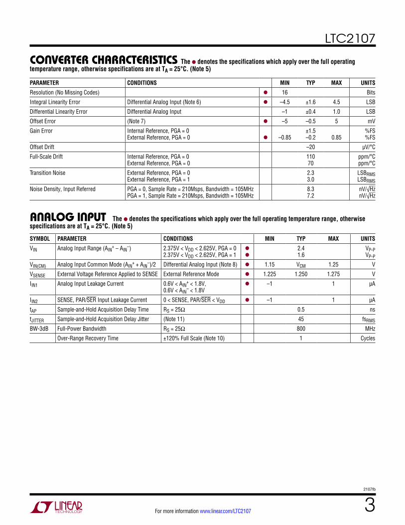
converter characteristics
analog input
The l denotes the specifications which apply over the full operating temperature range, otherwise specifications are at TA = 25°C. (Note 5)
The l denotes the specifications which apply over the full operating temperature range, otherwise specifications are at TA = 25°C. (Note 5)
PARAMETER CONDITIONS MIN TYP MAX UNITS
Resolution (No Missing Codes) l 16 Bits
Integral Linearity Error Differential Analog Input (Note 6) l –4.5 ±1.6 4.5 LSB
Differential Linearity Error Differential Analog Input –1 ±0.4 1.0 LSB
Offset Error (Note 7) l –5 –0.5 5 mV
Gain Error Internal Reference, PGA = 0 External Reference, PGA = 0
l
–0.85
±1.5 –0.2
0.85
%FS %FS
Offset Drift –20 µV/°C
Full-Scale Drift Internal Reference, PGA = 0 External Reference, PGA = 0
110 70
ppm/°C ppm/°C
Transition Noise External Reference, PGA = 0 External Reference, PGA = 1
2.3 3.0
LSBRMS LSBRMS
Noise Density, Input Referred PGA = 0, Sample Rate = 210Msps, Bandwidth = 105MHz PGA = 1, Sample Rate = 210Msps, Bandwidth = 105MHz
8.3 7.2
nV/√Hz nV/√Hz
SYMBOL PARAMETER CONDITIONS MIN TYP MAX UNITS
VIN Analog Input Range (AIN+ – AIN
–) 2.375V < VDD < 2.625V, PGA = 0 2.375V < VDD < 2.625V, PGA = 1
l
l
2.4 1.6
VP-P VP-P
VIN(CM) Analog Input Common Mode (AIN+ + AIN
–)/2 Differential Analog Input (Note 8) l 1.15 VCM 1.25 V
VSENSE External Voltage Reference Applied to SENSE External Reference Mode l 1.225 1.250 1.275 V
IIN1 Analog Input Leakage Current 0.6V < AIN+ < 1.8V,
0.6V < AIN– < 1.8V
l –1 1 µA
IIN2 SENSE, PAR/SER Input Leakage Current 0 < SENSE, PAR/SER < VDD l –1 1 µA
tAP Sample-and-Hold Acquisition Delay Time RS = 25Ω 0.5 ns
tJITTER Sample-and-Hold Acquisition Delay Jitter (Note 11) 45 fsRMS
BW-3dB Full-Power Bandwidth RS = 25Ω 800 MHz
Over-Range Recovery Time ±120% Full Scale (Note 10) 1 Cycles
LTC2107
42107fb
For more information www.linear.com/LTC2107
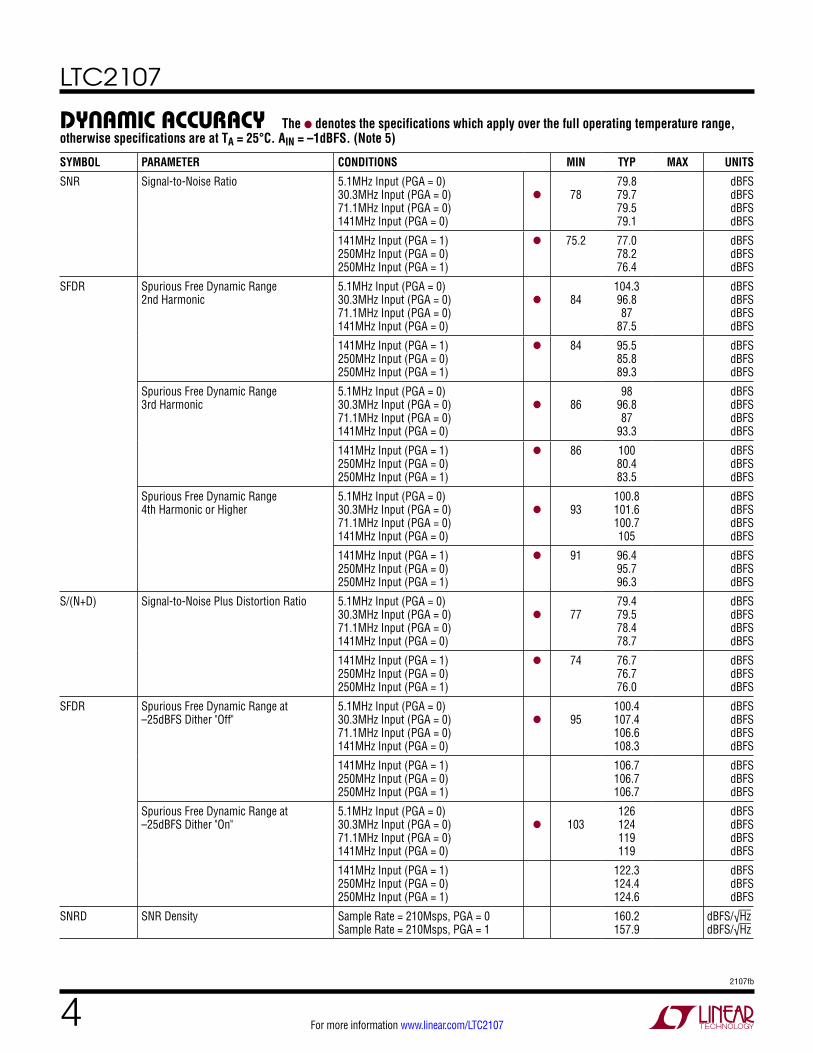
Dynamic accuracy The l denotes the specifications which apply over the full operating temperature range, otherwise specifications are at TA = 25°C. AIN = –1dBFS. (Note 5)
SYMBOL PARAMETER CONDITIONS MIN TYP MAX UNITS
SNR Signal-to-Noise Ratio 5.1MHz Input (PGA = 0) 30.3MHz Input (PGA = 0) 71.1MHz Input (PGA = 0) 141MHz Input (PGA = 0)
l
78
79.8 79.7 79.5 79.1
dBFS dBFS dBFS dBFS
141MHz Input (PGA = 1) 250MHz Input (PGA = 0) 250MHz Input (PGA = 1)
l 75.2 77.0 78.2 76.4
dBFS dBFS dBFS
SFDR Spurious Free Dynamic Range 2nd Harmonic
5.1MHz Input (PGA = 0) 30.3MHz Input (PGA = 0) 71.1MHz Input (PGA = 0) 141MHz Input (PGA = 0)
l
84
104.3 96.8 87
87.5
dBFS dBFS dBFS dBFS
141MHz Input (PGA = 1) 250MHz Input (PGA = 0) 250MHz Input (PGA = 1)
l 84 95.5 85.8 89.3
dBFS dBFS dBFS
Spurious Free Dynamic Range 3rd Harmonic
5.1MHz Input (PGA = 0) 30.3MHz Input (PGA = 0) 71.1MHz Input (PGA = 0) 141MHz Input (PGA = 0)
l
86
98 96.8 87
93.3
dBFS dBFS dBFS dBFS
141MHz Input (PGA = 1) 250MHz Input (PGA = 0) 250MHz Input (PGA = 1)
l 86 100 80.4 83.5
dBFS dBFS dBFS
Spurious Free Dynamic Range 4th Harmonic or Higher
5.1MHz Input (PGA = 0) 30.3MHz Input (PGA = 0) 71.1MHz Input (PGA = 0) 141MHz Input (PGA = 0)
l
93
100.8 101.6 100.7 105
dBFS dBFS dBFS dBFS
141MHz Input (PGA = 1) 250MHz Input (PGA = 0) 250MHz Input (PGA = 1)
l 91 96.4 95.7 96.3
dBFS dBFS dBFS
S/(N+D) Signal-to-Noise Plus Distortion Ratio 5.1MHz Input (PGA = 0) 30.3MHz Input (PGA = 0) 71.1MHz Input (PGA = 0) 141MHz Input (PGA = 0)
l
77
79.4 79.5 78.4 78.7
dBFS dBFS dBFS dBFS
141MHz Input (PGA = 1) 250MHz Input (PGA = 0) 250MHz Input (PGA = 1)
l 74 76.7 76.7 76.0
dBFS dBFS dBFS
SFDR Spurious Free Dynamic Range at –25dBFS Dither "Off"
5.1MHz Input (PGA = 0) 30.3MHz Input (PGA = 0) 71.1MHz Input (PGA = 0) 141MHz Input (PGA = 0)
l
95
100.4 107.4 106.6 108.3
dBFS dBFS dBFS dBFS
141MHz Input (PGA = 1) 250MHz Input (PGA = 0) 250MHz Input (PGA = 1)
106.7 106.7 106.7
dBFS dBFS dBFS
Spurious Free Dynamic Range at –25dBFS Dither "On"
5.1MHz Input (PGA = 0) 30.3MHz Input (PGA = 0) 71.1MHz Input (PGA = 0) 141MHz Input (PGA = 0)
l
103
126 124 119 119
dBFS dBFS dBFS dBFS
141MHz Input (PGA = 1) 250MHz Input (PGA = 0) 250MHz Input (PGA = 1)
122.3 124.4 124.6
dBFS dBFS dBFS
SNRD SNR Density Sample Rate = 210Msps, PGA = 0 Sample Rate = 210Msps, PGA = 1
160.2 157.9
dBFS/√Hz dBFS/√Hz

LTC2107
52107fb
For more information www.linear.com/LTC2107
vcm output
Digital inputs anD outputs
The l denotes the specifications which apply over the full operating temperature range, otherwise specifications are at TA = 25°C. (Note 5)
The l denotes the specifications which apply over the full operating temperature range, otherwise specifications are at TA = 25°C. (Note 5)
PARAMETER CONDITIONS MIN TYP MAX UNITS
VCM Output Voltage IOUT = 0 1.17 1.20 1.23 V
VCM Output Temperature Drift 18 ppm/°C
VCM Output Resistance –1mA < IOUT < 1mA 0.35 Ω
VCM Line Regulation 2.375V < VDD < 2.625V 0.8 mV/V
SYMBOL PARAMETER CONDITIONS MIN TYP MAX UNITS
Encode Inputs (ENC+, ENC –)
VID Differential Input Voltage (Note 8) l 0.2 2 V
VICM Common Mode Input Voltage Internally Set Externally Set (Note 8)
1.1
1.2 1.5
V V
VIN Input Voltage Range ENC+, ENC– to GND l 0 2.5 V
RIN Input Resistance (See Figure 8) 5 kΩ
RTERM Optional Encode Termination Encode Termination Enabled (See Figure 8) 107 Ω
CIN Input Capacitance Between ENC+ and ENC– (Note 8) 3 pF
Digital Inputs (CS, SDI, SCK, SHDN)
VIH High Level Input Voltage VDD = 2.5V l 1.2 V
VIL Low Level Input Voltage VDD = 2.5V l 0.6 V
IIN Input Current VIN = 0V to 3.6V l –10 10 µA
CIN Input Capacitance (Note 8) 2 pF
SDO Output (Open-Drain Output. Requires 2kΩ Pull-Up Resistor if SDO Is Used)
ROL Logic Low Output Resistance to GND VDD = 2.5V, SDO = 0V 260 Ω
IOH Logic High Output Leakage Current SDO = 0V to 3.6V l –10 10 µA
COUT Output Capacitance (Note 8) 2 pF
Digital Data Outputs (CMOS Mode)
VOH High Level Output Voltage IO = –500µA l 1.7 1.790 V
VOL Low Level Output Voltage IO = 500µA l 0.010 0.050 V
Digital Data Outputs (LVDS Mode)
VOD Differential Output Voltage 100Ω Differential Load, 3.5mA Mode 100Ω Differential Load, 1.75mA Mode
l
l
247 125
350 175
454 250
mV mV
VOS Common Mode Output Voltage 100Ω Differential Load, 3.5mA Mode 100Ω Differential Load, 1.75mA Mode
l
l
1.19 1.20
1.250 1.250
1.375 1.375
V V
RTERM On-Chip Termination Resistance Termination Enabled, OVDD = 1.8V, 3.5mA Mode 100 Ω

LTC2107
62107fb
For more information www.linear.com/LTC2107
power requirements
timing characteristics
The l denotes the specifications which apply over the full operating temperature range, otherwise specifications are at TA = 25°C. (Note 9)
The l denotes the specifications which apply over the full operating temperature range, otherwise specifications are at TA = 25°C. (Note 5)
SYMBOL PARAMETER CONDITIONS MIN TYP MAX UNITS
VDD Analog Supply Voltage (Note 9) l 2.375 2.5 2.625 V
OVDD Output Supply Voltage CMOS Mode (Note 9) LVDS Mode (Note 9)
l
l
1.7 1.7
1.8 1.8
1.9 1.9
V V
IVDD Analog Supply Current l 495.3 545 mA
IOVDD Digital Supply Current CMOS Mode LVDS Mode, 1.75mA Mode LVDS Mode, 3.5mA Mode
l
l
61 23.2 45
26 50
mA mA mA
PDISS Power Dissipation CMOS Mode LVDS Mode, 1.75mA Mode LVDS Mode, 3.5mA Mode
l
l
1348 1280 1320
1409 1453
mW mW mW
PSHDN SHDN Mode Power 6.4 mW
IVDD Analog Supply Current with Inactive Encode Encode Clock Not Active Keep Alive Oscillator Enabled
366 mA
SYMBOL PARAMETER CONDITIONS MIN TYP MAX UNITS
fS Sampling Frequency (Note 9) l 10 210 MHz
tL ENC Low Time Duty Cycle Stabilizer Off (Note 8) Duty Cycle Stabilizer On (Note 8)
l
l
2.26 1.16
2.38 2.38
50 50
ns ns
tH ENC High Time Duty Cycle Stabilizer Off (Note 8) Duty Cycle Stabilizer On (Note 8)
l
l
2.26 1.16
2.38 2.38
50 50
ns ns
tAP Sample-and-Hold Acquisition Delay Time RS = 25Ω 0.5 ns
Digital Data Outputs (CMOS Mode)
tD ENC to Data Delay CL = 6.8pF (Notes 8, 12) l 1.3 1.9 2.5 ns
tC ENC to CLKOUT Delay CL = 6.8pF (Notes 8, 12) l 1.3 1.9 2.5 ns
tSKEW DATA to CLKOUT Skew tD – tC (Note 8) l –0.3 0 0.3 ns
Pipeline Latency 7 Cycles
Digital Data Outputs (LVDS Mode)
tD ENC to Data Delay CL = 6.8pF (Notes 8, 12) l 1.3 1.9 2.5 ns
tC ENC to CLKOUT Delay CL = 6.8pF (Notes 8, 12) l 1.3 1.9 2.5 ns
tSKEW DATA to CLKOUT Skew tD – tC (Note 8) l –0.3 0 0.3 ns
Pipeline Latency 7 Cycles
SPI Port Timing (Note 8)
tSCK SCK Period Write Mode Read Back Mode, CSDO = 20pF, RPULLUP = 2k
l
l
40 250
ns ns
tCSS CS Falling to SCK Rising Setup Time l 5 ns
tSCH SCK Rising to CS Rising Hold Time l 5 ns
tSCS SCK Falling to CS Falling Setup Time l 5 ns
tDS SDI to SCK Rising Setup Time l 5 ns
tDH SCK Rising to SDI Hold Time l 5 ns
tDO SCK Falling to SDO Valid Read Back Mode, CSDO = 20pF, RPULLUP = 2k l 125 ns

LTC2107
72107fb
For more information www.linear.com/LTC2107
electrical characteristics
timing Diagrams
Note 1: Stresses beyond those listed under Absolute Maximum Ratings may cause permanent damage to the device. Exposure to any Absolute Maximum Rating condition for extended periods may affect device reliability and lifetime.Note 2: All voltage values are with respect to GND and OGND shorted (unless otherwise noted).Note 3: When these pin voltages are taken below GND or above VDD, they will be clamped by internal diodes. This product can handle input currents of greater than 100mA below GND or above VDD without latchup.Note 4: When these pin voltages are taken below GND they will be clamped by internal diodes. When these pin voltages are taken above VDD they will not be clamped by internal diodes. This product can handle input currents of greater than 100mA below GND without latchup.Note 5: VDD = 2.5V, OVDD = 1.8V, fSAMPLE = 210MHz, LVDS outputs, differential ENC+/ENC– = 2VP-P sine wave, input range = 2.4VP-P (PGA = 0) with differential drive, unless otherwise noted.
Note 6: Integral nonlinearity is defined as the deviation of a code from a best fit straight line to the transfer curve. The deviation is measured from the center of the quantization band.Note 7: Offset error is the offset voltage measured from –0.5LSB when the output code flickers between 0000 0000 0000 0000 and 1111 1111 1111 1111 in 2’s complement output mode.Note 8: Guaranteed by design, not subject to test.Note 9: Recommended operating conditions.Note 10: Refer to Overflow Bit section for additional information.Note 11: The test circuit of Figure 11 is used to verify jitter perfomance.Note 12: CL is the external single-ended load capacitance between each output pin and ground.
N-7 N-6 N-5 N-4
2107 TD01
ANALOGINPUT
ENC–
ENC+
D0-D15, OF
CLKOUT–
CLKOUT+
N
tH
tD
N+1 N+2 N+3 N+4
tAP
tC
tL
CMOS Output Timing ModeAll Outputs Are Single-Ended and Have CMOS Levels

LTC2107
82107fb
For more information www.linear.com/LTC2107
timing Diagrams
D14N-7
D15N-7
N-7 N-6 N-5 N-4
2107 TD02
N-3
D14N-6
D15N-6
D15N-5
D14N-4
D15N-4
D14N-3
D14N-5
D0N-7
ANALOGINPUT
ENC–
ENC+
D0_1+
D0_1–
D14_15+
D14_15–
OF+
OF–
CLKOUT–
CLKOUT+
D1N-7
D0N-6
D1N-6
D1N-5
D0N-4
D1N-4
D0N-3
D0N-5
N
tH
tD
N+1 N+2 N+3 N+4
tC
tL
tAP
Double Data Rate LVDS Output Mode TimingAll Outputs Are Differential and Have LVDS Levels
SPI Timing (Read-Back Mode)
SPI Timing (Write Mode)
D1D2D3D4D5D6D7A0A1A2A6 A5 A4 D0A3
tSCHtCSS
tSCS
tSCK
CS
SCK
SDI R/W
SDOHIGH IMPEDANCE
tDS
tDH
HIGHIMPEDANCE
2107 TD03
HIGH IMPEDANCED0D1D2D3D4D5D6D7
XXXXXXXXR/W A6 A5 A4 A0A1A2A3
CS
SCK
SDI
SDO
tDO
LTC2107
92107fb
For more information www.linear.com/LTC2107
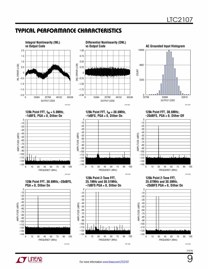
typical perFormance characteristics
128k Point FFT, fIN = 5.0MHz, –1dBFS, PGA = 0, Dither On
128k Point FFT, fIN = 30.6MHz, –1dBFS, PGA = 0, Dither On
128k Point FFT, 30.6MHz,–20dBFS, PGA = 0, Dither Off
128k Point FFT, 30.6MHz,–20dBFS, PGA = 0, Dither On
128k Point 2-Tone FFT, 25.1MHz and 30.51MHz, –7dBFS PGA = 0, Dither On
128k Point 2-Tone FFT, 25.07MHz and 30.5MHz, –20dBFS PGA = 0, Dither On
Integral Nonlinearity (INL) vs Output Code
Differential Nonlinearity (DNL) vs Output Code AC Grounded Input Histogram
OUTPUT CODE0
INL
ERRO
R (L
SB)
0
1.0
65536
2107 G01
–1.0
–2.016384 32768 49152
2.0
–0.5
0.5
–1.5
1.5
OUTPUT CODE0
DNL
ERRO
R (L
SB)
0
0.50
65536
2107 G02
–1.50
–2.0016384 32768 49152
1.00
–0.25
0.25
–1.75
0.75
FREQUENCY (MHz)0 15 30 45 60 75 90
–130
AMPL
ITUD
E (d
BFS)
–120
–100–90–80
–30–20–10
0
–60
2107 G04
–110
–50–40
–70
105FREQUENCY (MHz)
0 15 30 45 60 75 90–140
AMPL
ITUD
E (d
BFS)
–120
–100
–80
0
–40
–20
–60
–130
–110
–90
–10
–50
–30
–70
105
2107 G05
FREQUENCY (MHz)0 15 30 45 60 75 90
–140
AMPL
ITUD
E (d
BFS)
–120
–100
–80
0
–40
–20
–60
–130
–110
–90
–10
–50
–30
–70
105
2107 G06
FREQUENCY (MHz)0 15 30 45 60 75 90
–140
AMPL
ITUD
E (d
BFS)
–120
–100
–80
0
–40
–20
–60
–130
–110
–90
–10
–50
–30
–70
105
2107 G07
FREQUENCY (MHz)0 15 30 45 60 75 90
–130
AMPL
ITUD
E (d
BFS)
–120
–100–90–80
–30–20–10
0
–60
2107 G08
–110
–50–40
–70
105FREQUENCY (MHz)
0 15 30 45 60 75 90–130
AMPL
ITUD
E (d
BFS)
–120
–100–90–80
–30–20–10
0
–60
2107 G09
–110
–50–40
–70
105
OUTPUT CODE327990
COUN
T
3333
6667
10000
32809
2107 G03
32819
LTC2107
102107fb
For more information www.linear.com/LTC2107
typical perFormance characteristics
128k Point FFT, fIN = 71.1MHz, –10dBFS, PGA = 0, Dither On
128k Point FFT, fIN = 71.1MHz, –20dBFS, PGA = 0, Dither On
128k Point FFT, fIN = 71.1MHz, –20dBFS, PGA = 1, Dither On
SFDR vs Input Level, fIN = 71.1MHz, PGA = 1, Dither Off
SFDR vs Input Level, fIN = 71.1MHz, PGA = 1, Dither On
128k Point FFT, fIN = 71.1MHz and 80MHz, –7dBFS, PGA = 0, Dither On
SFDR vs Input Level, fIN = 30.6MHz, PGA = 0, Dither Off
SFDR vs Input Level, fIN = 30.6MHz, PGA = 0, Dither On
128k Point FFT, fIN = 71.1MHz, –1dBFS, PGA = 0, Dither On
INPUT LEVEL (dBFS)–80
SFDR
(dBc
AND
dBF
S)
60
120
130
140
–60 –40 –30 –20
2107 G10
40
100
80
50
110
30
90
70
–70 –50 –10 0
dBFS
dBc
INPUT LEVEL (dBFS)–80
SFDR
(dBc
AND
dBF
S)
60
120
130
140
–60 –40 –30 –20
2107 G11
40
100
80
50
110
30
90
70
–70 –50 –10 0
dBFS
dBc
FREQUENCY (MHz)0 15 30 45 60 75 90
–130
AMPL
ITUD
E (d
BFS)
–120
–100–90–80
–30–20–10
0
–60
2107 G12
–110
–50–40
–70
105
FREQUENCY (MHz)0 15 30 45 60 75 90
–130
AMPL
ITUD
E (d
BFS)
–120
–100–90–80
–30–20–10
0
–60
2107 G13
–110
–50–40
–70
105FREQUENCY (MHz)
0 15 30 45 60 75 90–130
AMPL
ITUD
E (d
BFS)
–120
–100–90–80
–30–20–10
0
–60
2107 G14
–110
–50–40
–70
105FREQUENCY (MHz)
0 15 30 45 60 75 90–130
AMPL
ITUD
E (d
BFS)
–120
–100–90–80
–30–20–10
0
–60
2107 G15
–110
–50–40
–70
105
INPUT LEVEL (dBFS)–80
SFDR
(dBc
AND
dBF
S)
60
120
130
140
–60 –40 –30 –20
2107 G16
40
100
80
50
110
30
90
70
–70 –50 –10 0
dBFS
dBc
INPUT LEVEL (dBFS)–80
SFDR
(dBc
AND
dBF
S)
60
120
130
140
–60 –40 –30 –20
2107 G17
40
100
80
50
110
30
90
70
–70 –50 –10 0
dBFS
dBc
FREQUENCY (MHz)0 15 30 45 60 75 90
–130
AMPL
ITUD
E (d
BFS)
–120
–100–90–80
–30–20–10
0
–60
2107 G18
–110
–50–40
–70
105
LTC2107
112107fb
For more information www.linear.com/LTC2107
typical perFormance characteristics
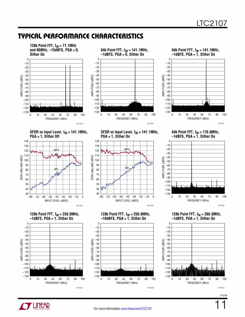
SFDR vs Input Level, fIN = 141.1MHz, PGA = 1, Dither Off
SFDR vs Input Level, fIN = 141.1MHz, PGA = 1, Dither On
64k Point FFT, fIN = 170.0MHz, –1dBFS, PGA = 1, Dither On
128k Point FFT, fIN = 250.0MHz, –1dBFS, PGA = 1, Dither On
128k Point FFT, fIN = 250.0MHz, –10dBFS, PGA = 1, Dither On
128k Point FFT, fIN = 380.0MHz, –1dBFS, PGA = 1, Dither On
128k Point FFT, fIN = 71.1MHz and 80MHz, –15dBFS, PGA = 0, Dither On
64k Point FFT, fIN = 141.1MHz, –1dBFS, PGA = 0, Dither On
64k Point FFT, fIN = 141.1MHz, –1dBFS, PGA = 1, Dither On
FREQUENCY (MHz)0 15 30 45 60 75 90
–130
AMPL
ITUD
E (d
BFS)
–120
–100–90–80
–30–20–10
0
–60
2107 G19
–110
–50–40
–70
105FREQUENCY (MHz)
0 15 30 45 60 75 90–130
AMPL
ITUD
E (d
BFS)
–120
–100–90–80
–30–20–10
0
–60
2107 G20
–110
–50–40
–70
105FREQUENCY (MHz)
0 15 30 45 60 75 90–130
AMPL
ITUD
E (d
BFS)
–120
–100–90–80
–30–20–10
0
–60
2107 G21
–110
–50–40
–70
105
INPUT LEVEL (dBFS)–80
SFDR
(dBc
AND
dBF
S)
60
120
130
140
–60 –40 –30 –20
2107 G22
40
100
80
50
110
30
90
70
–70 –50 –10 0
dBFS
dBc
INPUT LEVEL (dBFS)–80
SFDR
(dBc
AND
dBF
S)
60
120
130
140
–60 –40 –30 –20
2107 G23
40
100
80
50
110
30
90
70
–70 –50 –10 0
dBFS
dBc
FREQUENCY (MHz)0 15 30 45 60 75 90
–130
AMPL
ITUD
E (d
BFS)
–120
–100–90–80
–30–20–10
0
–60
2107 G24
–110
–50–40
–70
105
FREQUENCY (MHz)0 15 30 45 60 75 90
–130
AMPL
ITUD
E (d
BFS)
–120
–100–90–80
–30–20–10
0
–60
2107 G25
–110
–50–40
–70
105FREQUENCY (MHz)
0 15 30 45 60 75 90–130
AMPL
ITUD
E (d
BFS)
–120
–100–90–80
–30–20–10
0
–60
2107 G26
–110
–50–40
–70
105FREQUENCY (MHz)
0 15 30 45 60 75 90–130
AMPL
ITUD
E (d
BFS)
–120
–100–90–80
–30–20–10
0
–60
2107 G27
–110
–50–40
–70
105

LTC2107
122107fb
For more information www.linear.com/LTC2107
typical perFormance characteristics
SNR and SFDR vs Sample Rate, fIN = 5MHz, –1dBFSSNR vs Input Frequency
SNR and SFDR vs Supply Voltage (VDD), fIN = 5MHz, –1dBFS
IVDD vs Sample Rate, 5MHz Sine Wave, –1dBFS
Normalized Full Scale vs Temperature, Internal Reference, 5 Units
Normalized Full Scale vs Temperature, External Reference, 5 Units
128k Point FFT, fIN = 380.0MHz, –10dBFS, PGA = 1, Dither On
HD2/HD3 vs Input Frequency, PGA = 0, –1dBFS
HD2/HD3 vs Input Frequency, PGA = 1, –1dBFS
FREQUENCY (MHz)0 15 30 45 60 75 90
–130
AMPL
ITUD
E (d
BFS)
–120
–100–90–80
–30–20–10
0
–60
2107 G28
–110
–50–40
–70
105
TEMPERATURE (°C)–40
0.990
NORM
ALIZ
ED F
ULL
SCAL
E
0.995
1.000
1.005
1.010
–20 0 20 40
2107 G35
60 80TEMPERATURE (°C)
–400.990
NORM
ALIZ
ED F
ULL
SCAL
E
0.995
1.000
1.005
1.010
–20 0 20 40
2107 G36
60 80
INPUT FREQUENCY (MHz)0
dBFS
100
110
120
200
2107 G29
90
80
7050 100 150 250
HD3HD2
INPUT FREQUENCY (MHz)0
dBFS
100
110
120
200
2107 G30
90
80
7050 100 150 250
HD3HD2
INPUT FREQUENCY (MHz)1
74
SNR
(dBF
S)
75
76
77
78
79
80
100 200 300 400
2107 G31
500
PGA = 0
PGA = 1
SAMPLE RATE (Msps)0 30
60
SNR
AND
SFDR
(dBF
S)
80
70
60 180
110
100
90
90 120 150 210
2107 G32
SFDR
SNR
SUPPLY VOLTAGE (VDD)2.3
SNR
AND
SFDR
(dBF
S)
90
100
2.7
2107 G33
80
702.4 2.5 2.6
110
SFDRSNR
VDD(MIN) = 2.375V
VDD(MAX) = 2.625V
SAMPLE RATE (Msps)
350
I VDD
(mA)
400
450
500
0 30 60 90 120
2107 G34
150 180 210
LTC2107
132107fb
For more information www.linear.com/LTC2107
typical perFormance characteristics
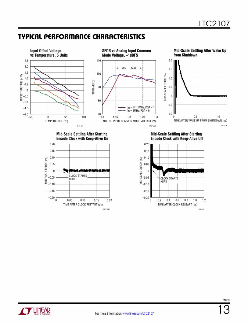
Mid-Scale Settling After Starting Encode Clock with Keep-Alive On
Mid-Scale Settling After Starting Encode Clock with Keep-Alive Off
Input Offset Voltage vs Temperature, 5 Units
SFDR vs Analog Input Common Mode Voltage, –1dBFS
Mid-Scale Settling After Wake Up from Shutdown
TEMPERATURE (°C)–50
–2.0
OFFS
ET V
OLTA
GE (m
V)
–1.5
–0.5
0
0.5
50
2.5
2107 G37
–1.0
0 100
1.0
1.5
2.0
TIME AFTER WAKE UP FROM SHUTDOWN (µs)0
–1.0
MID
-SCA
LE E
RROR
(%)
–0.5
0
0.5
1.0
1.5
2.0
0.5 1.0
2107 G39
TIME AFTER CLOCK RESTART (µs)0
MID
-SCA
LE E
RROR
(%)
0
0.05
0.10
0.20
2107 G40
–0.05
–0.10
–0.200.05 0.10 0.15
–0.15
0.20
0.15
CLOCK STARTSHERE
TIME AFTER CLOCK RESTART (µs)0
MID
-SCA
LE E
RROR
(%)
0
2107 G41
–0.10
–0.200.4 0.80.2 0.6 1.0
0.10
0.20
–0.05
–0.15
0.05
0.15
1.2
CLOCK STARTSHERE
ANALOG INPUT COMMON MODE VOLTAGE (V)1.1
SFDR
(dBF
S)
90
100
1.3
2107 G38
80
701.15 1.2 1.25
110
MIN MAX
fIN = 141.1MHz, PGA = 1fIN = 5MHz, PGA = 0

LTC2107
142107fb
For more information www.linear.com/LTC2107
pin Functions(Pins That Are the Same for All Digital Output Modes)
SENSE (Pin 1): Reference Programming Pin. The SENSE pin voltage selects the use of an internal reference or an external 1.25V reference. Connecting SENSE to ground or VDD selects the internal reference. Connect SENSE to a 1.25V external reference and the external reference mode is automatically selected. The external reference must be 1.25V ±25mV for proper operation.
GND (Pins 2, 3, 7, 10, 12, 13, 16, 47, 48, 49): ADC Power Ground.
VDD (Pins 4, 5, 6): 2.5V Analog Power Supply. Bypass to ground with an 0402 10µF ceramic capacitor and an 0402 0.1µF ceramic capacitor as close to these pins as possible. Pins 4, 5 and 6 can share these two bypass capacitors.
AIN+ (Pin 8): Positive Differential Analog Input.
AIN– (Pin 9): Negative Differential Analog Input.
VCM (Pin 11): Common Mode Bias Output, Nominally Equal to 1.2V. VCM should be used to bias the common mode of the analog inputs. Bypass to ground with a 2.2µF ceramic capacitor.
ENC+ (Pin 14): Encode Input. Conversion starts on the rising edge.
ENC– (Pin 15): Encode Complement Input. Conversion starts on the falling edge.
SHDN (Pin 17): Power Shutdown Pin. SHDN = 0V results in normal operation. SHDN = 2.5V results in powered-down analog circuitry and the digital outputs are set in high impedance state.
SDO (Pin 18): In serial programming mode, (PAR/SER = 0V), SDO is the serial interface data output. Data on SDO is read back from the mode control registers and can be latched on the falling edge of SCK. SDO is an open-drain NMOS output that requires an external 2k pull-up resistor to 1.8V-3.3V. If readback from the mode control registers is not needed, the pull-up resistor is not necessary and SDO can be left unconnected.
OGND (Pins 19, 42): Output Driver Ground. OGND and GND should be tied together with a common ground plane.
OVDD (Pins 20, 41): 1.8V Output Driver Supply. Bypass each OVDD pin to ground with an 0402 1µF ceramic capaci-tor and an 0402 0.1µF ceramic capacitor. Place the bypass capacitors as close to these pins as possible. Pins 20 and 41 cannot share these bypass capacitors.
SDI (Pin 43): In serial programming mode, (PAR/SER = 0V), SDI is the serial interface data input. Data on SDI is clocked into the mode control registers on the rising edge of SCK. In the parallel programming mode (PAR/SER = VDD), SDI becomes the digital output randomization control bit. When SDI is low, digital output randomization is disabled. When SDI is high, digital output randomization is enabled. SDI can be driven with 1.8V to 3.3V logic.
SCK (Pin 44): In serial programming mode, (PAR/SER = 0V), SCK is the serial interface clock input. In the parallel programming mode (PAR/SER = VDD), SCK controls the programmable gain amplifier front-end, PGA. SCK low selects a front-end gain of 1, input range of 2.4VP-P. High selects a front-end gain of 1.5, input range of 1.6VP-P. SCK can be driven with 1.8V to 3.3V logic.
CS (Pin 45): In serial programming mode, (PAR/SER = 0V), CS is the serial interface chip select input. When CS is low, SCK is enabled for shifting data on SDI into the mode control registers. In the parallel programming mode (PAR/SER = VDD), CS controls the digital output mode. When CS is low, the full-rate CMOS output mode is enabled. When CS is high, the double data rate LVDS output mode (with 3.5mA output current) is enabled. CS can be driven with 1.8V to 3.3V logic.
PAR/SER (Pin 46): Programming Mode Selection Pin. Connect to ground to enable the serial programming mode. CS, SCK, SDI, SDO become a serial interface that control the A/D operating modes. Connect to VDD to enable the parallel programming mode where CS, SCK, SDI become parallel logic inputs that control a reduced set of the A/D operating modes. PAR/SER should be connected directly to ground or the VDD of the part and not be driven by a logic signal.

LTC2107
152107fb
For more information www.linear.com/LTC2107
pin FunctionsFull-Rate CMOS Output Mode
All pins below have CMOS output levels (OGND to OVDD)
CMOS Output Mode is only recommended for sample rates up to 100Msps.
D0-D15 (Pins 21-30, 33-38): Digital Outputs. D15 is the MSB.
CLKOUT– (Pin 31): Inverted Version of CLKOUT+.
CLKOUT+ (Pin 32): Data Output Clock. The digital outputs normally transition at the same time as the falling edge of CLKOUT+. The phase of CLKOUT+ can also be delayed relative to the digital outputs by programming the mode control registers.
DNC (Pin 39): Do not connect this pin.
OF (Pin 40): Over/Under Flow Digital Output. OF is high when an overflow or underflow has occurred.
Double Data Rate LVDS Output Mode
All pins below have LVDS output levels. The output current level is programmable. There is an optional internal 100Ω termination resistor between the pins of each LVDS output pair.
D0_1–/D0_1+ to D14_15–/D14_15+ (Pins 21/22, 23/24, 25/26, 27/28, 29/30, 33/34, 35/36, 37/38): Double Data Rate Digital Outputs. Two data bits are multiplexed onto each differential output pair. The even data bits (D0, D2, D4, D6, D8, D10, D12, D14) appear when CLKOUT+ is low. The odd data bits (D1, D3, D5, D7, D9, D11, D13, D15) appear when CLKOUT+ is high.
CLKOUT–/CLKOUT+ (Pins 31/32): Data Output Clock. The digital outputs normally transition at the same time as the falling and rising edges of CLKOUT+. The phase of CLKOUT+ can also be delayed relative to the digital outputs by programming the mode control registers.
OF–/OF+ (Pins 39/40): Over/Under Flow Digital Output. OF+ is high when an overflow or underflow has occurred.OF– is an inverted version of OF+.
LTC2107
162107fb
For more information www.linear.com/LTC2107
Block Diagram
–
+INPUT
S/H
CORRECTION LOGICAND
SHIFT REGISTER
OUTPUTBUFFERS
PIPELINEADC
STAGE6
16CLKOUT
OGND
2107 F01
D14_15±•••
D0_1±
1.8V
AIN–
AIN+
VCM
BUFFER ADCREFERENCE
OF
OVDD
2.5VVDD
GND
ENC+ ENC–
CLOCK ANDCLOCK CONTROL
PAR/SER SDI SCK CS SDO SHDN
ADC CONTROL/SPI INTERFACE
PIPELINEADC
STAGE5
PIPELINEADC
STAGE4
PIPELINEADC
STAGE3
PIPELINEADC
STAGE2
PIPELINEADC
STAGE1
DITHERSIGNAL
GENERATOR
INTERNALVOLTAGE
REFERENCE
SENSE
RANGESELECT
PGA
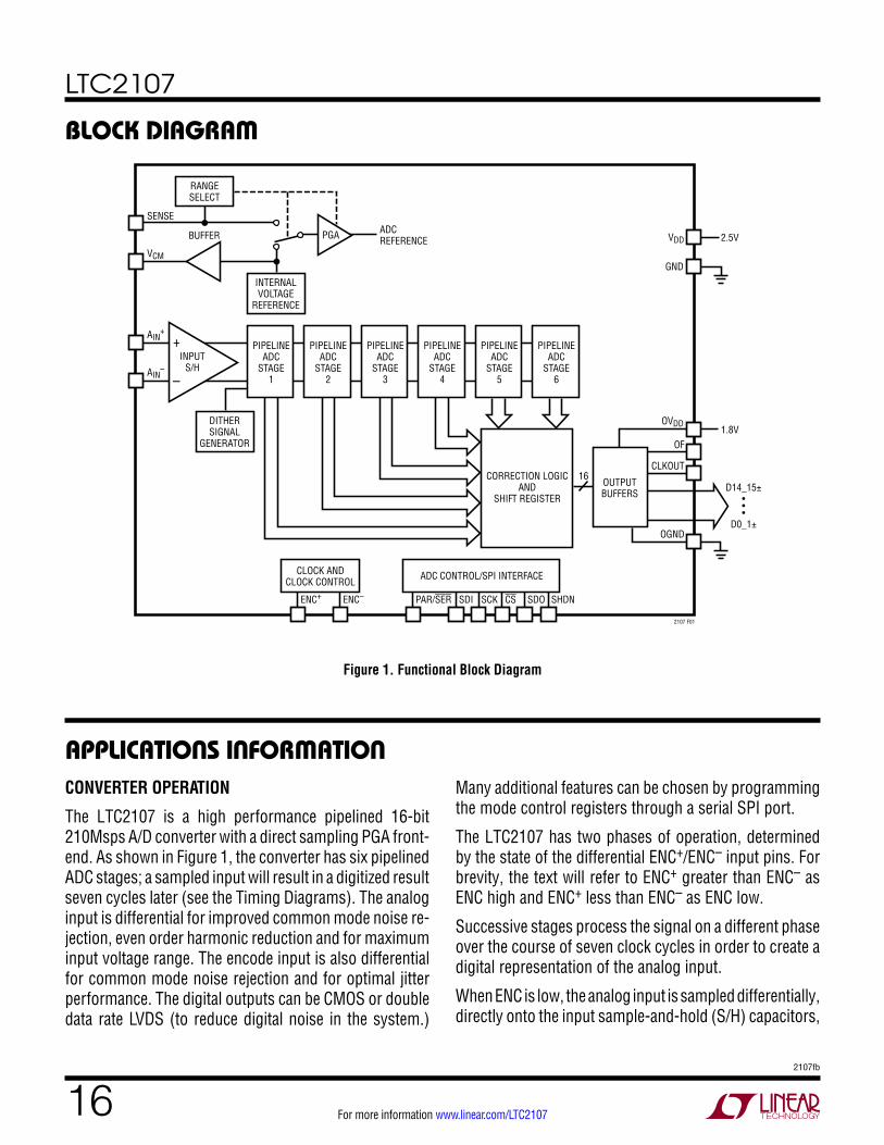
Figure 1. Functional Block Diagram
applications inFormationCONVERTER OPERATION
The LTC2107 is a high performance pipelined 16-bit 210Msps A/D converter with a direct sampling PGA front-end. As shown in Figure 1, the converter has six pipelined ADC stages; a sampled input will result in a digitized result seven cycles later (see the Timing Diagrams). The analog input is differential for improved common mode noise re-jection, even order harmonic reduction and for maximum input voltage range. The encode input is also differential for common mode noise rejection and for optimal jitter performance. The digital outputs can be CMOS or double data rate LVDS (to reduce digital noise in the system.)
Many additional features can be chosen by programming the mode control registers through a serial SPI port.
The LTC2107 has two phases of operation, determined by the state of the differential ENC+/ENC– input pins. For brevity, the text will refer to ENC+ greater than ENC– as ENC high and ENC+ less than ENC– as ENC low.
Successive stages process the signal on a different phase over the course of seven clock cycles in order to create a digital representation of the analog input.
When ENC is low, the analog input is sampled differentially, directly onto the input sample-and-hold (S/H) capacitors,

LTC2107
172107fb
For more information www.linear.com/LTC2107
applications inFormation
AIN+
LPAR0.7nH
CPAR0.66pF
RON5.6Ω
VDDLTC2107
1.8Ω
CSAMPLE5.72pF
AIN–
ENC+
LPAR0.7nH
CPAR0.66pF
5k
5k
VDD/2
VDD/2
2107 F02
VDD
RON5.6Ω
VDD
1.8Ω
CSAMPLE5.72pF
ENC–
Figure 2. Equivalent Input Circuit
inside the “Input S/H” shown in the Block Diagram. At the instant the ENC transitions from low to high, the voltage on the sample capacitors is held. While ENC is high, the held input voltage is buffered by the S/H amplifier which drives the first pipelined ADC stage. The first stage acquires the output of the S/H amplifier during the high phase of ENC. When ENC goes back low, the first stage produces its output which is acquired by the second stage. At the same time, the input S/H goes back to acquiring the next analog input. When ENC goes back high again, the second stage produces its output which is acquired by the third stage. The identical process is repeated for the remaining stages 3-5 finally resulting in an output at the output of the 5th stage which is sent to the 6th ADC stage for final evaluation.
Results from all stages are digitally delayed such that stage results are aligned with one analog input sample. The delayed results from all stages are then combined in the correction logic and the final result is sent to the output buffers.
SAMPLE/HOLD OPERATION
Figure 2 shows the equivalent circuit for the LTC2107 direct sampling, differential sample/hold circuit. The dif-ferential analog inputs, AIN
+ and AIN– are sampled directly
on to the sampling capacitors (CSAMPLE) through NMOS transistor switches. The capacitors shown attached to each input (CPAR) are the summation of all other capacitance associated with each input, for interconnect and device parasitics.
During the sample phase, when ENC is low, the NMOS switches connect the analog inputs to the sampling capaci-tors, such that they charge to, and track the input voltage. The capacitance seen at the input during the sample phase is the sum of CSAMPLE and CPAR or 6.38pF. When ENC transitions from low to high, the NMOS switches open, disconnecting the analog inputs from the sampling capaci-tors. The voltage on the sampling capacitors is held and is passed to the ADC core for evaluation. The capacitance seen at the input during the hold phase is CPAR or 0.66pF.
Sampling Glitch
As ENC transitions from high to low, the inputs are re-connected to the sampling capacitors to acquire a new sample. Since the sampling capacitors still hold the pre-vious sample, the analog inputs must supply a charge that is proportional to the change in voltage between the current sample and the previous sample. Additionally there is a fixed charge associated with the turn-on of the NMOS sampling switches.
Ideally, the input circuitry should be fast enough to fully charge the sampling capacitor during the sampling period 1/2fENCODE. However, this is not always possible and the incomplete settling may degrade the SFDR. The sampling glitch has been designed to be as linear as possible to minimize the effects of incomplete settling.
LTC2107
182107fb
For more information www.linear.com/LTC2107
applications inFormationParticular care has to be taken when driving the ADC with test equipment involving long BNC cables. Such a situation can create reflections in the BNC cable which will degrade SFDR. Connecting a 3dB attenuator pad at the input to the demo board will help mitigate this problem.
Drive Impedance
As with all high performance, high speed ADCs the dy-namic performance of the LTC2107 can be influenced by the input drive circuitry, particularly the second and third harmonics. Source impedance and input reactance can influence SFDR. At the falling edge of ENC the sample and hold circuit will connect the 5.72pF sampling capacitor to the input pin and start the sampling period. The sampling period ends when ENC rises, holding the sampled input on the sampling capacitor.
The analog input drive impedance will affect sampling bandwidth and settling time. The input impedance of the LTC2107 is primarily capacitive for frequencies below 1GHz. Higher source impedance will result in slower settling and lower sampling bandwidth. The sampling bandwidth is typically 800MHz with a source impedance of 25Ω.
Better SFDR results from lower input impedance. For the best performance it is recommended to have a source impedence of 50Ω or less for each input. The source impedance should be matched for the differential inputs. Poor matching will result in higher even order harmonics, especially the second.
PGA Function
The LTC2107 has a programmable gain amplifier sample/hold circuit. The gain can be controlled through the serial or parallel modes of operation. PGA = 0 selects a sample/hold gain of 1 and an input range of 2.4VP-P. PGA = 1 selects a sample/hold gain of 1.5 and an input range of 1.6VP-P. The PGA setting allows flexibility for ADC drive optimization. A lower ADC input signal eases the OIP3 requirements of the ADC driver circuit.The lower input range of the PGA = 1 setting is easier to drive and has lower distortion for high frequency applications. For PGA = 1, SNR is lower by 2.3dB as compared to PGA = 0; however the input referred noise is improved by 1.2dB.
Table 1. PGA settingsPGA = 0 PGA = 1 UNIT
Input Range 2.4 1.6 VP-P
SNR, Idle Channel 80 77.7 dBFS
Input Referred Noise 85 74 µVRMS
INPUT DRIVE CIRCUITS
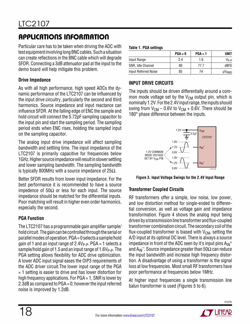
The inputs should be driven differentially around a com-mon mode voltage set by the VCM output pin, which is nominally 1.2V. For the 2.4V input range, the inputs should swing from VCM – 0.6V to VCM + 0.6V. There should be 180° phase difference between the inputs.
VCM2.2µF
1.2V
1.8V
1.2V
0.6V
1.8V
1.2V COMMONMODE VOLTAGESET BY VCM PIN
1.2V
0.6V
AIN+
AIN+
LTC2107
2107 F03
Figure 3. Input Voltage Swings for the 2.4V Input Range
Transformer Coupled Circuits
RF transformers offer a simple, low noise, low power, and low distortion method for single-ended to differen-tial conversion, as well as voltage gain and impedance transformation. Figure 4 shows the analog input being driven by a transmission line transformer and flux-coupled transformer combination circuit. The secondary coil of the flux-coupled transformer is biased with VCM, setting the A/D input at its optimal DC level. There is always a source impedance in front of the ADC seen by it’s input pins AIN
+ and AIN
–. Source impedance greater than 50Ω can reduce the input bandwidth and increase high frequency distor-tion. A disadvantage of using a transformer is the signal loss at low frequencies. Most small RF transformers have poor performance at frequencies below 1MHz.
At higher input frequencies a single transmission line balun transformer is used (Figures 5 to 6).

LTC2107
192107fb
For more information www.linear.com/LTC2107
Figure 4. Single-Ended to Differential Conversion Using Two Transformers. Recommended for Input Frequencies from 5MHz to 100MHz
applications inFormation
Figure 5. Single-Ended to Differential Conversion Using Two Transformers. Recommended for Input Frequencies from 100MHz to 250MHz
Figure 6. Single-Ended to Differential Conversion Using One Transformer. Recommended for Input Frequencies Above 250MHz
VCM
AIN+
2.2µF0.1µF
10pF
0.1µF
WBC1-TLB0.1µF
ANALOGINPUT
10Ω
20Ω
200Ω
AIN+
20ΩLTC2107
MABA-007159-000000 ••••
31.6Ω
31.6Ω
2107 F04
VCM
AIN+
2.2µF0.1µF
10pF
0.1µF
0.1µFANALOG
INPUT
10Ω
20Ω
200Ω
AIN+
20ΩLTC2107
MABA-007159-000000
••
MABA-007159-000000
••31.6Ω
31.6Ω
2107 F05
VCM
AIN+
2.2µF0.1µF
4.7pF
0.1µF
0.1µFANALOG
INPUT
10Ω
5Ω10Ω
10Ω
AIN+
5ΩLTC2107
MABA-007159-000000
••25Ω
25Ω
2107 F06
Dither
The dither function enhances the SFDR performance of the LTC2107. Dither can be turned on by writing a “1” to register A1[2]. For brevity, the text will refer to AIN
+ – AIN
– as AIN. The dither function adds a pseudorandom dither voltage to the sampled analog input at the front of
the ADC, yielding AIN + dither. This signal is converted by the ADC, yielding AIN + dither in digital format. Dither is then subtracted, yielding the AIN value at the output of the ADC in 16 bit resolution. The dither function is invisible to the user. The input signal range of the ADC is not affected when dither is turned on.
Reference
The LTC2107 has an internal 1.25V voltage reference.Connecting SENSE to VDD or GND selects use of the in-ternal 1.25V reference. The SENSE pin is also the input for an external 1.25V reference. Figure 7 shows how an external 1.25V reference voltage or the internal 1.25V reference can be used. Figure 8 shows how an external 1.25V reference voltage can be configured. Either internal or external reference will result in an ADC input range of 2.4VP-P with PGA = 0.

LTC2107
202107fb
For more information www.linear.com/LTC2107
applications inFormation
Encode Input
The signal quality of the differential encode inputs strongly affects the A/D noise performance. The encode inputs should be treated as analog signals—do not route them next to digital traces on the circuit board. Sinusoidal, PECL, or LVDS encode inputs can be used. The encode inputs are internally biased to 1.25V through 5k equivalent resistance. An optional 100Ω termination resistor can be
Figure 12. PECL or LVDS Encode Drive
Figure 11. Sinusoidal Encode Drive
turned on by writing a “1” to control register bit A3[5]. The encode inputs can be taken up to VDD, and the common mode range is from 1.1V to 1.5V.
For good jitter performance a high quality, low jitter clock source should be used. A 2VP-P differential encode signal is recommended for optimum SNR performance. Refer to Figure 10 for clock source jitter requirements to achieve a desired SNR at a given input frequency.
Figure 9. Equivalent Encode Input Circuit
Figure 10. Ideal SNR Versus Analog Input Frequency and Clock Source Jitter
5k
5k
ENC+
LTC2107
ENC–
OPTIONAL 100ΩTERMINATION
1.25V
VDDDIFFERENTIALCOMPARATOR
1.25V
2107 F08
ANALOG INPUT FREQUENCY (MHz)10
55SN
R (d
BFS)
60
65
70
75
85
100 1000
2107 F10
80
0fsRMS50fsRMS100fsRMS200fsRMS
ADDITIVEJITTER
24.9Ω
24.9Ω
2107 F11
0.1µF
10Ω
2VP-P
10Ω
0.1µFSINEWAVE
INPUT
MABA-007159-000000
BANDPASS FILTER(RECOMMENDED FOR LOW NOISE APPLICATIONS)
••
0.1µF
LT2107
ENC+
ENC–
2VP-P
0.1µF
CAPACITORS 0402PACKAGE SIZE
PECL ORLVDS
CLOCKENC–
2107 F12
0.1µFENC+
LTC2107
Figure 8. Using an external 1.25V reference.
LTC2107
VCM
SENSE
25k
VDD
LT1634-1.25
2.2µF
0.1µF2107 F08
Figure 7. Reference Circuit.
INTERNALADCREFERENCE
TIE SENSE TO 0V OR VDD TO USETHE INTERNAL 1.25V REFERENCETIE SENSE TO A 1.25V REFERENCETO USE AN EXTERNAL REFERENCE
REFERENCESELECTION
CIRCUIT
1.2V
SENSE
LTC2107
1.25VVCM
BUFFER
2.2µF
2107 F07
1.25VBANDGAP
REFERENCE
LTC2107
212107fb
For more information www.linear.com/LTC2107
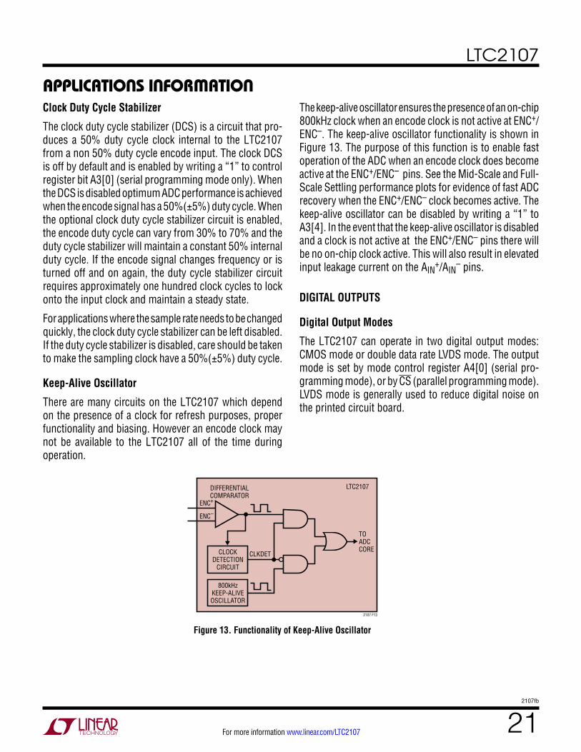
Figure 13. Functionality of Keep-Alive Oscillator
applications inFormationClock Duty Cycle Stabilizer
The clock duty cycle stabilizer (DCS) is a circuit that pro-duces a 50% duty cycle clock internal to the LTC2107 from a non 50% duty cycle encode input. The clock DCS is off by default and is enabled by writing a “1” to control register bit A3[0] (serial programming mode only). When the DCS is disabled optimum ADC performance is achieved when the encode signal has a 50%(±5%) duty cycle. When the optional clock duty cycle stabilizer circuit is enabled, the encode duty cycle can vary from 30% to 70% and the duty cycle stabilizer will maintain a constant 50% internal duty cycle. If the encode signal changes frequency or is turned off and on again, the duty cycle stabilizer circuit requires approximately one hundred clock cycles to lock onto the input clock and maintain a steady state.
For applications where the sample rate needs to be changed quickly, the clock duty cycle stabilizer can be left disabled. If the duty cycle stabilizer is disabled, care should be taken to make the sampling clock have a 50%(±5%) duty cycle.
Keep-Alive Oscillator
There are many circuits on the LTC2107 which depend on the presence of a clock for refresh purposes, proper functionality and biasing. However an encode clock may not be available to the LTC2107 all of the time during operation.
The keep-alive oscillator ensures the presence of an on-chip 800kHz clock when an encode clock is not active at ENC+/ENC–. The keep-alive oscillator functionality is shown in Figure 13. The purpose of this function is to enable fast operation of the ADC when an encode clock does become active at the ENC+/ENC– pins. See the Mid-Scale and Full-Scale Settling performance plots for evidence of fast ADC recovery when the ENC+/ENC– clock becomes active. The keep-alive oscillator can be disabled by writing a “1” to A3[4]. In the event that the keep-alive oscillator is disabled and a clock is not active at the ENC+/ENC– pins there will be no on-chip clock active. This will also result in elevated input leakage current on the AIN
+/AIN– pins.
DIGITAL OUTPUTS
Digital Output Modes
The LTC2107 can operate in two digital output modes: CMOS mode or double data rate LVDS mode. The output mode is set by mode control register A4[0] (serial pro-gramming mode), or by CS (parallel programming mode). LVDS mode is generally used to reduce digital noise on the printed circuit board.
TOADCCORE
CLKDET
2107 F13
ENC+
LTC2107
ENC–
DIFFERENTIALCOMPARATOR
CLOCKDETECTION
CIRCUIT
800kHzKEEP-ALIVEOSCILLATOR

LTC2107
222107fb
For more information www.linear.com/LTC2107
applications inFormationCMOS Mode
In CMOS mode the 16 digital outputs (D0-D15), overflow (OF), and the data output clocks (CLKOUT+, CLKOUT –) have CMOS output levels. The outputs are powered by OVDD and OGND which are isolated from the A/D core power and ground.
For good performance the digital outputs should drive minimal capacitive loads. If the load capacitance is larger than 5pF a digital buffer should be used.
CMOS mode is not recommended for sampling rates greater that 100Msps.
Double Data Rate LVDS Mode
In double data rate LVDS mode, two data bits are multi-plexed and output on each differential output pair. There are eight LVDS ADC data output pairs: (D0_1+/D0_1– through D14_15+/D14_15–). Overflow (OF+/OF–) and the data output clock (CLKOUT+/CLKOUT–) each have an LVDS output pair.
By default the outputs are standard LVDS levels: 3.5mA output current and a 1.25V output common mode volt-age. An external 100Ω differential termination resistor is required for each LVDS output pair. The termination resistors should be located as close as possible to the LVDS receiver.
The outputs are powered by OVDD and OGND which are isolated from the A/D core power and ground. In LVDS mode, OVDD should be 1.8V.
Programmable LVDS Output Current
In LVDS Mode, the default output driver current is 3.5mA. This current can be adjusted by serially programming mode control register A4. Available current levels are 1.75mA, 2.1mA, 2.5mA, 3mA, 3.5mA, 4mA and 4.5mA.
Optional LVDS Driver Internal Termination
In most cases using just an external 100Ω termination resistor will give excellent LVDS signal integrity. In addi-tion, an optional internal 100Ω termination resistor can be enabled by serially programming mode control register A4[3]. The internal termination helps absorb any reflections caused by imperfect termination at the receiver. When the internal termination is enabled, the output driver current is doubled to maintain the same output voltage swing.
Overflow Bit
The overflow output bit (OF) outputs a logic high when the analog input is either overranged or underranged. The overflow bit has the same pipeline latency as the data bits.
In Full-Rate CMOS mode OF is the overflow pin. In DDR LVDS mode OF–/OF+ are the two differential overflow pins. Sustained over-range or under-range beyond 120% of full-scale, for more than 20,000 samples may produce erroneous ADC codes and an extended ADC recovery time.
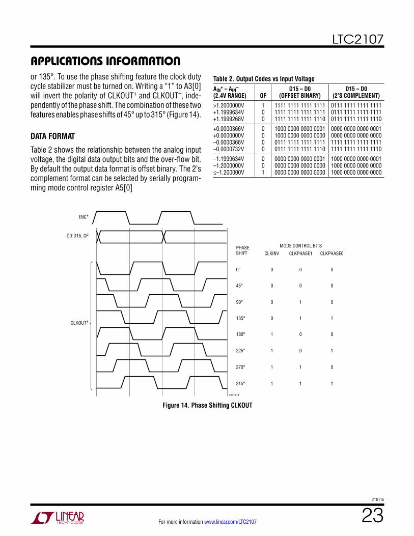
Phase Shifting the Output Clock
In full rate CMOS mode the data output bits normally change at the same time as the falling edge of CLKOUT+, so the rising edge of CLKOUT+ can be used to latch the output data. In double data rate LVDS mode the data output bits normally change at the same time as the falling and rising edges of CLKOUT+. To allow adequate setup and hold time when latching the data, the CLKOUT+ signal may need to be phase shifted relative to the data output bits. Most FPGAs have this feature—this is generally the best place to adjust the timing.
The LTC2107 can also phase shift the CLKOUT+/CLKOUT– signals by serially programming mode control register A3[2:1]. The output clock can be shifted by 0°, 45°, 90°,
LTC2107
232107fb
For more information www.linear.com/LTC2107
applications inFormationor 135°. To use the phase shifting feature the clock duty cycle stabilizer must be turned on. Writing a “1” to A3[0] will invert the polarity of CLKOUT+ and CLKOUT–, inde-pendently of the phase shift. The combination of these two features enables phase shifts of 45° up to 315° (Figure 14).
DATA FORMAT
Table 2 shows the relationship between the analog input voltage, the digital data output bits and the over-flow bit. By default the output data format is offset binary. The 2’s complement format can be selected by serially program-ming mode control register A5[0]
PHASESHIFT
0° 0 0 0
45° 0 0 0
90° 0 1 0
135° 0 1 1
180°
CLKOUT+
D0-D15, OF
ENC+
1 0 0
225° 1 0 1
270° 1 1 0
315°
2107 F14
1 1 1
CLKINV CLKPHASE1
MODE CONTROL BITS
CLKPHASE0
Figure 14. Phase Shifting CLKOUT
Table 2. Output Codes vs Input VoltageAIN
+ – AIN–
(2.4V RANGE) OFD15 – D0
(OFFSET BINARY)D15 – D0
(2’S COMPLEMENT)
>1.2000000V +1.1999634V +1.1999268V
1 0 0
1111 1111 1111 1111 1111 1111 1111 1111 1111 1111 1111 1110
0111 1111 1111 1111 0111 1111 1111 1111 0111 1111 1111 1110
+0.0000366V +0.0000000V –0.0000366V –0.0000732V
0 0 0 0
1000 0000 0000 0001 1000 0000 0000 0000 0111 1111 1111 1111 0111 1111 1111 1110
0000 0000 0000 0001 0000 0000 0000 0000 1111 1111 1111 1111 1111 1111 1111 1110
–1.1999634V –1.2000000V ≤–1.200000V
0 0 1
0000 0000 0000 0001 0000 0000 0000 0000 0000 0000 0000 0000
1000 0000 0000 0001 1000 0000 0000 0000 1000 0000 0000 0000
LTC2107
242107fb
For more information www.linear.com/LTC2107
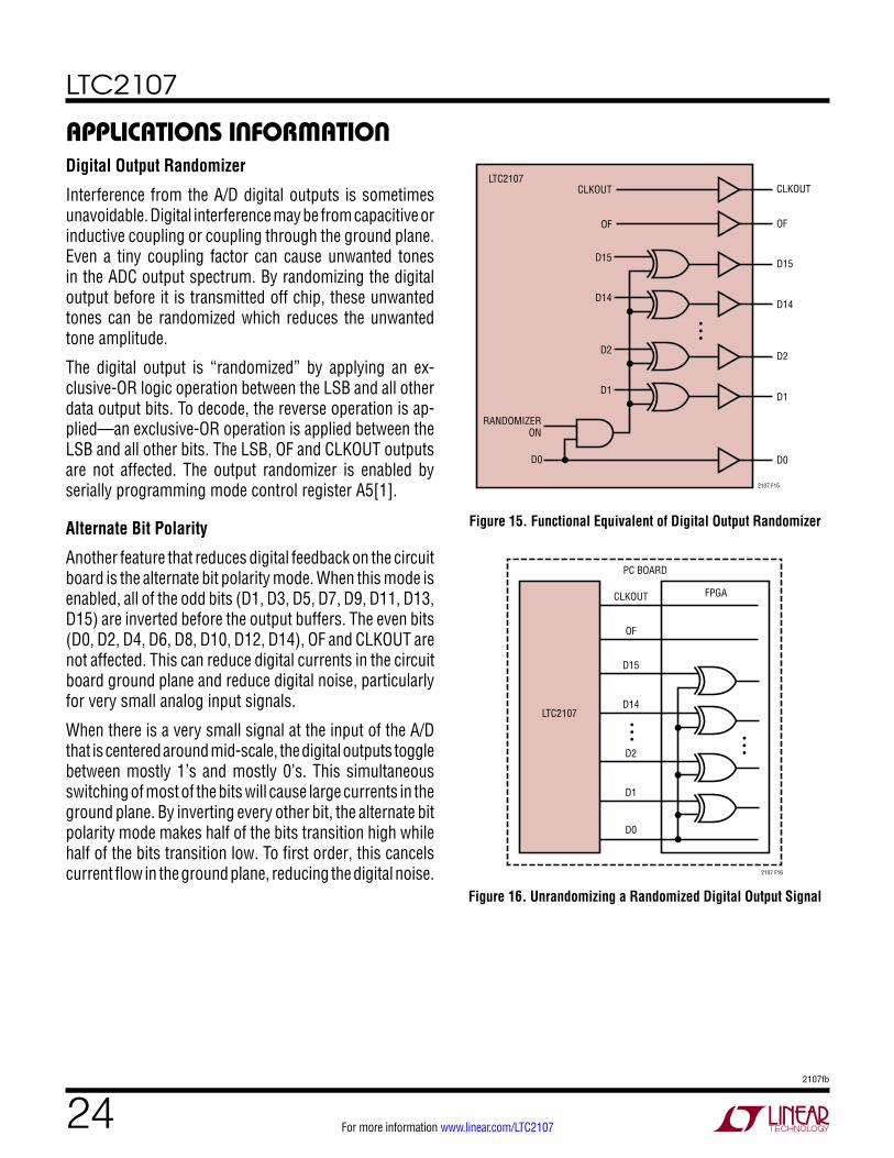
applications inFormationDigital Output Randomizer
Interference from the A/D digital outputs is sometimes unavoidable. Digital interference may be from capacitive or inductive coupling or coupling through the ground plane. Even a tiny coupling factor can cause unwanted tones in the ADC output spectrum. By randomizing the digital output before it is transmitted off chip, these unwanted tones can be randomized which reduces the unwanted tone amplitude.
The digital output is “randomized” by applying an ex-clusive-OR logic operation between the LSB and all other data output bits. To decode, the reverse operation is ap-plied—an exclusive-OR operation is applied between the LSB and all other bits. The LSB, OF and CLKOUT outputs are not affected. The output randomizer is enabled by serially programming mode control register A5[1].
Alternate Bit Polarity
Another feature that reduces digital feedback on the circuit board is the alternate bit polarity mode. When this mode is enabled, all of the odd bits (D1, D3, D5, D7, D9, D11, D13, D15) are inverted before the output buffers. The even bits (D0, D2, D4, D6, D8, D10, D12, D14), OF and CLKOUT are not affected. This can reduce digital currents in the circuit board ground plane and reduce digital noise, particularly for very small analog input signals.
When there is a very small signal at the input of the A/D that is centered around mid-scale, the digital outputs toggle between mostly 1’s and mostly 0’s. This simultaneous switching of most of the bits will cause large currents in the ground plane. By inverting every other bit, the alternate bit polarity mode makes half of the bits transition high while half of the bits transition low. To first order, this cancels current flow in the ground plane, reducing the digital noise.
Figure 15. Functional Equivalent of Digital Output Randomizer
Figure 16. Unrandomizing a Randomized Digital Output Signal
D15
OF
D15
OF
CLKOUT CLKOUTLTC2107
D14D14
D2 D2
D1
D0
2107 F15
D1
D0
RANDOMIZERON
•••
•••
•••
FPGACLKOUT
PC BOARD
OF
D15
D14
D2
D1
D0
2107 F16
LTC2107
LTC2107
252107fb
For more information www.linear.com/LTC2107
applications inFormationThe digital output is decoded at the receiver by inverting the odd bits (D1, D3, D5, D7, D9, D11, D13, D15). The alternate bit polarity mode is independent of the digital output randomizer—either, both or neither function can be on at the same time. The alternate bit polarity mode is enabled by serially programming mode control register A5[2].
Digital Output Test Patterns
To allow in-circuit testing of the digital interface to the A/D, there are several test modes that force the A/D data outputs (OF, D15-D0) to known values:
All 1s: All outputs are 1
All 0s: All outputs are 0
Alternating: Outputs change from all 1s to all 0s on alter-nating samples.
Checkerboard: Outputs change from 10101010101010101 to 01010101010101010 on alternating samples.
The digital output test patterns are enabled by serially pro-gramming mode control register A5[5:3]. When enabled, the Test Patterns override all other formatting modes: 2’s complement, randomizer, alternate-bit-polarity.
Output Disable
The digital outputs may be disabled by serially program-ming mode control register A4[2]. All digital outputs in-cluding OF and CLKOUT are disabled. The high impedance disabled state is intended for long periods of inactivity—it is too slow to multiplex a data bus between multiple con-verters at full speed.
Shutdown Mode
The A/D may be placed in shutdown mode to conserve power. In shutdown mode the entire A/D converter is powered down, resulting in 6.4mW power consumption. Shutdown mode is enabled by mode control register A1[1] (serial programming mode), or by SHDN (parallel or se-rial programming mode). The amount of time required to recover from shutdown is shown in the mid-scale settling performance plots.
DEVICE PROGRAMMING MODES
The operating modes of the LTC2107 can be programmed by either a parallel interface or a simple serial interface. The serial interface has more flexibility and can program all available modes. The parallel interface is more limited and can only program some of the more commonly used modes.
Parallel Programming Mode
To use the parallel programming mode, PAR/SER should be tied to VDD. The CS, SCK, SDI, and SHDN pins are binary logic inputs that set certain operating modes. These pins can be tied to VDD or ground, or driven by 1.8V, 2.5V, or 3.3V CMOS logic. Table 3 shows the modes set by CS, SCK, SDI and SHDN.
Table 3. Parallel Programming Mode Control BitsPIN DESCRIPTION
CS Digital Output Mode Control Bit0 = Full Rate CMOS Digital Output Mode 1 = Double Data Rate (DDR) LVDS Output Modes
SCK Programmable Gain Front-End (PGA) Control Bit0 = Front-End Gain = 1 (FS = 2.4VP-P) 1 = Front-End Gain = 1.5 (FS = 1.6VP-P)
SDI Digital Output Randomizer Control Bit0 = Digital Output Randomization Disabled 1 = Digital Output Randomization Enabled
SHDN 0 = Normal Operation 1 = ADC Power Shut Down
LTC2107
262107fb
For more information www.linear.com/LTC2107
applications inFormationSerial Programming Mode
To use the Serial Programming mode, the PAR/SER pin should be tied to ground. The CS, SCK, SDI and SDO pins become the Serial Peripheral Interface (SPI) pins that program the A/D control registers. Data is written to a register with a 16-bit serial word. Data can also be read back from a register to verify its contents.
Serial data transfer starts when CS is taken low. SCK must be low at the time of the falling edge of CS for proper operation (see the SPI Timing Diagrams). The data on the SDI pin is latched at the first 16 rising edges of SCK. Any SCK rising edges after the first 16 are ignored. The data transfer ends when CS is taken high again.
The first bit of the 16-bit input word is the R/W bit. The next 7 bits are the address of the register (A6:A0). The final 8 bits are the register data (D7:D0). If the R/W bit is low, the serial data (D7:D0) will be written to the register set by the address bits (A6:A0).
If the R/W bit is high, data in the register set by the ad-dress bits (A6:A0) will be read back on the SDO pin (see the SPI Timing Diagrams). During a read-back command the register is not updated and data on SDI is ignored.
The SDO pin is an open-drain output that pulls to ground through a 260Ω resistance. If register data is read back through SDO, an external 2k pull-up resistor is required. If serial data is only written and read-back is not needed, SDO may be left floating and no pull-up resistor is needed.
Table 4 shows a map of the mode control registers.
Software Reset
If serial programming is used, the mode control registers should be programmed as soon as possible after the power supplies turn on and are stable. The first serial command
must be a software reset which will reset all register data bits to logic 0. To perform a software reset, bit A0[7] in the reset register is written with a logic 1. After the reset is complete, bit A0[7] is automatically set back to zero. All serial control bits are set to zero after a reset.
GROUNDING AND BYPASSING
The LTC2107 requires a printed circuit board with a clean unbroken ground plane. A multilayer board with an internal ground plane is recommended. Layout for the printed circuit board should ensure that digital and analog signal lines are separated as much as possible. In particular, care should be taken not to run any digital track alongside an analog signal track or underneath the ADC.
High quality ceramic bypass capacitors should be used at the VDD, OVDD, and VCM pins. Bypass capacitors must be located as close to the pins as possible. Size 0402 ceramic capacitors are recommended for the 0.1µF, 1µF, 2.2µF and 10µF decoupling capacitors. The traces connecting the pins and bypass capacitors must be kept short and should be made as wide as possible.
The analog inputs, encode signals, and digital outputs should not be routed next to each other. Ground fill and grounded vias should be used as barriers to isolate these signals from each other.
HEAT TRANSFER
Most of the heat generated by the LTC2107 is transferred from the die through the bottom-side exposed pad and package leads onto the printed circuit board. For good electrical and thermal performance, the exposed pad must be soldered to a large grounded pad on the PC board.

LTC2107
272107fb
For more information www.linear.com/LTC2107
applications inFormationTable 4. Serial Programming Mode Register Map
REGISTER A0: RESET REGISTER (ADDRESS 00h)
D7 D6 D5 D4 D3 D2 D1 D0
RESET X X X X X X X
Bits 7 RESET Software Reset Bit 0 = Not Used
1 = Software Reset. All Mode Control Registers are reset to 00h. This bit is automatically set back to zero after the reset is complete. The Reset Register is Write Only.
Bits 6-0 Unused Bits. Read back as 0.
REGISTER A1: ADC CONTROL REGISTER (ADDRESS 01h)
D7 D6 D5 D4 D3 D2 D1 D0
X X X X PGA DITH SHDN X
Bits 7-4,0 Unused Bits. Read back as 0.Bit 3 PGA Programmable Gain Front-End Control Bit 0 = Front-End Gain of 1. Default value at start-up. 1 = Front-End Gain of 1.5Bit 2 DITH Dither Control Bit 0 = Dither Enabled. Default value at start-up. 1 = Dither DisabledBit 1 SHDN ADC Power Shut Down Control Bit 0 = Normal Operation. Default value at start-up. 1 = ADC Power Shut Down
LTC2107
282107fb
For more information www.linear.com/LTC2107
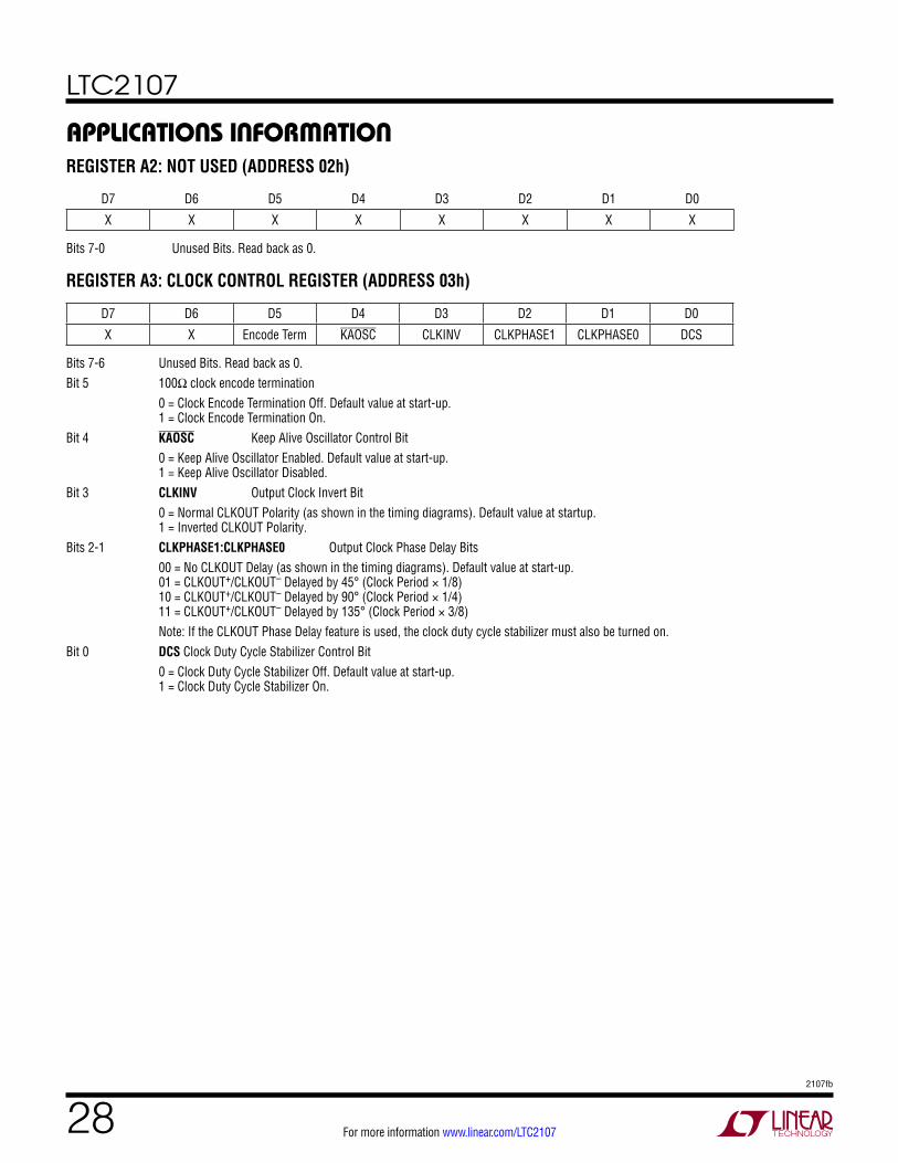
REGISTER A2: NOT USED (ADDRESS 02h)
D7 D6 D5 D4 D3 D2 D1 D0
X X X X X X X X
Bits 7-0 Unused Bits. Read back as 0.
REGISTER A3: CLOCK CONTROL REGISTER (ADDRESS 03h)
D7 D6 D5 D4 D3 D2 D1 D0
X X Encode Term KAOSC CLKINV CLKPHASE1 CLKPHASE0 DCS
Bits 7-6 Unused Bits. Read back as 0.Bit 5 100Ω clock encode termination 0 = Clock Encode Termination Off. Default value at start-up. 1 = Clock Encode Termination On.Bit 4 KAOSC Keep Alive Oscillator Control Bit 0 = Keep Alive Oscillator Enabled. Default value at start-up. 1 = Keep Alive Oscillator Disabled.Bit 3 CLKINV Output Clock Invert Bit 0 = Normal CLKOUT Polarity (as shown in the timing diagrams). Default value at startup. 1 = Inverted CLKOUT Polarity.Bits 2-1 CLKPHASE1:CLKPHASE0 Output Clock Phase Delay Bits 00 = No CLKOUT Delay (as shown in the timing diagrams). Default value at start-up. 01 = CLKOUT+/CLKOUT– Delayed by 45° (Clock Period × 1/8) 10 = CLKOUT+/CLKOUT– Delayed by 90° (Clock Period × 1/4) 11 = CLKOUT+/CLKOUT– Delayed by 135° (Clock Period × 3/8) Note: If the CLKOUT Phase Delay feature is used, the clock duty cycle stabilizer must also be turned on.Bit 0 DCS Clock Duty Cycle Stabilizer Control Bit 0 = Clock Duty Cycle Stabilizer Off. Default value at start-up. 1 = Clock Duty Cycle Stabilizer On.
applications inFormation

LTC2107
292107fb
For more information www.linear.com/LTC2107
REGISTER A4: OUTPUT MODE REGISTER (ADDRESS 04h)
D7 D6 D5 D4 D3 D2 D1 D0
X ILVDS2 ILVDS1 ILVDS0 TERMON OUTOFF X LVDS
Bit 7 Unused Bit. Read back as 0.Bits 6-4 ILVDS2:ILVDS0 LVDS Output Current Control Bits 000 = 3.5mA LVDS Output Driver Current. Default value at start-up. 001 = 4.0mA LVDS Output Driver Current. 010 = 4.5mA LVDS Output Driver Current. 011 = Not Used. 100 = 3.0mA LVDS Output Driver Current. 101 = 2.5mA LVDS Output Driver Current. 110 = 2.1mA LVDS Output Driver Current. 111 = 1.75mA LVDS Output Driver Current.Bit 3 TERMON LVDS Internal Termination Bit 0 = Internal Termination Off. Default value at start-up. 1 = Internal Termination On. LVDS output driver current is 2× the current set by ILVDS2:ILVDS0Bit 2 OUTOFF Output Disable Bit 0 = Digital Outputs are Enabled. Default value at start-up. 1 = Digital Outputs are Disabled and Have High Output Impedance.Bit 1 Unused Bit. Read back as 0.Bit 0 LVDS Digital Output Mode Control Bit 0 = Double Data Rate LVDS Output Mode. Default value at start-up. 1 = Full-Rate CMOS Output Mode.
applications inFormation
REGISTER A5: DATA FORMAT REGISTER (ADDRESS 05h)
D7 D6 D5 D4 D3 D2 D1 D0
X X OUTTEST2 OUTTEST1 OUTTEST0 ABP RAND TWOSCOMP
Bits 7-6 Unused Bits. Read back as 0.Bits 5-3 OUTTEST2:OUTTEST0 Digital Output Test Pattern Bits 000 = Digital Output Test Patterns Off. Default value at start-up. 001 = All Digital Outputs = 0. 011 = All Digital Outputs = 1. 101 = Checkerboard Output Pattern. OF, D15-D0 alternate between 10101 0101 0101 0101 and 01010 1010 1010 1010. 111 = Alternating Output Pattern. OF, D15-D0 alternate between 00000 0000 0000 0000 and 11111 1111 1111 1111. Note: Other bit combinations are not usedBit 2 ABP Alternate Bit Polarity Mode Control Bit 0 = Alternate Bit Polarity Mode Off. Default value at start-up. 1 = Alternate Bit Polarity Mode On.Bit 1 RAND Data Output Randomizer Mode Control Bit 0 = Data Output Randomizer Mode Off. Default value at start-up. 1 = Data Output Randomizer Mode On.Bits 0 TWOSCOMP Two’s Complement Mode Control Bit 0 = Offset Binary Data Format. Default value at start-up. 1 = Two’s Complement Data Format.
LTC2107
302107fb
For more information www.linear.com/LTC2107
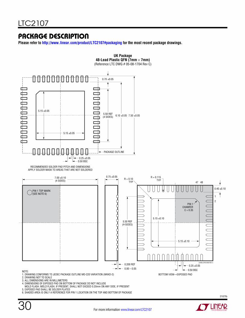
package DescriptionPlease refer to http://www.linear.com/product/LTC2107#packaging for the most recent package drawings.
7.00 ±0.10(4 SIDES)
NOTE:1. DRAWING CONFORMS TO JEDEC PACKAGE OUTLINE MO-220 VARIATION (WKKD-2)2. DRAWING NOT TO SCALE 3. ALL DIMENSIONS ARE IN MILLIMETERS4. DIMENSIONS OF EXPOSED PAD ON BOTTOM OF PACKAGE DO NOT INCLUDE MOLD FLASH. MOLD FLASH, IF PRESENT, SHALL NOT EXCEED 0.20mm ON ANY SIDE, IF PRESENT5. EXPOSED PAD SHALL BE SOLDER PLATED6. SHADED AREA IS ONLY A REFERENCE FOR PIN 1 LOCATION ON THE TOP AND BOTTOM OF PACKAGE
PIN 1 TOP MARK(SEE NOTE 6)
PIN 1CHAMFER
C = 0.35
0.40 ±0.10
4847
1
2
BOTTOM VIEW—EXPOSED PAD
5.50 REF(4-SIDES)
0.75 ±0.05 R = 0.115TYP
0.25 ±0.05
0.50 BSC
0.200 REF
0.00 – 0.05
(UK48) QFN 0406 REV C
RECOMMENDED SOLDER PAD PITCH AND DIMENSIONSAPPLY SOLDER MASK TO AREAS THAT ARE NOT SOLDERED
0.70 ±0.05
5.50 REF(4 SIDES) 6.10 ±0.05 7.50 ±0.05
0.25 ±0.050.50 BSC
PACKAGE OUTLINE
5.15 ±0.10
5.15 ±0.10
5.15 ±0.05
5.15 ±0.05
R = 0.10TYP
UK Package48-Lead Plastic QFN (7mm × 7mm)
(Reference LTC DWG # 05-08-1704 Rev C)
LTC2107
312107fb
For more information www.linear.com/LTC2107
Information furnished by Linear Technology Corporation is believed to be accurate and reliable. However, no responsibility is assumed for its use. Linear Technology Corporation makes no representa-tion that the interconnection of its circuits as described herein will not infringe on existing patent rights.
revision historyREV DATE DESCRIPTION PAGE NUMBER
A 08/15 Updated the SPI Port Timing description, diagrams and programming information 6, 8 and 26
B 12/15 Updated Figure 13 21

LTC2107
322107fb
For more information www.linear.com/LTC2107 LINEAR TECHNOLOGY CORPORATION 2014
LT 1215 REV B • PRINTED IN USALinear Technology Corporation1630 McCarthy Blvd., Milpitas, CA 95035-7417(408) 432-1900 ● FAX: (408) 434-0507 ● www.linear.com/LTC2107
relateD parts
typical application
PART NUMBER DESCRIPTION COMMENTS
High Speed ADCs
LTC2208 16-Bit 130Msps, 3.3V ADC 77.7dB SNR, 100dB SFDR, 1250mW, CMOS/LVDS Outputs, 9mm × 9mm QFN-64
LTC2209 16-Bit 160Msps, 3.3V ADC 77.1dB SNR, 100dB SFDR, 1530mW, CMOS/LVDS Outputs, 9mm × 9mm QFN-64
LTC2217 16-Bit 105Msps, 3.3V ADC 81.6dB SNR, 100dB SFDR, 1190mW, CMOS/LVDS Outputs, 9mm × 9mm QFN-64
LTC2195 16-Bit 125Msps, 1.8V Dual ADC, Ultralow Power 76.8dB SNR, 90dB SFDR, 432mW, Serial LVDS Outputs, 7mm × 8mm QFN-52
LTC2271 16-Bit 20Msps, 1.8V Dual ADC, Ultralow Power 84.1dB SNR, 99dB SFDR, 185mW, Serial LVDS Outputs, 7mm × 8mm QFN-52
Fixed Gain IF Amplifiers/ADC Drivers
LTC6430-15 High Linearity Differential RF/IF Amplifier/ADC Driver 15dB Gain, +50dBm OIP3, 3dB NF at 240MHz, 5V/160mA Supply
Baseband Differential Amplifiers
LTC6409 1.1nV/√Hz Single Supply Differential Amplifier/ADC Driver
88dB SFDR at 100MHz, AC- or DC-Coupled Inputs, 3mm × 2mm QFN-10
RF Mixers
LTC5551 300MHz to 3.5GHz Ultrahigh Dynamic Range Mixer +36dBm IIP3, 2.4dB Conversion Gain, 0dBm LO Drive, 670mW Total Power
LTC2107 Schematic (Serial Mode)
SENSE
GND
GND
VDD
VDD
VDD
GND
AIN+
AIN–
GND
VCM
GND
36
35
34
33
32
31
30
29
28
27
26
25
49
1
2
3
4
5
6
7
8
9
10
11
12
D12_13+
D12_13–
D10_11+
D10_11–
CLKOUT+
CLKOUT–
D8_9+
D8_9–
D6_7+
D6_7–
D4_5+
D4_5–
PADGND
ENC+
ENC–
GND
SHDN
SDO
OGND
OVDD
D0_1
–
D0_1
+
D2_3
–
D2_3
+
48 47 46 45 44 43 42 41 40 39 38 37
13 14 15 16 17 18 19 20 21 22 23 24
GND
GND
PAR/
SER CS SCK
SDI
OGND
OVDD OF
+
OF–
D14_
15+
D14_
15–
LTC2107
1µF
1µF
2.2µF
0.1µFVDD
10µF
1µFSENSE
AIN+
AIN–
OVDD
OVDD
2107 TA02
TO µCONTROLLEROR FPGA
DIGITALOUTPUTS
SPISIGNALS
ENC+
ENC–