ltc2057/ltc2057hv - high voltage, low noise zero … · vsdl shutdown threshold (sd – sdcom) low...
TRANSCRIPT
LTC2057/LTC2057HV
12057f
For more information www.linear.com/LTC2057
Typical applicaTion
FeaTures DescripTion
High Voltage, Low NoiseZero-Drift Operational Amplifier
The LTC®2057 is a high voltage, low noise, zero-drift op-erational amplifier that offers precision DC performance over a wide supply range of 4.75V to 36V or 4.75V to 60V for the LTC2057HV. Offset voltage and 1/f noise are suppressed, allowing this amplifier to achieve a maximum offset voltage of 4μV and a DC to 10Hz input noise volt-age of 200nVP-P (typ). The LTC2057’s self-calibrating circuitry results in low offset voltage drift with temperature, 0.015μV/°C (max), and zero-drift over time. The amplifier also features an excellent power supply rejection ratio (PSRR) of 160dB and a common mode rejection ratio (CMRR) of 150dB (typ).
The LTC2057 provides rail-to-rail output swing and an input common mode range that includes the V– rail (V– – 0.1V to V+ – 1.5V). In addition to low offset and noise, this amplifier features a 1.5MHz (typ) gain-bandwidth product and a 0.45V/μs (typ) slew rate.
Wide supply range, combined with low noise, low offset, and excellent PSRR and CMRR make the LTC2057 and LTC2057HV well suited for high dynamic-range test, measurement, and instrumentation systems.L, LT, LTC, LTM, Linear Technology, Over-The-Top, and the Linear logo are registered trademarks of Linear Technology Corporation. All other trademarks are the property of their respective owners.
Input Offset Voltage vs Supply Voltage
applicaTions
n Supply Voltage Range n 4.75V to 36V (LTC2057)
n 4.75V to 60V (LTC2057HV)n Offset Voltage: 4μV (Maximum)n Offset Voltage Drift: 0.015μV/°C
(Maximum, –40°C to 125°C)n Input Noise Voltage
n 200nVP-P, DC to 10Hz (Typ) n 11nV/√Hz, 1kHz (Typ)n Input Common Mode Range: V– – 0.1V to V+ – 1.5Vn Rail-to-Rail Outputn Unity Gain Stablen Gain Bandwidth Product: 1.5MHz (Typ)n Slew Rate: 0.45V/μs (Typ)n AVOL: 150dB (Typ)n PSRR: 160dB (Typ)n CMRR: 150dB (Typ)n Shutdown Mode
n High Resolution Data Acquisitionn Reference Bufferingn Test and Measurementn Electronic Scalesn Thermocouple Amplifiersn Strain Gaugesn Low-Side Current Sensen Automotive Monitors and Control
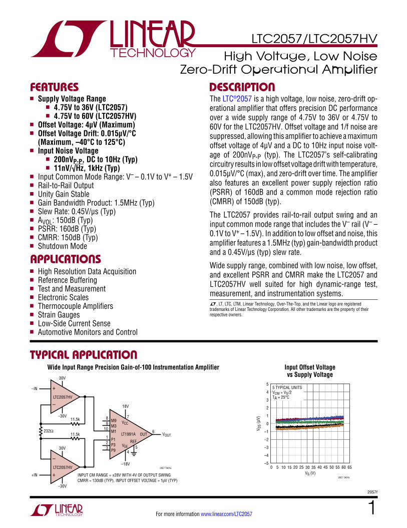
Wide Input Range Precision Gain-of-100 Instrumentation Amplifier30V
–30V
–IN
+IN
30V
11.5k
11.5k
–30V
2057 TA01a
LTC2057HV
LTC2057HV
M9M3M1
INPUT CM RANGE = ±28V WITH 4V OF OUTPUT SWINGCMRR = 130dB (TYP), INPUT OFFSET VOLTAGE = 1µV (TYP)
+
–
–
+
89
10
P1P3P9
LT1991A
18V
–18V
REF
OUT6
54
7
VOUT
VCC
VEE
232Ω123
VS (V)0
–5
–4
–3
–2
–1V OS
(µV)
0
1
5
3
4
2
10 20 30 40 505 15 25 35 45 55 6560
2057 TA01b
5 TYPICAL UNITSVCM = VS/2TA = 25°C
LTC2057/LTC2057HV
22057f
For more information www.linear.com/LTC2057
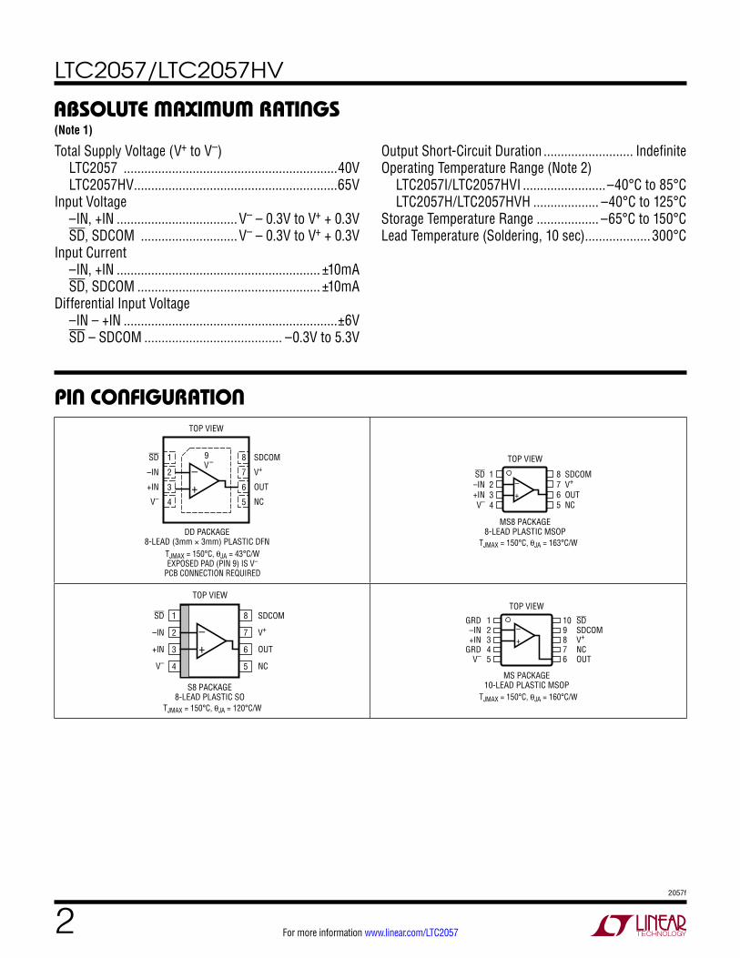
absoluTe MaxiMuM raTings
Total Supply Voltage (V+ to V–) LTC2057 ..............................................................40V LTC2057HV ...........................................................65V
Input Voltage –IN, +IN ...................................V– – 0.3V to V+ + 0.3V SD, SDCOM ............................V– – 0.3V to V+ + 0.3V
Input Current –IN, +IN ........................................................... ±10mA SD, SDCOM ..................................................... ±10mA
Differential Input Voltage –IN – +IN ..............................................................±6V SD – SDCOM ........................................ –0.3V to 5.3V
TOP VIEW
DD PACKAGE8-LEAD (3mm × 3mm) PLASTIC DFN
5
6
7
8
4
3
2
1SD
–IN
+IN
V–
SDCOM
V+
OUT
NC
–+
9 V–
TJMAX = 150°C, θJA = 43°C/W EXPOSED PAD (PIN 9) IS V–
PCB CONNECTION REQUIRED
1234
SD–IN+INV–
8765
SDCOMV+
OUTNC
TOP VIEW
MS8 PACKAGE8-LEAD PLASTIC MSOP
–+
TJMAX = 150°C, θJA = 163°C/W
1
2
3
4
8
7
6
5
TOP VIEW
SDCOM
V+
OUT
NC
SD
–IN
+IN
V–
S8 PACKAGE8-LEAD PLASTIC SO
–+
TJMAX = 150°C, θJA = 120°C/W
12345
GRD–IN+IN
GRDV–
109876
SDSDCOMV+
NCOUT
TOP VIEW
MS PACKAGE10-LEAD PLASTIC MSOP
–+
TJMAX = 150°C, θJA = 160°C/W
pin conFiguraTion
Output Short-Circuit Duration .......................... IndefiniteOperating Temperature Range (Note 2)
LTC2057I/LTC2057HVI ........................–40°C to 85°C LTC2057H/LTC2057HVH ................... –40°C to 125°C
Storage Temperature Range .................. –65°C to 150°CLead Temperature (Soldering, 10 sec) ................... 300°C
(Note 1)
LTC2057/LTC2057HV
32057f
For more information www.linear.com/LTC2057
orDer inForMaTionLEAD FREE FINISH TAPE AND REEL PART MARKING* PACKAGE DESCRIPTION TEMPERATURE RANGE
LTC2057IDD#PBF LTC2057IDD#TRPBF LGCZ 8-Lead Plastic DFN (3mm × 3mm) –40°C to 85°C
LTC2057HVIDD#PBF LTC2057HVIDD#TRPBF LGDB 8-Lead Plastic DFN (3mm × 3mm) –40°C to 85°C
LTC2057HDD#PBF LTC2057HDD#TRPBF LGCZ 8-Lead Plastic DFN (3mm × 3mm) –40°C to 125°C
LTC2057HVHDD#PBF LTC2057HVHDD#TRPBF LGDB 8-Lead Plastic DFN (3mm × 3mm) –40°C to 125°C
LTC2057IMS8#PBF LTC2057IMS8#TRPBF LTFGK 8-Lead Plastic MSOP –40°C to 85°C
LTC2057HVIMS8#PBF LTC2057HVIMS8#TRPBF LTGDC 8-Lead Plastic MSOP –40°C to 85°C
LTC2057HMS8#PBF LTC2057HMS8#TRPBF LTFGK 8-Lead Plastic MSOP –40°C to 125°C
LTC2057HVHMS8#PBF LTC2057HVHMS8#TRPBF LTGDC 8-Lead Plastic MSOP –40°C to 125°C
LTC2057IMS#PBF LTC2057IMS#TRPBF LTGCX 10-Lead Plastic MSOP –40°C to 85°C
LTC2057HVIMS#PBF LTC2057HVIMS#TRPBF LTGCY 10-Lead Plastic MSOP –40°C to 85°C
LTC2057HMS#PBF LTC2057HMS#TRPBF LTGCX 10-Lead Plastic MSOP –40°C to 125°C
LTC2057HVHMS#PBF LTC2057HVHMS#TRPBF LTGCY 10-Lead Plastic MSOP –40°C to 125°C
LTC2057IS8#PBF LTC2057IS8#TRPBF 2057 8-Lead Plastic Small Outline –40°C to 85°C
LTC2057HVIS8#PBF LTC2057HVIS8#TRPBF 2057HV 8-Lead Plastic Small Outline –40°C to 85°C
LTC2057HS8#PBF LTC2057HS8#TRPBF 2057 8-Lead Plastic Small Outline –40°C to 125°C
LTC2057HVHS8#PBF LTC2057HVHS8#TRPBF 2057HV 8-Lead Plastic Small Outline –40°C to 125°C
Consult LTC Marketing for parts specified with wider operating temperature ranges. *The temperature grade is identified by a label on the shipping container. Consult LTC Marketing for information on non-standard lead based finish parts.For more information on lead free part marking, go to: http://www.linear.com/leadfree/ For more information on tape and reel specifications, go to: http://www.linear.com/tapeandreel/
LTC2057/LTC2057HV
42057f
For more information www.linear.com/LTC2057
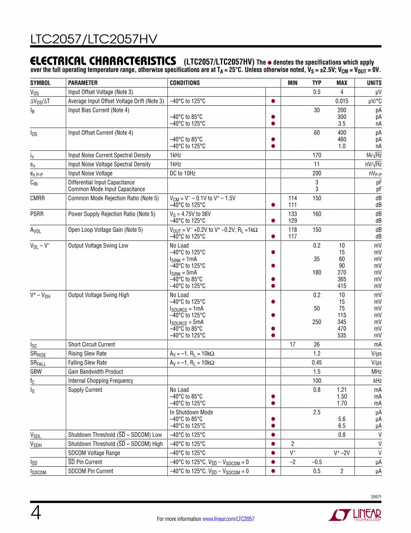
(LTC2057/LTC2057HV) The l denotes the specifications which apply over the full operating temperature range, otherwise specifications are at TA = 25°C. Unless otherwise noted, VS = ±2.5V; VCM = VOUT = 0V.elecTrical characTerisTics
SYMBOL PARAMETER CONDITIONS MIN TYP MAX UNITSVOS Input Offset Voltage (Note 3) 0.5 4 μV∆VOS/∆T Average Input Offset Voltage Drift (Note 3) –40°C to 125°C l 0.015 μV/°CIB Input Bias Current (Note 4)
–40°C to 85°C –40°C to 125°C
l
l
30 200 300 3.5
pA pA nA
IOS Input Offset Current (Note 4) –40°C to 85°C –40°C to 125°C
l
l
60 400 460 1.0
pA pA nA
in Input Noise Current Spectral Density 1kHz 170 fA/√Hzen Input Noise Voltage Spectral Density 1kHz 11 nV/√Hzen P-P Input Noise Voltage DC to 10Hz 200 nVP-P
CIN Differential Input Capacitance Common Mode Input Capacitance
3 3
pF pF
CMRR Common Mode Rejection Ratio (Note 5) VCM = V– – 0.1V to V+ – 1.5V –40°C to 125°C
l
114 111
150 dB dB
PSRR Power Supply Rejection Ratio (Note 5) VS = 4.75V to 36V –40°C to 125°C
l
133 129
160 dB dB
AVOL Open Loop Voltage Gain (Note 5) VOUT = V– +0.2V to V+ –0.2V, RL =1kΩ –40°C to 125°C
l
118 117
150 dB dB
VOL – V– Output Voltage Swing Low No Load –40°C to 125°C ISINK = 1mA –40°C to 125°C ISINK = 5mA –40°C to 85°C –40°C to 125°C
l
l
l
l
0.2
35
180
10 15 60 90
270 365 415
mV mV mV mV mV mV mV
V+ – VOH Output Voltage Swing High No Load –40°C to 125°C ISOURCE = 1mA –40°C to 125°C ISOURCE = 5mA –40°C to 85°C –40°C to 125°C
l
l
l
l
0.2
50
250
10 15 75
115 345 470 535
mV mV mV mV mV mV mV
ISC Short Circuit Current 17 26 mASRRISE Rising Slew Rate AV = –1, RL = 10kΩ 1.2 V/μsSRFALL Falling Slew Rate AV = –1, RL = 10kΩ 0.45 V/μsGBW Gain Bandwidth Product 1.5 MHzfC Internal Chopping Frequency 100 kHzIS Supply Current No Load
–40°C to 85°C –40°C to 125°C
l
l
0.8
1.21 1.50 1.70
mA mA mA
In Shutdown Mode –40°C to 85°C –40°C to 125°C
l
l
2.5 5.6 6.5
μA μA μA
VSDL Shutdown Threshold (SD – SDCOM) Low –40°C to 125°C l 0.8 VVSDH Shutdown Threshold (SD – SDCOM) High –40°C to 125°C l 2 V
SDCOM Voltage Range –40°C to 125°C l V– V+ –2V VISD SD Pin Current –40°C to 125°C, VSD – VSDCOM = 0 l –2 –0.5 μAISDCOM SDCOM Pin Current –40°C to 125°C, VSD – VSDCOM = 0 l 0.5 2 μA
LTC2057/LTC2057HV
52057f
For more information www.linear.com/LTC2057
(LTC2057/LTC2057HV) The l denotes the specifications which apply over the full operating temperature range, otherwise specifications are at TA = 25°C. Unless otherwise noted, VS = ±15V; VCM = VOUT = 0V.elecTrical characTerisTics
SYMBOL PARAMETER CONDITIONS MIN TYP MAX UNITSVOS Input Offset Voltage (Note 3) 0.5 4.5 μV∆VOS/∆T Average Input Offset Voltage Drift (Note 3) –40°C to 125°C l 0.015 μV/°CIB Input Bias Current (Note 4)
–40°C to 85°C –40°C to 125°C
l
l
30 200 360 6.0
pA pA nA
IOS Input Offset Current (Note 4) –40°C to 85°C –40°C to 125°C
l
l
60 400 480 1.5
pA pA nA
in Input Noise Current Spectral Density 1kHz 150 fA/√Hzen Input Noise Voltage Spectral Density 1kHz 12 nV/√Hzen P-P Input Noise Voltage DC to 10Hz 210 nVP-P
CIN Differential Input Capacitance Common Mode Input Capacitance
3 3
pF pF
CMRR Common Mode Rejection Ratio (Note 5) VCM = V– – 0.1V to V+ – 1.5V –40°C to 125°C
l
128 126
150 dB dB
PSRR Power Supply Rejection Ratio (Note 5) VS = 4.75V to 36V –40°C to 125°C
l
133 129
160 dB dB
AVOL Open Loop Voltage Gain (Note 5) VOUT = V– +0.25V to V+ –0.25V, RL =10kΩ –40°C to 125°C
l
130 128
150 dB dB
VOL – V– Output Voltage Swing Low No Load –40°C to 125°C ISINK = 1mA –40°C to 125°C ISINK = 5mA –40°C to 85°C –40°C to 125°C
l
l
l
l
2
35
175
12 45 60
100 255 360 435
mV mV mV mV mV mV mV
V+ – VOH Output Voltage Swing High No Load –40°C to 125°C ISOURCE = 1mA –40°C to 125°C ISOURCE = 5mA –40°C to 85°C –40°C to 125°C
l
l
l
l
3
50
235
15 45 75
125 335 465 560
mV mV mV mV mV mV mV
ISC Short Circuit Current 19 30 mASRRISE Rising Slew Rate AV = –1, RL = 10kΩ 1.3 V/μsSRFALL Falling Slew Rate AV = –1, RL = 10kΩ 0.45 V/μsGBW Gain Bandwidth Product 1.5 MHzfC Internal Chopping Frequency 100 kHzIS Supply Current No Load
–40°C to 85°C –40°C to 125°C
l
l
0.88
1.35 1.65 1.83
mA mA mA
In Shutdown Mode –40°C to 85°C –40°C to 125°C
l
l
3 8 9
μA μA μA
VSDL Shutdown Threshold (SD – SDCOM) Low –40°C to 125°C l 0.8 VVSDH Shutdown Threshold (SD – SDCOM) High –40°C to 125°C l 2 V
SDCOM Voltage Range –40°C to 125°C l V– V+ –2V VISD SD Pin Current –40°C to 125°C, VSD – VSDCOM = 0 l –2.0 –0.5 µAISDCOM SDCOM Pin Current –40°C to 125°C, VSD – VSDCOM = 0 l 0.5 2 µA
LTC2057/LTC2057HV
62057f
For more information www.linear.com/LTC2057
(LTC2057HV) The l denotes the specifications which apply over the full operating temperature range, otherwise specifications are at TA = 25°C. Unless otherwise noted, VS = ±30V; VCM = VOUT = 0V.elecTrical characTerisTicsSYMBOL PARAMETER CONDITIONS MIN TYP MAX UNITSVOS Input Offset Voltage (Note 3) 0.5 5 μV∆VOS/∆T Average Input Offset Voltage Drift (Note 3) –40°C to 125°C l 0.025 μV/°CIB Input Bias Current (Note 4)
–40°C to 85°C –40°C to 125°C
l
l
30 200 455 11
pA pA nA
IOS Input Offset Current (Note 4) –40°C to 85°C –40°C to 125°C
l
l
60 400 500 3
pA pA nA
in Input Noise Current Spectral Density 1kHz 130 fA/√Hzen Input Noise Voltage Spectral Density 1kHz 13 nV/√Hzen P-P Input Noise Voltage DC to 10Hz 220 nVP-P
CIN Differential Input Capacitance Common Mode Input Capacitance
3 3
pF pF
CMRR Common Mode Rejection Ratio (Note 5) VCM = V– – 0.1V to V+ – 1.5V –40°C to 125°C
l
133 131
150 dB dB
PSRR Power Supply Rejection Ratio (Note 5) VS = 4.75V to 60V –40°C to 125°C
l
138 136
160 dB dB
AVOL Open Loop Voltage Gain (Note 5) VOUT = V– +0.25V to V+ – 0.25V, RL = 10kΩ –40°C to 125°C
l
135 130
150 dB dB
VOL – V– Output Voltage Swing Low No Load –40°C to 125°C ISINK = 1mA –40°C to 125°C ISINK = 5mA –40°C to 85°C –40°C to 125°C
l
l
l
l
3
35
175
15 45 60
105 260 370 445
mV mV mV mV mV mV mV
V+ – VOH Output Voltage Swing High No Load –40°C to 125°C ISOURCE = 1mA –40°C to 125°C ISOURCE = 5mA –40°C to 85°C –40°C to 125°C
l
l
l
l
3
50
235
15 45 75
130 335 475 575
mV mV mV mV mV mV mV
ISC Short Circuit Current 19 30 mASRRISE Rising Slew Rate AV = –1, RL = 10kΩ 1.3 V/μsSRFALL Falling Slew Rate AV = –1, RL = 10kΩ 0.45 V/μsGBW Gain Bandwidth Product 1.5 MHzfC Internal Chopping Frequency 100 kHzIS Supply Current No Load
–40°C to 85°C –40°C to 125°C
l
l
0.90
1.40 1.73 1.92
mA mA mA
In Shutdown Mode –40°C to 85°C –40°C to 125°C
l
l
3 9
11
μA μA μA
VSDL Shutdown Threshold (SD – SDCOM) Low –40°C to 125°C l 0.8 V
VSDH Shutdown Threshold (SD – SDCOM) High –40°C to 125°C l 2 V
SDCOM Voltage Range –40°C to 125°C l V– V+ –2V V
ISD SD Pin Current –40°C to 125°C, VSD – VSDCOM = 0 l –2 –0.5 µA
ISDCOM SDCOM Pin Current –40°C to 125°C, VSD – VSDCOM = 0 l 0.5 2 µA
LTC2057/LTC2057HV
72057f
For more information www.linear.com/LTC2057
Note 1: Stresses beyond those listed under Absolute Maximum Ratings may cause permanent damage to the device. Exposure to any Absolute Maximum Rating condition for extended periods may affect device reliability and lifetime.Note 2: The LTC2057I/LTC2057HVI are guaranteed to meet specified performance from –40°C to 85°C. The LTC2057H/LTC2057HVH are guaranteed to meet specified performance from –40°C to 125°C.Note 3: These parameters are guaranteed by design. Thermocouple effects preclude measurements of these voltage levels during automated testing. VOS is measured to a limit determined by test equipment capability.
Note 4: These specifications are limited by automated test system capability. Leakage currents and thermocouple effects reduce test accuracy. For tighter specifications, please contact LTC Marketing.Note 5: Minimum specifications for these parameters are limited by the capabilities of the automated test system, which has an accuracy of approximately 10µV for VOS measurements. For reference, 10µV/60V is 136dB, 10µV/30V is 130dB, and 10µV/5V is 114dB.
elecTrical characTerisTics
LTC2057/LTC2057HV
82057f
For more information www.linear.com/LTC2057
Input Offset Voltage Distribution Input Offset Voltage Distribution Input Offset Voltage Distribution
Input Offset Voltage Drift Distribution
Input Offset Voltage Drift Distribution
Input Offset Voltage Drift Distribution
Typical perForMance characTerisTics
Input Offset Voltage vs Input Common Mode Voltage
Input Offset Voltage vs Input Common Mode Voltage
Input Offset Voltage vs Input Common Mode Voltage
VCM (V)–1
–5
–4
–3
–2
–1V OS
(µV)
0
1
5
3
4
2
0 1 2 3 4 5
2057 G07
5 TYPICAL UNITSVS = 5VTA = 25°C
VCM (V)0
–5
–4
–3
–2
–1V OS
(µV)
0
1
5
3
4
2
5 10 15 20 25 30
2057 G08
5 TYPICAL UNITSVS = 30VTA = 25°C
VCM (V)0
–5
–4
–3
–2
–1V OS
(µV)
0
1
5
3
4
2
10 20 30 40 50 60
2057 G09
5 TYPICAL UNITSVS = 60VTA = 25°C
VOS (µV)–3 –2.5
0
5
10NUM
BER
OF A
MPL
IFIE
RS
15
20
40
30
35
25
–2 –1.5 –1 –0.5 0 0.5 1 1.5 2 2.5 3
2057 G01
160 TYPICAL UNITSVS = ±2.5V
µ = –0.441 µVσ = 0.452µV
VOS (µV)–3 –2.5
0
5
10
NUM
BER
OF A
MPL
IFIE
RS15
20
35
30
25
–2 –1.5 –1 –0.5 0 0.5 1 1.5 2 2.5 3
2057 G02
160 TYPICAL UNITSVS = ±15V
µ = –0.432 µVσ = 0.525µV
VOS (µV)–3 –2.5
0
5
10
NUM
BER
OF A
MPL
IFIE
RS
15
20
35
30
25
–2 –1.5 –1 –0.5 0 0.5 1 1.5 2 2.5 3
2057 G03
160 TYPICAL UNITSVS = ±30V
µ = –0.507 µVσ = 0.548µV
VOS TC (nV/°C)1
0
10
20NUM
BER
OF A
MPL
IFIE
RS
30
40
90
60
70
80
50
3 5 7 9 11 13 15 17 19
2057 G04
160 TYPICAL UNITSVS = ±2.5V
TA = –40°C TO 125°Cµ = 1.16nV/°Cσ = 0.97nV/°C
VOS TC (nV/°C)1
0
10
20NUM
BER
OF A
MPL
IFIE
RS
30
40
80
60
70
50
3 5 7 9 11 13 15 17 19
2057 G05
160 TYPICAL UNITSVS = ±15V
TA = –40°C TO 125°Cµ = 1.29nV/°Cσ = 1.14nV/°C
VOS TC (nV/°C)1
0
10
20NUM
BER
OF A
MPL
IFIE
RS
30
40
90
80
60
70
50
3 5 7 9 11 13 15 17 19
2057 G06
160 TYPICAL UNITSVS = ±30V
TA = –40°C TO 125°Cµ = 1.32nV/°Cσ = 1.26nV/°C
LTC2057/LTC2057HV
92057f
For more information www.linear.com/LTC2057
Typical perForMance characTerisTics
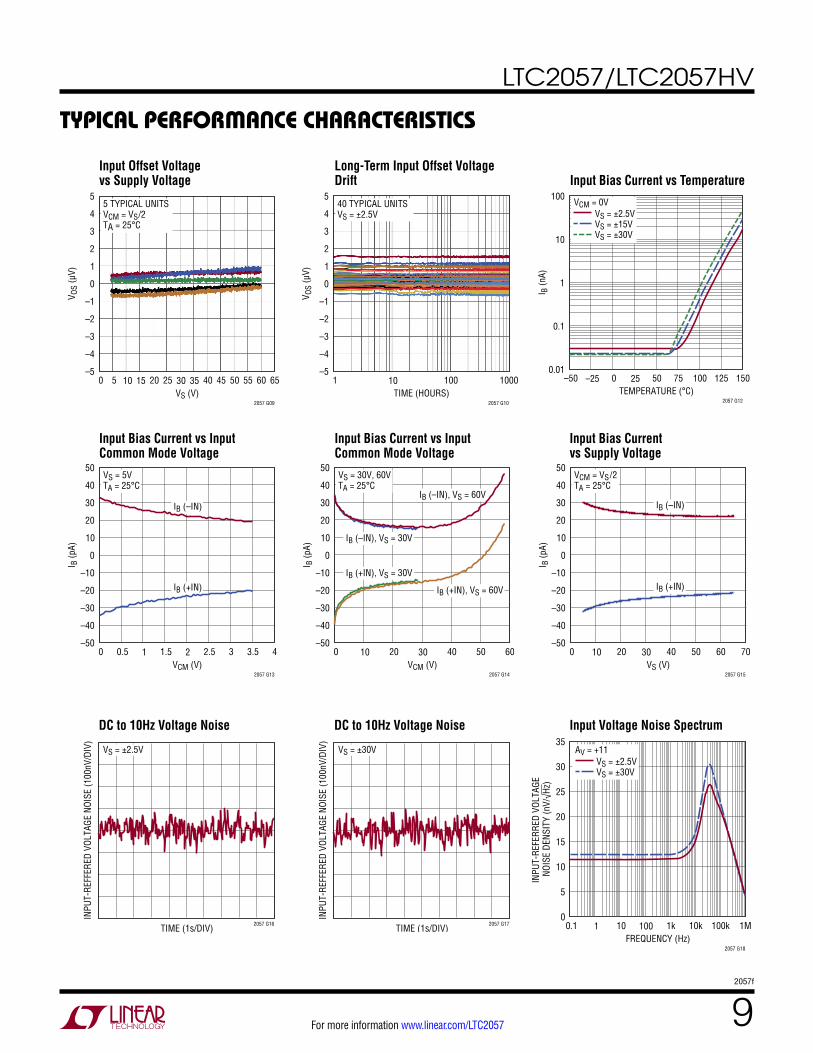
DC to 10Hz Voltage Noise DC to 10Hz Voltage Noise Input Voltage Noise Spectrum
Input Offset Voltage vs Supply Voltage
Long-Term Input Offset Voltage Drift
Input Bias Current vs Supply Voltage
Input Bias Current vs Input Common Mode Voltage
Input Bias Current vs Input Common Mode Voltage
Input Bias Current vs Temperature
VS (V)0
–5
–4
–3
–2
–1V OS
(µV)
0
1
5
3
4
2
10 20 30 40 505 15 25 35 45 55 6560
2057 G09
5 TYPICAL UNITSVCM = VS/2TA = 25°C
TEMPERATURE (°C)–50
0.01
0.1
1
10
I B (n
A)
100
–25 0 25 50 75 100 125 150
2057 G12
VS = ±2.5VVS = ±15VVS = ±30V
VCM = 0V
VCM (V)0
–50
–40
–30
–20
–10
I B (p
A)
0
10
50
30
40
20
1 1.50.5 2 2.5 3 43.5
2057 G13
IB (–IN)
IB (+IN)
VS = 5VTA = 25°C
VCM (V)0
–50
–40
–30
–20
–10
I B (p
A)
0
10
50
30
40
20
10 20 30 40 50 60
2057 G14
VS = 30V, 60VTA = 25°C
IB (–IN), VS = 60V
IB (+IN), VS = 60V
IB (–IN), VS = 30V
IB (+IN), VS = 30V
VS (V)0
–50
–40
–30
–20
–10
I B (p
A)0
10
50
30
40
20
10 20 30 40 50 7060
2057 G15
IB (–IN)
IB (+IN)
VCM = VS/2TA = 25°C
TIME (HOURS)1
–5
–4
–3
–2
–1V OS
(µV)
0
1
5
3
4
2
10 100 1000
2057 G10
40 TYPICAL UNITSVS = ±2.5V
TIME (1s/DIV)
INPU
T-RE
FFER
ED V
OLTA
GE N
OISE
(100
nV/D
IV)
2057 G16
VS = ±2.5V
TIME (1s/DIV)
INPU
T-RE
FFER
ED V
OLTA
GE N
OISE
(100
nV/D
IV)
2057 G17
VS = ±30V
FREQUENCY (Hz)0.1
0
5
10
15
20
30
25
INPU
T-RE
FERR
ED V
OLTA
GE
NOIS
E DE
NSIT
Y (n
V/√H
z)
35
1 10 100 1k 10k 100k 1M
2057 G18
VS = ±2.5VVS = ±30V
AV = +11
LTC2057/LTC2057HV
102057f
For more information www.linear.com/LTC2057
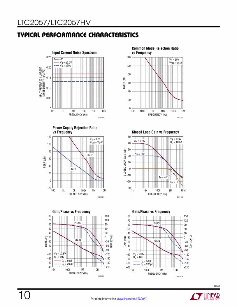
Typical perForMance characTerisTics
Input Current Noise SpectrumCommon Mode Rejection Ratio vs Frequency
Power Supply Rejection Ratio vs Frequency Closed Loop Gain vs Frequency
Gain/Phase vs Frequency Gain/Phase vs Frequency
FREQUENCY (Hz)0.1
0
0.05
0.10
0.20
0.15
INPU
T-RE
FERR
ED C
URRE
NTNO
ISE
DENS
ITY
(pA/
√Hz)
0.25
1 10 100 1k 10k
2057 G19
VS = ±2.5VVS = ±30V
AV = +11
FREQUENCY (Hz)100
0
20
60
40
100
80
CMRR
(dB)
120
1000 1k 10k 100k 1M
2057 G20
VS = 30VVCM = VS/2
FREQUENCY (Hz)10k
–40
–20
0
60
40
20
GAIN
(dB)
PHASE (dB)
80
–30
–10
50
30
10
70
–210
–150
–90
90
30
–30
150
–180
–120
60
0
–60
120
100k 1M 10M
2057 G23
VS = ±2.5VRL = 1kΩ
CL = 50pFCL = 200pF
PHASE
GAIN
FREQUENCY (Hz)100
–20
0
20
60
40
100
80
PSRR
(dB)
120
1k 10k 100k 1M 10M
2057 G21
VS = 30VVCM = VS/2
+PSRR
–PSRR
FREQUENCY (Hz)10k
–40
–20
0
60
40
20
GAIN
(dB)
PHASE (dB)
80
–30
–10
50
30
10
70
–210
–150
–90
90
30
–30
150
–180
–120
60
0
–60
120
100k 1M 10M
2057 G24
VS = ±30VRL = 1kΩ
CL = 50pFCL = 200pF
PHASE
GAIN
FREQUENCY (Hz)1k
–30
–20
–10
20
10
0
40
30
CLOS
ED L
OOP
GAIN
(dB)
50
10k 100k 1M 10M
2057 G22
VS = ±15VRL = 10kΩ
AV = +1
AV = +10
AV = +100
AV = –1
LTC2057/LTC2057HV
112057f
For more information www.linear.com/LTC2057
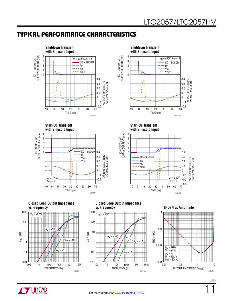
Typical perForMance characTerisTics
Shutdown Transient with Sinusoid Input
Start-Up Transient with Sinusoid Input
Shutdown Transient with Sinusoid Input
TIME (µs)–10
3
1
SD –
SDC
OM (V
)SU
PPLY
CUR
RENT
(mA)
INPUT VOLTAGE (V)OUTPUT VOLTAGE (V)
4
2
0
–0.2
0
0.1
0.2
0.3
0.4
–0.1
0 10 3020 40 50
2057 G26
VS = ±30V, AV = +1
SD – SDCOMISSVINVOUT
Start-Up Transient with Sinusoid Input
Closed Loop Output Impedance vs Frequency
Closed Loop Output Impedance vs Frequency
FREQUENCY (Hz)100
0.01
0.1
100
10
1Z OUT
(Ω)
1000
1k 10k 100k 1M 10M
2057 G29
AV = +100
AV = +1
VS = ±2.5V
AV = +10
FREQUENCY (Hz)100
0.01
0.1
100
10
1Z OUT
(Ω)
1000
1k 10k 100k 1M 10M
2057 G30
AV = +1
AV = +100
AV = +10
VS = ±30V
THD+N vs Amplitude
OUTPUT AMPLITUDE (VRMS)0.01
0.0001
0.01
0.001
THD+
N (%
)
0.1
0.1 1 10
2057 G31
fIN = 1kHzVS = ±15VAV = +1RL = 10kΩBW = 80kHz
TIME (µs)–10
3
1
SD –
SDC
OM (V
)SU
PPLY
CUR
RENT
(mA)
INPUT VOLTAGE (V)OUTPUT VOLTAGE (V)
4
2
0
–0.2
0
0.2
0.4
–0.1
0.1
0.3
0 10 3020 40 50
2057 G25
SD – SDCOMISSVINVOUT
VS = ±2.5V, AV = +1
TIME (µs)–10
3
1
SD –
SDC
OM (V
)SU
PPLY
CUR
RENT
(mA)
INPUT VOLTAGE (V)OUTPUT VOLTAGE (V)
4
2
0
–0.3
–0.1
0.1
0.3
–0.2
0.1
0.4
0.2
0 10 3020 40 50 60 70
2057 G27
SD – SDCOMISSVINVOUT
VS = ±2.5VAV = +1
TIME (µs)–10
3
1
SD –
SDC
OM (V
)SU
PPLY
CUR
RENT
(mA)
INPUT VOLTAGE (V)OUTPUT VOLTAGE (V)
4
2
0
–0.3
–0.1
0.1
0.3
–0.2
0
0.4
0.2
0 10 3020 40 7050 60
2057 G28
VS = ±30VAV = +1
SD – SDCOMISSVINVOUT
LTC2057/LTC2057HV
122057f
For more information www.linear.com/LTC2057
Typical perForMance characTerisTics
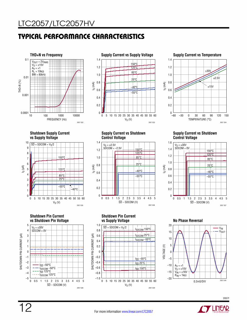
THD+N vs Frequency Supply Current vs Supply Voltage Supply Current vs Temperature
Shutdown Supply Current vs Supply Voltage
VS (V)0
0
2
1
4
3
6
5
7
9
8
I S (µ
A)
10
5 10 15 20 25 30 35 45 50 5540 60
2057 G35
–55°C–40°C
25°C85°C
125°C
150°C
SD = SDCOM = VS/2
Supply Current vs Shutdown Control Voltage
Supply Current vs Shutdown Control Voltage
SD – SDCOM (V)0
0
0.2
0.4
0.6
0.8
1.2
1.0I S
(mA)
1.6
1.4
0.5 1 1.5 2 2.5 3 3.5 4.54 5
2057 G37
–40°C
–55°C
25°C
85°C
125°C150°C
VS = ±30VSDCOM = 0V
Shutdown Pin Current vs Shutdown Pin Voltage
SD – SDCOM (V)0
–5
–3
–4
–2
–1
0
2
1
3
SHUT
DOW
N PI
N CU
RREN
T (µ
A)
5
4
0.5 1 1.5 2 2.5 3 3.5 4.54 5
2057 G38
VS = ±30VSDCOM = 0V
ISD –50°CISDCOM –50°CISD 125°CISDCOM 125°C
Shutdown Pin Current vs Supply Voltage
VS (V)0
–1.0
–0.8
–0.6
–0.4
–0.2
0.2
0
SHUT
DOW
N PI
N CU
RREN
T (µ
A)
1.0
0.4
0.6
0.8
5 10 15 20 25 30 35 4540 5550 60
2057 G39
ISDCOM –55°CISDCOM 25°C
ISDCOM 150°C
ISD –55°C
SD = SDCOM = VS/2
ISD 25°C
ISD 150°C
No Phase Reversal
VS (V)0
0
0.4
0.2
0.8
0.6
1.2
1.0
I S (m
A)
1.4
5 10 15 20 25 30 35 45 50 5540 60
2057 G33
–55°C
–40°C
25°C
85°C
125°C150°C
TEMPERATURE (°C)–60
0
0.4
0.2
0.8
0.6
1.2
1.0
I S (m
A)
1.4
–30 0 30 60 90 120 150
2057 G34
±30V
±2.5V
±15V
FREQUENCY (Hz)10
0.0001
0.01
0.001
THD+
N (%
)
0.1
100 1000 10000
2057 G32
VOUT = 2VRMSVS = ±15VAV = +1RL = 10kΩBW = 80kHz
SD – SDCOM (V)0
0
0.2
0.4
0.6
0.8
1.2
1.0
I S (m
A)
1.4
0.5 1 1.5 2 2.5 3 3.5 4.54 5
2057 G36
–40°C
–55°C
25°C
85°C
125°C150°C
VS = ±2.5VSDCOM = –2.5V
0.2mS/DIV–20
–15
–10
–5
5
0
VOLT
AGE
(V)
20
10
15
2057 G40
AV = +1VS = ±15VVIN = ±16VRIN = 1kΩ
VINVOUT
LTC2057/LTC2057HV
132057f
For more information www.linear.com/LTC2057
Typical perForMance characTerisTics
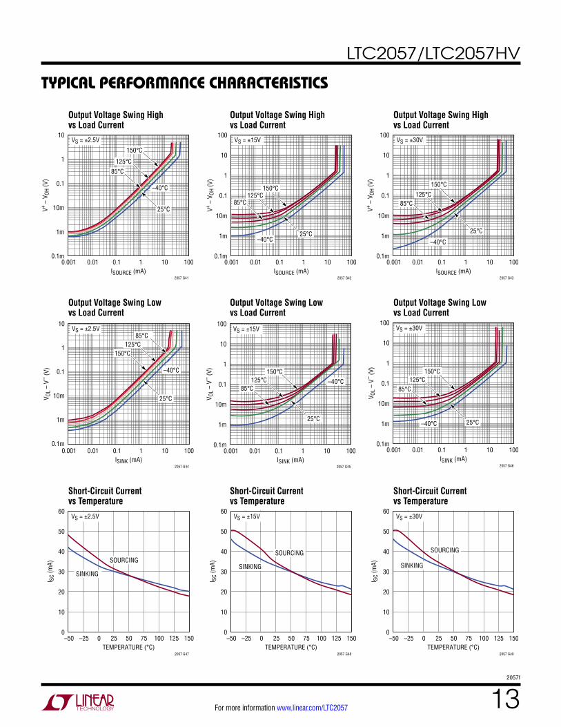
Output Voltage Swing High vs Load Current
Output Voltage Swing High vs Load Current
Output Voltage Swing High vs Load Current
Output Voltage Swing Low vs Load Current
Output Voltage Swing Low vs Load Current
Output Voltage Swing Low vs Load Current
Short-Circuit Current vs Temperature
Short-Circuit Current vs Temperature
Short-Circuit Current vs Temperature
ISOURCE (mA)0.001
0.1m
1m
0.1
10mV+ – V
OH (V
)
10
1
0.01 0.1 1 10 100
2057 G41
–40°C
25°C
VS = ±2.5V
85°C
125°C
150°C
ISOURCE (mA)0.001
0.1m
1m
0.1
10mV+ –
VOH
(V)
100
10
1
0.01 0.1 1 10 100
2057 G42
–40°C
VS = ±15V
85°C125°C
25°C
150°C
ISINK (mA)0.001
0.1m
1m
0.1
10mV OL
– V
– (V)
10
1
0.01 0.1 1 10 100
2057 G44
–40°C
VS = ±2.5V
25°C
150°C
85°C125°C
ISINK (mA)0.001
0.1m
1m
0.1
10m
V OL
– V
– (V)
100
10
1
0.01 0.1 1 10 100
2057 G45
VS = ±15V
–40°C
25°C
85°C
150°C125°C
ISINK (mA)0.001
0.1m
1m
0.1
10m
V OL
– V–
(V)
100
10
1
0.01 0.1 1 10 100
2057 G46
VS = ±30V
–40°C 25°C
85°C
150°C125°C
TEMPERATURE (°C)–50
0
10
20
30
50
40
I SC
(mA)
60
–25 0 25 125 1507550 100
2057 G47
VS = ±2.5V
SINKING
SOURCING
TEMPERATURE (°C)–50
0
10
20
30
50
40
I SC
(mA)
60
–25 0 25 125 1507550 100
2057 G48
VS = ±15V
SINKING
SOURCING
TEMPERATURE (°C)–50
0
10
20
30
50
40
I SC
(mA)
60
–25 0 25 125 1507550 100
2057 G49
VS = ±30V
SINKING
SOURCING
ISOURCE (mA)0.001
0.1m
1m
0.1
10m
V+ – V
OH (V
)
100
10
1
0.01 0.1 1 10 100
2057 G43
–40°C
VS = ±30V
25°C
85°C125°C
150°C
LTC2057/LTC2057HV
142057f
For more information www.linear.com/LTC2057
Typical perForMance characTerisTics
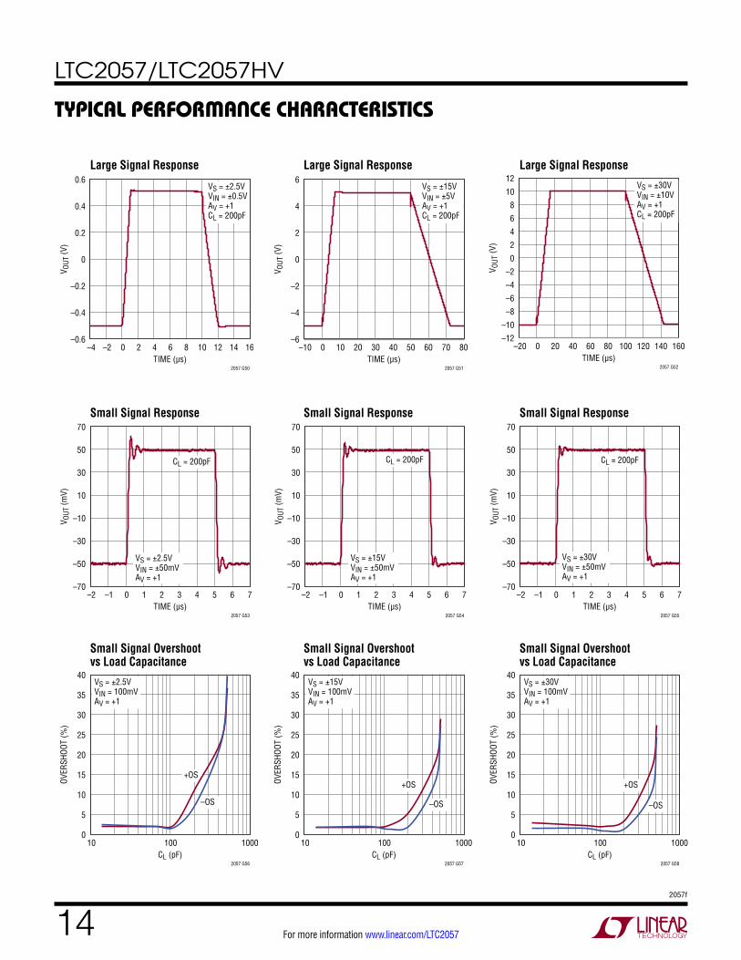
Large Signal Response Large Signal Response Large Signal Response
TIME (µs)–4
–0.6
–0.4
–0.2
0
0.4
0.2
V OUT
(V)
0.6
–2 0 2 10 1664 8 1412
2057 G50
VS = ±2.5VVIN = ±0.5VAV = +1CL = 200pF
TIME (µs)–10
–6
–4
–2
0
4
2
V OUT
(V)
6
0 10 50 803020 40 7060
2057 G51
VS = ±15VVIN = ±5VAV = +1CL = 200pF
TIME (µs)–20
–12
–10
–8
–6
–4
–2
0
10
8
V OUT
(V)
12
4
2
6
0 20 100 1606040 80 140120
2057 G52
VS = ±30VVIN = ±10VAV = +1CL = 200pF
Small Signal Response Small Signal Response Small Signal Response
TIME (µs)–2
–70
–50
–30
–10
10
30
50
V OUT
(mV)
70
–1 0 4 721 3 65
2057 G53
CL = 200pF
VS = ±2.5VVIN = ±50mVAV = +1
TIME (µs)–2
–70
–50
–30
–10
10
30
50
V OUT
(mV)
70
–1 0 4 721 3 65
2057 G54
CL = 200pF
VS = ±15VVIN = ±50mVAV = +1
TIME (µs)–2
–70
–50
–30
–10
10
30
50
V OUT
(mV)
70
–1 0 4 721 3 65
2057 G55
CL = 200pF
VS = ±30VVIN = ±50mVAV = +1
CL (pF)10
0
10
15
20
5
25
35
30
OVER
SHOO
T (%
)
40
100 1000
2057 G56
–OS
+OS
VS = ±2.5VVIN = 100mVAV = +1
Small Signal Overshoot vs Load Capacitance
Small Signal Overshoot vs Load Capacitance
Small Signal Overshoot vs Load Capacitance
CL (pF)10
0
10
15
5
25
35
30
20
OVER
SHOO
T (%
)
40
100 1000
2057 G57
–OS
+OS
VS = ±15VVIN = 100mVAV = +1
CL (pF)10
0
10
15
5
25
35
30
20
OVER
SHOO
T (%
)
40
100 1000
2057 G58
–OS
+OS
VS = ±30VVIN = 100mVAV = +1
LTC2057/LTC2057HV
152057f
For more information www.linear.com/LTC2057
Typical perForMance characTerisTics
TIME (µs)–5
0
V IN
(V)
VOUT (m
V)
2
1
–2
2
6
10
0
4
12
8
0 5 1510 20 6025 30 35 40 45 50 55
2057 G59
AV = –1RF = 10kVS = ±15V
VINVOUTVOUT(AVG)
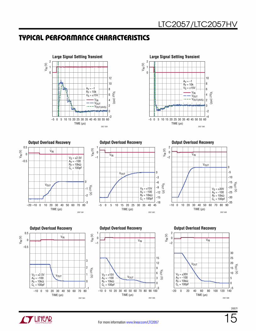
Large Signal Settling Transient Large Signal Settling Transient
TIME (µs)–5
0
V IN
(V)
VOUT (m
V)
2
1
–4
0
4
8
–2
2
10
6
0 5 1510 20 6025 30 35 40 45 50 55
2057 G60
AV = –1RF = 10kVS = ±15V
VINVOUTVOUT(AVG)
Output Overload Recovery Output Overload Recovery Output Overload Recovery
Output Overload Recovery
TIME (µs)–20
V IN
(V)
VOUT (V)
0.5
–0.5
0
–3
–1
–2
0
–10 0 2010 30 8040 50 60 70
2057 G61
VIN
VS = ±2.5VAV = –100RF = 10kΩCL = 100pF
VOUT
TIME (µs)–5
V IN
(V)V
OUT (V)
1
–1
0
–18
–12
–15
–9
–6
–3
0
0 5 1510 20 4525 30 35 40
2057 G62
VOUT
VIN
VS = ±15VAV = –100RF = 10kΩCL = 100pF
TIME (µs)–10
V IN
(V)
VOUT (V)
2
–2
0
–35
–25
0
–30
–20
–15
–10
–5
0 10 3020 40 9050 60 70 80
2057 G63
VOUT
VIN
VS = ±30VAV = –100RF = 10kΩCL = 100pF
TIME (µs)
V IN
(V)
VOUT (V)
0.5
–0.5
0
–1
1
3
0
2
–10 0 2010 30 8040 50 60 70
2057 G64
VOUT
VIN
VS = ±2.5VAV = –100RF = 10kΩCL = 100pF
Output Overload Recovery Output Overload Recovery
TIME (µs)–10
V IN
(V)
VOUT (V)
1
–1
0
–3
3
0
6
9
12
15
0 10 3020 40 10050 60 70 80 90
2057 G65
VOUT
VIN
VS = ±15VAV = –100RF = 10kΩCL = 100pF
TIME (µs)–20
V IN
(V)
VOUT (V)
2
–2
0
–5
5
30
0
10
15
20
25
0 20 6040 80 140100 120
2057 G66
VOUT
VIN
VS = ±30VAV = –100RF = 10kΩCL = 100pF
LTC2057/LTC2057HV
162057f
For more information www.linear.com/LTC2057
pin FuncTionsMS8 and S8/DD8
SD (Pin 1/Pin 1): Shutdown Control Pin.
–IN (Pin 2/Pin 2): Inverting Input.
+IN (Pin 3/Pin 3): Non-Inverting Input.
V– (Pin 4/Pin 4, 9): Negative Power Supply.
MS10
GRD (Pin 1): Guard Ring. No Internal Connection.
–IN (Pin 2): Inverting Input.
+IN (Pin 3): Non-Inverting Input.
GRD (Pin 4): Guard Ring. No Internal Connection.
V– (Pin 5): Negative Power Supply.
SDCOM (Pin 8/Pin 8): Reference Voltage for SD.
V+ (Pin 7/Pin 7): Positive Power Supply.
OUT (Pin 6/Pin 6): Amplifier Output
NC (Pin 5/Pin 5): No Internal Connection.
SD (Pin 10): Shutdown Control Pin.
SDCOM (Pin 9): Reference Voltage for SD.
V+ (Pin 8): Positive Power Supply.
NC (Pin 7): No Internal Connection.
OUT (Pin 6): Amplifier Output.
LTC2057/LTC2057HV
172057f
For more information www.linear.com/LTC2057
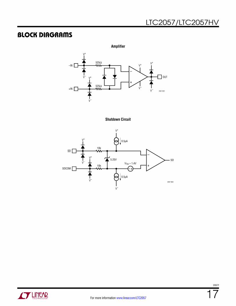
block DiagraMs
10k
10k
SD
SDCOM
2057 BD2
V+
V–
V+
V–
0.5µA
0.5µA
5.25VVTH ≈ 1.4V
V+
V–
SD
+
–
+–
Amplifier
Shutdown Circuit
V+
V–525Ω
525Ω–IN
+IN2057 BD1
V+
V–V+
V–
+
–OUT
V+
V–
LTC2057/LTC2057HV
182057f
For more information www.linear.com/LTC2057
applicaTions inForMaTionInput Voltage Noise
Chopper stabilized amplifiers like the LTC2057 achieve low offset and 1/f noise by heterodyning DC and flicker noise to higher frequencies. In a classical chopper stabilized amplifier, this process results in idle tones at the chopping frequency and its odd harmonics.
The LTC2057 utilizes circuitry to suppress these spurious artifacts to well below the offset voltage. The typical ripple magnitude at 100kHz is much less than 1µVRMS.
The voltage noise spectrum of the LTC2057 is shown in Figure 1. If lower noise is required, consider one of the following circuits from the Typical Applications section: "DC Stabilized, Ultralow Noise Amplifier" or "Paralleling Choppers to Improve Noise."
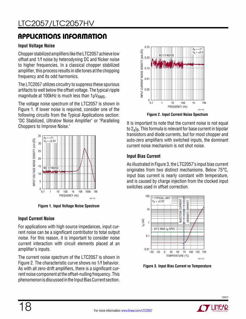
It is important to note that the current noise is not equal to 2qIB. This formula is relevant for base current in bipolar transistors and diode currents, but for most chopper and auto-zero amplifiers with switched inputs, the dominant current noise mechanism is not shot noise.
Input Bias Current
As illustrated in Figure 3, the LTC2057’s input bias current originates from two distinct mechanisms. Below 75°C, input bias current is nearly constant with temperature, and is caused by charge injection from the clocked input switches used in offset correction.
Figure 1. Input Voltage Noise Spectrum
Input Current Noise
For applications with high source impedances, input cur-rent noise can be a significant contributor to total output noise. For this reason, it is important to consider noise current interaction with circuit elements placed at an amplifier’s inputs.
The current noise spectrum of the LTC2057 is shown in Figure 2. The characteristic curve shows no 1/f behavior. As with all zero-drift amplifiers, there is a significant cur-rent noise component at the offset-nulling frequency. This phenomenon is discussed in the Input Bias Current section.
Figure 2. Input Current Noise Spectrum
Figure 3. Input Bias Current vs Temperature
FREQUENCY (Hz)0.1
0
5
10
15
20
INPU
T VO
LTAG
E NO
ISE
DENS
ITY
(nV/
√Hz)
25
30
35
1 10 100 1k 10k 100k 1M
2057 F01
AV = +11VS = ±2.5V
NO 1/f NOISE
FREQUENCY (Hz)0.1
0
0.05
0.01
0.15
0.20
INPU
T CU
RREN
T NO
ISE
DENS
ITY
(pA/
√Hz)
0.25
1 10 100 1k 10k
2057 F02
NO 1/f NOISE
AV = +11VS = ±2.5
TEMPERATURE (°C)–50
0.01
0.1
1
10
I B (n
A)
100
–25 0 25 50 75 100 125 150
2057 F03
LEAKAGE CURRENT
25°C MAX IB SPEC
INJE
CTIO
N CU
RREN
T1 TYPICAL UNITVS = ±2.5V
LTC2057/LTC2057HV
192057f
For more information www.linear.com/LTC2057
applicaTions inForMaTionThe DC average of injection current is the specified input bias current, but this current has a frequency component at the chopping frequency as well. When these small current pulses, typically about 0.7nARMS, interact with source impedances or gain setting resistors, the resulting voltage spikes are amplified by the closed loop gain. For high impedances, this may cause the 100kHz chopping frequency to be visible in the output spectrum, which is a phenomenon known as clock feed-through.
For zero-drift amplifiers, clock feed-through will be proportional to source impedance and the magnitude of injection current, a measure of which is IB at 25°C. In order to minimize clock feed-through, keep gain-setting resistors and source impedances as low as possible. If high impedances are required, place a capacitor across the feedback resistor to limit the bandwidth of the closed loop gain. Doing so will effectively filter out the clock feed-through signal.
Injection currents from the two inputs are of equal magni-tude but opposite direction. Therefore, input bias current effects due to injection currents will not be canceled by placing matched impedances at both inputs.
Above 75°C, leakage of the ESD protection diodes begins to dominate the input bias current and continues to increase exponentially at elevated temperatures. Unlike injection current, leakage currents are in the same direction for both inputs. Therefore, the output error due to leakage currents
can be mitigated by matching the source impedances seen by the two inputs.
Thermocouple Effects
In order to achieve accuracy on the microvolt level, ther-mocouple effects must be considered. Any connection of dissimilar metals forms a thermoelectric junction and generates a small temperature-dependent voltage. Also known as the Seebeck Effect, these thermal EMFs can be the dominant error source in low-drift circuits.
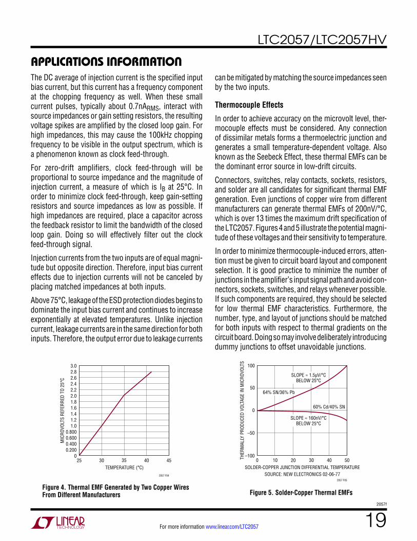
Connectors, switches, relay contacts, sockets, resistors, and solder are all candidates for significant thermal EMF generation. Even junctions of copper wire from different manufacturers can generate thermal EMFs of 200nV/°C, which is over 13 times the maximum drift specification of the LTC2057. Figures 4 and 5 illustrate the potential magni-tude of these voltages and their sensitivity to temperature.
In order to minimize thermocouple-induced errors, atten-tion must be given to circuit board layout and component selection. It is good practice to minimize the number of junctions in the amplifier’s input signal path and avoid con-nectors, sockets, switches, and relays whenever possible. If such components are required, they should be selected for low thermal EMF characteristics. Furthermore, the number, type, and layout of junctions should be matched for both inputs with respect to thermal gradients on the circuit board. Doing so may involve deliberately introducing dummy junctions to offset unavoidable junctions.
Figure 4. Thermal EMF Generated by Two Copper Wires From Different Manufacturers Figure 5. Solder-Copper Thermal EMFs
TEMPERATURE (°C)25
MIC
ROVO
LTS
REFE
RRED
TO
25°C
1.8
2.4
3.02.82.6
2.02.2
1.41.6
0.8001.0
0.2000.400
30 40 45
2057 F04
1.2
0.600
035
SOLDER-COPPER JUNCTION DIFFERENTIAL TEMPERATURESOURCE: NEW ELECTRONICS 02-06-77
0THER
MAL
LY P
RODU
CED
VOLT
AGE
IN M
ICRO
VOLT
S
0
50
40
2057 F05
–50
–10010 20 30 50
100
SLOPE ≈ 1.5µV/°CBELOW 25°C
SLOPE ≈ 160nV/°CBELOW 25°C
64% SN/36% Pb
60% Cd/40% SN
LTC2057/LTC2057HV
202057f
For more information www.linear.com/LTC2057
applicaTions inForMaTion
Figure 7a. Example Layout of Non-Inverting Amplifier with Leakage Guard Ring
LEAKAGECURRENT
HIGH-ZSENSOR
GUARDRING
NO SOLDER MASKOVER GUARD RING
V–
V–
GRD
+IN
GRD
–IN
OUT
NC
V+ V+
VOUT
SD
SDCOM
*
* NO LEAKAGE CURRENT. V+IN = VGRD** VERROR = ILEAK • RG; RG << ZSENSOR
RF
VBIAS
RG**
2057 F07a
+
–
RIN
HIGH-Z SENSOR
GUARD RING
† LEAKAGE CURRENT
ALTERNATIVEGUARD RING
DRIVE
ALTERNATIVE GUARD RINGDRIVE CIRCUIT IF RG MUST BE HIGH IMPEDANCE.
†
VIN
VOUTVBIAS
RG
RF
LTC2057
R´F
+–
V+
V–
R GRFRG
= R'FR'G
; R'G << RG
LTC2057MS10
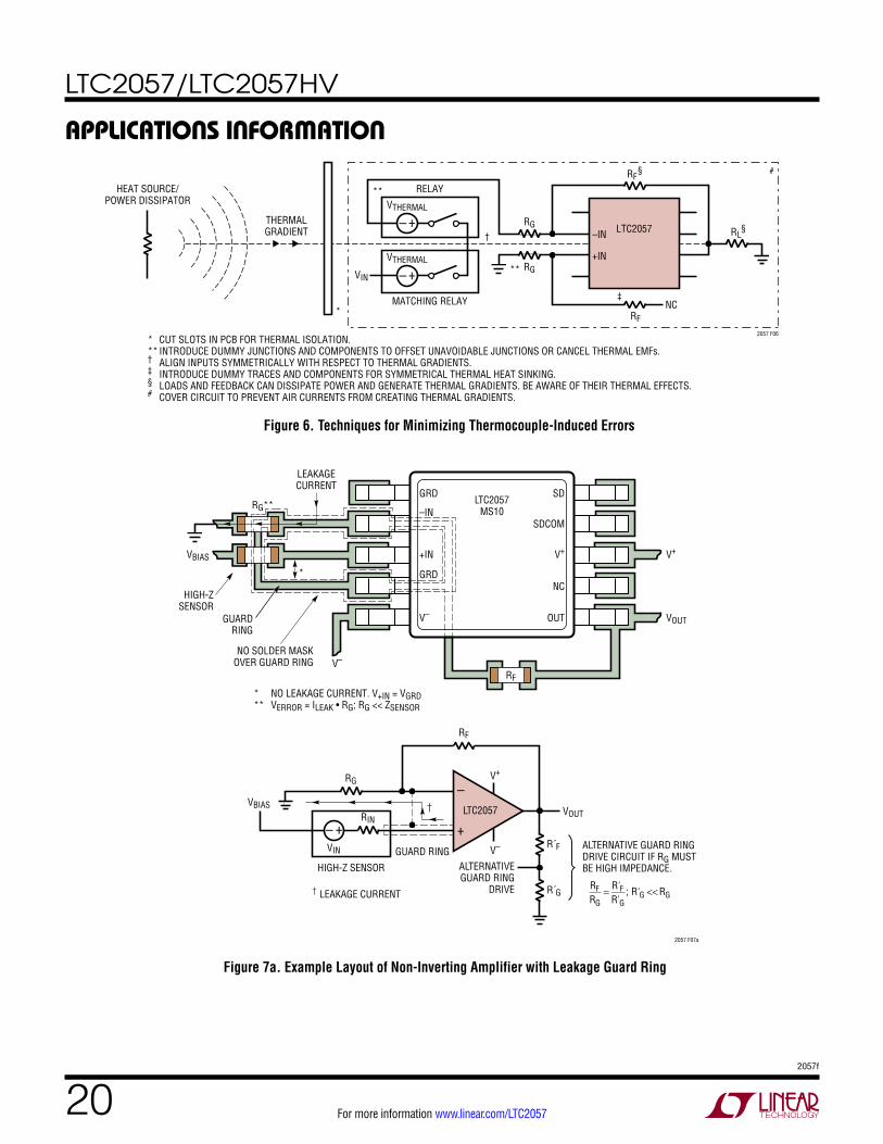
Figure 6. Techniques for Minimizing Thermocouple-Induced Errors
LTC2057THERMALGRADIENT
RELAY
MATCHING RELAY NC
* CUT SLOTS IN PCB FOR THERMAL ISOLATION.** INTRODUCE DUMMY JUNCTIONS AND COMPONENTS TO OFFSET UNAVOIDABLE JUNCTIONS OR CANCEL THERMAL EMFs.† ALIGN INPUTS SYMMETRICALLY WITH RESPECT TO THERMAL GRADIENTS.‡ INTRODUCE DUMMY TRACES AND COMPONENTS FOR SYMMETRICAL THERMAL HEAT SINKING.§ LOADS AND FEEDBACK CAN DISSIPATE POWER AND GENERATE THERMAL GRADIENTS. BE AWARE OF THEIR THERMAL EFFECTS.# COVER CIRCUIT TO PREVENT AIR CURRENTS FROM CREATING THERMAL GRADIENTS.
HEAT SOURCE/POWER DISSIPATOR
RL§
–IN
+IN
RF§
RG
RF
VIN
*
RG
2057 F06
**
†
‡
**
#
+–
+–
VTHERMAL
VTHERMAL
LTC2057/LTC2057HV
212057f
For more information www.linear.com/LTC2057
applicaTions inForMaTion
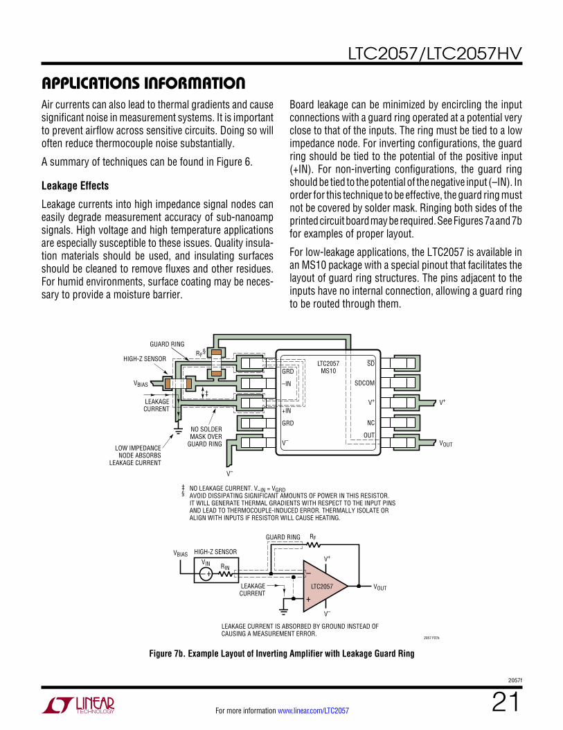
Figure 7b. Example Layout of Inverting Amplifier with Leakage Guard Ring
HIGH-Z SENSOR
LOW IMPEDANCENODE ABSORBS
LEAKAGE CURRENT
GUARD RING
LEAKAGECURRENT
V–
V–
GRD
+IN
GRD
–IN
OUT
NC
V+ V+
VOUT
SD
SDCOM
‡
‡ NO LEAKAGE CURRENT. V–IN = VGRD§ AVOID DISSIPATING SIGNIFICANT AMOUNTS OF POWER IN THIS RESISTOR. IT WILL GENERATE THERMAL GRADIENTS WITH RESPECT TO THE INPUT PINS AND LEAD TO THERMOCOUPLE-INDUCED ERROR. THERMALLY ISOLATE OR ALIGN WITH INPUTS IF RESISTOR WILL CAUSE HEATING.
VBIAS
RF§
2057 F07b
LTC2057MS10
NO SOLDERMASK OVER
GUARD RING
+
–
GUARD RING
LTC2057LEAKAGECURRENT
LEAKAGE CURRENT IS ABSORBED BY GROUND INSTEAD OFCAUSING A MEASUREMENT ERROR.
VOUT
V+
V–
HIGH-Z SENSOR
RF
VBIAS
+–VIN RIN
Air currents can also lead to thermal gradients and cause significant noise in measurement systems. It is important to prevent airflow across sensitive circuits. Doing so will often reduce thermocouple noise substantially.
A summary of techniques can be found in Figure 6.
Leakage Effects
Leakage currents into high impedance signal nodes can easily degrade measurement accuracy of sub-nanoamp signals. High voltage and high temperature applications are especially susceptible to these issues. Quality insula-tion materials should be used, and insulating surfaces should be cleaned to remove fluxes and other residues. For humid environments, surface coating may be neces-sary to provide a moisture barrier.
Board leakage can be minimized by encircling the input connections with a guard ring operated at a potential very close to that of the inputs. The ring must be tied to a low impedance node. For inverting configurations, the guard ring should be tied to the potential of the positive input (+IN). For non-inverting configurations, the guard ring should be tied to the potential of the negative input (–IN). In order for this technique to be effective, the guard ring must not be covered by solder mask. Ringing both sides of the printed circuit board may be required. See Figures 7a and 7b for examples of proper layout.
For low-leakage applications, the LTC2057 is available in an MS10 package with a special pinout that facilitates the layout of guard ring structures. The pins adjacent to the inputs have no internal connection, allowing a guard ring to be routed through them.
LTC2057/LTC2057HV
222057f
For more information www.linear.com/LTC2057
applicaTions inForMaTionPower Dissipation
Since the LTC2057/LTC2057HV is capable of operating at >30V total supply, care should be taken with respect to power dissipation in the amplifier. When driving heavy loads at high voltages, use the θJA of the package to estimate the resulting die-temperature rise and take measures to ensure that the resulting junction temperature does not exceed specified limits. PCB metallization and heat sinking should also be considered when high power dissipation is expected. Thermal information for all packages can be found in the Pin Configuration section.
Electrical Overstress
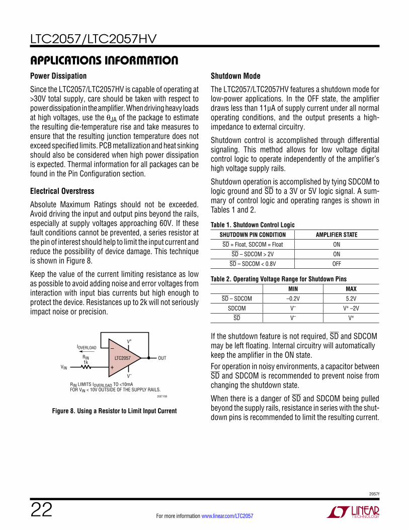
Absolute Maximum Ratings should not be exceeded. Avoid driving the input and output pins beyond the rails, especially at supply voltages approaching 60V. If these fault conditions cannot be prevented, a series resistor at the pin of interest should help to limit the input current and reduce the possibility of device damage. This technique is shown in Figure 8.
Keep the value of the current limiting resistance as low as possible to avoid adding noise and error voltages from interaction with input bias currents but high enough to protect the device. Resistances up to 2k will not seriously impact noise or precision.
Shutdown Mode
The LTC2057/LTC2057HV features a shutdown mode for low-power applications. In the OFF state, the amplifier draws less than 11μA of supply current under all normal operating conditions, and the output presents a high-impedance to external circuitry.
Shutdown control is accomplished through differential signaling. This method allows for low voltage digital control logic to operate independently of the amplifier’s high voltage supply rails.
Shutdown operation is accomplished by tying SDCOM to logic ground and SD to a 3V or 5V logic signal. A sum-mary of control logic and operating ranges is shown in Tables 1 and 2.
Table 1. Shutdown Control LogicSHUTDOWN PIN CONDITION AMPLIFIER STATE
SD = Float, SDCOM = Float ON
SD – SDCOM > 2V ON
SD – SDCOM < 0.8V OFF
Table 2. Operating Voltage Range for Shutdown PinsMIN MAX
SD – SDCOM –0.2V 5.2V
SDCOM V– V+ –2V
SD V– V+
If the shutdown feature is not required, SD and SDCOM may be left floating. Internal circuitry will automatically keep the amplifier in the ON state.For operation in noisy environments, a capacitor between SD and SDCOM is recommended to prevent noise from changing the shutdown state.
When there is a danger of SD and SDCOM being pulled beyond the supply rails, resistance in series with the shut-down pins is recommended to limit the resulting current.
Figure 8. Using a Resistor to Limit Input Current
2057 F08
+
–
RIN LIMITS IOVERLOAD TO <10mA FOR VIN < 10V OUTSIDE OF THE SUPPLY RAILS.
OUTLTC2057
VIN
V+
V–
RIN1k
IOVERLOAD
LTC2057/LTC2057HV
232057f
For more information www.linear.com/LTC2057
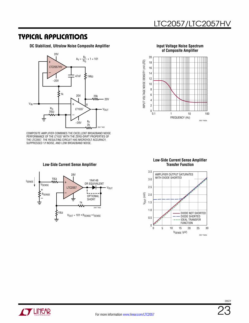
Typical applicaTionsDC Stabilized, Ultralow Noise Composite Amplifier
Low-Side Current Sense Amplifier
2057 TA02
RG20Ω
VIN
VOUT
20V
20V20V
20k
RF2k
47nF
1k
8
–20V
–20V
LTC2057HV
+
–
LT1037
+
–
1MΩ
AV =RFRG
+ 1 = 101
COMPOSITE AMPLIFIER COMBINES THE EXCELLENT BROADBAND NOISE PERFORMANCE OF THE LT1037 WITH THE ZERO-DRIFT PROPERTIES OF THE LTC2057. THE RESULTING CIRCUIT HAS MICROVOLT ACCURACY, SUPPRESSED 1/f NOISE, AND LOW BROADBAND NOISE.
2057 TA03
+
–
10Ω
1k
28V
1N4148 OR EQUIVALENT
OPTIONALSHORT
VOUT
VOUT = 101 • RSENSE • ISENSE
LTC2057VSENSE
ISENSE
10Ω
RSENSE
+
–
FREQUENCY (Hz)0.1 1
0
10
INPU
T VO
LTAG
E NO
ISE
DENS
ITY
(nV/
√Hz)
20
18
16
14
12
8
6
4
2
10 100
2057 TA02b
Low-Side Current Sense Amplifier Transfer Function
Input Voltage Noise Spectrumof Composite Amplifier
VSENSE (µV)0
0
1.0
2.0
3.0
V OUT
(mV)
3.5
0.5
1.5
2.5
5 10 2015 25 30
2057 TA03b
DIODE NOT SHORTEDDIODE SHORTEDIDEAL TRANSFER FUNCTION
AMPLIFIER OUTPUT SATURATESWITH DIODE SHORTED
LTC2057/LTC2057HV
242057f
For more information www.linear.com/LTC2057
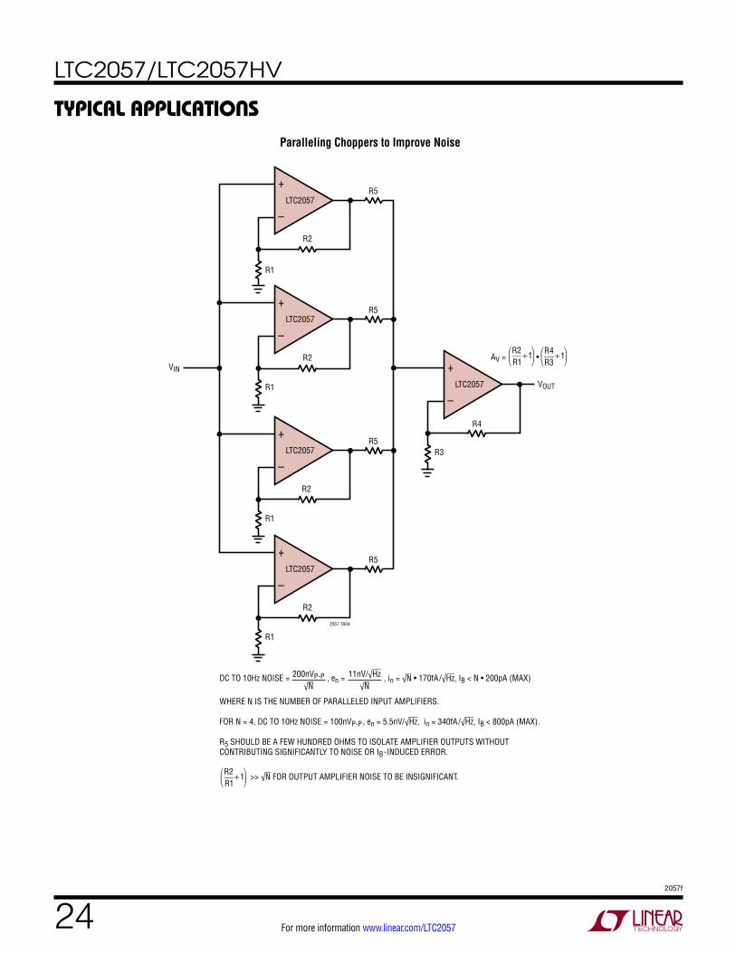
Typical applicaTionsParalleling Choppers to Improve Noise
–
+R5
R2
R1
R1
LTC2057
VIN
VOUT
2057 TA04
–
+R5
R2
LTC2057
R1
–
+R5
R2
LTC2057
R1
DC TO 10Hz NOISE =
WHERE N IS THE NUMBER OF PARALLELED INPUT AMPLIFIERS.
FOR N = 4, DC TO 10Hz NOISE = 100nVP-P , en = 5.5nV/√Hz, in = 340fA/√Hz, IB < 800pA (MAX).
R5 SHOULD BE A FEW HUNDRED OHMS TO ISOLATE AMPLIFIER OUTPUTS WITHOUT CONTRIBUTING SIGNIFICANTLY TO NOISE OR IB-INDUCED ERROR.
, in = √N • 170fA/√Hz, IB < N • 200pA (MAX), en =200nVP-P√N
–
+R5
R2
LTC2057
R3
–
+
R4
LTC2057
11nV/√Hz√N
AV = • R2R1
+1 R4R3
+1
>> √N FOR OUTPUT AMPLIFIER NOISE TO BE INSIGNIFICANT.R2R1
+1

LTC2057/LTC2057HV
252057f
For more information www.linear.com/LTC2057
Typical applicaTions
Ultra-Precision, 135dB Dynamic Range Photodiode Amplifier Output Noise Spectrum of Photodiode Amplifier
NOISE FLOOR IS ONLY SLIGHTLY ABOVE THE 20kΩ RESISTOR`S 18nV/√Hz.CLOCK FEEDTHROUGH IS VISIBLE NEAR 100kHz WITH AMPLITUDE OF 10µVRMS OUTPUT REFERRED OR 0.5nARMS INPUT REFERRED.
Wide Input Range Precision Gain-of-100 Instrumentation Amplifier
–
+
52V
–1V
68pFPD
IPD
VOUT
20k
30pF
LTC2057HV
2057 TA06
VOUT = IPD • 20kΩBW = 300kHz
OUTPUT RANGE 9µV TO 50V, LIMIT BW TO 1kHz TO KEEP OUTPUT NOISE BELOW 5µVP-P
FREQUENCY (Hz)1k
0
OUTP
UT N
OISE
VOL
TAGE
DEN
SITY
(nV/
√Hz)
320
280
200
160
240
120
80
40
400
360
100k
2057 TA06b
10k
RBW = 1kHz
30V
–30V
–IN
+IN
30V
11.5k
11.5k
–30V
2057 TA01a
LTC2057HV
LTC2057HV
M9M3M1
INPUT CM RANGE = ±28V WITH 4V OF OUTPUT SWINGCMRR = 130dB (TYP), INPUT OFFSET VOLTAGE = 1µV (TYP)
+
–
–
+
89
10
P1P3P9
LT1991A
18V
–18V
REF
OUT6
54
7
VOUT
VCC
VEE
232Ω123
LTC2057/LTC2057HV
262057f
For more information www.linear.com/LTC2057
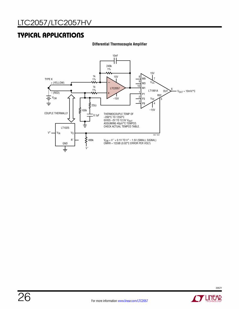
Typical applicaTionsDifferential Thermocouple Amplifier
V–
–15V
–15V
15V15V
GND
VINV+ VO
R–
LT1025
2057 TA07
+ (YELLOW)
– (RED)
499k
–
+LTC2057
LT1991A
VCC
VEE
REFOUT
M9
M3
M1
7
6VOUT = 10mV/°C
VCM
10nF
249k1%
1k1%
22Ω
0.1µF
1k1%
P1
P3
P9
8
9
10
1
2
3
100kCOUPLE THERMALLY
TYPE K
THERMOCOUPLE TEMP OF–200°C TO 1250°CGIVES –2V TO 12.5V VOUTASSUMING 40µV/°C TEMPCO.CHECK ACTUAL TEMPCO TABLE.
VCM = V– + 0.1V TO V+ – 1.5V (SMALL SIGNAL)CMRR = 122dB (0.02°C ERROR PER VOLT)
5
4

LTC2057/LTC2057HV
272057f
For more information www.linear.com/LTC2057
Typical applicaTions18-Bit DAC with ±25V Output Swing
2057 TA08
30V
–30V
8pF
30V
–30V
VOUT
+
–
RFB
IOUT1
IOUT2
GND
ROFSRCOMRIN
VDD
GND
REF
LTC2057HV
–
+LTC2057HV
LT5400-110kΩ MATCHEDRESISTOR NETWORK
+
–LT1012
150pF
5V LTC275618-BIT DAC WITH SPAN SELECT
SET SPAN TO ±10V0.1µF
4
SPI WITHREADBACK
REF5V
Time Domain Response
TIME (50µs/DIV)
V CS/
LD (V
) 10
0
5
–30
–20
–10
0
10
20
30
2057 TA09
VOUT
VCS/LD
VOUT (V)
LTC2057/LTC2057HV
282057f
For more information www.linear.com/LTC2057
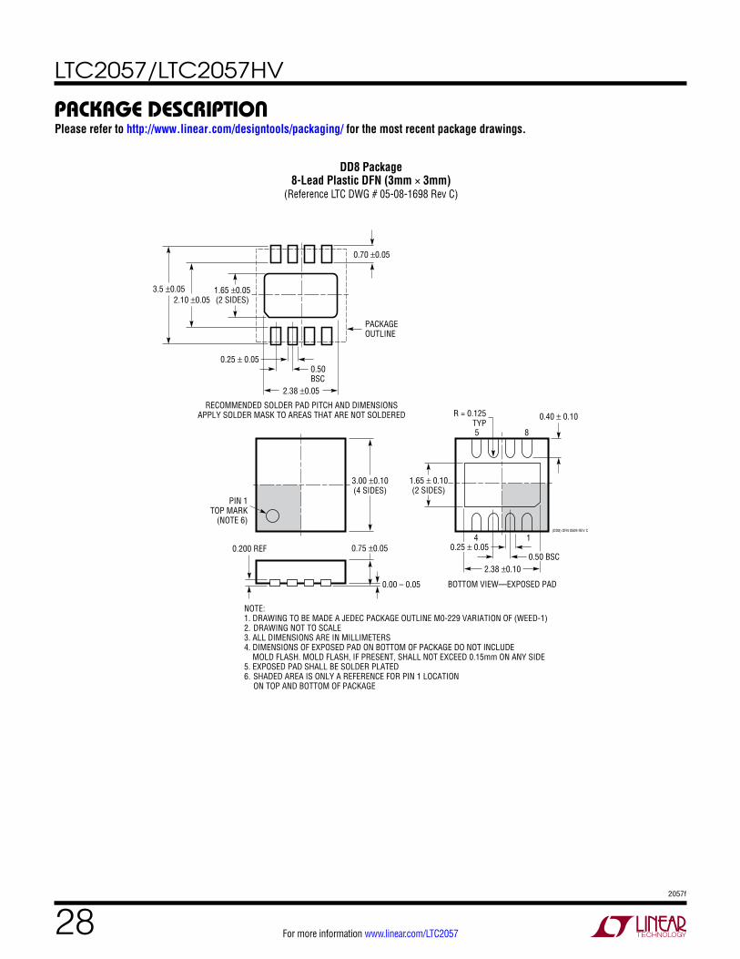
package DescripTion
DD8 Package8-Lead Plastic DFN (3mm × 3mm)
(Reference LTC DWG # 05-08-1698 Rev C)
3.00 ±0.10(4 SIDES)
NOTE:1. DRAWING TO BE MADE A JEDEC PACKAGE OUTLINE M0-229 VARIATION OF (WEED-1)2. DRAWING NOT TO SCALE3. ALL DIMENSIONS ARE IN MILLIMETERS4. DIMENSIONS OF EXPOSED PAD ON BOTTOM OF PACKAGE DO NOT INCLUDE MOLD FLASH. MOLD FLASH, IF PRESENT, SHALL NOT EXCEED 0.15mm ON ANY SIDE5. EXPOSED PAD SHALL BE SOLDER PLATED6. SHADED AREA IS ONLY A REFERENCE FOR PIN 1 LOCATION ON TOP AND BOTTOM OF PACKAGE
0.40 ± 0.10
BOTTOM VIEW—EXPOSED PAD
1.65 ± 0.10(2 SIDES)
0.75 ±0.05
R = 0.125TYP
2.38 ±0.10
14
85
PIN 1TOP MARK
(NOTE 6)
0.200 REF
0.00 – 0.05
(DD8) DFN 0509 REV C
0.25 ± 0.05
2.38 ±0.05
RECOMMENDED SOLDER PAD PITCH AND DIMENSIONSAPPLY SOLDER MASK TO AREAS THAT ARE NOT SOLDERED
1.65 ±0.05(2 SIDES)2.10 ±0.05
0.50BSC
0.70 ±0.05
3.5 ±0.05
PACKAGEOUTLINE
0.25 ± 0.050.50 BSC
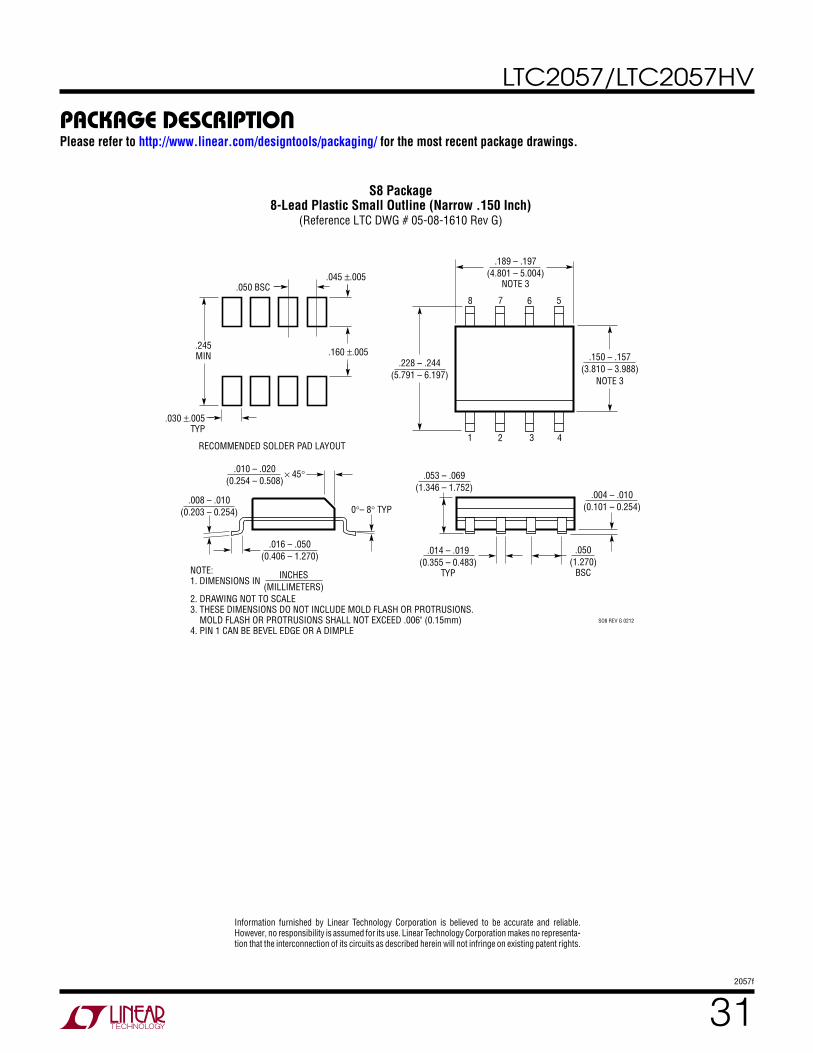
Please refer to http://www.linear.com/designtools/packaging/ for the most recent package drawings.
LTC2057/LTC2057HV
292057f
For more information www.linear.com/LTC2057
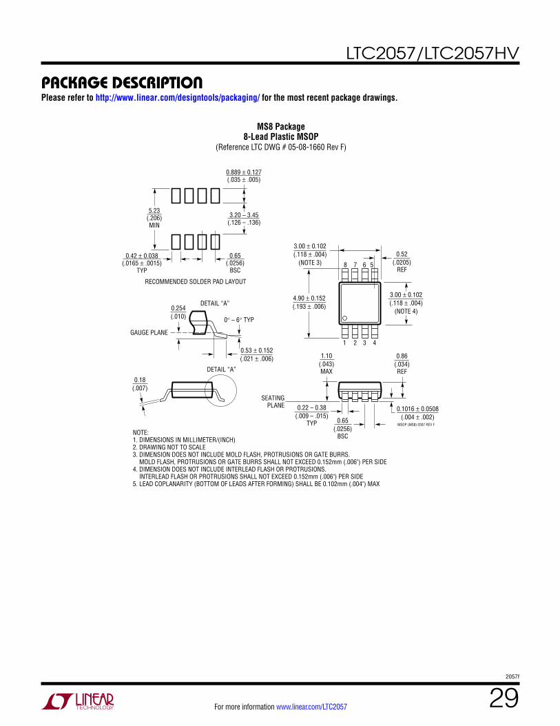
package DescripTion
MS8 Package8-Lead Plastic MSOP
(Reference LTC DWG # 05-08-1660 Rev F)
MSOP (MS8) 0307 REV F
0.53 ± 0.152(.021 ± .006)
SEATINGPLANE
NOTE:1. DIMENSIONS IN MILLIMETER/(INCH)2. DRAWING NOT TO SCALE3. DIMENSION DOES NOT INCLUDE MOLD FLASH, PROTRUSIONS OR GATE BURRS. MOLD FLASH, PROTRUSIONS OR GATE BURRS SHALL NOT EXCEED 0.152mm (.006") PER SIDE4. DIMENSION DOES NOT INCLUDE INTERLEAD FLASH OR PROTRUSIONS. INTERLEAD FLASH OR PROTRUSIONS SHALL NOT EXCEED 0.152mm (.006") PER SIDE5. LEAD COPLANARITY (BOTTOM OF LEADS AFTER FORMING) SHALL BE 0.102mm (.004") MAX
0.18(.007)
0.254(.010)
1.10(.043)MAX
0.22 – 0.38(.009 – .015)
TYP
0.1016 ± 0.0508(.004 ± .002)
0.86(.034)REF
0.65(.0256)
BSC
0° – 6° TYP
DETAIL “A”
DETAIL “A”
GAUGE PLANE
1 2 3 4
4.90 ± 0.152(.193 ± .006)
8 7 6 5
3.00 ± 0.102(.118 ± .004)
(NOTE 3)
3.00 ± 0.102(.118 ± .004)
(NOTE 4)
0.52(.0205)
REF
5.23(.206)MIN
3.20 – 3.45(.126 – .136)
0.889 ± 0.127(.035 ± .005)
RECOMMENDED SOLDER PAD LAYOUT
0.42 ± 0.038(.0165 ± .0015)
TYP
0.65(.0256)
BSC
Please refer to http://www.linear.com/designtools/packaging/ for the most recent package drawings.
LTC2057/LTC2057HV
302057f
For more information www.linear.com/LTC2057
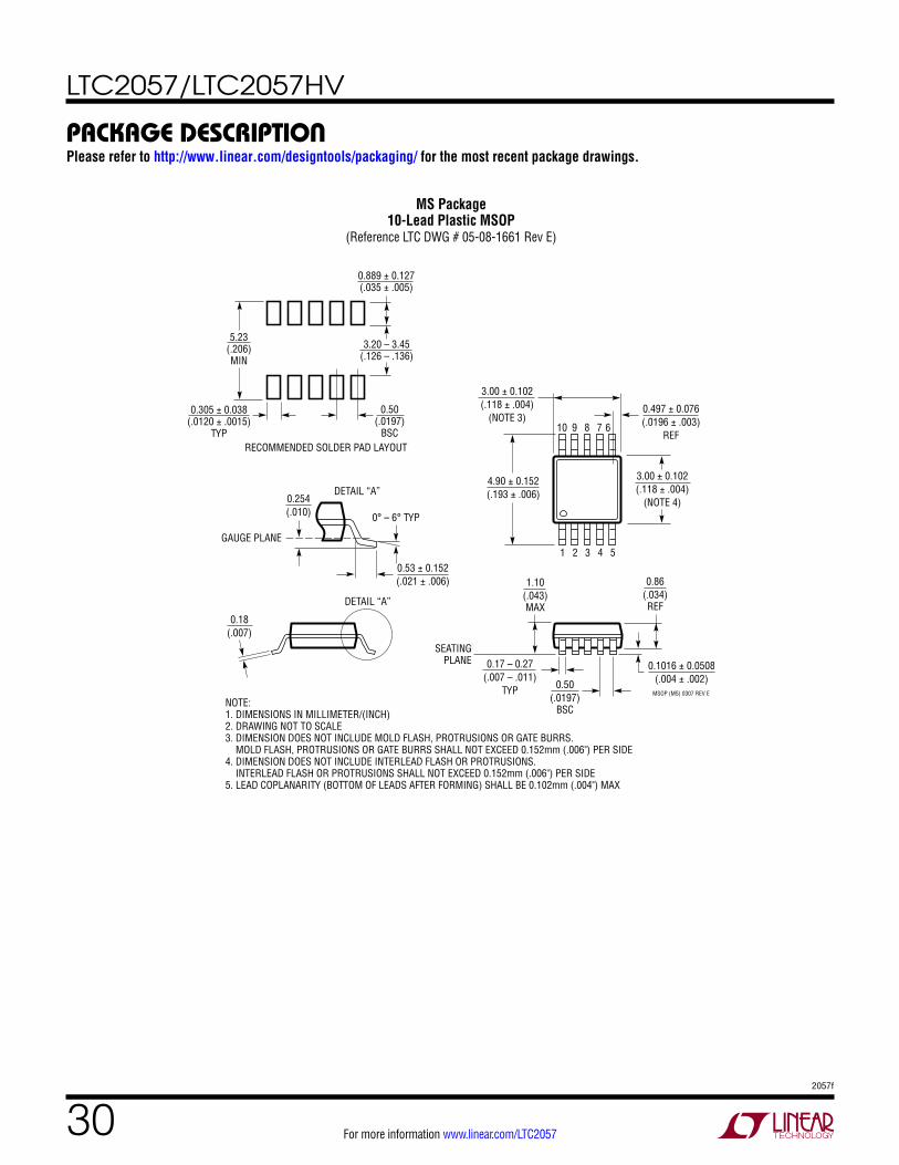
package DescripTion
MS Package10-Lead Plastic MSOP
(Reference LTC DWG # 05-08-1661 Rev E)
MSOP (MS) 0307 REV E
0.53 ± 0.152(.021 ± .006)
SEATINGPLANE
0.18(.007)
1.10(.043)MAX
0.17 – 0.27(.007 – .011)
TYP
0.86(.034)REF
0.50(.0197)
BSC
1 2 3 4 5
4.90 ± 0.152(.193 ± .006)
0.497 ± 0.076(.0196 ± .003)
REF8910 7 6
3.00 ± 0.102(.118 ± .004)
(NOTE 3)
3.00 ± 0.102(.118 ± .004)
(NOTE 4)
NOTE:1. DIMENSIONS IN MILLIMETER/(INCH)2. DRAWING NOT TO SCALE3. DIMENSION DOES NOT INCLUDE MOLD FLASH, PROTRUSIONS OR GATE BURRS. MOLD FLASH, PROTRUSIONS OR GATE BURRS SHALL NOT EXCEED 0.152mm (.006") PER SIDE4. DIMENSION DOES NOT INCLUDE INTERLEAD FLASH OR PROTRUSIONS. INTERLEAD FLASH OR PROTRUSIONS SHALL NOT EXCEED 0.152mm (.006") PER SIDE5. LEAD COPLANARITY (BOTTOM OF LEADS AFTER FORMING) SHALL BE 0.102mm (.004") MAX
0.254(.010) 0° – 6° TYP
DETAIL “A”
DETAIL “A”
GAUGE PLANE
5.23(.206)MIN
3.20 – 3.45(.126 – .136)
0.889 ± 0.127(.035 ± .005)
RECOMMENDED SOLDER PAD LAYOUT
0.305 ± 0.038(.0120 ± .0015)
TYP
0.50(.0197)
BSC
0.1016 ± 0.0508(.004 ± .002)
Please refer to http://www.linear.com/designtools/packaging/ for the most recent package drawings.
LTC2057/LTC2057HV
312057f
Information furnished by Linear Technology Corporation is believed to be accurate and reliable. However, no responsibility is assumed for its use. Linear Technology Corporation makes no representa-tion that the interconnection of its circuits as described herein will not infringe on existing patent rights.
package DescripTionPlease refer to http://www.linear.com/designtools/packaging/ for the most recent package drawings.
.016 – .050(0.406 – 1.270)
.010 – .020(0.254 – 0.508)
× 45°
0°– 8° TYP.008 – .010
(0.203 – 0.254)
SO8 REV G 0212
.053 – .069(1.346 – 1.752)
.014 – .019(0.355 – 0.483)
TYP
.004 – .010(0.101 – 0.254)
.050(1.270)
BSC
1 2 3 4
.150 – .157(3.810 – 3.988)
NOTE 3
8 7 6 5
.189 – .197(4.801 – 5.004)
NOTE 3
.228 – .244(5.791 – 6.197)
.245MIN .160 ±.005
RECOMMENDED SOLDER PAD LAYOUT
.045 ±.005 .050 BSC
.030 ±.005 TYP
INCHES(MILLIMETERS)
NOTE:1. DIMENSIONS IN
2. DRAWING NOT TO SCALE3. THESE DIMENSIONS DO NOT INCLUDE MOLD FLASH OR PROTRUSIONS. MOLD FLASH OR PROTRUSIONS SHALL NOT EXCEED .006" (0.15mm)4. PIN 1 CAN BE BEVEL EDGE OR A DIMPLE
S8 Package8-Lead Plastic Small Outline (Narrow .150 Inch)
(Reference LTC DWG # 05-08-1610 Rev G)
LTC2057/LTC2057HV
322057f
Linear Technology Corporation1630 McCarthy Blvd., Milpitas, CA 95035-7417 (408) 432-1900 FAX: (408) 434-0507 www.linear.com/LTC2057 LINEAR TECHNOLOGY CORPORATION 2013
LT 0513 • PRINTED IN USA
relaTeD parTs
Typical applicaTion
PART NUMBER DESCRIPTION COMMENTS
LTC2050HV Zero-Drift Operational Amplifier 3µV VOS, 2.7V to 12V VS, 1.5mA IS, RR Output
LTC2051HV/LTC2052HV
Dual/Quad, Zero-Drift Operational Amplifier 3µV VOS, 2.7V to 12V VS, 1.5mA IS, RR Output
LTC2053 Precision, Rail-to-Rail, Zero-Drift, Resistor-Programmable Instrumentation Amplifier
10µV VOS, 2.7V to 11V VS, 1.3mA IS, RRIO
LTC2054HV/LTC2055HV
Micropower, Single/Dual, Zero-Drift Operational Amplifier 5µV VOS, 2.7V to 12V VS, 0.2mA IS, RRIO
LTC6652 Precision, Low Drift, Low Noise, Buffered Reference 5ppm/°C, 0.05% Initial Accuracy, 2.1ppmP-P Noise
LT6654 Precision, Wide Supply, High Output Drive, Low Noise Reference 10ppm/°C, 0.05% Initial Accuracy, 1.6ppmP-P Noise
LTC6655 0.25ppm Noise, Low Drift, Precision, Buffered Reference Family 2ppm/°C, 0.025% Initial Accuracy, 0.25ppmP-P Noise
LT6016/LT6017 Dual/Quad, 76V Over-The-Top® Input Operational Amplifier 50µV VOS, 3V to 50V VS, 0.335mA IS, RRIO
LTC6090 140V Operational Amplifier 50pA IB, 1.6mV VOS, 9.5V to 140V VS, 4.5mA IS, RR Output
LT5400 Quad Matched Resistor Network ±0.01%, ±0.2ppm/°C Matching
Microvolt Precision 18-Bit ADC Driver
+
–
5V
–5V
–5V
2.5V 1.8V
10k 10Ω1%
150Ω
205Ω
50mV
0VLTC2057
2057 TA10
10nF
1µF
100k1%
SAMPLE
CHAINRDL/SDI
SDOSCK
BUSYCNV
+IN
–IN
VDD
REF
OVDD
GND
0.1µF10µF
LTC6655-2.5
LTC2368-18
GND
VIN
SHDN
VOUT_F
VOUT_S47µF
5V
AV = 50BW = 1kHz
≤ 5 ksps IS RECOMMENDED TO MINIMIZE ERROR FROM ADC INPUT CURRENT AND 150Ω RESISTOR.
RESISTOR DIVIDER AT ADC INPUT ENSURES LIVE ZERO OPERATION BY ACCOUNTING FOR 5µV MAXIMUM VOS OF THE LTC2057 AND 11LSB ZERO-SCALE ERROR OF THE ADC. RESULTING OFFSET IS CONSTANT AND CAN BE SUBTRACTED FROM THE RESULT.