ltc1863/ltc1867 12-/16-bit, 8-channel 200ksps adcs · cs/conv = high (note 10) l l ±10 15 µa pf...
TRANSCRIPT

LTC1863/LTC1867
118637fd
For more information www.linear.com/LTC1863
BLOCK DIAGRAM
DESCRIPTION
12-/16-Bit, 8-Channel 200ksps ADCs
FEATURES
APPLICATIONS n Industrial Process Control n High Speed Data Acquisition n Battery Operated Systems n Multiplexed Data Acquisition Systems n Imaging Systems
n Sample Rate: 200ksps n 16-Bit No Missing Codes and ±2LSB Max INL n 8-Channel Multiplexer with:
n Single-Ended or Differential Inputs and n Unipolar or Bipolar Conversion Modes
n SPI/MICROWIRE Serial I/O n Signal-to-Noise Ratio: 89dB n Single 5V Operation n On-Chip or External Reference n Low Power: 1.3mA at 200ksps, 0.76mA at 100ksps n Sleep Mode n Automatic Nap Mode Between Conversions n 16-Pin Narrow SSOP Package
The LTC®1863/LTC1867 are pin-compatible, 8-channel 12-/16-bit A/D converters with serial I/O, and an internal reference. The ADCs typically draw only 1.3mA from a single 5V supply.
The 8-channel input multiplexer can be configured for either single-ended or differential inputs and unipolar or bipolar conversions (or combinations thereof). The automatic nap and sleep modes benefit power sensitive applications.
The LTC1867’s DC performance is outstanding with a ±2LSB INL specification and no missing codes over tem-perature. The signal-to-noise ratio (SNR) for the LTC1867 is typically 89dB, with the internal reference.
Housed in a compact, narrow 16-pin SSOP package, the LTC1863/LTC1867 can be used in space-sensitive as well as low-power applications.
CH0CH1CH2CH3CH4CH5CH6
CH7/COM
12345678
16151413121110
VDDGNDSDISDOSCKCS/CONVVREF
18637 BD
12-/16-BIT200ksps
ADC
+–
SERIALPORT
ANALOGINPUTMUX
REFCOMP9
INTERNAL2.5V REF
LTC1863/LTC1867
OUTPUT CODE0
INL
(LSB
)
49152
18637 GO1
16384 32768 65536
2.0
1.5
1.0
0.5
0
–0.5
–1.0
–1.5
–2.0
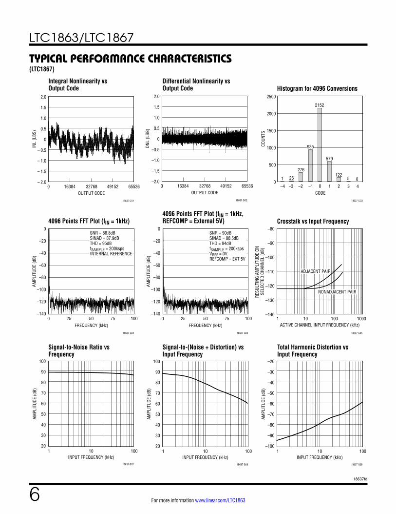
Integral Nonlinearity vs Output Code(LTC1867)
All registered trademarks and trademarks are the property of their respective owners.
LTC1863/LTC1867
218637fd
For more information www.linear.com/LTC1863
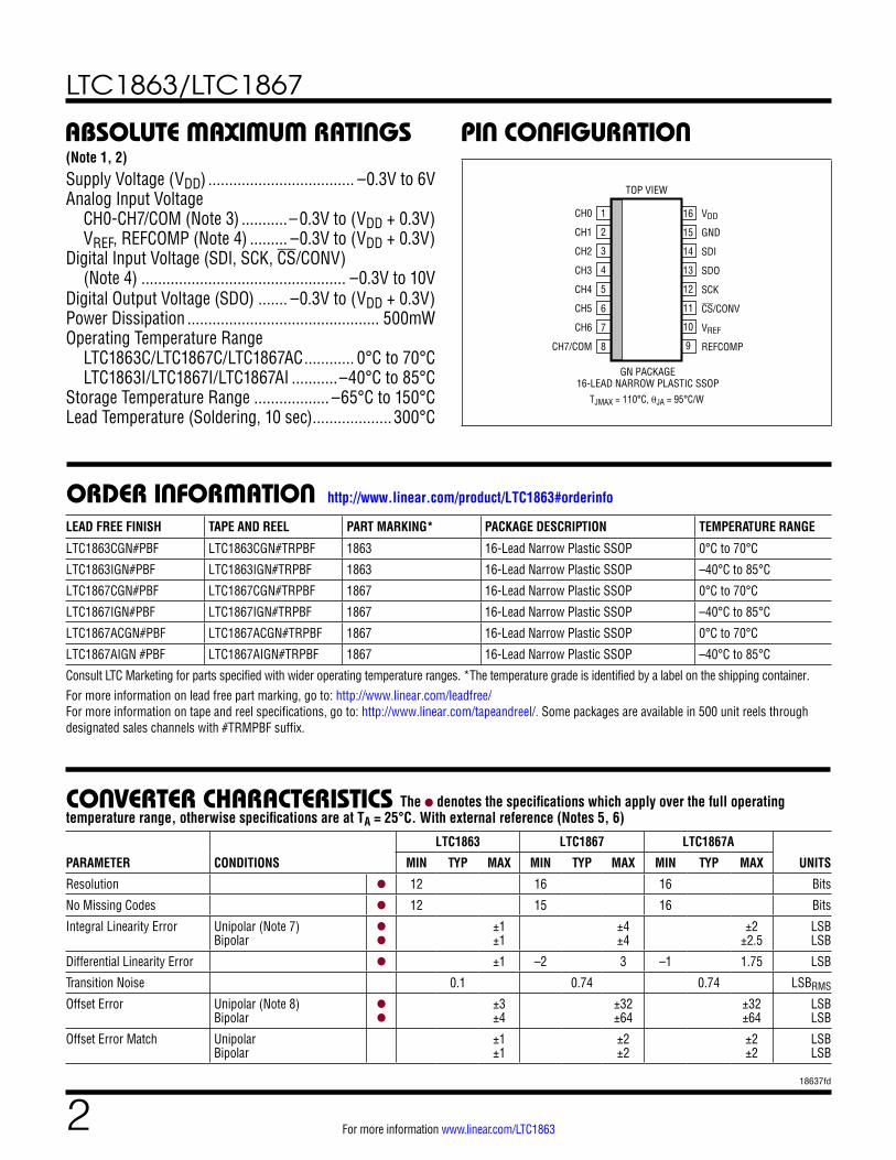
PIN CONFIGURATIONABSOLUTE MAXIMUM RATINGS(Note 1, 2)
TOP VIEW
GN PACKAGE16-LEAD NARROW PLASTIC SSOP
1
2
3
4
5
6
7
8
16
15
14
13
12
11
10
9
CH0
CH1
CH2
CH3
CH4
CH5
CH6
CH7/COM
VDD
GND
SDI
SDO
SCK
CS/CONV
VREF
REFCOMP
TJMAX = 110°C, θJA = 95°C/W
CONVERTER CHARACTERISTICS
ORDER INFORMATIONLEAD FREE FINISH TAPE AND REEL PART MARKING* PACKAGE DESCRIPTION TEMPERATURE RANGE
LTC1863CGN#PBF LTC1863CGN#TRPBF 1863 16-Lead Narrow Plastic SSOP 0°C to 70°C
LTC1863IGN#PBF LTC1863IGN#TRPBF 1863 16-Lead Narrow Plastic SSOP –40°C to 85°C
LTC1867CGN#PBF LTC1867CGN#TRPBF 1867 16-Lead Narrow Plastic SSOP 0°C to 70°C
LTC1867IGN#PBF LTC1867IGN#TRPBF 1867 16-Lead Narrow Plastic SSOP –40°C to 85°C
LTC1867ACGN#PBF LTC1867ACGN#TRPBF 1867 16-Lead Narrow Plastic SSOP 0°C to 70°C
LTC1867AIGN #PBF LTC1867AIGN#TRPBF 1867 16-Lead Narrow Plastic SSOP –40°C to 85°C
Consult LTC Marketing for parts specified with wider operating temperature ranges. *The temperature grade is identified by a label on the shipping container.For more information on lead free part marking, go to: http://www.linear.com/leadfree/ For more information on tape and reel specifications, go to: http://www.linear.com/tapeandreel/. Some packages are available in 500 unit reels through designated sales channels with #TRMPBF suffix.
Supply Voltage (VDD) ................................... –0.3V to 6VAnalog Input Voltage CH0-CH7/COM (Note 3) ...........–0.3V to (VDD + 0.3V) VREF, REFCOMP (Note 4) ......... –0.3V to (VDD + 0.3V)Digital Input Voltage (SDI, SCK, CS/CONV) (Note 4) ................................................. –0.3V to 10VDigital Output Voltage (SDO) ....... –0.3V to (VDD + 0.3V)Power Dissipation .............................................. 500mWOperating Temperature Range LTC1863C/LTC1867C/LTC1867AC ............ 0°C to 70°C LTC1863I/LTC1867I/LTC1867AI ...........–40°C to 85°CStorage Temperature Range .................. –65°C to 150°CLead Temperature (Soldering, 10 sec) ................... 300°C
The l denotes the specifications which apply over the full operating temperature range, otherwise specifications are at TA = 25°C. With external reference (Notes 5, 6)
PARAMETER CONDITIONS
LTC1863 LTC1867 LTC1867A
UNITSMIN TYP MAX MIN TYP MAX MIN TYP MAX
Resolution l 12 16 16 Bits
No Missing Codes l 12 15 16 Bits
Integral Linearity Error Unipolar (Note 7) Bipolar
l
l
±1 ±1
±4 ±4
±2 ±2.5
LSB LSB
Differential Linearity Error l ±1 –2 3 –1 1.75 LSB
Transition Noise 0.1 0.74 0.74 LSBRMS
Offset Error Unipolar (Note 8) Bipolar
l
l
±3 ±4
±32 ±64
±32 ±64
LSB LSB
Offset Error Match Unipolar Bipolar
±1 ±1
±2 ±2
±2 ±2
LSB LSB
http://www.linear.com/product/LTC1863#orderinfo
LTC1863/LTC1867
318637fd
For more information www.linear.com/LTC1863
SYMBOL PARAMETER CONDITIONS
LTC1863 LTC1867/LTC1867A
UNITSMIN TYP MAX MIN TYP MAX
SNR Signal-to-Noise Ratio 1kHz Input Signal 73.6 89 dB
S/(N+D) Signal-to-(Noise + Distortion) Ratio 1kHz Input Signal 73.5 88 dB
THD Total Harmonic Distortion 1kHz Input Signal, Up to 5th Harmonic –94.5 –95 dB
Peak Harmonic or Spurious Noise 1kHz Input Signal –94.5 –95 dB
Channel-to-Channel Isolation 100kHz Input Signal –100 –117 dB
Full Power Bandwidth –3dB Point 1.25 1.25 MHz
DYNAMIC ACCURACY
SYMBOL PARAMETER CONDITIONS
LTC1863/LTC1867/LTC1867A
UNITSMIN TYP MAX
Analog Input Range Unipolar Mode (Note 9) Bipolar Mode
l
l
0-4.096 ±2.048
V V
CIN Analog Input Capacitance for CH0 to CH7/COM
Between Conversions (Sample Mode) During Conversions (Hold Mode)
32 4
pF pF
tACQ Sample-and-Hold Acquisition Time l 1.5 1.1 µs
Input Leakage Current On Channels, CHX = 0V or VDD l ±1 µA
ANALOG INPUT The l denotes the specifications which apply over the full operating temperature range, otherwise specifications are at TA = 25°C. (Note 5)
PARAMETER CONDITIONS
LTC1863/LTC1867/LTC1867A
UNITSMIN TYP MAX
VREF Output Voltage IOUT = 0 2.48 2.5 2.52 V
VREF Output Tempco IOUT = 0 ±15 ppm/°C
VREF Line Regulation 4.75V ≤ VDD ≤ 5.25V 0.43 mV/V
VREF Output Resistance IOUT ≤0.1mA 6 kΩ
REFCOMP Output Voltage IOUT = 0 4.096 V
INTERNAL REFERENCE CHARACTERISTICS (Note 5)
CONVERTER CHARACTERISTICS The l denotes the specifications which apply over the full operating temperature range, otherwise specifications are at TA = 25°C. With external reference (Notes 5, 6)
PARAMETER CONDITIONS
LTC1863 LTC1867 LTC1867A
UNITSMIN TYP MAX MIN TYP MAX MIN TYP MAX
Offset Error Drift ±0.5 ±0.5 ±0.5 ppm/°C
Gain Error Unipolar Bipolar
±6 ±6
±96 ±96
±64 ±64
LSB LSB
Gain Error Match ±1 ±4 ±2 LSB
Gain Error Tempco Internal Reference External Reference
±15 ±2.7
±15 ±2.7
±15 ±2.7
ppm/°C ppm/°C
Power Supply Sensitivity VDD = 4.75V – 5.25V ±1 ±5 ±5 LSB
(Note 5)

LTC1863/LTC1867
418637fd
For more information www.linear.com/LTC1863
DIGITAL INPUTS AND DIGITAL OUTPUTS The l denotes the specifications which apply over the full operating temperature range, otherwise specifications are at TA = 25°C. (Note 5)
POWER REQUIREMENTS The l denotes the specifications which apply over the full operating temperature range, otherwise specifications are at TA = 25°C. (Note 5)
SYMBOL PARAMETER CONDITIONS
LTC1863/LTC1867/LTC1867A
UNITSMIN TYP MAX
VDD Supply Voltage (Note 9) 4.75 5.25 V
IDD Supply Current fSAMPLE = 200ksps NAP Mode SLEEP Mode
l
l
1.3 150 0.2
1.8 3
mA µA µA
PDISS Power Dissipation l 6.5 9 mW
SYMBOL PARAMETER CONDITIONS
LTC1863/LTC1867/LTC1867A
UNITSMIN TYP MAX
VIH High Level Input Voltage VDD = 5.25V l 2.4 V
VIL Low Level Input Voltage VDD = 4.75V l 0.8 V
IIN Digital Input Current VIN = 0V to VDD l ±10 µA
CIN Digital Input Capacitance 2 pF
VOH High Level Output Voltage (SDO) VDD = 4.75V, IO = –10µA VDD = 4.75V, IO = –200µA
l
44.75 4.74
V V
VOL Low Level Output Voltage (SDO) VDD = 4.75V, IO = 160µA VDD = 4.75V, IO = 1.6mA
l
0.05 0.1
0.4V V
ISOURCE Output Source Current SDO = 0V –32 mA
ISINK Output Sink Current SDO = VDD 19 mA
Hi-Z Output Leakage Hi-Z Output Capacitance
CS/CONV = High, SDO = 0V or VDD CS/CONV = High (Note 10)
l
l
±10 15
µA pF
Data Format Unipolar Bipolar
Straight Binary Two’s Complement
LTC1863/LTC1867
518637fd
For more information www.linear.com/LTC1863
TIMING CHARACTERISTICS
SYMBOL PARAMETER CONDITIONS
LTC1863/LTC1867/LTC1867A
UNITSMIN TYP MAX
fSAMPLE Maximum Sampling Frequency l 200 kHz
tCONV Conversion Time l 3 3.5 µs
tACQ Acquisition Time l 1.5 1.1 µs
fSCK SCK Frequency 40 MHz
t1 CS/CONV High Time Short CS/CONV Pulse Mode l 40 100 ns
t2 SDO Valid After SCK↓ CL = 25pF (Note 11) l 13 22 ns
t3 SDO Valid Hold Time After SCK↓ CL = 25pF l 5 11 ns
t4 SDO Valid After CS/CONV↓ CL = 25pF l 10 30 ns
t5 SDI Setup Time Before SCK↑ l 15 –6 ns
t6 SDI Hold Time After SCK↑ l 10 4 ns
t7 SLEEP Mode Wake-Up Time CREFCOMP = 10µF, CVREF = 2.2µF 60 ms
t8 Bus Relinquish Time After CS/CONV↑ CL = 25pF l 20 40 ns
Note 1: Stresses beyond those listed under Absolute Maximum Ratings may cause permanent damage to the device. Exposure to any Absolute Maximum Rating condition for extended periods may affect device reliability and lifetimeNote 2: All voltage values are with respect to GND (unless otherwise noted).Note 3: When these pin voltages are taken below GND or above VDD, they will be clamped by internal diodes. This product can handle input currents up to 100mA without latchup.Note 4: When these pin voltages are taken below GND, they will be clamped by internal diodes. This product can handle input currents up to 100mA below GND without latchup. These pins are not clamped to VDD.Note 5: VDD = 5V, fSAMPLE = 200ksps at 25°C, tr = tf = 5ns and VIN– = 2.5V for bipolar mode unless otherwise specified.Note 6: Linearity, offset and gain error specifications apply for both unipolar and bipolar modes. The INL and DNL are tested in bipolar mode.
Note 7: Integral nonlinearity is defined as the deviation of a code from a straight line passing through the actual endpoints of the transfer curve. The deviation is measured from the center of the quantization band.Note 8: Unipolar offset is the offset voltage measured from +1/2LSB when the output code flickers between 0000 0000 0000 0000 and 0000 0000 0000 0001 for LTC1867 and between 0000 0000 0000 and 0000 0000 0001 for LTC1863. Bipolar offset is the offset voltage measured from –1/2LSB when output code flickers between 0000 0000 0000 0000 and 1111 1111 1111 1111 for LTC1867, and between 0000 0000 0000 and 1111 1111 1111 for LTC1863. Note 9: Recommended operating conditions. The input range of ±2.048V for bipolar mode is measured with respect to VIN– = 2.5V.Note 10: Guaranteed by design, not subject to test.Note 11: t2 of 25ns maximum allows fSCK up to 20MHz for rising capture with 50% duty cycle and fSCK up to 40MHz for falling capture (with 3ns setup time for the receiving logic).
The l denotes the specifications which apply over the full operating temperature range, otherwise specifications are at TA = 25°C. (Note 5)
LTC1863/LTC1867
618637fd
For more information www.linear.com/LTC1863
Signal-to-Noise Ratio vs Frequency
Signal-to-(Noise + Distortion) vs Input Frequency
Total Harmonic Distortion vs Input Frequency
Integral Nonlinearity vs Output Code
Differential Nonlinearity vs Output Code Histogram for 4096 Conversions
4096 Points FFT Plot (fIN = 1kHz)4096 Points FFT Plot (fIN = 1kHz, REFCOMP = External 5V) Crosstalk vs Input Frequency
TYPICAL PERFORMANCE CHARACTERISTICS(LTC1867)
OUTPUT CODE0
INL
(LBS
)
49152
18637 GO1
16384 32768 65536
2.0
1.5
1.0
0.5
0
– 0.5
– 1.0
– 1.5
– 2.0
OUTPUT CODE0
DNL
(LSB
)
4915216384 32768 65536
2.0
1.5
1.0
0.5
0
–0.5
–1.0
–1.5
–2.0
18637 GO2
CODE–4
COUN
TS
4
18637 GO3
–2–3 0–1 321
2500
2000
1500
1000
500
01 26
276
2152
579
1225 0
935
FREQUENCY (kHz)0
0
–20
–40
–60
–80
–100
–120
–14075
18637 G04
25 50 100
AMPL
ITUD
E (d
B)
SNR = 88.8dBSINAD = 87.9dBTHD = 95dBfSAMPLE = 200kspsINTERNAL REFERENCE
FREQUENCY (kHz)0
0
–20
–40
–60
–80
–100
–120
–14075
18637 G05
25 50 100
AMPL
ITUD
E (d
B)
SNR = 90dBSINAD = 88.5dBTHD = 94dBfSAMPLE = 200kspsVREF = 0VREFCOMP = EXT 5V
ACTIVE CHANNEL INPUT FREQUENCY (kHz)1
RESU
LTIN
G AM
PLIT
UDE
ON
SELE
CTED
CHA
NNEL
(dB)
–80
–90
–100
–110
–120
–130
–14010 100 1000
18637 G06
ADJACENT PAIR
NONADJACENT PAIR
INPUT FREQUENCY (kHz)1
AMPL
ITUD
E (d
B)
100
90
80
70
60
50
40
30
2010 100
18637 G07
INPUT FREQUENCY (kHz)1
AMPL
ITUD
E (d
B)
100
90
80
70
60
50
40
30
2010 100
18637 G08
INPUT FREQUENCY (kHz)1
AMPL
ITUD
E (d
B)
–20
–30
–40
–50
–60
–70
–80
–90
–10010 100
18637 G09

LTC1863/LTC1867
718637fd
For more information www.linear.com/LTC1863
TYPICAL PERFORMANCE CHARACTERISTICS(LTC1863/LTC1867)
Supply Current vs fSAMPLE Supply Current vs Supply Voltage Supply Current vs Temperature
Differential Nonlinearity vs Output Code (LTC1863)
Integral Nonlinearity vs Output Code (LTC1863)
fSAMPLE (ksps)1
SUPP
LY C
URRE
NT (m
A)
2.0
1.5
1.0
0.5
010 100 1000
18637 G10
VDD = 5V
SUPPLY VOLTAGE (V)4.5
SUPP
LY C
URRE
NT (m
A)
5.5
18637 G11
4.75 5.0 5.25
1.5
1.4
1.3
1.2
1.1
1.0
VDD = 5VfSAMPLE = 200ksps
TEMPERATURE (°C)–50
SUPP
LY C
URRE
NT (m
A)
1.5
1.4
1.3
1.2
1.1
1.0–25 0 25 50
18637 G12
75 100
VDD = 5VfSAMPLE = 200ksps
OUTPUT CODE0
INL
(LBS
)
1.0
0.8
0.6
0.4
0.2
0
–0.2
–0.4
–0.6
–0.8
–1.01024 2048 2560
18637 G13
512 1536 3072 3584 4096OUTPUT CODE
0
DNL
(LBS
)
1.0
0.8
0.6
0.4
0.2
0
–0.2
–0.4
–0.6
–0.8
–1.01024 2048 2560
18637 G14
512 1536 3072 3584 4096
LTC1863/LTC1867
818637fd
For more information www.linear.com/LTC1863
PIN FUNCTIONS
TYPICAL CONNECTION DIAGRAM
TEST CIRCUITS
3k
(A) Hi-Z TO VOH AND VOL TO VOH
CL
3k
5V
DNDN
(B) Hi-Z TO VOL AND VOH TO VOL
CL
18637 TC01
3k
(A) VOH TO Hi-Z
CL
3k
5V
DNDN
(B) VOL TO Hi-Z
CL
18637 TC02
Load Circuits for Access Timing Load Circuits for Output Float Delay
LTC1863/LTC1867
–
+
+
DIGITALI/O
5V
4.096V10µF
2.2µF2.5V
±2.048V DIFFERENTIAL
INPUTS
4.096V SINGLE-ENDED
INPUT
18637 TCD
REFCOMP
VREF
CS/CONV
SCK
SDO
SDI
GND
VDD
CH7/COM
CH6CH5
CH4
CH3
CH2
CH1
CH0
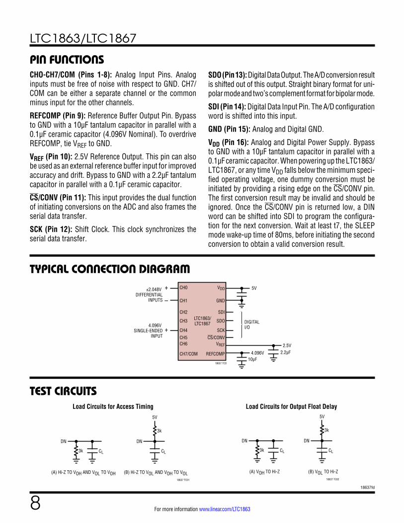
CHO-CH7/COM (Pins 1-8): Analog Input Pins. Analog inputs must be free of noise with respect to GND. CH7/COM can be either a separate channel or the common minus input for the other channels.
REFCOMP (Pin 9): Reference Buffer Output Pin. Bypass to GND with a 10µF tantalum capacitor in parallel with a 0.1µF ceramic capacitor (4.096V Nominal). To overdrive REFCOMP, tie VREF to GND.
VREF (Pin 10): 2.5V Reference Output. This pin can also be used as an external reference buffer input for improved accuracy and drift. Bypass to GND with a 2.2µF tantalum capacitor in parallel with a 0.1µF ceramic capacitor.
CS/CONV (Pin 11): This input provides the dual function of initiating conversions on the ADC and also frames the serial data transfer.
SCK (Pin 12): Shift Clock. This clock synchronizes the serial data transfer.
SDO (Pin 13): Digital Data Output. The A/D conversion result is shifted out of this output. Straight binary format for uni-polar mode and two’s complement format for bipolar mode.
SDI (Pin 14): Digital Data Input Pin. The A/D configuration word is shifted into this input.
GND (Pin 15): Analog and Digital GND.
VDD (Pin 16): Analog and Digital Power Supply. Bypass to GND with a 10µF tantalum capacitor in parallel with a 0.1µF ceramic capacitor. When powering up the LTC1863/LTC1867, or any time VDD falls below the minimum speci-fied operating voltage, one dummy conversion must be initiated by providing a rising edge on the CS/CONV pin. The first conversion result may be invalid and should be ignored. Once the CS/CONV pin is returned low, a DIN word can be shifted into SDI to program the configura-tion for the next conversion. Wait at least t7, the SLEEP mode wake-up time of 80ms, before initiating the second conversion to obtain a valid conversion result.

LTC1863/LTC1867
918637fd
For more information www.linear.com/LTC1863
TIMING DIAGRAMS
t5 (SDI Setup Time Before SCK↑), t6 (SDI Hold Time After SCK↑)
50%
50%
t3
0.4V
t7 (SLEEP Mode Wake-Up Time)t7
SCK
CS/CONV
t8 (BUS Relinquish Time)t8
CS/CONV
SDO
2.4V
t4 (SDO Valid After CONV↓)t4
CS/CONV
SDO2.4V
0.4V
0.4V
t6
2.4V0.4V
t5
SCK
SDI2.4V
2.4V
0.4V
2.4V0.4VSDO
1867 TD
SLEEP BIT (SLP = 0)READ-IN
10%
90% Hi-Z
Hi-Z
t1 (For Short Pulse Mode) t2 (SDO Valid Before SCK↑), t3 (SDO Valid Hold Time After SCK↓)t1
CS/CONV
t2
SCK50%50%
Overview
The LTC1863/LTC1867 are complete, low power multi-plexed ADCs. They consist of a 12-/16-bit, 200ksps capaci-tive successive approximation A/D converter, a precision internal reference, a configurable 8-channel analog input multiplexer (MUX) and a serial port for data transfer.
Conversions are started by a rising edge on the CS/CONV input. Once a conversion cycle has begun, it cannot be restarted. Between conversions, the ADCs receive an input word for channel selection and output the conversion result, and the analog input is acquired in preparation for the next conversion. In the acquire phase, a minimum time of 1.5µs will provide enough time for the sample-and-hold capacitors to acquire the analog signal.
During the conversion, the internal differential 16-bit capacitive DAC output is sequenced by the SAR from the most significant bit (MSB) to the least significant bit (LSB). The input is successively compared with the binary weighted charges supplied by the differential capacitive DAC. Bit decisions are made by a low-power, differential comparator. At the end of a conversion, the DAC output balances the analog input. The SAR contents (a 12-/16-bit data word) that represent the analog input are loaded into the 12-/16-bit output latches.
APPLICATIONS INFORMATION

LTC1863/LTC1867
1018637fd
For more information www.linear.com/LTC1863
APPLICATIONS INFORMATION
Examples of Multiplexer Options
CH0CH1CH2CH3CH4CH5CH6CH7/COM
GND (–)
8 Single-Ended
+++++++
4 Differential
+ (–) +
CH0CH1CH2CH3CH4CH5CH6
CH7/COM (–)
7 Single-Endedto CH7/COM
+++++++
+ (–)
+ (–)
+ (–)– (+)
– (+)
– (+)
– (+)
GND (–)
Combinations of Differential and Single-Ended
+++++
+––
{
{
{
{
{
{
18637 AI01
CH0CH1
CH2CH3
CH4CH5
CH6CH7/COM
CH0CH1
CH2CH3
CH4CH5CH6CH7/COM
Analog Input Multiplexer
The analog input multiplexer is controlled by a 7-bit input data word. The input data word is defined as follows:
SD OS S1 S0 COM UNI SLP
SD = SINGLE/DIFFERENTIAL BIT
OS = ODD/SIGN BIT
S1 = ADDRESS SELECT BIT 1
S0 = ADDRESS SELECT BIT 0
COM = CH7/COM CONFIGURATION BIT
UNI = UNIPOLAR/BIPOLAR BIT
SLP = SLEEP MODE BIT
Tables 1 and 2 show the configurations when COM = 0, and COM = 1.
Table 1. Channel Configuration (When COM = 0, CH7/COM Pin Is Used as CH7)
Channel ConfigurationSD OS S1 S0 COM “+” “–”
0 0 0 0 0 CH0 CH1
0 0 0 1 0 CH2 CH3
0 0 1 0 0 CH4 CH5
0 0 1 1 0 CH6 CH7
0 1 0 0 0 CH1 CH0
0 1 0 1 0 CH3 CH2
0 1 1 0 0 CH5 CH4
0 1 1 1 0 CH7 CH6
1 0 0 0 0 CH0 GND
1 0 0 1 0 CH2 GND
1 0 1 0 0 CH4 GND
1 0 1 1 0 CH6 GND
1 1 0 0 0 CH1 GND
1 1 0 1 0 CH3 GND
1 1 1 0 0 CH5 GND
1 1 1 1 0 CH7 GND
Table 2. Channel Configuration (When COM = 1, CH7/COM Pin Is Used as COMMON)
Channel Configuration
SD OS S1 S0 COM “+” “–”
1 0 0 0 1 CH0 CH7/COM
1 0 0 1 1 CH2 CH7/COM
1 0 1 0 1 CH4 CH7/COM
1 0 1 1 1 CH6 CH7/COM
1 1 0 0 1 CH1 CH7/COM
1 1 0 1 1 CH3 CH7/COM
1 1 1 0 1 CH5 CH7/COM
Changing the MUX Assignment “On the Fly”
CH7/COM (UNUSED)
CH7/COM (–)
1st Conversion 2nd Conversion
+–+–
+–
++
{
{
{
{
CH2CH3
CH4CH5
CH2CH3
CH4CH5
18637 AI02

LTC1863/LTC1867
1118637fd
For more information www.linear.com/LTC1863
Driving the Analog Inputs
The analog inputs of the LTC1863/LTC1867 are easy to drive. Each of the analog inputs can be used as a single-ended input relative to the GND pin (CH0-GND, CH1-GND, etc) or in pairs (CH0 and CH1, CH2 and CH3, CH4 and CH5, CH6 and CH7) for differential inputs. In addition, CH7 can act as a COM pin for both single-ended and differential modes if the COM bit in the input word is high. Regard-less of the MUX configuration, the “+” and “–” inputs are sampled at the same instant. Any unwanted signal that is common mode to both inputs will be reduced by the com-mon mode rejection of the sample-and-hold circuit. The inputs draw only one small current spike while charging the sample-and-hold capacitors during the acquire mode. In conversion mode, the analog inputs draw only a small leakage current. If the source impedance of the driving circuit is low then the LTC1863/LTC1867 inputs can be driven directly. More acquisition time should be allowed for a higher impedance source.
The following list is a summary of the op amps that are suitable for driving the LTC1863/LTC1867.
LT1007 - Low noise precision amplifier. 2.7mA supply current ±5V to ±15V supplies. Gain bandwidth product 8MHz. DC applications.
LT1097 - Low cost, low power precision amplifier. 300µA supply current. ±5V to ±15V supplies. Gain bandwidth product 0.7MHz. DC applications.
LT1227 - 140MHz video current feedback amplifier. 10mA supply current. ±5V to ±15V supplies. Low noise and low distortion.
LT1360 - 37MHz voltage feedback amplifier. 3.8mA supply current. ±5V to ±15V supplies. Good AC/DC specs.
LT1363 - 50MHz voltage feedback amplifier. 6.3mA supply current. Good AC/DC specs.
LT1364/LT1365 - Dual and quad 50MHz voltage feedback amplifiers. 6.3mA supply current per amplifier. Good AC/DC specs.
LT1468 - 90MHz, 22V/µs 16-bit accurate amplifier
LT1469 - Dual LT1468
Input Filtering
The noise and the distortion of the input amplifier and other circuitry must be considered since they will add to the LTC1863/LTC1867 noise and distortion. Noisy input circuitry should be filtered prior to the analog inputs to minimize noise. A simple 1-pole RC filter is sufficient for many applications. For instance, Figure 1 shows a 50Ω source resistor and a 2000pF capacitor to ground on the input will limit the input bandwidth to 1.6MHz. The source impedance has to be kept low to avoid gain error and degradation in the AC performance. The capacitor also acts as a charge reservoir for the input sample-and-hold and isolates the ADC input from sampling glitch sensitive circuitry. High quality capacitors and resistors should be used since these components can add distortion. NPO and silver mica type dielectric capacitors have excellent linearity. Carbon surface mount resistors can also generate distortion from self heating and from damage that may occur during soldering. Metal film surface mount resistors are much less susceptible to both problems.
APPLICATIONS INFORMATION
LTC1863/LTC1867
1218637fd
For more information www.linear.com/LTC1863
APPLICATIONS INFORMATION
DC Performance
One way of measuring the transition noise associated with a high resolution ADC is to use a technique where a DC signal is applied to the input of the ADC and the resulting output codes are collected over a large number of conversions. For example, in Figure 2 the distribution of output codes is shown for a DC input that had been digitized 4096 times. The distribution is Gaussian and the RMS code transition noise is about 0.74LSB.
1867 F01a
CH0
GND
LTC1863/LTC1867
REFCOMP
2000pF
10µF
50ΩANALOGINPUT
1000pF
1867 F01b
CH0
CH1
LTC1863/LTC1867
REFCOMP
1000pF
1000pF
10µF
50Ω
50Ω
DIFFERENTIALANALOGINPUTS
Figure 1a. Optional RC Input Filtering for Single-Ended Input
Figure 1b. Optional RC Input Filtering for Differential Inputs
Figure 2. LTC1867 Histogram for 4096 Conversions
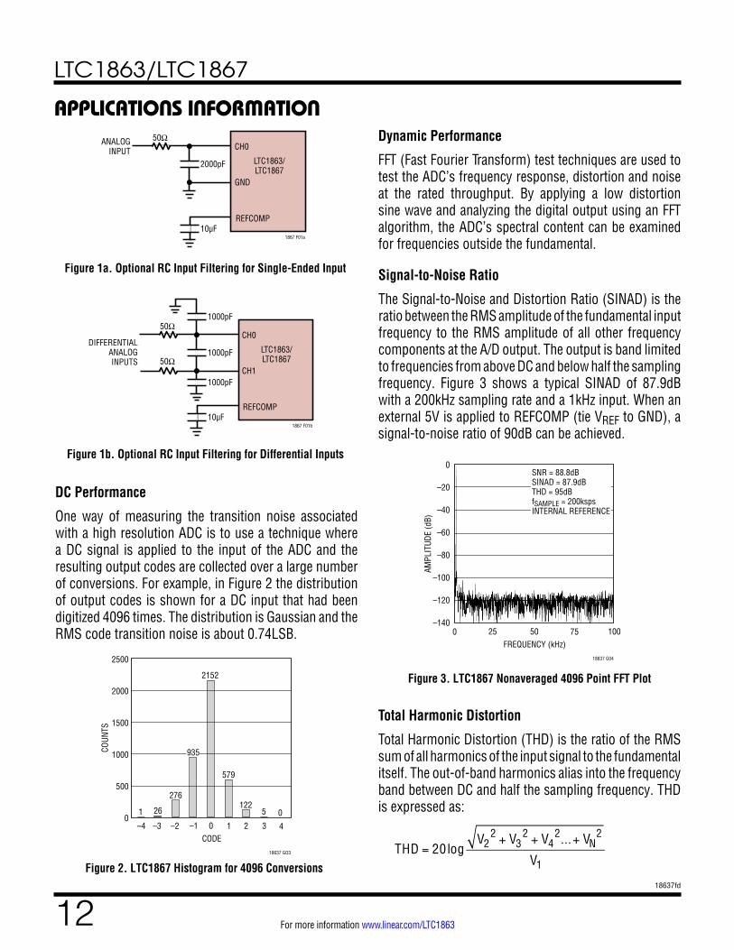
Dynamic Performance
FFT (Fast Fourier Transform) test techniques are used to test the ADC’s frequency response, distortion and noise at the rated throughput. By applying a low distortion sine wave and analyzing the digital output using an FFT algorithm, the ADC’s spectral content can be examined for frequencies outside the fundamental.
Signal-to-Noise Ratio
The Signal-to-Noise and Distortion Ratio (SINAD) is the ratio between the RMS amplitude of the fundamental input frequency to the RMS amplitude of all other frequency components at the A/D output. The output is band limited to frequencies from above DC and below half the sampling frequency. Figure 3 shows a typical SINAD of 87.9dB with a 200kHz sampling rate and a 1kHz input. When an external 5V is applied to REFCOMP (tie VREF to GND), a signal-to-noise ratio of 90dB can be achieved.
CODE–4
COUN
TS
4
18637 GO3
–2–3 0–1 321
2500
2000
1500
1000
500
01 26
276
2152
579
1225 0
935
Figure 3. LTC1867 Nonaveraged 4096 Point FFT Plot
FREQUENCY (kHz)0
0
–20
–40
–60
–80
–100
–120
–14075
18637 G04
25 50 100
AMPL
ITUD
E (d
B)
SNR = 88.8dBSINAD = 87.9dBTHD = 95dBfSAMPLE = 200kspsINTERNAL REFERENCE
Total Harmonic Distortion
Total Harmonic Distortion (THD) is the ratio of the RMS sum of all harmonics of the input signal to the fundamental itself. The out-of-band harmonics alias into the frequency band between DC and half the sampling frequency. THD is expressed as:
THD = 20log
V22 + V3
2 + V42...+ VN
2
V1

LTC1863/LTC1867
1318637fd
For more information www.linear.com/LTC1863
APPLICATIONS INFORMATIONDigital Interface
The LTC1863/LTC1867 have a very simple digital interface that is enabled by the control input, CS/CONV. A logic rising edge applied to the CS/CONV input will initiate a conversion. After the conversion, taking CS/CONV low will enable the serial port and the ADC will present digital data in two’s complement format in bipolar mode or straight binary format in unipolar mode, through the SCK/SDO serial port.
Internal Clock
The internal clock is factory trimmed to achieve a typical conversion time of 3µs and a maximum conversion time, 3.5µs, over the full operating temperature range. The typi-cal acquisition time is 1.1µs, and a throughput sampling rate of 200ksps is tested and guaranteed.
Automatic Nap Mode
The LTC1863/LTC1867 go into automatic nap mode when CS/CONV is held high after the conversion is complete (see Figure 6). With a typical operating current of 1.3mA and automatic 150µA nap mode between conversions, the power dissipation drops with reduced sample rate. The ADC only keeps the VREF and REFCOMP voltages active when the part is in the automatic nap mode. The slower the sample rate allows the power dissipation to be lower (see Figure 5).
R2
R3
REFERENCEAMP
10µF
2.2µF
REFCOMP
GND
VREF
R16k10
9
15
2.5V
4.096V
LTC1863/LTC1867
1867 F04a
BANDGAPREFERENCE
10
0.1µF10µF
1867 F04b
LT1019A-2.5VOUT
VIN
5V
VREF
LTC1863/LTC1867
GND
REFCOMP
15
9
+
2.2µF
Figure 4b. Using the LT1019-2.5 as an External Reference
Figure 4a. LTC1867 Reference Circuit
fSAMPLE (ksps)1
SUPP
LY C
URRE
NT (m
A)
2.0
1.5
1.0
0.5
010 100 1000
18637 G10
VDD = 5V
Figure 5. Supply Current vs fSAMPLE
where V1 is the RMS amplitude of the fundamental fre-quency and V2 through VN are the amplitudes of the second through Nth harmonics.
Internal Reference
The LTC1863/LTC1867 has an on-chip, temperature compensated, curvature corrected, bandgap reference that is factory trimmed to 2.5V. It is internally connected to a reference amplifier and is available at VREF (Pin 10). A 6k resistor is in series with the output so that it can be easily overdriven by an external reference if better drift and/or accuracy are required as shown in Figure 4. The reference amplifier gains the VREF voltage by 1.638V/V to 4.096V at REFCOMP (Pin 9). This reference amplifier compensation pin, REFCOMP, must be bypassed with a 10µF ceramic or tantalum in parallel with a 0.1µF ceramic for best noise performance.
LTC1863/LTC1867
1418637fd
For more information www.linear.com/LTC1863
APPLICATIONS INFORMATIONIf the CS/CONV returns low during a bit decision, it can create a small error. For best performance ensure that the CS/CONV returns low either within 100ns after the conversion starts (i.e. before the first bit decision) or after the conversion ends. If CS/CONV is low when the conversion ends, the MSB bit will appear on SDO at the end of the conversion and the ADC will remain powered up (see Figure 7).
Sleep Mode
If the SLP = 1 is selected in the input word, the ADC will enter SLEEP mode and draw only leakage current (provided that all the digital inputs stay at GND or VDD). After release from the SLEEP mode, the ADC need 60ms to wake up (2.2µF/10µF bypass capacitors on VREF/ REFCOMP pins).
Board Layout and Bypassing
To obtain the best performance, a printed circuit board with a ground plane is required. Layout for the printed circuit board should ensure digital and analog signal lines are separated as much as possible. In particular, care should be taken not to run any digital signal alongside an analog signal.
All analog inputs should be screened by GND. VREF, REFCOMP and VDD should be bypassed to this ground plane as close to the pin as possible; the low impedance
of the common return for these bypass capacitors is es-sential to the low noise operation of the ADC. The width for these tracks should be as wide as possible.
Timing and Control
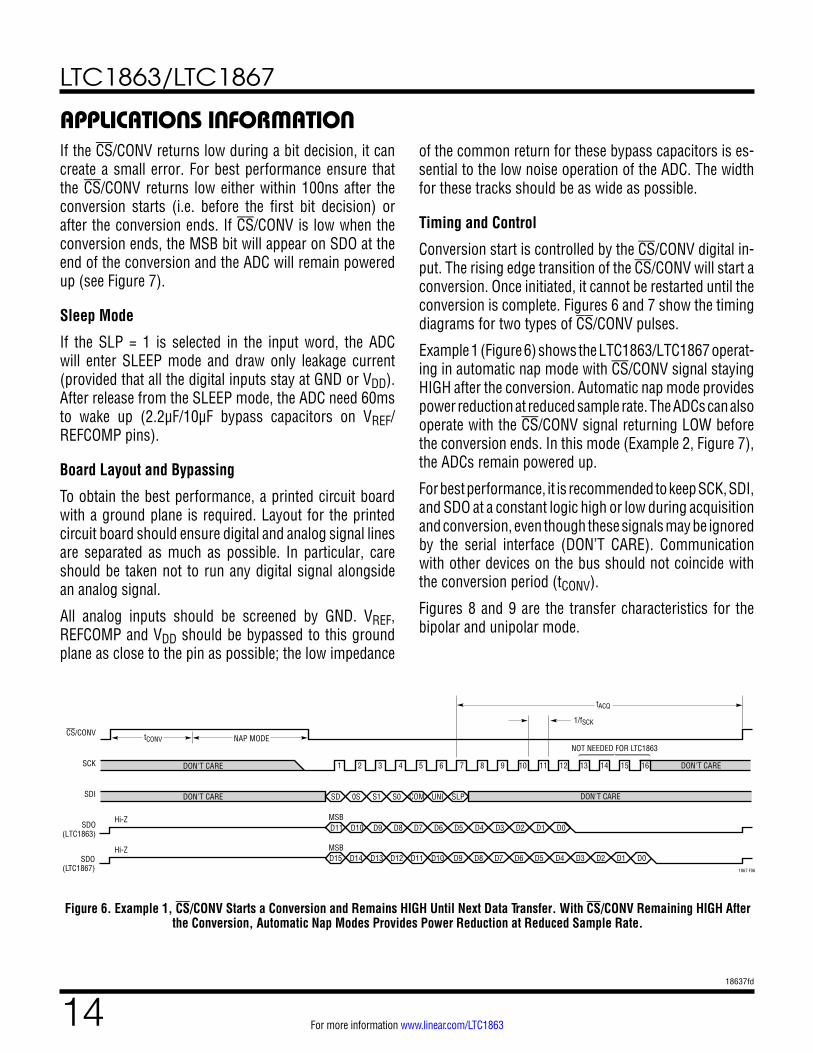
Conversion start is controlled by the CS/CONV digital in-put. The rising edge transition of the CS/CONV will start a conversion. Once initiated, it cannot be restarted until the conversion is complete. Figures 6 and 7 show the timing diagrams for two types of CS/CONV pulses.
Example 1 (Figure 6) shows the LTC1863/LTC1867 operat-ing in automatic nap mode with CS/CONV signal staying HIGH after the conversion. Automatic nap mode provides power reduction at reduced sample rate. The ADCs can also operate with the CS/CONV signal returning LOW before the conversion ends. In this mode (Example 2, Figure 7), the ADCs remain powered up.
For best performance, it is recommended to keep SCK, SDI, and SDO at a constant logic high or low during acquisition and conversion, even though these signals may be ignored by the serial interface (DON’T CARE). Communication with other devices on the bus should not coincide with the conversion period (tCONV).
Figures 8 and 9 are the transfer characteristics for the bipolar and unipolar mode.
S0SD 0S S1 COM UNI SLP
D11 D10 D9 D8 D7 D6 D5 D4 D3 D2 D1 D0
1/fSCK
tACQ
CS/CONV
SCK
SDI
SDO(LTC1863)
Hi-Z
D12D15 D14 D13 D11 D10 D9 D8 D7 D6 D5 D4 D3 D2 D1 D0Hi-Z
1 2 3 4 5 6 7 8 9 10 11 12 13 14 15 16
1867 F06
DON'T CARE
NOT NEEDED FOR LTC1863tCONV NAP MODE
SDO(LTC1867)
MSB
MSB
DON'T CAREDON'T CARE
DON'T CARE
Figure 6. Example 1, CS/CONV Starts a Conversion and Remains HIGH Until Next Data Transfer. With CS/CONV Remaining HIGH After the Conversion, Automatic Nap Modes Provides Power Reduction at Reduced Sample Rate.

LTC1863/LTC1867
1518637fd
For more information www.linear.com/LTC1863
Figure 7. Example 2, CS/CONV Starts a Conversion With Short Active HIGH Pulse. With CS/CONV Returning LOW Before the Conversion, the ADC Remains Powered Up.
INPUT VOLTAGE (V)
OUTP
UT C
ODE
1867 F09
111...111
111...110
100...001
100...000
000...000
000...001
011...110
011...111
FS – 1LSB0V
UNIPOLARZERO
FS = 4.0961LSB = FS/2n
1LSB = (LTC1863) = 1mV1LSB = (LTC1867) = 62.5µV
Figure 8. LTC1863/LTC1867 Bipolar Transfer Characteristics (Two’s Complement)
Figure 9. LTC1863/LTC1867 Unipolar Transfer Characteristics (Straight Binary)
S0SD 0S S1 COM UNI SLP
MSB = D11 D10 D9 D8 D7 D6 D5 D4 D3 D2 D1 D0
CS/CONV
SCK
SDI
SDO(LTC1867)
Hi-Z
1 2 3 4 5 6 7 8 9 10 11 12 13 14 15 16
tCONV
D12MSB = D15 D14 D13 D11 D10 D9 D8 D7 D6 D5 D4 D3 D2 D1 D0Hi-Z 1867 F07
tCONV
DON'T CAREDON'T CARE
NOT NEEDED FOR LTC1863
tACQ
SDO(LTC1863)
DON'T CARE
INPUT VOLTAGE (V)
0V
OUTP
UT C
ODE
(TW
O’S
COM
PLEM
ENT)
–1 LSB
1867 F08
011...111
011...110
000...001
000...000
100...000
100...001
111...110
1LSB
BIPOLARZERO
111...111
FS/2 – 1LSB–FS/2
FS = 4.0961LSB = FS/2n
1LSB = (LTC1863) = 1mV1LSB = (LTC1867) = 62.5µV
APPLICATIONS INFORMATION

LTC1863/LTC1867
1618637fd
For more information www.linear.com/LTC1863
PACKAGE DESCRIPTION
GN Package16-Lead Plastic SSOP (Narrow .150 Inch)
(Reference LTC DWG # 05-08-1641 Rev B)
GN16 REV B 0212
1 2 3 4 5 6 7 8
.229 – .244(5.817 – 6.198)
.150 – .157**(3.810 – 3.988)
16 15 14 13
.189 – .196*(4.801 – 4.978)
12 11 10 9
.016 – .050(0.406 – 1.270)
.015 ±.004(0.38 ±0.10)
× 45°
0° – 8° TYP.007 – .0098(0.178 – 0.249)
.0532 – .0688(1.35 – 1.75)
.008 – .012(0.203 – 0.305)
TYP
.004 – .0098(0.102 – 0.249)
.0250(0.635)
BSC
.009(0.229)
REF
.254 MIN
RECOMMENDED SOLDER PAD LAYOUT
.150 – .165
.0250 BSC.0165 ±.0015
.045 ±.005
* DIMENSION DOES NOT INCLUDE MOLD FLASH. MOLD FLASH SHALL NOT EXCEED 0.006" (0.152mm) PER SIDE** DIMENSION DOES NOT INCLUDE INTERLEAD FLASH. INTERLEAD FLASH SHALL NOT EXCEED 0.010" (0.254mm) PER SIDE
INCHES(MILLIMETERS)
NOTE:1. CONTROLLING DIMENSION: INCHES
2. DIMENSIONS ARE IN
3. DRAWING NOT TO SCALE4. PIN 1 CAN BE BEVEL EDGE OR A DIMPLE
GN Package16-Lead Plastic SSOP (Narrow .150 Inch)
(Reference LTC DWG # 05-08-1641 Rev B)
Please refer to http://www.linear.com/product/LTC1863#packaging for the most recent package drawings.

LTC1863/LTC1867
1718637fd
For more information www.linear.com/LTC1863
Information furnished by Analog Devices is believed to be accurate and reliable. However, no responsibility is assumed by Analog Devices for its use, nor for any infringements of patents or other rights of third parties that may result from its use. Specifications subject to change without notice. No license is granted by implication or otherwise under any patent or patent rights of Analog Devices.
REVISION HISTORYREV DATE DESCRIPTION PAGE NUMBER
B 6/14 Fixed the Order Information. 2
C 5/15 Adjusted Notes 3 and 4 to specify input currents up to 100mA. 5
D 2/18 Added dummy conversion requirement on power up to VDD pin description 8

LTC1863/LTC1867
1818637fd
For more information www.linear.com/LTC1863 LINEAR TECHNOLOGY CORPORATION 2008
LT 0218 REV D • PRINTED IN USAwww.linear.com/LTC1863
RELATED PARTSPART NUMBER DESCRIPTION COMMENTS
LTC1417 14-Bit, 400ksps Serial ADC 20mW, Unipolar or Bipolar, Internal Reference, SSOP-16 Package
LT1460 Micropower Precision Series Reference Bandgap, 130µA Supply Current, 10ppm/°C, SOT-23 Package
LT1468/LT1469 Single/Dual 90MHz, 22V/µs, 16-Bit Accurate Op Amps Low Input Offset: 75µV/125µV
LTC1609 16-Bit, 200ksps Serial ADC 65mW, Configurable Bipolar and Unipolar Input Ranges, 5V Supply
LT1790 Micropower Low Dropout Reference 60µA Supply Current, 10ppm/°C, SOT-23 Package
LTC1850/LTC1851 10-Bit/12-Bit, 8-Channel, 1.25Msps ADC Parallel Output, Programmable MUX and Sequencer, 5V Supply
LTC1852/LTC1853 10-Bit/12-Bit, 8-Channel, 400ksps ADC Parallel Output, Programmable MUX and Sequencer, 3V or 5V Supply
LTC1860/LTC1861 12-Bit, 1-/2-Channel 250ksps ADC in MSOP 850µA at 250ksps, 2µA at 1ksps, SO-8 and MSOP Packages
LTC1860L/LTC1861L 3V, 12-Bit, 1-/2-Channel 150ksps ADC 450µA at 150ksps, 10µA at 1ksps, SO-8 and MSOP Packages
LTC1864/LTC1865 16-Bit, 1-/2-Channel 250ksps ADC in MSOP 850µA at 250ksps, 2µA at 1ksps, SO-8 and MSOP Packages
LTC1864L/LTC1865L 3V, 16-Bit, 1-/2-Channel 150ksps ADC in MSOP 450µA at 150ksps, 10µA at 1ksps, SO-8 and MSOP Packages