lsr sterling-lwb wi-fi & bluetooth module datasheet · sterling-lwb module datasheet ... o easy...
TRANSCRIPT
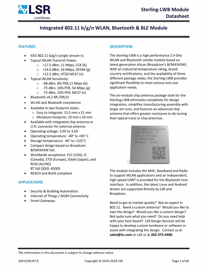
Sterling-LWB Module
Datasheet
The information in this document is subject to change without notice. 330-0190-R7.0 Copyright © 2016-2018 LSR Page 1 of 66
Integrated 802.11 b/g/n WLAN, Bluetooth & BLE Module
FEATURES
• IEEE 802.11 b/g/n (single stream n)
• Typical WLAN Transmit Power: o +17.5 dBm, 11 Mbps, CCK (b) o +14.0 dBm, 54 Mbps, OFDM (g) o +12.5 dBm, HT20 MCS7 (n)
• Typical WLAN Sensitivity: o -88 dBm, 8% PER,11 Mbps (b) o -75 dBm, 10% PER, 54 Mbps (g) o -72 dBm, 10% PER, MCS7 (n)
• Bluetooth v4.2 BR /DR/LE
• WLAN and Bluetooth coexistence
• Available in two footprint styles: o Easy to Integrate: 15.5 mm x 21 mm o Miniature footprint: 10 mm x 10 mm
• Available with integrated chip antenna or U.FL connector for external antenna
• Operating voltage: 3.0V to 3.6V
• Operating temperature: -40o to +85o C
• Storage temperature: -40° to +125°C
• Compact design based on Broadcom BCM4343W SoC
• Worldwide acceptance: FCC (USA), IC (Canada), ETSI (Europe), Giteki (Japan), and RCM (AU/NZ) BT SIG QDID: 85005
• REACH and RoHS compliant
APPLICATIONS
• Security & Building Automation
• Internet of Things / M2M Connectivity
• Smart Gateways
DESCRIPTION
The Sterling-LWB is a high performance 2.4 GHz WLAN and Bluetooth combo module based on latest-generation silicon (Broadcom’s BCM4343W). With an industrial temperature rating, broad country certifications, and the availability of three different package styles, the Sterling-LWB provides significant flexibility to meet various end user application needs.
The on-module chip antenna package style for the Sterling-LWB eliminates complexity for design integration, simplifies manufacturing assembly with larger pin outs, and features an advanced chip antenna that offers greater resistance to de-tuning than typical trace or chip antennas.
The module includes the MAC, Baseband and Radio to support WLAN applications and an independent, high-speed UART is provided for the Bluetooth host interface. In addition, the latest Linux and Android drivers are supported directly by LSR and Broadcom. Need to get to market quickly? Not an expert in 802.11. Need a custom antenna? Would you like to own the design? Would you like a custom design? Not quite sure what you need? Do you need help with your host board? LSR Design Services will be happy to develop custom hardware or software or assist with integrating the design. Contact us at [email protected] or call us at 262-375-4400.

Sterling-LWB Module
Datasheet
The information in this document is subject to change without notice. 330-0190-R7.0 Copyright © 2016-2018 LSR Page 2 of 66
TABLE OF CONTENTS
FEATURES ................................................................................................................................... 1
APPLICATIONS ............................................................................................................................ 1
DESCRIPTION .............................................................................................................................. 1
TABLE OF CONTENTS ................................................................................................................... 2
MODULE VARIANTS .................................................................................................................... 5
FUNCTIONAL FEATURES .............................................................................................................. 8
WLAN Features ...................................................................................................................................................... 8
Bluetooth Features ................................................................................................................................................ 8
Wireless Security System Features ........................................................................................................................ 8
ORDERING INFORMATION .......................................................................................................... 9
MODULE ACCESSORIES ................................................................................................................ 9
APPLICABLE DOCUMENTS ......................................................................................................... 10
BLOCK DIAGRAMS ..................................................................................................................... 11
BASE SIP MODULE FOOTPRINT AND PIN DEFINITIONS ............................................................... 14
BASE SIP MODULE PIN DESCRIPTIONS ....................................................................................... 15
U.FL AND CHIP ANTENNA MODULE FOOTPRINT AND PIN DEFINITIONS ...................................... 20
U.FL AND CHIP ANTENNA MODULE PIN DESCRIPTIONS .............................................................. 21
MODULE POWER STATES .......................................................................................................... 23
U.FL AND CHIP ANTENNA MODULE PIN I/O STATES ................................................................... 24
GENERAL CHARACTERISTICS ...................................................................................................... 27
WLAN Power Consumption.................................................................................................................................. 29
Bluetooth Power Consumption ............................................................................................................................ 29
Power Supply Requirements ................................................................................................................................ 30
Calibration Current Profile ................................................................................................................................... 31
CRYSTAL OSCILLATOR REQUIREMENTS ...................................................................................... 32

Sterling-LWB Module
Datasheet
The information in this document is subject to change without notice. 330-0190-R7.0 Copyright © 2016-2018 LSR Page 3 of 66
CONTROL SIGNAL TIMING DIAGRAMS ....................................................................................... 33
WLAN RF Characteristics ...................................................................................................................................... 35
Bluetooth RF Characteristics ................................................................................................................................ 37
WLAN HOST INTERFACE ............................................................................................................ 38
SDIO Interface ..................................................................................................................................................... 38
BLUETOOTH UART HOST INTERFACE .......................................................................................... 40
Overview ............................................................................................................................................................. 40
Soldering Recommendations ............................................................................................................................... 41
Recommended Reflow Profile for Lead Free Solder ............................................................................................. 41
WIFI MAC IDS/BLUETOOTH MAC IDS ......................................................................................... 42
CLEANING ................................................................................................................................. 43
OPTICAL INSPECTION ................................................................................................................ 43
REWORK ................................................................................................................................... 43
SHIPPING, HANDLING, AND STORAGE ....................................................................................... 43
Shipping ............................................................................................................................................................... 43
Handling .............................................................................................................................................................. 43
Moisture Sensitivity Level (MSL) .......................................................................................................................... 43
Storage ................................................................................................................................................................ 43
Repeated Reflow Soldering .................................................................................................................................. 44
AGENCY CERTIFICATIONS .......................................................................................................... 45
AGENCY STATEMENTS ............................................................................................................... 45
Federal Communication Commission Interference Statement ............................................................................. 45
Industry Canada Statements ................................................................................................................................ 46
OEM RESPONSIBILITIES TO COMPLY WITH FCC AND INDUSTRY CANADA REGULATIONS ............. 47
OEM LABELING REQUIREMENTS FOR END-PRODUCT ................................................................. 48
OEM END PRODUCT USER MANUAL STATEMENTS ..................................................................... 49
EUROPE .................................................................................................................................... 50
CE Notice ............................................................................................................................................................. 50
Declaration of Conformity (DOC) ......................................................................................................................... 50
Sterling-LWB Module
Datasheet
The information in this document is subject to change without notice. 330-0190-R7.0 Copyright © 2016-2018 LSR Page 4 of 66
AUSTRALIA ............................................................................................................................... 50
RCM ..................................................................................................................................................................... 50
BLUETOOTH SIG QUALIFICATION ............................................................................................... 51
Overview ............................................................................................................................................................. 51
Qualification Steps When Referencing a Laird Controller Subsystem Design ....................................................... 51
Additional Assistance........................................................................................................................................... 52
BASE SIP MODULE MECHANICAL DATA ...................................................................................... 53
BASE SIP MODULE PCB FOOTPRINT ........................................................................................... 54
BASE SIP MODULE RECOMMENDED SOLDER STENCIL ................................................................ 55
BASE SIP MODULE TAPE AND REEL PACKAGING ......................................................................... 56
U.FL AND CHIP ANTENNA MECHANICAL DATA ........................................................................... 57
U.FL AND CHIP ANTENNA PCB FOOTPRINT ................................................................................ 58
U.FL AND CHIP ANTENNA TAPE AND REEL PACKAGING .............................................................. 59
DEVICE MARKINGS .................................................................................................................... 60
SiP Module .......................................................................................................................................................... 60
Antenna Option Modules .................................................................................................................................... 62
CONTACTING LSR ...................................................................................................................... 66

Sterling-LWB Module
Datasheet
The information in this document is subject to change without notice. 330-0190-R7.0 Copyright © 2016-2018 LSR Page 5 of 66
MODULE VARIANTS
The LSR Sterling-LWB Module is available in three different versions. Depending on the user’s antenna and footprint needs, there is a variant to suite most application requirements. LSR recommends that for simplicity of both the host PCB design, as well as the manufacturing process, that either the Chip Antenna or RF Connector version of the modules be used in your design.
• 450-0159 - Base SiP Module This module variant is supplied in a compact, 151 pin, 0.5 mm pitch LGA footprint. Unlike the other module variants, it requires the addition of either an off module antenna or RF connector, as well as the associated matching components. In order to benefit from the EMC certifications on the module, strictly following the layout in the module application guide is required. This requires adherence to the PCB stack-up and layout around the antenna. The footprint of this module may require additional care during reflow and PCB assembly.
Figure 1 Sterling-LWB Base SiP Module (450-0159)

Sterling-LWB Module
Datasheet
The information in this document is subject to change without notice. 330-0190-R7.0 Copyright © 2016-2018 LSR Page 6 of 66
• 450-0148 – U.FL Module This module variant integrates the 450-0159 Base SiP Module, a U.FL RF connector, and all associated RF matching components on a PCB. This integrated approach not only provides a U.FL connector for connections to external antennas, but also simplifies and reduces the cost of the end users host board by simplifying the module PCB footprint.
Figure 2 Sterling-LWB U.FL Module (450-0148)

Sterling-LWB Module
Datasheet
The information in this document is subject to change without notice. 330-0190-R7.0 Copyright © 2016-2018 LSR Page 7 of 66
• 450-0152 - Chip Antenna Module This module variant integrates the 450-0159 Base SiP Module, a chip antenna, and all associated RF matching components on a PCB. This integrated approach not only provides an external antenna solution, but also simplifies and reduces the cost of the end users host board by simplifying the module PCB footprint.
Figure 3 Sterling-LWB Chip Antenna Module (450-0152)

Sterling-LWB Module
Datasheet
The information in this document is subject to change without notice. 330-0190-R7.0 Copyright © 2016-2018 LSR Page 8 of 66
FUNCTIONAL FEATURES
WLAN Features
• IEEE802.11b/g/n 1x1 2.4 GHz Radio o Internal Power Amplifier (PA) o Internal Low Noise Amplifier(LNA) o Internal T/R Switch o Simultaneous BT/WLAN reception with a single antenna.
• Media Access Controller (MAC)
• Physical Layer (PHY)
• Baseband Processor
• Standards o IEEE 802.11b, 802.11g, 802.11n (single stream)
Bluetooth Features
• Class 2 power amplifier with Class 2 capability
• HCI Interface using High Speed UART
• PCM for Audio Data
• Bluetooth v4.2 BR /DR/LE
Wireless Security System Features
• Supported modes: o Open (no security) o WEP o WPA Personal o WPA2 Personal o WMM o WMM-PS (U-APSD) o WMM-SA o WAPI o AES (Hardware Accelerator) o TKIP (host-computed) o CKIP (SW Support)

Sterling-LWB Module
Datasheet
The information in this document is subject to change without notice. 330-0190-R7.0 Copyright © 2016-2018 LSR Page 9 of 66
ORDERING INFORMATION
Order Number Description
450-0148C Sterling-LWB U.FL Module (Cut Tape)
450-0148R Sterling-LWB U.FL Module (Tape and Reel, SPQ = 1000)
450-0152C Sterling-LWB Chip Antenna Module (Cut Tape)
450-0152R Sterling-LWB Chip Antenna Module (Tape and Reel, SPQ = 1000)
450-0159C Sterling-LWB Base SiP Module (Cut Tape)
450-0159R Sterling-LWB Base SiP Module (Tape and Reel, SPQ = 1000)
450-0155 Sterling-LWB SD Development Board, U.FL
450-0156 Sterling-LWB SD Development Board, Chip Antenna
450-0173 Sterling-LWB Development Board, WICED
Table 1 Orderable Sterling-LWB Part Numbers
MODULE ACCESSORIES
Order Number Description
001-0001 2.4 GHz Dipole Antenna with Reverse Polarity
SMA Connector
080-0001 U.FL to Reverse Polarity SMA Bulkhead Cable
105mm
Sterling-LWB Module
Datasheet
The information in this document is subject to change without notice. 330-0190-R7.0 Copyright © 2016-2018 LSR Page 10 of 66
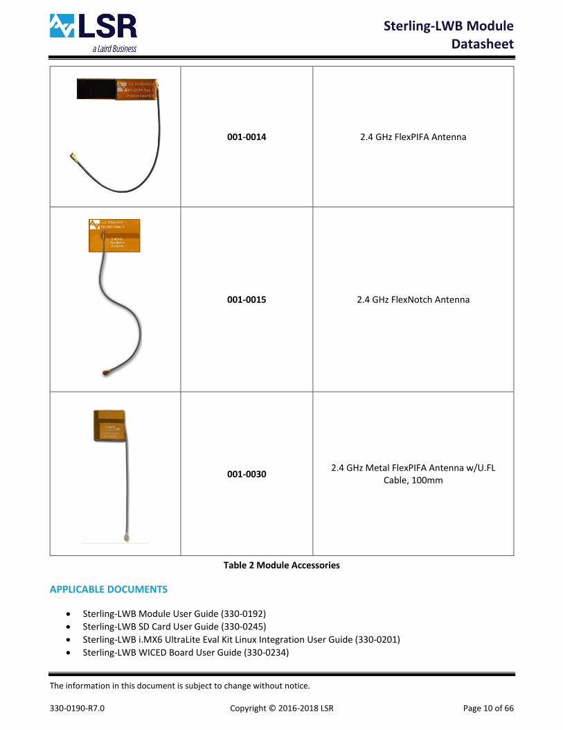
001-0014 2.4 GHz FlexPIFA Antenna
001-0015 2.4 GHz FlexNotch Antenna
001-0030 2.4 GHz Metal FlexPIFA Antenna w/U.FL
Cable, 100mm
Table 2 Module Accessories
APPLICABLE DOCUMENTS
• Sterling-LWB Module User Guide (330-0192)
• Sterling-LWB SD Card User Guide (330-0245)
• Sterling-LWB i.MX6 UltraLite Eval Kit Linux Integration User Guide (330-0201)
• Sterling-LWB WICED Board User Guide (330-0234)

Sterling-LWB Module
Datasheet
The information in this document is subject to change without notice. 330-0190-R7.0 Copyright © 2016-2018 LSR Page 11 of 66
BLOCK DIAGRAMS
Figure 4 Sterling-LWB Base SiP Module Block Diagram

Sterling-LWB Module
Datasheet
The information in this document is subject to change without notice. 330-0190-R7.0 Copyright © 2016-2018 LSR Page 12 of 66
Figure 5 Sterling-LWB U.FL Module Block Diagram

Sterling-LWB Module
Datasheet
The information in this document is subject to change without notice. 330-0190-R7.0 Copyright © 2016-2018 LSR Page 13 of 66
Figure 6 Sterling-LWB Chip Antenna Module Block Diagram

Sterling-LWB Module
Datasheet
The information in this document is subject to change without notice. 330-0190-R7.0 Copyright © 2016-2018 LSR Page 14 of 66
BASE SIP MODULE FOOTPRINT AND PIN DEFINITIONS
Note that the following footprint and pin definition applies to the Sterling-LWB Base SiP Module (450-0159). There are two module footprints depending on which variant of the module is being used, so it is important to make certain you are using the correct version on your design.
Figure 7 Sterling-LWB Base SiP Module Pinout (Top View)

Sterling-LWB Module
Datasheet
The information in this document is subject to change without notice. 330-0190-R7.0 Copyright © 2016-2018 LSR Page 15 of 66
BASE SIP MODULE PIN DESCRIPTIONS
Module Pin
Name I/O Type Description
1 ANT RF RF TRANSMITTER OUTPUT AND RECEIVE INPUT
2 GND GND GROUND
3 VDD_3V3_WIFI_PA PI WIFI PA POWER SUPPLY
4 VDD_3V3_WIFI_PA PI WIFI PA POWER SUPPLY
5 GND GND GROUND
6 NC - NO CONNECT (DO NOT CONNECT)
7 GND GND GROUND
8 NC - NO CONNECT (DO NOT CONNECT)
9 NC - NO CONNECT (DO NOT CONNECT)
10 GND GND GROUND
11 NC - NO CONNECT (DO NOT CONNECT)
12 NC - NO CONNECT (DO NOT CONNECT)
13 NC - NO CONNECT (DO NOT CONNECT)
14 NC - NO CONNECT (DO NOT CONNECT)
15 GND GND GROUND
16 NC - NO CONNECT (DO NOT CONNECT)
17 NC - NO CONNECT (DO NOT CONNECT)
18 GND GND GROUND
19 CLK_REQ DO EXTERNAL SYSTEM CLOCK REQUEST – USED WHEN THE SYSTEM CLOCK IS NOT PROVIDED BY A DEDICATED CRYSTAL
20 BT_GPIO_3 DIO WPT_INTb TO WIRELESS CHARGING PMU
21 NC - NO CONNECT (DO NOT CONNECT)
22 NC - NO CONNECT (DO NOT CONNECT)
23 GND GND GROUND
24 NC - NO CONNECT (DO NOT CONNECT)
25 GND GND GROUND
26 32K_PWM_IN DI EXTERNAL SLEEP CLOCK INPUT
27 GND GND GROUND
28 VDD3V3_WiFi_IO PI DC SUPPY FOR WIFI AND I/O
29 GND GND GROUND
30 NC - NO CONNECT (DO NOT CONNECT)

Sterling-LWB Module
Datasheet
The information in this document is subject to change without notice. 330-0190-R7.0 Copyright © 2016-2018 LSR Page 16 of 66
Module Pin
Name I/O Type Description
31 NC - NO CONNECT (DO NOT CONNECT)
32 NC - NO CONNECT (DO NOT CONNECT)
33 NC - NO CONNECT (DO NOT CONNECT)
34 GND GND GROUND
35 NC - NO CONNECT (DO NOT CONNECT)
36 GND GND GROUND
37 NC - NO CONNECT (DO NOT CONNECT)
38 NC - NO CONNECT (DO NOT CONNECT)
39 GND GND GROUND
40 SDIO_D3 DIO SDIO DATA LINE 3
41 GND GND GROUND
42 VDD3V3_WIFI PI WIFI POWER SUPPLY
43 VDD3V3_WIFI PI WIFI POWER SUPPLY
44 GND GND GROUND
45 NC - NO CONNECT (DO NOT CONNECT)
46 NC - NO CONNECT (DO NOT CONNECT)
47 GND GND GROUND
48 NC - NO CONNECT (DO NOT CONNECT)
49 GND GND GROUND
50 NC - NO CONNECT (DO NOT CONNECT)
51 GND GND GROUND
52 NC - NO CONNECT (DO NOT CONNECT)
53 NC - NO CONNECT (DO NOT CONNECT)
54 GND GND GROUND
55 BT_PCM_CLK DIO PCM CLOCK; CAN BE MASTER (OUTPUT) OR SLAVE (INPUT)
56 BT_DEV_WAKE DIO DEV_WAKE OR GENERAL-PURPOSE I/O SIGNAL
57 BT_HOST_WAKE DO HOST_WAKE OR GENERAL-PURPOSE I/O SIGNAL
58 GND GND GROUND
59 NC - NO CONNECT (DO NOT CONNECT)
60 GND GND GROUND
61 GND GND GROUND
62 NC - NO CONNECT (DO NOT CONNECT)

Sterling-LWB Module
Datasheet
The information in this document is subject to change without notice. 330-0190-R7.0 Copyright © 2016-2018 LSR Page 17 of 66
Module Pin
Name I/O Type Description
63 NC - NO CONNECT (DO NOT CONNECT)
64 GND GND GROUND
65 NC - NO CONNECT (DO NOT CONNECT)
66 GND GND GROUND
67 NC - NO CONNECT (DO NOT CONNECT)
68 NC - NO CONNECT (DO NOT CONNECT)
69 NC - NO CONNECT (DO NOT CONNECT)
70 GND GND GROUND
71 GND GND GROUND
72 GND GND GROUND
73 GND GND GROUND
74 NC - NO CONNECT (DO NOT CONNECT)
75 NC - NO CONNECT (DO NOT CONNECT)
76 NC - NO CONNECT (DO NOT CONNECT)
77 GND GND GROUND
78 NC - NO CONNECT (DO NOT CONNECT)
79 NC - NO CONNECT (DO NOT CONNECT)
80 NC - NO CONNECT (DO NOT CONNECT)
81 NC - NO CONNECT (DO NOT CONNECT)
82 NC - NO CONNECT (DO NOT CONNECT)
83 NC - NO CONNECT (DO NOT CONNECT)
84 NC - NO CONNECT (DO NOT CONNECT)
85 NC - NO CONNECT (DO NOT CONNECT)
86 NC - NO CONNECT (DO NOT CONNECT)
87 NC - NO CONNECT (DO NOT CONNECT)
88 WL_REG_ON DI USED BY PMU TO POWER UP OR POWER DOWN THE INTERNAL REGULATORS USED BY THE WLAN SECTION
89 WIFI_GPIO_1 DIO PROGRAMMABLE GPIO PIN
90 NC - NO CONNECT (DO NOT CONNECT)
91 GND GND GROUND
92 NC - NO CONNECT (DO NOT CONNECT)
93 NC - NO CONNECT (DO NOT CONNECT)

Sterling-LWB Module
Datasheet
The information in this document is subject to change without notice. 330-0190-R7.0 Copyright © 2016-2018 LSR Page 18 of 66
Module Pin
Name I/O Type Description
94 GND GND GROUND
95 SDIO_D0 DIO SDIO DATA LINE 0
96 SDIO_D1 DIO SDIO DATA LINE 1
97 SDIO_D2 DIO SDIO DATA LINE 2
98 SDIO_CMD DIO SDIO COMMAND LINE
99 GND GND GROUND
100 SDIO_CK DI SDIO CLOCK INPUT
101 GND GND GROUND
102 NC - NO CONNECT (DO NOT CONNECT)
103 NC - NO CONNECT (DO NOT CONNECT)
104 NC - NO CONNECT (DO NOT CONNECT)
105 BT_I2S_CLK DIO I2S CLOCK; CAN BE MASTER (OUTPUT) OR SLAVE (INPUT)
106 NC - NO CONNECT (DO NOT CONNECT)
107 NC - NO CONNECT (DO NOT CONNECT)
108 NC - NO CONNECT (DO NOT CONNECT)
109 BT_I2S_WS DIO I2S_WS; CAN BE MASTER (OUTPUT) OR SLAVE (INPUT)
110 BT_I2S_D0 DIO I2S DATA OUTPUT
111 NC - NO CONNECT (DO NOT CONNECT)
112 GND GND GROUND
113 GND GND GROUND
114 GND GND GROUND
115 GND GND GROUND
116 GND GND GROUND
117 NC - NO CONNECT (DO NOT CONNECT)
118 NC - NO CONNECT (DO NOT CONNECT)
119 NC - NO CONNECT (DO NOT CONNECT)
120 GND GND GROUND
121 NC - NO CONNECT (DO NOT CONNECT)
122 NC - NO CONNECT (DO NOT CONNECT)
123 GND GND GROUND
124 WIFI_GPIO_4 DIO PROGRAMMABLE GPIO PIN
125 NC - NO CONNECT (DO NOT CONNECT)

Sterling-LWB Module
Datasheet
The information in this document is subject to change without notice. 330-0190-R7.0 Copyright © 2016-2018 LSR Page 19 of 66
Module Pin
Name I/O Type Description
126 WIFI_GPIO_2 DIO PROGRAMMABLE GPIO PIN
127 WIFI_GPIO_3 DIO PROGRAMMABLE GPIO PIN
128 NC - NO CONNECT (DO NOT CONNECT)
129 BT_GPIO_4 DIO BSC_SDA TO/FROM WIRELESS CHARGING PMU.
130 BT_GPIO_5 DIO BSC_SCL FROM WIRELESS CHARGING PMU.
131 WIFI_GPIO_0 DIO PROGRAMMABLE GPIO PIN. THIS PIN BECOMES AN OUTPUT PIN WHEN IT IS USED AS WLAN_HOST_WAKE/ OUT-OF-BAND SIGNAL.
132 GND GND GROUND
133 NC - NO CONNECT (DO NOT CONNECT)
134 GND GND GROUND
135 GND GND GROUND
136 BT_REG_ON DI USED BY PMU TO POWER UP OR POWER DOWN THE INTERNAL REGULATORS USED BY THE BLUETOOTH SECTION
137 NC - NO CONNECT (DO NOT CONNECT)
138 BT_UART_RTS_L DO UART REQUEST-TO-SEND
139 BT_UART_CTS_L DI UART CLEAR-TO-SEND
140 BT_UART_TXD DO UART TRANSMIT OUTPUT
141 BT_UART_RXD DI UART RECEIVE INPUT
142 NC - NO CONNECT (DO NOT CONNECT)
143 NC - NO CONNECT (DO NOT CONNECT)
144 BT_PCM_SYNC DIO PCM SYNC; CAN BE MASTER (OUTPUT) OR SLAVE (INPUT)
145 BT_PCM_OUT DO PCM DATA OUTPUT
146 BT_PCM_IN DI PCM DATA INPUT SENSING
147 NC - NO CONNECT (DO NOT CONNECT)
148 GND GND GROUND
149 GND GND GROUND
150 NC - NO CONNECT (DO NOT CONNECT)
151 GND GND GROUND
PI = Power Input, DI = Digital Input, DO = Digital Output, DIO = Bi-directional Digital Port, RF = Bi-directional RF Port, GND = Ground
Table 3 Sterling-LWB Module Pin Descriptions
Sterling-LWB Module
Datasheet
The information in this document is subject to change without notice. 330-0190-R7.0 Copyright © 2016-2018 LSR Page 20 of 66
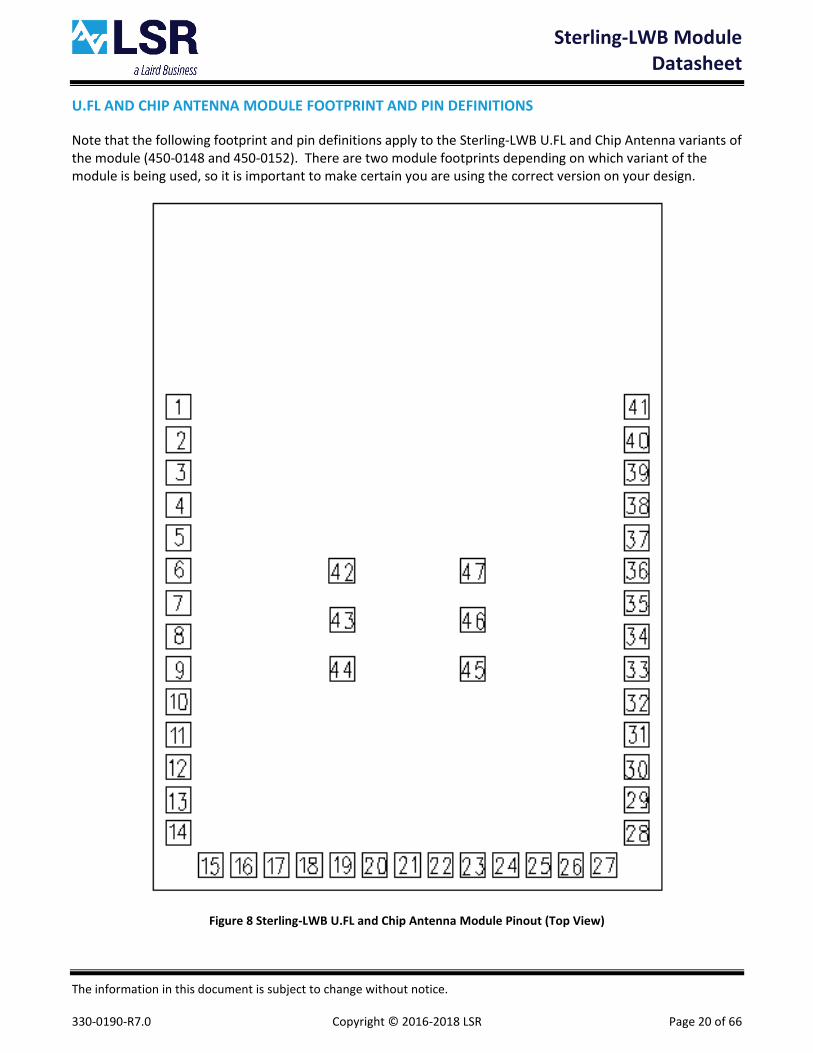
U.FL AND CHIP ANTENNA MODULE FOOTPRINT AND PIN DEFINITIONS
Note that the following footprint and pin definitions apply to the Sterling-LWB U.FL and Chip Antenna variants of the module (450-0148 and 450-0152). There are two module footprints depending on which variant of the module is being used, so it is important to make certain you are using the correct version on your design.
Figure 8 Sterling-LWB U.FL and Chip Antenna Module Pinout (Top View)

Sterling-LWB Module
Datasheet
The information in this document is subject to change without notice. 330-0190-R7.0 Copyright © 2016-2018 LSR Page 21 of 66
U.FL AND CHIP ANTENNA MODULE PIN DESCRIPTIONS
Module Pin
Name I/O Type Description
1 GND GND GROUND
2 BT_PCM_SYNC DIO PCM SYNC; CAN BE MASTER (OUTPUT) OR SLAVE (INPUT)
3 BT_PCM_IN DI PCM DATA INPUT SENSING
4 BT_PCM_OUT DO PCM DATA OUTPUT
5 VDD_3V3 PI WIFI AND BLUETOOTH POWER SUPPLY
6 GND GND GROUND
7 WIFI_GPIO_4 DIO PROGRAMMABLE GPIO PIN
8 WIFI_GPIO_3 DIO PROGRAMMABLE GPIO PIN
9 WIFI_GPIO_2 DIO PROGRAMMABLE GPIO PIN
10 WIFI_GPIO_1 DIO PROGRAMMABLE GPIO PIN
11 WIFI_GPIO_0 DIO PROGRAMMABLE GPIO PIN. THIS PIN BECOMES AN OUTPUT WHEN IT IS USED AS WLAN_HOST_WAKE/ OUT-OF-BAND SIGNAL.
12 WLREG_ON DI USED BY PMU TO POWER UP OR POWER DOWN THE INTERNAL REGULATORS USED BY THE WLAN SECTION.
13 CLK_REQ DO EXTERNAL SYSTEM CLOCK REQUEST – USED WHEN THE SYSTEM CLOCK IS NOT PROVIDED BY A DEDICATED CRYSTAL
14 GND GND GROUND
15 BT_GPIO_3 DIO PROGRAMMABLE GPIO PIN
16 BT_GPIO_4 DIO PROGRAMMABLE GPIO PIN
17 BT_GPIO_5 DIO PROGRAMMABLE GPIO PIN
18 GND GND GROUND
19 32KHZ_OSC_IN DI EXTERNAL SLEEP CLOCK INPUT
20 VDD_VIO PI DC SUPPLY FOR I/O
21 BT_REG_ON DI USED BY PMU TO POWER UP OR POWER DOWN THE INTERNAL REGULATORS USED BY THE BLUETOOTH SECTION.
22 SDIO_D0 DIO SDIO DATA LINE 0
23 SDIO_D1 DIO SDIO DATA LINE 1
24 GND GND GROUND
25 SDIO_D2 DIO SDIO DATA LINE 2
26 SDIO_CMD DIO SDIO COMMAND LINE
27 SDIO_D3 DIO SDIO DATA LINE 3

Sterling-LWB Module
Datasheet
The information in this document is subject to change without notice. 330-0190-R7.0 Copyright © 2016-2018 LSR Page 22 of 66
Module Pin
Name I/O Type Description
28 GND GND GROUND
29 SDIO_CK DIO SDIO CLOCK LINE
30 GND GND GROUND
31 BT_UART_RTS_L DO BT UART REQUEST-TO-SEND
32 BT_UART_CTS_L DI BT UART CLEAR-TO-SEND
33 BT_UART_TXD DO BT UART TRANSMIT OUTPUT
34 BT_UART_RXD DI BT UART RECEIVE INPUT
35 BT_I2S_CLK DIO I2S CLOCK; CAN BE MASTER (OUTPUT) OR SLAVE (INPUT)
36 BT_I2S_D0 DO I2S DATA OUTPUT
37 BT_I2S_WS DIO I2S_WS; CAN BE MASTER (OUTPUT) OR SLAVE (INPUT)
38 BT_PCM_CLK DIO PCM CLOCK; CAN BE MASTER (OUTPUT) OR SLAVE (INPUT)
39 BT_DEV_WAKE DIO DEV_WAKE OR GENERAL-PURPOSE I/O SIGNAL
40 BT_HOST_WAKE DO HOST_WAKE OR GENERAL-PURPOSE I/O SIGNAL
41 GND GND GROUND
42 GND GND GROUND
43 GND GND GROUND
44 GND GND GROUND
45 GND GND GROUND
46 GND GND GROUND
47 GND GND GROUND
PI = Power Input, DI = Digital Input, DO = Digital Output, DIO = Bi-directional Digital Port, GND = Ground
Table 4 Sterling-LWB U.FL and Chip Antenna Module Pin Descriptions

Sterling-LWB Module
Datasheet
The information in this document is subject to change without notice. 330-0190-R7.0 Copyright © 2016-2018 LSR Page 23 of 66
MODULE POWER STATES
The Sterling-LWB WLAN power states are described as follows: • Active mode- All WLAN blocks in the Sterling-LWB are powered up and fully functional with active carrier sensing and frame transmission and receiving. All required regulators are enabled and put in the most efficient mode based on the load current. Clock speeds are dynamically adjusted by the PMU sequencer. • Doze mode- The radio, analog domains, and most of the linear regulators are powered down. The rest of the BCM4343W remains powered up in an IDLE state. All main clocks (PLL, crystal oscillator) are shut down to reduce active power to the minimum. The 32.768 kHz LPO clock is available only for the PMU sequencer. This condition is necessary to allow the PMU sequencer to wake up the chip and transition to Active mode. In Doze mode, the primary power consumed is due to leakage current. • Deep-sleep mode- Most of the chip, including analog and digital domains, and most of the regulators are powered off. Logic states in the digital core are saved and preserved to retention memory in the always-on domain before the digital core is powered off. To avoid lengthy hardware re-initialization, the logic states in the digital core are restored to their pre-deep-sleep settings when a wake-up event is triggered by an external interrupt, a host resume through the SDIO bus, or by the PMU timers. • Power-down mode—The BCM4343W is effectively powered off by shutting down all internal regulators. The chip is brought out of this mode by external logic re-enabling the internal regulators.

Sterling-LWB Module
Datasheet
The information in this document is subject to change without notice.
330-0190-R7.0 Copyright © 2016-2018 LSR Page 24 of 66
U.FL AND CHIP ANTENNA MODULE PIN I/O STATES
Pin # Name
Keeper
(b)
Active Mode Low Power State/Sleep (All
Power Present)
Power Down(c) WL_REG_ON =0 BT_REG_ON = 0
Out of Reset: (VDD_VIO is present)
WL_REG_ON =1 BT_REG_ON = any
WL_REG_ON =1 BT_REG_ON = 0
WL_REG_ON =0 BT_REG_ON = 1
2 BT_PCM_SYNC Y Input No Pull(d) Input No Pull(d) High –Z No Pull(d) - Input,PD Input,PD
3 BT_PCM_IN Y Input No Pull(d) Input No Pull(d) High –Z No Pull(d) - Input,PD Input,PD
4 BT_PCM_OUT Y Input No Pull(d) Input No Pull(d) High –Z No Pull(d) - Input,PD Input,PD
7 WIFI_GPIO_4 Y TBD Active Mode High –Z No Pull(f) Input,GCI GPIO[1]
PU Active Mode Input,PU
8 WIFI_GPIO_3 Y TBD Active Mode High –Z No Pull(f) Input,GCI GPIO[0]
PU Active Mode Input,PU
9 WIFI_GPIO_2 Y TBD Active Mode High –Z No Pull(f) Input,GCI GPIO[7]
NoPull Active Mode Input,NoPull
10 WIFI_GPIO_1 Y TBD Active Mode High –Z No Pull(f) Input,PD Active Mode Input,PD
11 WIFI_GPIO_0 Y TBD Active Mode High –Z No Pull(f) Input,SDIO OOB Int.
NoPull Active Mode Input,NoPull
12 WLREG_ON N Input; PD (pull-down can be disabled)
Input; PD (pull-down can be disabled)
Input; PD (of 200K) Input; PD (of 200K) Input; PD (of 200K) -
13 CLK_REQ Y Open drain or push-pull(Active high)
Open drain or push-pull (Active high)
PD Open drain, (Active high)
Open drain, (Active high)
Open drain, (Active high)
21 BT_REG_ON N Input; PD (pull-down can be disabled)
Input; PD (pull-down can be disabled)
Input; PD (of 200K) Input; PD (of 200K) Input; PD (of 200K) Input; PD (of 200K)
22 SDIO_D0 N SDIO MODE -> NoPull
SDIO MODE -> NoPull
SDIO MODE -> NoPull
SDIO MODE ->PullUP SDIO MODE -> NoPull
Input,PU
23 SDIO_D1 N SDIO MODE -> NoPull
SDIO MODE -> NoPull
SDIO MODE -> NoPull
SDIO MODE ->PullUP SDIO MODE -> NoPull
Input,PU
25 SDIO_D2 N SDIO MODE -> NoPull
SDIO MODE -> NoPull
SDIO MODE -> NoPull
SDIO MODE ->PullUP SDIO MODE -> NoPull
Input,PU

Sterling-LWB Module
Datasheet
The information in this document is subject to change without notice.
330-0190-R7.0 Copyright © 2016-2018 LSR Page 25 of 66
Pin # Name
Keeper
(b)
Active Mode Low Power State/Sleep (All
Power Present)
Power Down(c) WL_REG_ON =0 BT_REG_ON = 0
Out of Reset: (VDD_VIO is present)
WL_REG_ON =1 BT_REG_ON = any
WL_REG_ON =1 BT_REG_ON = 0
WL_REG_ON =0 BT_REG_ON = 1
26 SDIO_CMD N SDIO MODE -> NoPull
SDIO MODE -> NoPull
SDIO MODE -> NoPull
SDIO MODE ->PullUP SDIO MODE -> NoPull
Input,PU
27 SDIO_D3 N SDIO MODE -> NoPull
SDIO MODE -> NoPull
SDIO MODE -> NoPull
SDIO MODE ->PullUP SDIO MODE -> NoPull
Input,PU
29 SDIO_CK N SDIO MODE -> NoPull
SDIO MODE -> NoPull
SDIO MODE -> NoPull
SDIO MODE ->NoPull SDIO MODE -> NoPull
Input
31 BT_UART_RTS_
L Y Output:NoPull Output:NoPull High-Z,NoPull - Input:PU Output:NoPull
32 BT_UART_CTS_
L Y Input:NoPull Input:NoPull High-Z,NoPull - Input:PU Input:NoPull
33 BT_UART_TXD Y Output:NoPull Output:NoPull High-Z,NoPull - Input:PU Output:NoPull
34 BT_UART_RXD Y Input:PU Input:NoPull High-Z,NoPull - Input:PU Input:NoPull
35 BT_I2S_CLK Y Input:NoPull(e) Input:NoPull(e) High-Z,NoPull - Input,PD Output: DrivenLow
36 BT_I2S_D0 Y Input:NoPull(e) Input:NoPull(e) High-Z,NoPull - Input,PD Input,PD
37 BT_I2S_WS Y Input:NoPull(e) Input:NoPull(e) High-Z,NoPull - Input,PD Input,PD
38 BT_PCM_CLK Y Input No Pull(d) Input No Pull(d) High –Z NoPull - Input,PD Input,PD
39 BT_DEV_WAKE Y I/O: PU,PD,NoPull
(Programmable) I/O: PU,PD,NoPull (Programmable)
High-Z,NoPull - Input,PD Output: DrivenLow
40 BT_HOST_WAK
E Y I/O: PU,PD,NoPull
(Programmable) I/O: PU,PD,NoPull (Programmable)
High-Z,NoPull - Input,PD Input,PD
Table 5 I/O States

Sterling-LWB Module
Datasheet
The information in this document is subject to change without notice.
330-0190-R7.0 Copyright © 2016-2018 LSR Page 26 of 66
The following notations are used: Input signal
• O: Output signal
• I/O: Input/Output signal • PU = Pulled up • PD = Pulled down • NoPull = Neither pulled up nor pulled down Notes: a. PU = pulled up, PD = pulled down. b. N = pad has no keeper. Y = pad has a keeper. Keeper is always active except in the power-down state. If there is no keeper, and it is an input and there is NoPull, then the pad should be driven to prevent leakage due to floating pad, for example, SDIO_CLK. c. In the Power-down state (xx_REG_ON = 0): High-Z; NoPull => The pad is disabled because power is not supplied. d. Depending on whether the PCM interface is enabled and the configuration is master or slave mode, it can be either an output or input. e. Depending on wether the I2S interface is enabled.and configuration is master or slave mode, itcan be either an input or output. f. The GPIO pull states for the active and low-power states are hardware defaults. They can all be subsequently programmed as a pull-up or pull-down.

Sterling-LWB Module
Datasheet
The information in this document is subject to change without notice. 330-0190-R7.0 Copyright © 2016-2018 LSR Page 27 of 66
GENERAL CHARACTERISTICS
General
Characteristic Description
Model Name Sterling-LWB
Product Description WiFi and Bluetooth Wireless Module
Dimension (SiP Module) 10 mm x 10 mm x 1.2 mm (W*L*T)
Dimension (Antenna Option Module) 15.5 mm x 21 mm x 2 mm (W*L*T)
Operating temperature -40°C to 85°C
Storage temperature -40°C to 125°C
Weight 0.9 g +/- 0.1g
Table 6 General Characteristics
DC Characteristics – General Purpose I/O
Parameter Test Conditions Min Typical Max Unit
Logic input low, VIL VDD_VIO = 1.8V - - 0.35x VDD_VIO V
Logic input high, VIH VDD_VIO = 1.8V 0.65x VDD_VIO - - V
Logic output low, VOL VDD_VIO = 1.8V 2mA - - 0.45 V
Logic output high, VOH VDD_VIO = 1.8V 2mA VDD_VIO-0.45 - - V
Logic input low, VIL VDD_VIO = 3.3V -- - 0.80 V
Logic input high, VIH VDD_VIO = 3.3V 2.00 - - V
Logic output low, VOL VDD_VIO = 3.3 2mA - - 0.40 V
Logic output high, VOH VDD_VIO = 3.3 2mA VDD_VIO-0.40 - - V
Table 7 DC Characteristics General Purpose I/O

Sterling-LWB Module
Datasheet
The information in this document is subject to change without notice. 330-0190-R7.0 Copyright © 2016-2018 LSR Page 28 of 66
DC Characteristics – SDO Interface Pins
Parameter Test Conditions Min Typical Max Unit
Logic input low, VIL VDD_VIO = 1.8V - - 0.58 V
Logic input high, VIH VDD_VIO = 1.8V 1.27 - - V
Logic output low, VOL VDD_VIO = 1.8V 2mA - - 0.45 V
Logic output high, VOH VDD_VIO = 1.8V 2mA 1.4 - - V
Logic input low, VIL VDD_VIO = 3.3V 0.625x VDD_VIO - - V
Logic input high, VIH VDD_VIO = 3.3V - - 0.25x VDD_VIO V
Logic output low, VOL VDD_VIO = 3.3 @ 2mA - - 0.125x VDD_VIO V
Logic output high, VOH VDD_VIO = 3.3 @ 2mA 0.75x VDD_VIO - - V
Figure 9 DC Characteristics SDIO I/O
RF Characteristics
Parameter Min Typical Max Unit
RF frequency range 2400 2500 MHz
RF data rate 1 802.11 b/g/n rates supported 65 Mbps
Table 8 RF Characteristics
Sterling-LWB Module
Datasheet
The information in this document is subject to change without notice. 330-0190-R7.0 Copyright © 2016-2018 LSR Page 29 of 66
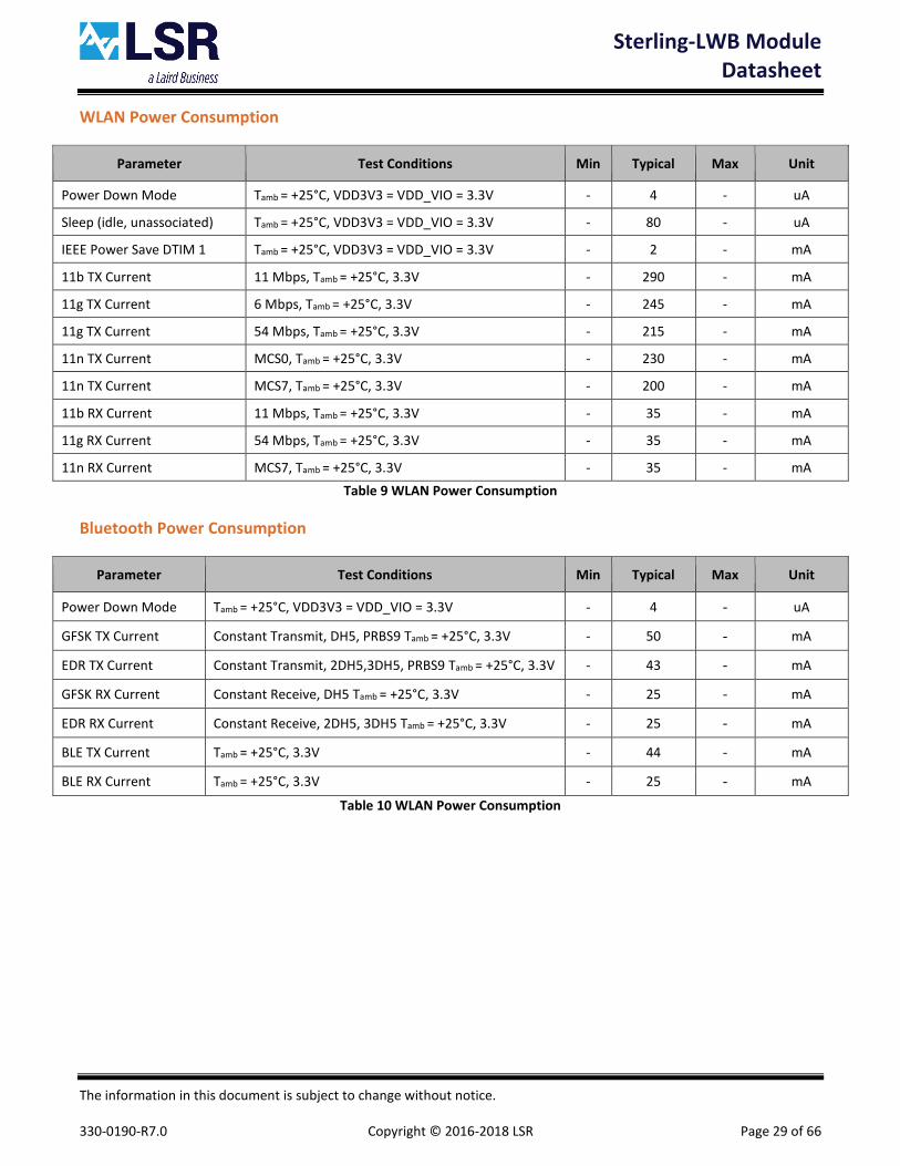
WLAN Power Consumption
Parameter Test Conditions Min Typical Max Unit
Power Down Mode Tamb = +25°C, VDD3V3 = VDD_VIO = 3.3V - 4 - uA
Sleep (idle, unassociated) Tamb = +25°C, VDD3V3 = VDD_VIO = 3.3V - 80 - uA
IEEE Power Save DTIM 1 Tamb = +25°C, VDD3V3 = VDD_VIO = 3.3V - 2 - mA
11b TX Current 11 Mbps, Tamb = +25°C, 3.3V - 290 - mA
11g TX Current 6 Mbps, Tamb = +25°C, 3.3V - 245 - mA
11g TX Current 54 Mbps, Tamb = +25°C, 3.3V - 215 - mA
11n TX Current MCS0, Tamb = +25°C, 3.3V - 230 - mA
11n TX Current MCS7, Tamb = +25°C, 3.3V - 200 - mA
11b RX Current 11 Mbps, Tamb = +25°C, 3.3V - 35 - mA
11g RX Current 54 Mbps, Tamb = +25°C, 3.3V - 35 - mA
11n RX Current MCS7, Tamb = +25°C, 3.3V - 35 - mA
Table 9 WLAN Power Consumption
Bluetooth Power Consumption
Parameter Test Conditions Min Typical Max Unit
Power Down Mode Tamb = +25°C, VDD3V3 = VDD_VIO = 3.3V - 4 - uA
GFSK TX Current Constant Transmit, DH5, PRBS9 Tamb = +25°C, 3.3V - 50 - mA
EDR TX Current Constant Transmit, 2DH5,3DH5, PRBS9 Tamb = +25°C, 3.3V - 43 - mA
GFSK RX Current Constant Receive, DH5 Tamb = +25°C, 3.3V - 25 - mA
EDR RX Current Constant Receive, 2DH5, 3DH5 Tamb = +25°C, 3.3V - 25 - mA
BLE TX Current Tamb = +25°C, 3.3V - 44 - mA
BLE RX Current Tamb = +25°C, 3.3V - 25 - mA
Table 10 WLAN Power Consumption

Sterling-LWB Module
Datasheet
The information in this document is subject to change without notice. 330-0190-R7.0 Copyright © 2016-2018 LSR Page 30 of 66
Power Supply Requirements
Power Supply Requirements Min Typical Max Unit
VDD_VIO 1.8 3.3 3.6 V
VDD_VIO Current - 300 - uA
VDD_3V3 3.0 3.3 3.6 V
VDD_3V3 Current - See Note* - mA
Table 11 Power Supply Requirements
* Note: See WLAN and Bluetooth Power Consumption Table for various steady-state operating values. This value is the typical peak current required for the Radio Transmitter Calibration Mode. See Current Waveform in Calibration Current Profile shown below.

Sterling-LWB Module
Datasheet
The information in this document is subject to change without notice. 330-0190-R7.0 Copyright © 2016-2018 LSR Page 31 of 66
Calibration Current Profile
Although the Max continuous supply current to the module is <300 mA, when providing power to the module, a power source capable of supplying 600 mA peak current for a duration of ~20 mSec is required by the module transmitter during calibration.
Module calibration occurs:
(1) When the Module is initially powered up. (2) The module is reset. (3) When the radio is initialized. (4) Every 2 minutes after the radio is initialized.
Note: Radio calibration will not occur while the module is in modes Doze, Deep Sleep, Power Down or if the radio is not initialized.
Figure 10 shows the current profile of the Sterling-LWB module during calibration. If current is limited to <600mA during this process, the module will fail to calibrate.
Figure 10 Module RF Calibration Current Profile

Sterling-LWB Module
Datasheet
The information in this document is subject to change without notice. 330-0190-R7.0 Copyright © 2016-2018 LSR Page 32 of 66
CRYSTAL OSCILLATOR REQUIREMENTS
32.768 KHz Oscillator
Frequency Accuracy ± 200 ppm
Duty Cycle 30% - 70%
Input Signal Amplitude 200 – 3300 mV, p-p
Signal Type Square or Sine Wave
Clock Jitter <10,000 ppm
Table 12 Oscillator Requirements
Note: A 32.768 KHz crystal is required in order for the module to be fully functional. The module will not boot without it.

Sterling-LWB Module
Datasheet
The information in this document is subject to change without notice. 330-0190-R7.0 Copyright © 2016-2018 LSR Page 33 of 66
CONTROL SIGNAL TIMING DIAGRAMS
Figure 11 WLAN = ON, Bluetooth = ON
Figure 12 WLAN = OFF, Bluetooth = OFF

Sterling-LWB Module
Datasheet
The information in this document is subject to change without notice. 330-0190-R7.0 Copyright © 2016-2018 LSR Page 34 of 66
Figure 13 WLAN = ON, Bluetooth = OFF
Figure 14 WLAN = OFF, Bluetooth = ON
Note: For both the WL_REG_ON and BT_REG_ON pins, there should be at least a 10 ms time delay between consecutive toggles (where both signals have been driven low). This is to allow time for the CBUCK regulator to discharge. If this delay is not followed, then there may be a VDDIO in-rush current on the order of 36 mA during the next PMU cold start.

Sterling-LWB Module
Datasheet
The information in this document is subject to change without notice. 330-0190-R7.0 Copyright © 2016-2018 LSR Page 35 of 66
WLAN RF Characteristics WLAN Transmitter Characteristics (TA = +25°C, VCC = 3.3 V)
Parameter Test Conditions Min Typ Max Unit
1 Mbps DSSS (b) TX Output Power 1 Mbps BPSK 802.11(b) Mask Compliance 35% EVM RMS power over TX packet
- 17.5 - dBm
2 Mbps DSSS (b) TX Output Power 2 Mbps QPSK 802.11(b) Mask Compliance 35% EVM RMS power over TX packet
- 17.5 - dBm
5.5 Mbps DSSS (b) TX Output Power 5.5 Mbps QPSK 802.11(b) Mask Compliance 35% EVM RMS power over TX packet
- 17.5 - dBm
11 Mbps DSSS (b) TX Output Power 11 Mbps CCK 802.11(b) Mask Compliance 35% EVM RMS power over TX packet
- 17.5 - dBm
6 Mbps OFDM (g) TX Output Power 6 Mbps BPSK 802.11(g) Mask Compliance -5 dB EVM RMS power over TX packet
- 14.0 - dBm
9 Mbps OFDM (g) TX Output Power 9 Mbps BPSK 802.11(g) Mask Compliance -8 dB EVM RMS power over TX packet
- 14.0 - dBm
12 Mbps OFDM (g) TX Output Power 12 Mbps QPSK 802.11(g) Mask Compliance -10 dB EVM RMS power over TX packet
- 14.0 - dBm
18 Mbps OFDM (g) TX Output Power 18 Mbps QPSK 802.11(g) Mask Compliance -13 dB EVM RMS power over TX packet
- 14.0 - dBm
24 Mbps OFDM (g) TX Output Power 24 Mbps 16-QAM 802.11(g) Mask Compliance -16 dB EVM RMS power over TX packet
- 14.0 - dBm
36 Mbps OFDM (g) TX Output Power 36 Mbps 16-QAM 802.11(g) Mask Compliance -19 dB EVM RMS power over TX packet
- 14.0 - dBm
48 Mbps OFDM (g) TX Output Power 48 Mbps 64-QAM 802.11(g) Mask Compliance -22 dB EVM RMS power over TX packet
- 14.0 - dBm
54 Mbps OFDM (g) TX Output Power 54 Mbps 64-QAM 802.11(g) Mask Compliance -25 dB EVM RMS power over TX packet
- 14.0 - dBm
MCS0 OFDM (n) TX Output Power 6.5 Mbps BPSK 802.11(n) Mask Compliance -5 dB EVM RMS power over TX packet
- 12.5 - dBm
MCS1 OFDM (n) TX Output Power 13 Mbps QPSK 802.11(n) Mask Compliance -10 dB EVM RMS power over TX packet
- 12.5 - dBm
MCS2 OFDM (n) TX Output Power 19.5 Mbps QPSK 802.11(n) Mask Compliance -13 dB EVM RMS power over TX packet
- 12.5 - dBm
MCS3 OFDM (n) TX Output Power 26 Mbps 16-QAM 802.11(n) Mask Compliance -16 dB EVM RMS power over TX packet
- 12.5 - dBm
MCS4 OFDM (n) TX Output Power 39 Mbps 16-QAM 802.11(n) Mask Compliance -19 dB EVM RMS power over TX packet
- 12.5 - dBm
MCS5 OFDM (n) TX Output Power 52 Mbps 64-QAM 802.11(n) Mask Compliance -22 dB EVM RMS power over TX packet
- 12.5 - dBm
MCS6 OFDM (n) TX Output Power 58.5 Mbps 64-QAM 802.11(n) Mask Compliance -25 dB EVM RMS power over TX packet
- 12.5 - dBm
MCS7 OFDM (n) TX Output Power 65 Mbps 64-QAM 802.11(n) Mask Compliance -27 dB EVM RMS power over TX packet
- 12.5 - dBm
Table 13 WLAN Transmitter RF Characteristics

Sterling-LWB Module
Datasheet
The information in this document is subject to change without notice. 330-0190-R7.0 Copyright © 2016-2018 LSR Page 36 of 66
WLAN Receiver Characteristics (TA = +25°C, VCC = 3.3 V)
Parameter Test Conditions Min Typ Max Unit
1 Mbps DSSS (b) RX Sensitivity 8% PER - -94 - dBm
2 Mbps DSSS (b) RX Sensitivity 8% PER - -93 - dBm
5.5 Mbps DSSS (b) RX Sensitivity 8% PER - -91 - dBm
11 Mbps DSSS (b) RX Sensitivity 8% PER - -88 - dBm
6 Mbps OFDM (g) RX Sensitivity 10% PER - -90 - dBm
9 Mbps OFDM (g) RX Sensitivity 10% PER - -89 - dBm
12 Mbps OFDM (g) RX Sensitivity 10% PER - -87 - dBm
18 Mbps OFDM (g) RX Sensitivity 10% PER - -85 - dBm
24 Mbps OFDM (g) RX Sensitivity 10% PER - -83 - dBm
36 Mbps OFDM (g) RX Sensitivity 10% PER - -80 - dBm
48 Mbps OFDM (g) RX Sensitivity 10% PER - -76 - dBm
54 Mbps OFDM (g) RX Sensitivity 10% PER - -75 - dBm
MCS0 (6.5 Mbps) OFDM (n) RX Sensitivity 10% PER - -89 - dBm
MCS1 (13 Mbps) OFDM (n) RX Sensitivity 10% PER - -86 - dBm
MCS2 (19.5 Mbps) OFDM (n) RX Sensitivity 10% PER - -84 - dBm
MCS3 26 Mbps OFDM (n) RX Sensitivity 10% PER - -82 - dBm
MCS4 39 Mbps OFDM (n) RX Sensitivity 10% PER - -79 - dBm
MCS5 52 Mbps OFDM (n) RX Sensitivity 10% PER - -75 - dBm
MCS6 58.5 Mbps OFDM (n) RX Sensitivity 10% PER - -73 - dBm
MCS7 65 Mbps OFDM (n) RX Sensitivity 10% PER - -72 - dBm
11b RX Overload Level 8% PER, 11 Mbps -10 - - dBm
11g RX Overload Level 10% PER, 54 Mbps -20 - - dBm
11n RX Overload Level 10% PER, MCS7 -20 - - dBm
Table 14 WLAN Receiver RF Characteristics

Sterling-LWB Module
Datasheet
The information in this document is subject to change without notice. 330-0190-R7.0 Copyright © 2016-2018 LSR Page 37 of 66
Bluetooth RF Characteristics
Bluetooth Transmitter GFSK & EDR Characteristics (TA=25°C, VBAT=3.3 V)
Parameter Test Conditions Min Typical Max Bluetooth Spec Unit
GFSK RF Output Power - 8.5 - dBm
EDR RF Output Power - 4.0 - dBm
Power Control Step Size 2 4 8 2-8 dB
EDR Relative Power -4 1 -4/+1 dB
Table 15 Bluetooth
Bluetooth Receiver GFSK & EDR Characteristics (TA=25°C, VBAT=3.3 V)
Parameter Test Conditions Min Typical Max Bluetooth Spec Unit
GFSK Sensitivity BER=0.1% - -90 - -70 dBm
EDR 2 Mbps Sensitivity BER=0.01% - -92 - -70 dBm
EDR 3 Mbps Sensitivity BER=0.01% - -87 - -70 dBm
GFSK Maximum Input Level BER=0.1% - -20 - -20 dBm
EDR 2 Maximum Input Level BER=0.01% - -20 - - dBm
EDR 3 Maximum Input Level BER=0.01% - -20 - - dBm
Table 16 Bluetooth
BLE Transmitter Characteristics (TA=25°C, VBAT=3.3 V)
Parameter Test Conditions Min Typical Max Bluetooth Spec Unit
GFSK RF Output Power - 7.5 - dBm
Power Control Step Size 2 4 8 2-8 dB
Table 17 Bluetooth
BLE Receiver Characteristics (TA=25°C, VBAT=3.3 V)
Parameter Test Conditions Min Typical Max Bluetooth Spec Unit
GFSK Sensitivity PER = 30.8% - -94 - -70 dBm
GMSK Maximum Input Level PER = 30.8% - -20 - -20 dBm
Table 18 Bluetooth
Sterling-LWB Module
Datasheet
The information in this document is subject to change without notice. 330-0190-R7.0 Copyright © 2016-2018 LSR Page 38 of 66
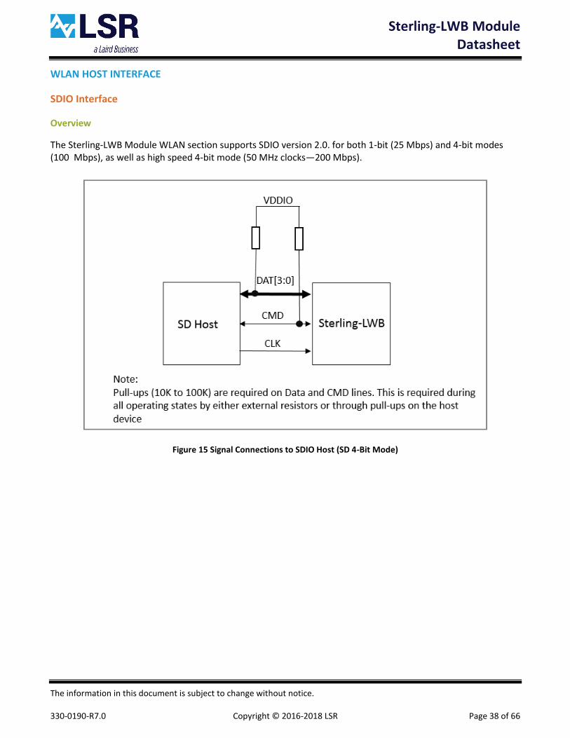
WLAN HOST INTERFACE
SDIO Interface
Overview
The Sterling-LWB Module WLAN section supports SDIO version 2.0. for both 1-bit (25 Mbps) and 4-bit modes (100 Mbps), as well as high speed 4-bit mode (50 MHz clocks—200 Mbps).
Figure 15 Signal Connections to SDIO Host (SD 4-Bit Mode)

Sterling-LWB Module
Datasheet
The information in this document is subject to change without notice. 330-0190-R7.0 Copyright © 2016-2018 LSR Page 39 of 66
Figure 16 Signal Connections to SDIO Host (SD 1-Bit Mode)

Sterling-LWB Module
Datasheet
The information in this document is subject to change without notice. 330-0190-R7.0 Copyright © 2016-2018 LSR Page 40 of 66
BLUETOOTH UART HOST INTERFACE
Overview
The Sterling-LWB uses a single UART for Bluetooth. The UART is a standard 4-wire interface (RX, TX, RTS, and CTS) with adjustable baud rates from 9600 bps to 4.0 Mbps. The interface features an automatic baud rate detection capability that returns a baud rate selection. The baud rate may be selected through a vendor-specific UART HCI command to a value other than the default rate of 115.2 kbps.
Figure 17 UART Connection from Sterling-LWB to Host

Sterling-LWB Module
Datasheet
The information in this document is subject to change without notice. 330-0190-R7.0 Copyright © 2016-2018 LSR Page 41 of 66
Soldering Recommendations
Reflow for Lead Free Solder Paste
• Optimal solder reflow profile depends on solder paste properties and should be optimized as part of an overall process development.
• It is important to provide a solder reflow profile that matches the solder paste supplier's recommendations.
• Temperature ranges beyond that of the solder paste supplier's recommendation could result in poor solderability.
• All solder paste suppliers recommend an ideal reflow profile to give the best solderability.
Recommended Reflow Profile for Lead Free Solder
Figure 18 Recommended Soldering Profile
Note: The quality of solder joints on the surface mount pads where they contact the host board should meet the appropriate IPC Specification. See IPC-A-610-D Acceptability of Electronic Assemblies, section 8.2.1 “Bottom Only Terminations.”

Sterling-LWB Module
Datasheet
The information in this document is subject to change without notice. 330-0190-R7.0 Copyright © 2016-2018 LSR Page 42 of 66
WIFI MAC IDS/BLUETOOTH MAC IDS
LSR has procured a block of IEEE MAC Address from the IEEE association. The MAC addresses are six (6) bytes in length and the three (3) Most Significant Bytes (MSBs) are the OUI, which is used to identify the company to which the block of IEEE addresses was assigned. LSR’s OUI is 00:25:CA.
For the Sterling-LWB, the WiFi MAC ID and Bluetooth MAC ID is preprogrammed during production for each module. The Bluetooth MAC ID is the WiFi MAC ID plus one.
Example:
WiFi MAC ID Bluetooth MAC ID
Module 1 00:25:CA:07:00:01 00:25:CA:07:00:02
Module 2 00:25:CA:07:00:03 00:25:CA:07:00:04
Module 3 00:25:CA:07:00:05 00:25:CA:07:00:06
Module 4 00:25:CA:07:00:07 00:25:CA:07:00:08
Table 19 Example MAC ID Assignments

Sterling-LWB Module
Datasheet
The information in this document is subject to change without notice. 330-0190-R7.0 Copyright © 2016-2018 LSR Page 43 of 66
CLEANING
In general, cleaning the populated modules is strongly discouraged. Residuals under the module cannot be easily removed with any cleaning process.
• Cleaning with water can lead to capillary effects where water is absorbed into the gap between the host board and the module. The combination of soldering flux residuals and encapsulated water could lead to short circuits between neighboring pads. Water could also damage any stickers or labels.
• Cleaning with alcohol or a similar organic solvent will likely flood soldering flux residuals into the RF shield, which is not accessible for post-washing inspection. The solvent could also damage any stickers or labels.
• Ultrasonic cleaning could damage the module permanently.
OPTICAL INSPECTION
After soldering the Module to the host board, consider optical inspection to check the following:
• Proper alignment and centering of the module over the pads.
• Proper solder joints on all pads.
• Excessive solder or contacts to neighboring pads, or vias.
REWORK
The Sterling-LWB module can be unsoldered from the host board if the Moisture Sensitivity Level (MSL) requirements are met as described in this datasheet.
Never attempt a rework on the module itself, e.g. replacing individual components. Such actions will terminate warranty coverage.
SHIPPING, HANDLING, AND STORAGE
Shipping
Bulk orders of the Sterling-LWB base module are delivered in reels of 2000. Bulk orders for the antenna option PCBAs are delivered in reels of 1000.
Handling
The Sterling-LWB modules contain a highly sensitive electronic circuitry. Handling without proper ESD protection may damage the module permanently.
Moisture Sensitivity Level (MSL)
Per J-STD-020, devices rated as MSL 4 and not stored in a sealed bag with desiccant pack should be baked prior to use.
Devices are packaged in a Moisture Barrier Bag with a desiccant pack and Humidity Indicator Card (HIC). Devices that will be subjected to reflow should reference the HIC and J-STD-033 to determine if baking is required.
If baking is required, refer to J-STD-033 for bake procedure.
Storage
Per J-STD-033, the shelf life of devices in a Moisture Barrier Bag is 12 months at <40C and <90% room humidity (RH).
Do not store in salty air or in an environment with a high concentration of corrosive gas, such as Cl2, H2S, NH3, SO2, or NOX.
Do not store in direct sunlight.
The product should not be subject to excessive mechanical shock.
Sterling-LWB Module
Datasheet
The information in this document is subject to change without notice. 330-0190-R7.0 Copyright © 2016-2018 LSR Page 44 of 66
Repeated Reflow Soldering
Only a single reflow soldering process is encouraged for host boards.

Sterling-LWB Module
Datasheet
The information in this document is subject to change without notice. 330-0190-R7.0 Copyright © 2016-2018 LSR Page 45 of 66
AGENCY CERTIFICATIONS
FCC ID: TFB-1003, 15.247
IC ID: 5969A-1003, RSS 247
CE: Compliant to standards EN 60950-1, EN 300 328, and EN 301 489 Giteki: 209-J00212 RCM: Compliant to standards EN 300 328 V1.9.1, AS/NZS 4268: 2012-A1:2013, and EN 55022:2010/AC:2011
AGENCY STATEMENTS
Federal Communication Commission Interference Statement
This equipment has been tested and found to comply with the limits for a Class B digital device, pursuant to Part 15 of the FCC Rules. These limits are designed to provide reasonable protection against harmful interference in a residential installation. This equipment generates uses and can radiate radio frequency energy and, if not installed and used in accordance with the instructions, may cause harmful interference to radio communications. However, there is no guarantee that interference will not occur in a particular installation. If this equipment does cause harmful interference to radio or television reception, which can be determined by turning the equipment off and on, the user is encouraged to try to correct the interference by one of the following measures:
• Reorient or relocate the receiving antenna.
• Increase the separation between the equipment and receiver.
• Connect the equipment into an outlet on a circuit different from that to which the receiver is connected.
• Consult the dealer or an experienced radio/TV technician for help.
This device complies with Part 15 of the FCC Rules. Operation is subject to the following two conditions: (1) This device may not cause harmful interference, and (2) this device must accept any interference received, including interference that may cause undesired operation.
FCC CAUTION: Any changes or modifications not expressly approved by the party responsible for compliance could void the user's authority to operate this equipment.

Sterling-LWB Module
Datasheet
The information in this document is subject to change without notice. 330-0190-R7.0 Copyright © 2016-2018 LSR Page 46 of 66
Industry Canada Statements
This Device complies with Industry Canada License-exempt RSS standard(s). Operation is subject to the following two conditions: (1) this device may not cause interference, and (2) this device must accept any interference, including interference that may cause undesired operation of the device.
To reduce potential radio interference to other users, the antenna type and its gain should be so chosen that the equivalent isotropically radiated power (e.i.r.p.) is not more than that permitted for successful communication.
This device has been designed to operate with the antenna(s) listed below, and having a maximum gain of 2.0 dBi (LSR Dipole), 2.0 dBi (LSR FlexPIFA), 2.0 dBi (LSR FlexNotch), 2.0 dBi (LSR mFlexPIFA), and 1.5 dBi (Johanson Chip). Antennas not included in this list or having a gain greater than 2.0 dBi, 2.0 dBi, 2.0 dBi, 2.0 dBi, and 1.5 dBi are strictly prohibited for use with this device. The required antenna impedance is 50 ohms.
List of all Antennas Acceptable for use with the Transmitter
1) LSR 001-0001 center-fed 2.4 GHz dipole antenna and LSR 080-0001 U.FL to Reverse Polarity SMA connector cable.
2) LSR 001-0014 2.4 GHz FlexPIFA antenna.
3) LSR 001-0015 2.4 GHz FlexNotch antenna.
4) LSR 001-0030 2.4 GHz Metal FlexPIFA (mFlexPIFA) antenna.
5) Johanson Technology 2450AT18D0100 chip antenna.
Cet appareil est conforme avec Industrie Canada, exempts de licence standard RSS (s). L'opération est soumise aux deux conditions suivantes: (1) cet appareil ne peut pas provoquer d'interférences et (2) cet appareil doit accepter toute interférence, y compris les interférences qui peuvent causer un mauvais fonctionnement de l'appareil.
Pour réduire le risque d'interférence aux autres utilisateurs, le type d'antenne et son gain doiventêtre choisis de manière que la puissance isotrope rayonnée équivalente (PIRE) ne dépasse pascelle permise pour une communication réussie.
Cet appareil a été conçu pour fonctionner avec l'antenne (s) ci-dessous, et ayant un gain maximum de 2,0 dBi (LSR Dipole), 2,0 dBi (LSR FlexPIFA), 2,0 dBi (LSR FlexNotch), 2,0 dBi (LSR mFlexPIFA), et 1,5 dBi (Johanson Chip). Antennes pas inclus dans cette liste ou présentant un gain supérieure à 2,0 dBi, 2,0 dBi, 2,0 dBi, 2,0 dBi, et 1,5 dBi sont strictement interdits pour une utilisation avec cet appareil. L'impédance d'antenne requise est de 50 ohms.
Liste de toutes les antennes acceptables pour une utilisation avec l'émetteur
1) Antenne LSR 001-0001 2.4 GHz de centre-dipôle alimenté et LSR 080-0001 U.FL inverser câble connecteur SMA à polarité.
2) LSR 001-0014 antenne FlexPIFA 2,4 GHz w/U.FL câble.
3) LSR 001-0015 antenne FlexNotch 2,4 GHz w/U.FL câble.
4) LSR 001-0030 antenne Métal FlexPIFA (mFlexPIFA) 2,4 GHz.
5) Antenne de puce Johanson Technology 2450AT18D0100.

Sterling-LWB Module
Datasheet
The information in this document is subject to change without notice. 330-0190-R7.0 Copyright © 2016-2018 LSR Page 47 of 66
OEM RESPONSIBILITIES TO COMPLY WITH FCC AND INDUSTRY CANADA REGULATIONS
The Sterling-LWB Module has been certified for integration into products only by OEM integrators under the following conditions:
To comply with FCC and Industry Canada RF exposure limits for general population / uncontrolled exposure, the antenna must be installed to provide a separation distance of at least 29mm from all persons and operating in conjunction with any other antenna or transmitter, except in accordance with FCC multi-transmitter product procedures.
As long as the two conditions above are met, further transmitter testing will not be required. However, the OEM integrator is still responsible for testing their end-product for any additional compliance requirements required with this module installed (for example, digital device emissions, PC peripheral requirements, etc.).
IMPORTANT NOTE: In the event that these conditions cannot be met (for certain configurations or co-location with another transmitter), then the FCC and Industry Canada authorizations are no longer considered valid and the FCC ID and IC Certification Number cannot be used on the final product. In these circumstances, the OEM integrator will be responsible for re-evaluating the end product (including the transmitter) and obtaining a separate FCC and Industry Canada authorization.
Le module de Sterling-LWB a été certifié pour l'intégration dans des produits uniquement par des intégrateurs OEM dans les conditions suivantes:
Pour se conformer aux limites d'exposition aux RF de la FCC et d'Industrie Canada pour la population générale / exposition non contrôlée, l'antenne doit être installé pour fournir une distance de séparation d'au moins 29mm de toutes les personnes et fonctionnant conjointement avec une autre antenne ou émetteur, sauf en conformité avec la FCC procédures de produits multi- émetteurs.
Tant que les deux conditions précitées sont réunies, les tests de transmetteurs supplémentaires ne seront pas tenus. Toutefois, l'intégrateur OEM est toujours responsable de tester leur produit final pour toutes les exigences de conformité supplémentaires requis avec ce module installé (par exemple, les émissions appareil numérique, les exigences de périphériques PC, etc.)
NOTE IMPORTANTE: Dans le cas où ces conditions ne peuvent être satisfaites (pour certaines configurations ou de co-implantation avec un autre émetteur), puis la FCC et Industrie autorisations Canada ne sont plus considérés comme valides et l'ID de la FCC et IC numéro de certification ne peut pas être utilisé sur la produit final. Dans ces circonstances, l'intégrateur OEM sera chargé de réévaluer le produit final (y compris l'émetteur) et l'obtention d'un distincte de la FCC et Industrie Canada l'autorisation.

Sterling-LWB Module
Datasheet
The information in this document is subject to change without notice. 330-0190-R7.0 Copyright © 2016-2018 LSR Page 48 of 66
OEM LABELING REQUIREMENTS FOR END-PRODUCT
The Sterling-LWB module is labeled with its own FCC ID and IC Certification Number. The FCC ID and IC certification numbers are not visible when the module is installed inside another device, as such the end device into which the module is installed must display a label referring to the enclosed module. The final end product must be labeled in a visible area with the following:
“Contains Transmitter Module FCC ID: TFB-1003”
“Contains Transmitter Module IC: 5969A-1003”
or
“Contains FCC ID: TFB-1003”
“Contains IC: 5969A-1003”
The OEM of the Sterling-LWB Module must only use the approved antenna(s) listed above, which have been certified with this module.
Le module de Sterling-LWB est étiqueté avec son propre ID de la FCC et IC numéro de certification. L'ID de la FCC et IC numéros de certification ne sont pas visibles lorsque le module est installé à l'intérieur d'un autre appareil, comme par exemple le terminal dans lequel le module est installé doit afficher une etiquette faisant référence au module ci-joint. Le produit final doit être étiqueté dans un endroit visible par le suivant: “Contient Module émetteur FCC ID: TFB-1003" “Contient Module émetteur IC: 5969A-1003" ou “Contient FCC ID: TFB-1003" “Contient IC: 5969A-1003" Les OEM du module Sterling-LWB ne doit utiliser l'antenne approuvée (s) ci-dessus, qui ont été certifiés avec ce module.
Sterling-LWB Module
Datasheet
The information in this document is subject to change without notice. 330-0190-R7.0 Copyright © 2016-2018 LSR Page 49 of 66
OEM END PRODUCT USER MANUAL STATEMENTS
The OEM integrator should not to provide information to the end user regarding how to install or remove this RF module or change RF related parameters in the user manual of the end product.
The user manual for the end product must include the following information in a prominent location:
To comply with FCC and Industry Canada RF exposure limits for general population / uncontrolled exposure, the antenna(s) used for this transmitter must be installed to provide a separation distance of at least 29mm from all persons and operating in conjunction with any other antenna or transmitter, except in accordance with FCC multi-transmitter product procedures.
Other user manual statements may apply.
L'intégrateur OEM ne devraient pas fournir des informations à l'utilisateur final sur la façon d'installer ou de supprimer ce module RF ou modifier les paramètres liés RF dans le manuel utilisateur du produit final. Le manuel d'utilisation pour le produit final doit comporter les informations suivantes dans unendroit bien en vue: Pour se conformer aux limites d'exposition aux RF de la FCC et d'Industrie Canada pour la population générale / exposition non contrôlée, l'antenne(s) utilisée pour ce transmetteur doit être installé pour fournir une distance de séparation d'au moins 29mm de toutes les personnes et fonctionnant conjointement avec une autre antenne ou émetteur, sauf en conformité avec les procédures de produits multi- émetteur FCC. Autres déclarations manuel de l'utilisateur peuvent s'appliquer.

Sterling-LWB Module
Datasheet
The information in this document is subject to change without notice. 330-0190-R7.0 Copyright © 2016-2018 LSR Page 50 of 66
EUROPE
CE Notice
This device has been tested and certified for use in the European Union. See the Declaration of Conformity (DOC) for specifics.
If this device is used in a product, the OEM has responsibility to verify compliance of the final product to the EU standards. A Declaration of Conformity must be issued and kept on file as described in the Radio and Telecommunications Terminal Equipment (R&TTE) Directive. The ‘CE’ mark must be placed on the OEM product per the labeling requirements of the Directive.
Declaration of Conformity (DOC)
This DOC can be downloaded from the LSR Website.
AUSTRALIA
RCM
Radiocommunications (Short Range Devices) Standard 2014 (Amnt 1:2015) Radiocommunications (Low Interference Potential Device) Class License 2015
AS/NZS 4268: 2012-A1:2013 EN 300328 V1.9.1 Report No.: 316052 (316051), Dated: 21 July 2016, LS Research
Radiocommunications (Electromagnetic Compatibility) Standard 2008
EN 55022 : 2010/AC :2011 Information Technology Equipment – Radio disturbance characteristics – Limits and methods measurement Report No. : TR 316051 B, dated : 6 July 2016, LS Research
Radiocommunications (Electromagnetic Radiation – Human Exposure) Standard 2014
Maximum Exposure Levels to Radio Frequency Fields – 3 KHz to 300 GHz (2002) RPS 3, ARPANSA Category B Exemption – Fixed Station Exemption, ARPANSA Schedule 5, General Public Exposure, <20mW Mean Power, Or no antenna near the body (>20cm from unaware user) and mean output power does not exceed Table 2 threshold for testing.
Table 20 AU/NZS Certification
If this device is used in a product, the OEM has responsibility to verify compliance of the final end product to the Australia/New Zealand (RCM) Standards. All end-products require their own certification (SDoc). You will not be able to leverage the module certification and ship product into the country.

Sterling-LWB Module
Datasheet
The information in this document is subject to change without notice. 330-0190-R7.0 Copyright © 2016-2018 LSR Page 51 of 66
BLUETOOTH SIG QUALIFICATION
Overview
The Sterling-LWB module is listed on the Bluetooth SIG website as a qualified Controller Subsystem.
Design Name Owner Declaration ID Link to listing on the SIG website
450-0159 Laird D031500 Sterling-LWB 450-0159
450-0148 Laird D031500 Sterling-LWB 450-0148
450-0152 Laird D031500 Sterling-LWB 450-0152
Table 21 Sterling-LWB Declaration ID
It is a mandatory requirement of the Bluetooth Special Interest Group (SIG) that every product implementing Bluetooth technology has a Declaration ID. Every Bluetooth design is required to go through the qualification process, even when referencing a Bluetooth Design that already has its own Declaration ID. The Qualification Process requires each company to register as a member of the Bluetooth SIG – www.bluetooth.org The following is a link to the Bluetooth Registration page: https://www.bluetooth.org/login/register/ For each Bluetooth Design it is necessary to purchase a Declaration ID. This can be done before starting the new qualification, either through invoicing or credit card payment. The fees for the Declaration ID will depend on your membership status, please refer to the following webpage: https://www.bluetooth.org/en-us/test-qualification/qualification-overview/fees For a detailed procedure of how to obtain a new Declaration ID for your design, please refer to the following SIG document, (login is required to views this document): https://www.bluetooth.org/DocMan/handlers/DownloadDoc.ashx?doc_id=283698&vId=317486
Qualification Steps When Referencing a Laird Controller Subsystem Design To qualify your product when referencing a Laird Controller Subsystem design, follow these steps:
1. To start a listing, go to: https://www.bluetooth.org/tpg/QLI_SDoc.cfm
Note: A user name and password are required to access this site.
2. In step 1, select the option, New Listing and Reference a Qualified Design. 3. Enter 85005 in the Controller Subsystem table entry. 4. Enter your complimentary Host Subsystem and optional Profile Subsystem in the table entry. 5. Select your pre-paid Declaration ID from the drop down menu or go to the Purchase Declaration ID page.

Sterling-LWB Module
Datasheet
The information in this document is subject to change without notice. 330-0190-R7.0 Copyright © 2016-2018 LSR Page 52 of 66
Note: Unless the Declaration ID is pre-paid or purchased with a credit card, you cannot proceed until the SIG invoice is paid.
6. Once all the relevant sections of step 1 are finished, complete steps 2, 3, and 4 as described in the help document accessible from the site. Your new design will be listed on the SIG website and you can print your Certificate and SDoC.
For further information please refer to the following training material: https://www.bluetooth.org/en-us/test-qualification/qualification-overview/listing-process-updates
Additional Assistance
Please contact your local sales representative or our support team for further assistance: Laird Technologies Connectivity Products Business Unit Support Centre: http://ews-support.lairdtech.com Email: [email protected] Phone: Americas: +1-800-492-2320
Europe: +44-1628-858-940 Hong Kong: +852 2923 0610
Web: http://www.lairdtech.com/bluetooth

Sterling-LWB Module
Datasheet
The information in this document is subject to change without notice. 330-0190-R7.0 Copyright © 2016-2018 LSR Page 53 of 66
BASE SIP MODULE MECHANICAL DATA
Figure 19 Base SiP Module Mechanical Dimensions

Sterling-LWB Module
Datasheet
The information in this document is subject to change without notice. 330-0190-R7.0 Copyright © 2016-2018 LSR Page 54 of 66
BASE SIP MODULE PCB FOOTPRINT
©
Figure 20 Base SiP Module Footprint (Top View)
Note:
Three Pad Sizes Solder Mask
Type A - 0.524 x 0.524 mm
Type B - 0.35 x 0.40mm
Type C - 2.8 x 2.8 mm

Sterling-LWB Module
Datasheet
The information in this document is subject to change without notice. 330-0190-R7.0 Copyright © 2016-2018 LSR Page 55 of 66
BASE SIP MODULE RECOMMENDED SOLDER STENCIL
Figure 21 – Base SiP Module Recommended Solder Stencil (Top View)
Note: Solder Mask and Paste Mask to be adjusted according to end users assembly process

Sterling-LWB Module
Datasheet
The information in this document is subject to change without notice. 330-0190-R7.0 Copyright © 2016-2018 LSR Page 56 of 66
BASE SIP MODULE TAPE AND REEL PACKAGING
(Module must be in this Orientation when Feeding Tape)
Figure 22 Base SiP Module Tape and Reel Specification

Sterling-LWB Module
Datasheet
The information in this document is subject to change without notice. 330-0190-R7.0 Copyright © 2016-2018 LSR Page 57 of 66
U.FL AND CHIP ANTENNA MECHANICAL DATA
Figure 23 U.FL and Chip Antenna Mechanical Dimensions

Sterling-LWB Module
Datasheet
The information in this document is subject to change without notice. 330-0190-R7.0 Copyright © 2016-2018 LSR Page 58 of 66
U.FL AND CHIP ANTENNA PCB FOOTPRINT
Figure 24 U.FL and Chip Antenna Host PCB Footprint
Note: All Pads .762mm x .762mm Square. Solder Mask and Paste Mask to be adjusted according to end users assembly process

Sterling-LWB Module
Datasheet
The information in this document is subject to change without notice. 330-0190-R7.0 Copyright © 2016-2018 LSR Page 59 of 66
U.FL AND CHIP ANTENNA TAPE AND REEL PACKAGING
(Module must be in this Orientation when Feeding Tape)
Figure 25 U.FL and Chip Antenna Modules Tape and Reel Specification

Sterling-LWB Module
Datasheet
The information in this document is subject to change without notice. 330-0190-R7.0 Copyright © 2016-2018 LSR Page 60 of 66
DEVICE MARKINGS
SiP Module
Rev 1 Devices
• Initial Release
The shield on the 450-0159 modules contains the following information:
• Pin 1 Indicator
• LSR
• MODEL: STERLING-LWB
• Part Number and Revision: o P/N: 450-0159 o R1 = Revision 1
• FCC ID: TFB-1003
• IC: 5969A-1003
• SSYYWWD = Date Code (SS=Manufacturer, YY=Year, WW=Week, D=Day)
• XXXXX = Incremental Serial Number
• 2D Barcode Format is Data Matrix Standard
• Giteki Logo
• Giteki Symbol of Radio Certification: R in the Square Box
• XXX-YYYYYY = Giteki Certification Type Number: 209-J00212. 209 is the CAB ID assigned by the Minister of MIC. J00212 is the Certification Number assigned by the CAB.

Sterling-LWB Module
Datasheet
The information in this document is subject to change without notice. 330-0190-R7.0 Copyright © 2016-2018 LSR Page 61 of 66
Rev 2 Devices
• Added RCM (C-Tick) (Australia/New Zealand Certification) Logo
• Added TM (Trademark) Logo
The shield on the 450-0159 modules contains the following information:
• Pin 1 Indicator
• LSR
• MODEL: STERLING-LWB
• Part Number and Revision: o P/N: 450-0159 o R1 = Revision 1
• FCC ID: TFB-1003
• IC: 5969A-1003
• SSYYWWD = Date Code (SS=Manufacturer, YY=Year, WW=Week, D=Day)
• XXXXX = Incremental Serial Number
• 2D Barcode Format is Data Matrix Standard
• Giteki Logo
• Giteki Symbol of Radio Certification: R in the Square Box
• XXX-YYYYYY = Giteki Certification Type Number: 209-J00212. 209 is the CAB ID assigned by the Minister of MIC. J00212 is the Certification Number assigned by the CAB.
• RCM Logo (Australia/New Zealand Certification)
• TM = Trademark Logo

Sterling-LWB Module
Datasheet
The information in this document is subject to change without notice. 330-0190-R7.0 Copyright © 2016-2018 LSR Page 62 of 66
Antenna Option Modules
Rev 1 Devices
• Initial Release
The shield on the 450-0148 & 450-0152 modules contains the following information:
• LSR
• M/N: STERLING-LWB
• Part Number and Revision: o P/N: 450-0148 or 450-0152 o R1 = Revision 1
• FCC ID: TFB-1003
• IC: 5969A-1003
• SSYYWWD = Date Code (SS=Manufacturer, YY=Year, WW=Week, D=Day)
• XXXXX = Incremental Serial Number
• 2D Barcode Format is Data Matrix Standard

Sterling-LWB Module
Datasheet
The information in this document is subject to change without notice. 330-0190-R7.0 Copyright © 2016-2018 LSR Page 63 of 66
Rev 2 Devices
• Updated the label to include Giteki marking information.
The shield on the 450-0148 & 450-0152 modules contains the following information:
• LSR
• M/N: STERLING-LWB
• Part Number and Revision: o P/N: 450-0148 or 450-0152 o R2 = Revision 2
• FCC ID: TFB-1003
• IC: 5969A-1003
• SSYYWWD = Date Code (SS=Manufacturer, YY=Year, WW=Week, D=Day)
• XXXXX = Incremental Serial Number
• 2D Barcode Format is Data Matrix Standard
• Giteki Logo
• Giteki Symbol of Radio Certification: R in the Square Box
• Giteki Certification Type Number: 209-J00212. 209 is the CAB ID assigned by the Minister of MIC. J00212 is the Certification Number assigned by the CAB.
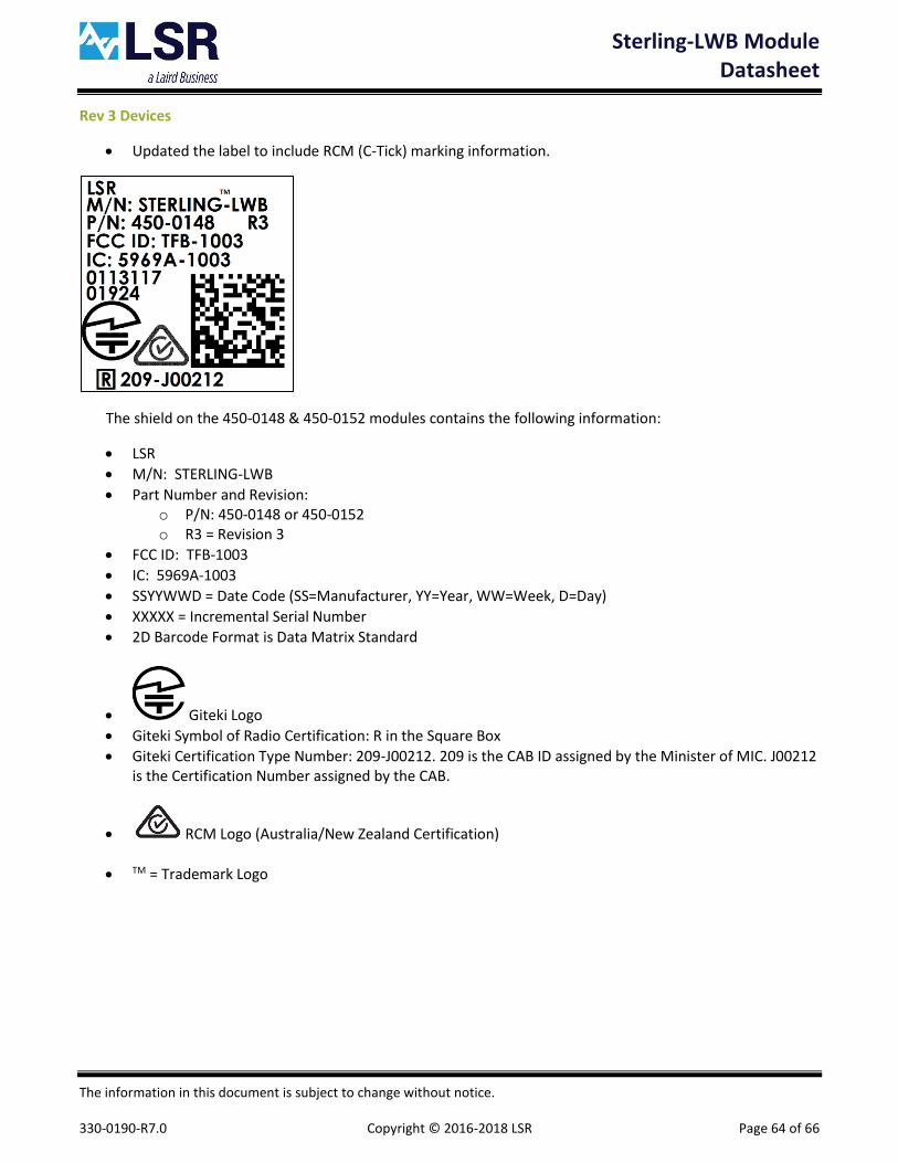
Sterling-LWB Module
Datasheet
The information in this document is subject to change without notice. 330-0190-R7.0 Copyright © 2016-2018 LSR Page 64 of 66
Rev 3 Devices
• Updated the label to include RCM (C-Tick) marking information.
The shield on the 450-0148 & 450-0152 modules contains the following information:
• LSR
• M/N: STERLING-LWB
• Part Number and Revision: o P/N: 450-0148 or 450-0152 o R3 = Revision 3
• FCC ID: TFB-1003
• IC: 5969A-1003
• SSYYWWD = Date Code (SS=Manufacturer, YY=Year, WW=Week, D=Day)
• XXXXX = Incremental Serial Number
• 2D Barcode Format is Data Matrix Standard
• Giteki Logo
• Giteki Symbol of Radio Certification: R in the Square Box
• Giteki Certification Type Number: 209-J00212. 209 is the CAB ID assigned by the Minister of MIC. J00212 is the Certification Number assigned by the CAB.
• RCM Logo (Australia/New Zealand Certification)
• TM = Trademark Logo

Sterling-LWB Module
Datasheet
The information in this document is subject to change without notice. 330-0190-R7.0 Copyright © 2016-2018 LSR Page 65 of 66
Rev 4 Devices
• Internal Update to MRP System
• All label information is the same as Rev 3

Sterling-LWB Module
Datasheet
The information in this document is subject to change without notice. 330-0190-R7.0 Copyright © 2016-2018 LSR Page 66 of 66
CONTACTING LSR
Headquarters LS Research, LLC W66 N220 Commerce Court Cedarburg, WI 53012-2636 USA Tel: (262) 375-4400 Fax: (262) 375-4248
Website www.lsr.com
Technical Support forum.lsr.com
Sales Contact [email protected]
The information in this document is provided in connection with LS Research (hereafter referred to as “LSR”) products. No license, express or implied, by estoppel or otherwise, to any intellectual property right is granted by this document or in connection with the sale of LSR products. EXCEPT AS SET FORTH IN LSR’S TERMS AND CONDITIONS OF SALE LOCATED ON LSR’S WEB SITE, LSR ASSUMES NO LIABILITY WHATSOEVER AND DISCLAIMS ANY EXPRESS, IMPLIED OR STATUTORY WARRANTY RELATING TO ITS PRODUCTS INCLUDING, BUT NOT LIMITED TO, THE IMPLIED WARRANTY OF MERCHANTABILITY, FITNESS FOR A PARTICULAR PURPOSE, OR NON-INFRINGEMENT. IN NO EVENT SHALL LSR BE LIABLE FOR ANY DIRECT, INDIRECT, CONSEQUENTIAL, PUNITIVE, SPECIAL OR INCIDENTAL DAMAGES (INCLUDING, WITHOUT LIMITATION, DAMAGES FOR LOSS OF PROFITS, BUSINESS INTERRUPTION, OR LOSS OF INFORMATION) ARISING OUT OF THE USE OR INABILITY TO USE THIS DOCUMENT, EVEN IF LSR HAS BEEN ADVISED OF THE POSSIBILITY OF SUCH DAMAGES. LSR makes no representations or warranties with respect to the accuracy or completeness of the contents of this document and reserves the right to make changes to specifications and product descriptions at any time without notice. LSR does not make any commitment to update the information contained herein. Unless specifically provided otherwise, LSR products are not suitable for, and shall not be used in, automotive applications. LSR’s products are not intended, authorized, or warranted for use as components in applications intended to support or sustain life.