low-voltage organic transistors based on tetraceno[2,3
TRANSCRIPT

Low-Voltage Organic Transistors Based onTetraceno[2,3‑b]thiophene: Contact Resistance and Air StabilityUlrike Kraft,*,†,‡ John E. Anthony,§ Emilie Ripaud,§ Marsha A. Loth,§ Edwin Weber,‡ and Hagen Klauk†
†Max Planck Institute for Solid State Research, Heisenbergstrasse 1, 70569 Stuttgart, Germany‡Technical University Bergakademie Freiberg, Leipziger Strasse 29, 09596 Freiberg, Germany§University of Kentucky, Lexington, Kentucky 40506, United States
*S Supporting Information
ABSTRACT: The small-molecule organic semiconductortetraceno[2,3-b]thiophene has been synthesized through anenvironmentally friendly synthetic route, utilizing NaBH4,rather than Al/HgCl2, for the reduction of the quinone. Low-voltage organic thin-film transistors (TFTs) have beenfabricated using tetraceno[2,3-b]thiophene and, for compar-ison, pentacene and anthradithiophene as the semiconductor.The tetraceno[2,3-b]thiophene TFTs have an effective field-effect mobility as large as 0.55 cm2 V−1 s−1 and a subthresholdswing of 0.13 V/decade. In addition, it has been found that thecontact resistance of the tetraceno[2,3-b]thiophene TFTs issubstantially smaller than that of the anthradithiophene TFTs and similar to that of the pentacene TFTs. The long-term airstability of TFTs based on all three semiconductors has been monitored over a period of 12 months. The initial charge-carriermobility of the tetraceno[2,3-b]thiophene TFTs is ∼50% smaller than that of the pentacene TFTs, but as a result of the greaterionization potential and better air stability induced by the terminal thiophene ring condensed at the thiophene-b-bond, thetetraceno[2,3-b]thiophene TFTs outperform the pentacene TFTs after continuous exposure to ambient air for just 3 months.
■ INTRODUCTION
Organic thin-film transistors (TFTs) are a promisingtechnology for the realization of flexible electronic systems,such as rollable or foldable displays or stretchable sensor arrays.The conjugated organic semiconductor that forms the activeTFT layer must meet a significant number of requirements, andto date, more than 700 different materials have been evaluatedfor this purpose.1 Pentacene was one of the first and remainsamong the most popular small-molecule semiconductors fororganic TFTs, because of its large carrier mobility.2,3 Electronicsystems that have been successfully demonstrated usingpentacene TFTs include flexible active-matrix displays,4 sensorarrays,5 radio-frequency identification (RFID) tags,6 andmicroprocessors.7
However, pentacene has a pronounced sensitivity to chemicaloxidation in ambient air8−11 that typically leads to a rapid,irreversible degradation of the electrical performance ofpentacene TFTs exposed to ambient air.12 One strategy forovercoming this problem is to replace pentacene with a materialthat has a larger ionization potential, i.e., a lower-lying highestoccupied molecular orbital (HOMO) level. This can beaccomplished, for example, by reducing the size of theconjugated core13,14 or by replacing some of the benzenerings with fused heteroaromatic rings, such as thiophene.15
This study focuses on pentacene analogues with one or bothof the terminal benzene rings replaced with thiophene ringscondensed at the thiophene-b-bond: tetraceno[2,3-b]-
thiophene16−18 and anthradithiophene.19,20 The reorganizationenergies (∼100 meV),18,21−25 the packing structure (herring-bone motif), and the lattice parameters25,26 of these semi-conductors are all similar to those of pentacene, which isbeneficial in view of efficient charge transport. Compared withpentacene, they provide better oxidation resistance, because oftheir lower-lying HOMO levels (−4.6 eV for pentacene, −4.7eV for tetraceno[2,3-b]thiophene, and −4.8 eV for anthradi-thiophene).15 To the best of our knowledge, TFTs based ontetraceno[2,3-b]thiophene and anthradithiophene have so farbeen fabricated only using thermally grown SiO2 as the gatedielectric, which is unsuitable for flexible electronics because ofthe high process temperature. In addition, in all previousreports on tetraceno[2,3-b]thiophene and anthradithiopheneTFTs, the gate dielectric was quite thick, so that the TFTs hadto be operated with relatively high voltages. Also, there are noprevious reports of the contact resistance of tetraceno[2,3-b]thiophene and anthradithiophene TFTs. Here, we present acomparison of the performance and long-term air stability ofTFTs based on tetraceno[2,3-b]thiophene, anthradithiophene,and pentacene with a gate dielectric that is obtained at asufficiently low temperature to be suitable for flexible plastic
Received: November 24, 2014Revised: January 5, 2015Published: January 5, 2015
Article
pubs.acs.org/cm
© 2015 American Chemical Society 998 DOI: 10.1021/cm5043183Chem. Mater. 2015, 27, 998−1004
substrates and is sufficiently thin that the TFTs can be operatedat voltages of 3 V.
■ EXPERIMENTAL SECTIONThe synthesis of tetraceno[2,3-b]thiophene is described in theSupporting Information. Pentacene and anthradithiophene (a mixtureof the syn and anti isomers anthra[2,3-b:7,6-b′]dithiophene andanthra[2,3-b:6,7-b′]dithiophene) were purchased from Sigma-Aldrichand used as received. n-Tetradecylphosphonic acid was purchasedfrom PCI Synthesis (Newburyport, MA).Organic thin-film transistors were fabricated on doped silicon
substrates in the staggered inverted (bottom-gate, top-contact)architecture. A 30 nm thick layer of aluminum was deposited bythermal evaporation in vacuum as a common gate electrode for allTFTs on the substrate. A ∼3.6 nm thick aluminum oxide (AlOx) layerwas generated by a brief oxygen plasma treatment.27 For the formationof the self-assembled monolayer (SAM), the substrates were immersedin a 2-propanol solution of tetradecylphosphonic acid (HC14-PA)overnight. The substrates were then rinsed with pure 2-propanol andbriefly baked on a hot plate at a temperature of 100 °C. The AlOx/SAM gate dielectric has a capacitance per unit area of 700 nF/cm228,29
(Figure S2 of the Supporting Information). A 25 nm thick layer of theorganic semiconductor (tetraceno[2,3-b]thiophene, anthradithio-phene, or pentacene) was deposited onto the AlOx/SAM gatedielectric by sublimation in vacuum. To obtain the optimal thin-filmmorphology, the substrate was held at a temperature of 60−80 °Cduring the semiconductor deposition. A 30 nm thick layer of gold wasdeposited by thermal evaporation in vacuum through a shadow maskto define the source and drain contacts. All electrical measurementswere performed in ambient air at room temperature under weakyellow laboratory light on a Micromanipulator 6200 manual probestation using an Agilent 4156C Semiconductor Parameter Analyzer.The threshold voltages and effective field-effect mobilities werecalculated from the measured transfer curves by a linear fit to the IDversus VGS data (linear regime) or the √ID versus VGS data (saturationregime). Atomic force microscopy (AFM) measurements wereperformed using a Nanoscope III Multimode instrument in tappingmode equipped with a silicon cantilever (resonance frequency of 204−497 kHz).
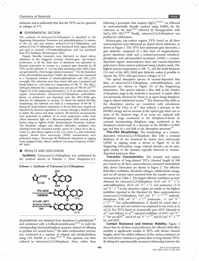
■ RESULTS AND DISCUSSIONSynthesis. Tetraceno[2,3-b]thiophene was synthesized by
the method shown in Scheme 1. First, thiophene-2,3-
dicarbaldehyde was obtained from thiophene-3-carbaldehyde30
and condensed with 1,4-dihydroxyanthracene31,32 to yield thecorresponding tetracenothiophene quinone. Instead of refluxingin pyridine for several hours,18 the aldol condensation reactionwas conducted in a mixture of ethanol and tetrahydrofuranusing 15% NaOH as a base.30,33−35 The quinone was thenreduced to tetraceno[2,3-b]thiophene. Here, rather than
following a procedure that requires HgCl2,19,36,37 we followed
an environmentally friendly method using NaBH4 for thereduction to the diol,38,39 followed by deoxygenation withSnCl2/10% HCl.34,40 Finally, tetraceno[2,3-b]thiophene waspurified by sublimation.Bottom-gate, top-contact organic TFTs based on all three
semiconductors were fabricated on doped silicon substrates, asshown in Figure 1. The TFTs have aluminum gate electrodes, agate dielectric composed of a thin layer of oxygen-plasma-grown aluminum oxide and a solution-processed tetradecyl-phosphonic acid self-assembled monolayer (SAM), a vacuum-deposited organic semiconductor layer, and vacuum-depositedgold source/drain contacts patterned using a shadow mask. Thehighest process temperature is 100 °C, and the small thickness(5.3 nm) of the AlOx/SAM gate dielectric makes it possible tooperate the TFTs with gate-source voltages of 3 V.The optical absorption spectra of vacuum-deposited thin
films of tetraceno[2,3-b]thiophene, anthradithiophene, andpentacene are shown in Figure S3 of the SupportingInformation. The spectra indicate a blue shift as the numberof thiophene rings in the molecule is increased. A similar effectwas previously observed by Payne et al. upon fusing thiophenerings to alkyne-substituted acenes.34 The observed blue shifts inthe absorption spectra are consistent with calculationsperformed by Chen et al.15 that indicate a decrease in theHOMO energy and an increase in the optical gap when one ormore of the benzene rings of an acene are replaced withthiophene rings condensed at the thiophene-b-bond. Incontrast, incorporating thiophene rings condensed at thethiophene-c-bond leads to a decrease in the HOMO−LUMOgap and thus to a red shift in the absorption spectrum.15
Thin-Film Morphology. The morphology of a vacuum-deposited tetraceno[2,3-b]thiophene film with a nominalthickness of 25 nm measured by atomic force microscopy(AFM) in tapping mode is shown in Figure S1 of theSupporting Information. Large ordered domains can be seen,quite similar to the domains typically observed in vacuum-deposited pentacene films.
Transistor Characteristics. The transfer and outputcharacteristics of long-channel TFTs (channel length of 100μm) based on all three semiconductors measured immediatelyafter device fabrication are shown in Figure 2. The effectivefield-effect mobilities, threshold voltages, subthreshold swings,and on/off current ratios extracted from the transfer curves aresummarized in Table 1. The largest effective mobilities we haveobtained for tetraceno[2,3-b]thiophene (0.55 cm2 V−1 s−1),anthradithiophene (0.14 cm2 V−1 s−1), and pentacene (1.14cm2 V−1 s−1) in the saturation regime are similar to the highestmobilities reported in the literature for these semiconductors(tetraceno[2,3-b]thiophene, 0.47 cm2 V−1 s−1;17,18 anthradi-thiophene, 0.09 cm2 V−1 s−1;19 pentacene, ∼1 cm2 V−1
s−1).41−43 For anthradithiophene, it should be noted that amixture of syn and anti isomers was employed in our work, as inref 12. For TFTs based on isomerically pure ADT, Mamada etal.25 and Nakano et al.44 reported mobilities of 0.017 cm2 V−1
s−1 for syn-ADT44 and 0.18 cm2 V−1 s−125 and 0.3 cm2 V−1 s−144
for anti-ADT.Contact Resistance and Intrinsic Mobility. Figure 3
shows that for all three semiconductors, the effective field-effectmobility is significantly smaller in TFTs with shorter channellengths, where the relative influence of the contact resistance onthe total device resistance is greater than in long-channel TFTs.By fitting the experimentally measured relationship between the
Scheme 1. Synthesis of Tetraceno[2,3-b]thiophene
Chemistry of Materials Article
DOI: 10.1021/cm5043183Chem. Mater. 2015, 27, 998−1004
999

effective field-effect mobility μeff and the channel length L tothe equation
μ =μ
+1 LL
eff0
1/2(1)
we can obtain the intrinsic channel mobility μ0 (which is thefield-effect mobility without the influence of the contacts) andthe characteristic channel length L1/2 (at which the contactresistance equals the channel resistance).45,46 The fits to thedata in Figure 3 yield intrinsic channel mobilities μ0 andcharacteristic channel lengths L1/2 of 0.31 cm2 V−1 s−1 and 6
μm for tetraceno[2,3-b]thiophene, 0.17 cm2 V−1 s−1 and 9 μmfor anthradithiophene, and 1.18 cm2 V−1 s−1 and 15 μm forpentacene, respectively (Figure 3a and Table 1).The contact resistance (and also the intrinsic channel
mobility) can be determined with the transmission line method(TLM).47−51 In a simple model, the total resistance of a field-effect transistor in the linear regime can be expressed as thesum of contact resistance RC and channel resistance Rchannel(Rtotal = RC + Rchannel). While the channel resistance isproportional to the channel length, the contact resistance isindependent of the channel length:
= +μ −
R W R WL
C V V( )total C0 diel GS th (2)
where RtotalW is the total device resistance normalized to thechannel width, RCW is the width-normalized contact resistance,L is the channel length, μ0 is the intrinsic channel mobility, Cdielis the gate-dielectric capacitance per unit area, VGS is the gate-source voltage, and Vth is the threshold voltage. In the TLManalysis, RtotalW is plotted as a function of channel length, sothat the linear fit yields RCW (by extrapolating to L = 0) andthe intrinsic channel mobility (from the slope of the linearfit)47−49 (Figure 3b).For the TLM analysis, we fabricated TFTs with channel
lengths ranging from 2 to 100 μm and measured the totalresistance at a drain-source voltage of −0.1 V (linear regime).To account for the fact that TFTs based on differentsemiconductors and/or different channel lengths may havedifferent threshold voltages, only data measured at a fixed gateoverdrive voltage [i.e., at a fixed gate-source voltage abovethreshold (VGS − Vth)] were considered for the first part of theanalysis; this assures that only contact resistances obtainedunder the same bias condition are compared.In Figure 3b, the width-normalized total resistances of TFTs
based on all three semiconductors at a gate overdrive voltage of−1.5 V are plotted as a function of channel length. The linearfits yield width-normalized contact resistances and intrinsicchannel mobilities of 1.5 kΩ cm and 0.29 cm2 V−1 s−1 fortetraceno[2,3-b]thiophene, 5.5 kΩ cm and 0.15 cm2 V−1 s−1 foranthradithiophene, and 1.4 kΩ cm and 1.14 cm2 V−1 s−1 forpentacene, respectively (Figure 3b and Table 1). These valuessuggest that there is a correlation between the contactresistance and the intrinsic mobility: When the charge carriersin the gate-induced accumulation channel have a large mobility,the contact resistance tends to be smaller. This can beunderstood in the context of the current crowdingmodel47,49,50,52 in which the semiconductor volume underneath
Figure 1. Schematic cross section of the bottom-gate, top-contact TFTs and chemical structures of the three organic semiconductors investigated inthis study (tetraceno[2,3-b]thiophene, anthradithiophene, and pentacene).
Figure 2. Transfer characteristics in the linear (VDS = −0.1 V) andsaturation (VDS = −1.5 V) regime and output characteristics of freshtetraceno[2,3-b]thiophene, anthradithiophene, and pentacene TFTs.
Chemistry of Materials Article
DOI: 10.1021/cm5043183Chem. Mater. 2015, 27, 998−1004
1000

Table 1. Maximal and Average Effective Field-Effect Mobilities, Threshold Voltages, Subthreshold Swings, and On/Off CurrentRatios of Tetraceno[2,3-b]thiophene, Anthradithiophene, and Pentacene TFTs with a Channel Length of 100 μm in theSaturation Regime and in the Linear Regime, and Intrinsic Channel Mobilities and Width-Normalized Contact ResistancesExtracted using TLM (from Figure 3)
tetraceno[2,3-b]thiophene anthradithiophene pentacene
Saturation Regime (VDS = −1.5 V; L = 100 μm)maximal effective field-effect mobility 0.55 cm2 V−1 s−1 0.14 cm2 V−1 s−1 1.14 cm2 V−1 s−1
average effective field-effect mobility 0.41 ± 0.07 cm2 V−1 s−1 0.13 ± 0.005 cm2 V−1 s−1 0.99 ± 0.17 cm2 V−1 s−1
threshold voltage −1.37 ± 0.15 V −1.11 ± 0.15 V −1.22 ± 0.07 Vsubthreshold swing 168 ± 18 mV/decade 243 ± 20 mV/decade 132 ± 6 mV/decadeon/off current ratio 105 104 106
Linear Regime (VDS = −0.1 V; L = 100 μm)maximal effective field-effect mobility 0.42 cm2 V−1 s−1 0.12 cm2 V−1 s−1 1.26 cm2 V−1 s−1
average effective field-effect mobility 0.35 ± 0.06 cm2 V−1 s−1 0.10 ± 0.01 cm2 V−1 s−1 1.05 ± 0.19 cm2 V−1 s−1
threshold voltage −1.47 ± 0.13 V −1.45 ± 0.01 V −1.33 ± 0.06 Vsubthreshold swing 128 ± 60 mV/decade 308 ± 30 mV/decade 145 ± 6 mV/decadeon/off current ratio 104 103 105
Fit to μeff = f(L)intrinsic mobility (μ0) 0.31 ± 0.005 cm2 V−1 s−1 0.17 ± 0.006 cm2 V−1 s−1 1.18 ± 0.035 cm2 V−1 s−1
L1/2 5.5 ± 0.38 μm 8.8 ± 1.3 μm 15 ± 1.6 μmTransmission Line Method (VGS − Vth = −1.5 V; VDS = −0.1 V)
intrinsic mobility (μ0) 0.29 ± 0.004 cm2 V−1 s−1 0.15 ± 0.006 cm2 V−1 s−1 1.14 ± 0.037 cm2 V−1 s−1
width-normalized contact resistance 1.5 ± 0.15 kΩ cm 5.5 ± 1.2 kΩ cm 1.4 ± 0.15 kΩ cm
Figure 3. (a) Effective field-effect mobility in the linear regime as a function of channel length. The fit to eq 1 yields intrinsic channel mobility μ0. (b)Transmission line method (TLM). Channel width-normalized total resistance as a function of channel length. All resistances were measured at afixed overdrive voltage (VGS − Vth) of −1.5 V and a drain-source voltage of −0.1 V. Extrapolation to a channel length of zero yields the width-normalized contact resistance RCW, and the inverse of the slope of the linear fit yields the intrinsic channel mobility μ0. (c) Channel width-normalized contact resistance (RCW) as a function of inverse gate overdrive voltage.
Chemistry of Materials Article
DOI: 10.1021/cm5043183Chem. Mater. 2015, 27, 998−1004
1001
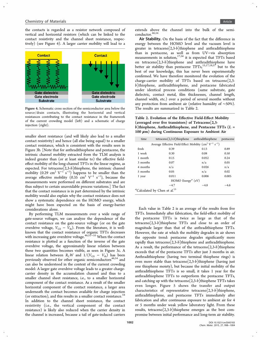
the contacts is regarded as a resistor network composed ofvertical and horizontal resistors (which can be linked to thecontact resistivity and the channel sheet resistance, respec-tively) (see Figure 4). A larger carrier mobility will lead to a
smaller sheet resistance (and will likely also lead to a smallercontact resistivity) and hence (all else being equal) to a smallercontact resistance, which is consistent with the results seen inFigure 3b. [Note that for anthradithiophene and pentacene, theintrinsic channel mobility extracted from the TLM analysis isindeed greater than (or at least similar to) the effective field-effect mobility of the long-channel TFTs in the linear regime, asexpected. For tetraceno[2,3-b]thiophene, the intrinsic channelmobility (0.29 cm2 V−1 s−1) happens to be smaller than theaverage effective mobility (0.35 cm2 V−1 s−1), because themeasurements were performed on different substrates and arethus subject to certain unavoidable process variations.] The factthat the contact resistance is in part determined by the intrinsicmobility would also explain why the contact resistance does notshow a systematic dependence on the HOMO energy, whichmight have been expected on the basis of energy-barrierconsiderations alone.By performing TLM measurements over a wide range of
gate-source voltages, we can analyze the dependence of thecontact resistance on the gate-source voltage (or on the gateoverdrive voltage, VGS − Vth). From the literature, it is well-known that the contact resistance of organic TFTs decreaseswith increasing gate overdrive voltage.46,51−55 When the contactresistance is plotted as a function of the inverse of the gateoverdrive voltage, the approximately linear relation betweenthese two quantities becomes visible, as seen in Figure 3c. Alinear relation between RCW and 1/(VGS − Vth) has beenpreviously observed for other organic semiconductors46,54 andcan also be understood in the context of the current crowdingmodel: A larger gate overdrive voltage leads to a greater charge-carrier density in the accumulation channel and thus to asmaller channel sheet resistance, i.e., to a smaller horizontalcomponent of the contact resistance. As a result of the smallerhorizontal component of the contact resistance, a larger areaunderneath the contact becomes available for charge injection(or extraction), and this results in a smaller contact resistance.54
In addition to the channel sheet resistance, the contactresistivity (i.e., the vertical component of the contactresistance) is likely also reduced when the carrier density inthe channel is increased, because a tail of gate-induced carriers
extends above the channel into the bulk of the semi-conductor.46,54
Air Stability. On the basis of the fact that the difference inenergy between the HOMO level and the vacuum level isgreater in tetraceno[2,3-b]thiophene and anthradithiophenethan in pentacene, as well as from UV−vis absorptionmeasurements in solution,17,56 it is expected that TFTs basedon tetraceno[2,3-b]thiophene and anthradithiophene havebetter air stability than pentacene TFTs,15,17,18,57 but to thebest of our knowledge, this has never been experimentallyconfirmed. We have therefore monitored the evolution of thecharge-carrier mobility of TFTs based on tetraceno[2,3-b]thiophene, anthradithiophene, and pentacene fabricatedunder identical process conditions (same substrate, gatedielectric, contact metal, film thicknesses, channel length,channel width, etc.) over a period of several months withoutany protection from ambient air (relative humidity of ∼50%).The results are summarized in Table 2.
Each value in Table 2 is an average of the results from fiveTFTs. Immediately after fabrication, the field-effect mobility ofthe pentacene TFTs is twice as large as that of thetetraceno[2,3-b]thiophene TFTs and close to an order ofmagnitude larger than that of the anthradithiophene TFTs.However, the rate at which the mobility degrades in air showsthe opposite trend: pentacene degrades significantly morerapidly than tetraceno[2,3-b]thiophene and anthradithiophene.As a result, the performance of the tetraceno[2,3-b]thiopheneexceeds that of the pentacene TFTs after just 3 months in air.Anthradithiophene (having two terminal thiophene rings) iseven more stable than tetraceno[2,3-b]thiophene (having justone thiophene moiety), but because the initial mobility of theanthradithiophene TFTs is so small, it takes 1 year for theanthradithiophene TFTs to outperform the pentacene TFTs,and catching up with the tetraceno[2,3-b]thiophene TFTs takeseven longer. Figure 5 shows the transfer and outputcharacteristics of representative tetraceno[2,3-b]thiophene,anthradithiophene, and pentacene TFTs immediately afterfabrication and after continuous exposure to ambient air for 4or 5 months under weak yellow laboratory light. From theseresults, tetraceno[2,3-b]thiophene emerges as the best com-promise between initial performance and long-term air stability.
Figure 4. Schematic cross section of the semiconductor area below thesource/drain contacts, illustrating the horizontal and verticalresistances contributing to the contact resistance in the frameworkof the current crowding model (left) and a schematic of chargeinjection (right).
Table 2. Evolution of the Effective Field-Effect Mobility(averaged over five transistors) of Tetraceno[2,3-b]thiophene, Anthradithiophene, and Pentacene TFTs (L =100 μm) during Continuous Exposure to Ambient Air
time tetraceno[2,3-b]thiophene anthradithiophene pentacene
Average Effective Field-Effect Mobility (cm2 V−1 s−1)fresh 0.39 0.13 0.891 week 0.30 0.08 0.501 month 0.15 0.052 0.243 months 0.07 n/a 0.054 months n/a 0.026 n/a5 months 0.05 n/a 0.021 year 0.011 0.006 0.005
HOMO Energya (eV)−4.7 −4.8 −4.6
aCalculated by Chen et al.15
Chemistry of Materials Article
DOI: 10.1021/cm5043183Chem. Mater. 2015, 27, 998−1004
1002

■ CONCLUSIONS
In summary, the small-molecule organic semiconductortetraceno[2,3-b]thiophene was synthesized, utilizing NaBH4,rather than the more toxic Al/HgCl2, for the reduction of thequinone. Low-voltage organic TFTs based on a low-temper-ature-processed ultrathin gate dielectric were fabricated usingtetraceno[2,3-b]thiophene and, for comparison, pentacene andanthradithiophene as the semiconductor. In addition to theeffective field-effect mobility extracted from the transfercharacteristics, the contact resistance and the intrinsic channelmobility were also determined by employing the transmissionline method on TFTs with channel lengths ranging from 2 to100 μm. The contact resistance of the tetraceno[2,3-b]-thiophene TFTs was found to be similar to that of thepentacene TFTs and substantially smaller than that of theanthradithiophene TFTs. The long-term air stability of TFTsbased on all three semiconductors was monitored over a periodof 12 months. The initial carrier mobility of the tetraceno[2,3-b]thiophene TFTs is ∼50% smaller than that of the pentaceneTFTs, but as a result of the greater ionization potential andbetter air stability induced by the terminal thiophene ringcondensed at the thiophene-b-bond, the tetraceno[2,3-b]-thiophene TFTs outperform the pentacene TFTs aftercontinuous exposure to ambient air for just 3 months.
■ ASSOCIATED CONTENT
*S Supporting InformationExperimental procedures, synthesis, and absorption spectra.This material is available free of charge via the Internet athttp://pubs.acs.org.
■ AUTHOR INFORMATION
Corresponding Author*E-mail: [email protected].
NotesThe authors declare no competing financial interest.
■ ACKNOWLEDGMENTS
This work was partially funded by the German ResearchFoundation (DFG) under Grants KL 2223/5-1 and KL 2223/5-2.
■ REFERENCES(1) Wang, C.; Dong, H.; Hu, W.; Liu, Y.; Zhu, D. Chem. Rev. 2011,112, 2208.(2) Kelley, T. W.; Boardman, L. D.; Dunbar, T. D.; Muyres, D. V.;Pellerite, M. J.; Smith, T. P. J. Phys. Chem. B 2003, 107, 5877.(3) Wei, C.-Y.; Kuo, S.-H.; Huang, W.-C.; Hung, Y.-M.; Yang, C.-K.;Adriyanto, F.; Wang, Y.-H. IEEE Trans. Electron Devices 2012, 59, 477.
Figure 5. Electrical performance of the tetraceno[2,3-b]thiophene, anthradithiophene, and pentacene TFTs (L = 100 μm) directly after fabricationand after continuous exposure to ambient air for several months. After a few months in air, the tetraceno[2,3-b]thiophene TFTs outperform thepentacene TFTs, because of their better air stability.
Chemistry of Materials Article
DOI: 10.1021/cm5043183Chem. Mater. 2015, 27, 998−1004
1003

(4) Yagi, I.; Hirai, N.; Miyamoto, Y.; Noda, M.; Imaoka, A.; Yoneya,N.; Nomoto, K.; Kasahara, J.; Yumoto, A.; Urabe, T. J. Soc. Inf. Disp.2008, 16, 15.(5) Someya, T.; Kato, Y.; Sekitani, T.; Iba, S.; Noguchi, Y.; Murase,Y.; Kawaguchi, H.; Sakurai, T. Proc. Natl. Acad. Sci. U.S.A. 2005, 102,12321.(6) Myny, K.; Steudel, S.; Smout, S.; Vicca, P.; Furthner, F.; van derPutten, B.; Tripathi, A. K.; Gelinck, G. H.; Genoe, J.; Dehaene, W. Org.Electron. 2010, 11, 1176.(7) Myny, K.; van Veenendaal, E.; Gelinck, G. H.; Genoe, J.;Dehaene, W.; Heremans, P. IEEE J. Solid-State Circuits 2012, 47, 284.(8) Reddy, A. R.; Bendikov, M. Chem. Commun. 2006, 1179.(9) Maliakal, A.; Raghavachari, K.; Katz, H.; Chandross, E.; Siegrist,T. Chem. Mater. 2004, 16, 4980.(10) Thorley, K. J.; Anthony, J. E. Isr. J. Chem. 2014, 54, 642.(11) Adam, W.; Prein, M. Acc. Chem. Res. 1996, 29, 275.(12) Pannemann, C.; Diekmann, T.; Hilleringmann, U. J. Mater. Res.2004, 19, 1999.(13) Meng, H.; Sun, F.; Goldfinger, M. B.; Jaycox, G. D.; Li, Z.;Marshall, W. J.; Blackman, G. S. J. Am. Chem. Soc. 2005, 127, 2406.(14) Meng, H.; Sun, F.; Goldfinger, M. B.; Gao, F.; Londono, D. J.;Marshal, W. J.; Blackman, G. S.; Dobbs, K. D.; Keys, D. E. J. Am.Chem. Soc. 2006, 128, 9304.(15) Chen, Y.; Shen, L.; Li, X. J. Phys. Chem. A 2014, 118, 5700.(16) Bailey, D.; Levy, D.; Mai, X.; Scuderi, A. U.S. Patent20060220007, 2005.(17) Tang, M. L.; Okamoto, T.; Bao, Z. J. Am. Chem. Soc. 2006, 128,16002.(18) Valiyev, F.; Hu, W.-S.; Chen, H.-Y.; Kuo, M.-Y.; Chao, I.; Tao,Y.-T. Chem. Mater. 2007, 19, 3018.(19) Laquindanum, J. G.; Katz, H. E.; Lovinger, A. J. J. Am. Chem.Soc. 1998, 120, 664.(20) Chen, M.-C.; Kim, C.; Chen, S.-Y.; Chiang, Y.-J.; Chung, M.-C.;Facchetti, A.; Marks, T. J. J. Mater. Chem. 2008, 18, 1029.(21) Takimiya, K.; Shinamura, S.; Osaka, I.; Miyazaki, E. Adv. Mater.2011, 23, 4347.(22) Kwon, O.; Coropceanu, V.; Gruhn, N.; Durivage, J.;Laquindanum, J.; Katz, H.; Cornil, J.; Bredas, J.-L. J. Chem. Phys.2004, 120, 8186.(23) Kuo, M.-Y.; Liu, C.-C. J. Phys. Chem. C 2009, 113, 16303.(24) Arulmozhiraja, S.; Ohno, T. J. Phys. Chem. C 2008, 112, 16561.(25) Mamada, M.; Katagiri, H.; Mizukami, M.; Honda, K.; Minamiki,T.; Teraoka, R.; Uemura, T.; Tokito, S. ACS Appl. Mater. Interfaces2013, 5, 9670.(26) Yuan, Q.; Mannsfeld, S. C. B.; Tang, M. L.; Toney, M. F.;Luning, J.; Zhenan, B. J. Am. Chem. Soc. 2008, 130, 3502.(27) Klauk, H.; Zschieschang, U.; Pflaum, J.; Halik, M. Nature 2007,445, 745.(28) Salinas, M.; Jager, C. M.; Amin, A. Y.; Dral, P. O.; Meyer-Friedrichsen, T.; Hirsch, A.; Clark, T.; Halik, M. J. Am. Chem. Soc.2012, 134, 12648.(29) Zschieschang, U.; Ante, F.; Schlorholz, M.; Schmidt, M.; Kern,K.; Klauk, H. Adv. Mater. 2010, 22, 4489.(30) De la Cruz, P.; Martin, N.; Miguel, F.; Seoane, C.; Albert, A.;Cano, F. H.; Gonzalez, A.; Pingarron, J. M. J. Org. Chem. 1992, 57,6192.(31) Chen, Z.; Amara, J. P.; Thomas, S. W.; Swager, T. M.Macromolecules 2006, 39, 3202.(32) Hua, D. H.; Tamura, M.; Huang, X.; Stephany, H. A.; Helfrich,B. A.; Perchellet, E. M.; Sperfslage, B. J.; Perchellet, J.-P.; Jiang, S.;Kyle, D. E.; Chiang, P. K. J. Org. Chem. 2002, 67, 2907.(33) Ried, W.; Anthofer, F. Angew. Chem. 1953, 65, 601.(34) Payne, M. M.; Odom, S. A.; Parkin, S. R.; Anthony, J. E. Org.Lett. 2004, 6, 3325.(35) Anthony, J. E.; Gierschner, J.; Landis, C. A.; Parkin, S. R.;Sherman, J. B.; Bakus, R. C., II. Chem. Commun. 2007, 4746.(36) Goodings, E.; Mitchard, D.; Owen, G. J. Chem. Soc., PerkinTrans. 1 1972, 1310.
(37) Park, S. K.; Jackson, T. N.; Anthony, J. E.; Mourey, D. A. Appl.Phys. Lett. 2007, 91, 063514.(38) Kuninobu, Y.; Seiki, T.; Kanamaru, S.; Nishina, Y.; Takai, K.Org. Lett. 2010, 12, 5287.(39) Pramanik, C.; Miller, G. P. Molecules 2012, 17, 4625.(40) Anthony, J. E.; Subramanian, S.; Parkin, S. R.; Park, S. K.;Jackson, T. N. J. Mater. Chem. 2009, 19, 7984.(41) Okamoto, T.; Senatore, M. L.; Ling, M.-M.; Mallik, A. B.; Tang,M. L.; Bao, Z. Adv. Mater. 2007, 19, 3381.(42) Wang, C.-H.; Jian, S.-D.; Chan, S.-W.; Ku, C.-S.; Huang, P.-Y.;Chen, M.-C.; Yang, Y.-W. J. Phys. Chem. C 2012, 116, 1225.(43) Kraft, U.; Zschieschang, U.; Ante, F.; Kalblein, D.; Kamella, C.;Amsharov, K.; Jansen, M.; Kern, K.; Weber, E.; Klauk, H. J. Mater.Chem. 2010, 20, 6416.(44) Nakano, M.; Niimi, K.; Miyazaki, E.; Osaka, I.; Takimiya, K. J.Org. Chem. 2012, 77, 8099.(45) Marinkovic, M.; Belaineh, D.; Wagner, V.; Knipp, D. Adv. Mater.2012, 24, 4005.(46) Rodel, R.; Letzkus, F.; Zaki, T.; Burghartz, J.; Kraft, U.;Zschieschang, U.; Kern, K.; Klauk, H. Appl. Phys. Lett. 2013, 102,233303.(47) Berger, H. J. Electrochem. Soc. 1972, 119, 507.(48) Ante, F.; Kalblein, D.; Zaki, T.; Zschieschang, U.; Takimiya, K.;Ikeda, M.; Sekitani, T.; Someya, T.; Burghartz, J. N.; Kern, K.; Klauk,H. Small 2012, 8, 73.(49) Schroder, D. K. Semiconductor Material and Device Character-ization; Wiley: Hoboken, NJ, 2008.(50) Chiang, C.-S.; Martin, S.; Kanicki, J.; Ugai, Y.; Yukawa, T.;Takeuchi, S. Jpn. J. Appl. Phys. 1998, 37, 5914.(51) Gundlach, D.; Zhou, L.; Nichols, J.; Jackson, T.; Necliudov, P.;Shur, M. J. Appl. Phys. 2006, 100, 024509.(52) Natali, D.; Caironi, M. Adv. Mater. 2012, 24, 1357.(53) Kraft, U.; Sejfic, M.; Kang, M. J.; Takimiya, K.; Zaki, T.; Letzkus,F.; Burghartz, J. N.; Weber, E.; Klauk, H. Adv. Mater. 2015, 27, 207−214.(54) Richards, T.; Sirringhaus, H. J. Appl. Phys. 2007, 102, 094510.(55) Zaumseil, J.; Baldwin, K. W.; Rogers, J. A. J. Appl. Phys. 2003,93, 6117.(56) Mei, J.; Diao, Y.; Appleton, A. L.; Fang, L.; Bao, Z. J. Am. Chem.Soc. 2013, 135, 6724.(57) Tylleman, B. T.; Vande Velde, C. M.; Balandier, J.-Y.; Stas, S.;Sergeyev, S.; Geerts, Y. H. Org. Lett. 2011, 13, 5208.
■ NOTE ADDED AFTER ASAP PUBLICATIONThis article was published ASAP on January 16, 2015, with aminor text error in the Conclusions section. The correctedversion was published ASAP on January 20, 2015.
Chemistry of Materials Article
DOI: 10.1021/cm5043183Chem. Mater. 2015, 27, 998−1004
1004

1
Supporting Information
Low-voltage Organic Transistors Based on Tetraceno[2,3-b]thiophene: Contact Resistance and Air Stability
Ulrike Kraft, *, †,§ John E. Anthony,⊥ Emilie Ripaud,⊥ Marsha A. Loth,⊥
Edwin Weber,§ Hagen Klauk†
† Max Planck Institute for Solid State Research, Heisenbergstr. 1, 70569 Stuttgart, Germany
(email: [email protected], phone: +49 711 689 1340) § Technical University Freiberg, Leipziger Str. 29, 09596 Freiberg, Germany
⊥ University of Kentucky, Lexington, KY 40506-005, USA
1. General procedures 2. Synthesis 3. Semiconductor thin-film morphology 4. Gate-dielectric capacitance measurements 5. Absorption spectra 6. Additional references
2
1. General procedures 1H and 13C NMR spectra were recorded with a Varian Unity (400 MHz) spectrometer. Proton chemical shifts were referenced to CDCl3 (7.27 ppm) and to DMSO (2.5 ppm); 13C shifts were referenced to CDCl3 (77.0 ppm) and to DMSO (39.51 ppm). The multiplicities are labeled by s (singlet), d (doublet), t (triplet), m (multiplet), dd (doublet of doublets). Mass spectra were recorded either using a JEOL JMS-700T in EI mode (70 eV) or a MALDI-TOF-MS Axima Resonance from Shimadzu in LDI-MS mode (laser desorption ionization-mass spectrometry). Absorption Spectra were recorded using a Lambda 9 Spectrometer from Perkin-ELMER in transmission configuration. Sample preparation: Organic thin-film transistors were fabricated in the staggered inverted (bottom-gate, top-contact) architecture on doped silicon substrates. Aluminum gate electrodes with a thickness of 30 nm were deposited onto the substrates by thermal evaporation in vacuum. A ~3.6 nm thick aluminum oxide layer was generated by a brief oxygen plasma treatment (30 sccm O2, 10 mTorr, 200 W, 30 s). For the formation of the self-assembled monolayer (SAM), the substrates were immersed overnight into a 2-propanol solution with a concentration of ~1 to 2 mmol/l of n-tetradecylphosphonic acid (HC14-PA) at room temperature. The substrates were then rinsed with pure 2-propanol and annealed on a hotplate at a temperature of 100 °C for about 10 min. The quality of the SAMs was confirmed by static contact angle measurements. The AlOx/SAM gate dielectrics have a capacitance per unit area of 0.7 µF/cm2 (28,29) (see Figure S2). A nominally 25 nm thick layer of the organic semiconductor was deposited onto the AlOx/SAM gate dielectric by sublimation in vacuum. During the semiconductor deposition, the substrate was held at a temperature of 70°C for tetraceno[2,3-b]thiophene, 80°C for anthradithiophene and 60°C for pentacene, since this was found to provide the largest field-effect mobility for each semiconductor. The TFTs were completed by the vacuum deposition of gold source and drain contacts. All vacuum depositions were carried out with a Leybold UNIVEX 300 vacuum system at a base pressure of about 10-6 mbar. The film thickness was measured with a quartz crystal microbalance. Aluminum was deposited with a deposition rate of ~9-12 Å/s, the organic semiconductor and the gold contacts were deposited with a deposition rate of 0.2-0.3 Å/s. Electrical measurements were carried out on a vibration-damped Micromanipulator 6200 probe station with an Agilent 4156C Semiconductor Parameter Analyzer. The measurements were performed in ambient air (humidity ~ 50 %) at room temperature and under yellow lab light. The effective field-effect mobilities and threshold voltages were calculated from the measured transfer curves using a linear fit to the ID versus VGS data in the linear regime and to the √ID versus VGS data in the saturation regime. The values given in Table 1 are for the mean and the standard deviation of parameters obtained from 7 tetraceno[2,3-b]thiophene TFTs (4 substrates), 4 anthradithiophene TFTs (1 substrate) and 7 pentacene TFTs (5 substrates). During the air-stability tests, the substrates were stored over a period of several months without protection from ambient air (relative humidity ~50 %) and without protection from the weak yellow laboratory light. Atomic force microscopy (AFM) was conducted with a Nanoscope III Multimode in tapping mode with silicon cantilevers (resonance frequency: 204-497 kHz) and were processed with WSxM.[S1]
3
2. Synthesis 1,4-Anthracenedione [S2]
5.1 g of sodium borohydride (133 mmol, 4 eq) was added in small portions to an ice-cooled (0°C) stirred solution of 8.0 g (33 mmol) quinizarin (1,4-dihydroxyanthraquinone) in 150 ml methanol under nitrogen atmosphere. The reaction was monitored by working up an aliquot of the reaction mixture and checking for the disappearance of quinizarin by TLC. The mixture was stirred overnight and cooled with an ice bath before quenching slowly with 6N hydrochloric acid (90 ml). The crude product was filtered, washed with water, dried under reduced pressure and purified with a dry silica plug using 1:1 hexanes/DCM first and then DCM to give 6.5 g (94 %) of orange crystals. 1H-NMR (400 MHz, CDCl3): δ 7.08 (s, 2H, ArH); 7.71 (m, 2H, ArH); 8.08 (m, 2H, ArH), 8.64 (s, 2H, ArH) ppm. 13C-NMR (100 MHz, CDCl3): δ 128.35; 128.87, 129.59, 130.22, 134.82, 140.06, 184.68 ppm. 1,4-Dihydroxyanthracene [S2,S3]
A mixture of 300 ml of dioxane and 100 ml of water was purged with nitrogen for 1 h and then added to a flame-dried, nitrogen-cooled 100 ml RBF. After adding 3.34 g (19 mmol) of sodium dithionite (Na2S2O4) and degassing for another 30 min, 1.0 g (4.8 mmol) of 1,4 anthracenedione was added and the mixture was stirred under nitrogen flow. After the addition of another 1.25 g (7 mmol) of Na2S2O4, the mixture was stirred overnight under nitrogen flow at room temperature. The reaction mixture was then poured into 100 ml of nitrogen-purged water that was cooled with an ice bath. After filtering under nitrogen flow, the product was dried under reduced pressure to give 0.79 g (78 %) of a yellow powder. 1H-NMR (400 MHz, DMSO-d6): δ 6.62 (s, 2H, ArH); 7.46 (m, 2H, J1 = 6.4 Hz, J2 = 3.3 Hz ArH); 8.08 (m, 2H, J1 = 6.5 Hz, J2 = 3.4 Hz, ArH) ppm;. 8.67 (s, 2H, ArH); 9.56 (s, 2H, OH) ppm. 13C-NMR (100 MHz, DMSO-d6): δ 105.51, 120.58, 125.25, 128.34, 130.44, 145.34 ppm.
4
Thiophene-3-aldehyde ethylene acetal [S4]
A 250 ml round bottom flask was charged with 25 g (223 mmol) 3-thiophenecarbaldehyde dissolved in 100 ml of benzene, 15 ml (16.65 g, 268 mmol) of ethylene glycol and a catalytic amount of camphor sulfonic acid. The flask was equipped with a Dean-Stark trap and a reflux condenser to collect the water formed during the reaction, and the reaction mixture was kept at a temperature of 111°C overnight. After cooling to room temperature, the mixture was poured into 100 ml of saturated aqueous sodium bicarbonate solution (NaHCO3) and stirred at room temperature for 30 min. The aqueous phase was then extracted 5 times with diethyl ether and the combined organic layers were dried with MgSO4 and filtered. The solvents were removed under reduced pressure to give 34.4 g (99 %) of a brown oil. 1H NMR (400 MHz, CDCl3): δ 3.95 (m, 4H); 5.88 (s, 1H); 7.18 (d, J = 5.2 Hz, 1H); 7.28 (d, J = 4.6 Hz, 1H); 7.40 (s, 1H) ppm. 13C NMR (50 MHz, CDCl3): δ 64.91, 100.39, 123.58, 125.76, 126.19, 140.38 ppm. MS (EI 70 eV) m/z = 156 (M+), 84 (M+ -C3H5O2). Thiophene-2,3-dicarbaldehyde
A flame-dried 250 ml round bottom flask was charged with 15.6 g (100 mmol) of thiophene-3-carbaldehyde ethylene acetal that was dissolved in 100 ml of anhydrous tetrahydrofuran (THF) under nitrogen atmosphere. The reaction mixture was cooled to -78°C under nitrogen. 40 ml (100 mmol) of a 2.5 M solution of n‐butyllithium in hexanes was then added slowly with a syringe. The mixture was stirred at -78°C for 15 min, whereupon 22 ml (25.19 g, 218 mmol) of N-formylmorpholine was added with a syringe. The solution was stirred and allowed to warm up to room temperature overnight. After quenching with water, the reaction mixture was extracted with diethyl ether, dried with MgSO4, filtered and concentrated under reduced pressure. The material was eluted through a silica gel plug (2:1 hexanes/ethyl acetate), then dissolved in 100 ml of 80 % acetic acid and kept at a temperature of 60°C overnight. After cooling to room temperature, 100 ml of ethyl acetate and 500 ml of water were added. Subsequently, the organic layer was separated from the aqueous layer, washed with water, dried with MgSO4 and filtered. The solvents were removed under reduced pressure. The crude product was eluted through a silica gel plug (5:1 hexanes/ ethyl acetate), and recrystallized in hexanes to give 7.6 g (54 %) of fluffy yellowish crystals. 1H-NMR (400 MHz, CDCl3): δ 7.62 (d, 1H, J = 5.1 Hz, ArH); 7.72 (dd, 1H, J1 = 5.1 Hz, J2 = 1.2 Hz, ArH); 10.36 (s, 1H, CHO); 10.46 (d, 1H, J = 0.8 Hz, CHO) ppm. 13C-NMR (100 MHz, CDCl3): δ 130.06, 133.90, 143.58, 147.24, 182.70, 184.72 ppm. MS (EI 70 eV) m/z = 140 (M+), 111 (M+ -CHO).
5
Tetraceno[2,3-b]thiophene-5,12-dione
0.98 g (7 mmol) of thiophene-2.3-dicarbaldehyde and 1.46 g (7 mmol) of 1,4-dihydroxyanthracene were added to a 250 ml round bottom flask equipped with a stir bar and were dissolved in a hot mixture of 10 ml of THF and 5 ml of ethanol. A few drops of 15% aqueous NaOH solution were then added while stirring until a precipitate was observed. The slurry was stirred for one hour and was subsequently filtered through a Büchner funnel, washed with methanol until the filtrate was colorless, followed by THF and diethyl ether (in this sequence) to give 1.6 g (72 %) of an off-white solid. 1H-NMR (400 MHz, CDCl3): δ 7.63 (d, 1H, J = 5.27 Hz, ArH); 7.72 (dd, 2H, J1 = 6.4 Hz, J2 = 3.3 H, ArH); 7.81 (d, 1H, J = 5.71 Hz, ArH); 8.14 (dd, 2H, J1 = 6.4 Hz, J2 = 3.3 Hz, ArH); 8.89 (s, 1H,ArH); 8.93(s, 2H, ArH); 8.97(s, 2H, ArH) ppm. Tetraceno[2,3-b]thiophene [39]
In a flame-dried 500 ml round bottom flask equipped with a stir bar, 1.0 g (3.18 mmol) of tetraceno[2,3-b]thiophenequinone was dissolved in 60 ml of anhydrous THF. Then, 1.2 g (31.85 mmol, 10 eq) of sodium borohydride was added and the reaction mixture was heated at 60°C for several days until TLC followed by SnCl2/HCl treatment revealed that the reaction was complete. 10 % hydrochloric acid and 3.59 g (15.9 mmol, 5 eq) of stannous chloride (SnCl2) was added. After stirring for 1 h, the mixture was filtered in the dark under nitrogen flow and washed with degassed methanol to give 0.74 g (82 %) of a purple powder. MS (LDI-MS) m/z = 284.06 (M+, 100%).

6
3. Semiconductor thin-film morphology
Figure S1. Semiconductor thin-film morphology: Topography (left) and amplitude (right) images of a tetraceno[2,3-b]thiophene thin-film with a nominal thickness of 25 nm measured by atomic force microscopy (AFM) in tapping mode. The images are from the same sample, showing two different magnifications.
4. Gate-dielectric capacitance measurements
Figure S2. Capacitance per unit area of the AlOx/SAM gate dielectric as a function of frequency. The capacitance was measured on Al/AlOx/SAM/Au test structures with shadow-mask patterned Al bottom electrodes and Au top electrodes fabricated on a thermally oxidized silicon wafer. Inset: A photograph of one of the test structure with an overlap area of 200 �m x 200 �m.
100 µm100 µm

7
5. Absorption spectra
Figure S3. Absorbance of 25 nm thick, vacuum-deposited thin films of anthradithiophene (1), tetraceno[2,3-b]thiophene (2) and pentacene (3).
6. Additional references S1. Horcas, I.; Fernández, R.; Gómez-Rodríguez, J. M.; Colchero, J.; Gómez-Herrero, J.;
Baro, A. M., WSXM: A software for scanning probe microscopy and a tool for nanotechnology, Review of Scientific Instruments 2007, 78, 013705.
S2. Hua, D. H.; Tamura, M.; Huang, X.; Stephany, H. A.; Helfrich, B. A.; Perchellet, E. M.; Sperfslage, B. J.; Perchellet, J.-P.; Jiang, S.; Kyle, D. E., Chiang, P. K., Syntheses and bioactivities of substituted 9, 10-dihydro-9, 10-[1, 2] benzenoanthracene-1, 4, 5, 8-tetrones. Unusual reactivities with amines, J. Org. Chem. 2002, 67, 2907.
S3. Chen, Z.; Amara, J. P.; Thomas, S. W.; Swager, T. M., Synthesis of a novel poly (iptycene) ladder polymer, Macromolecules 2006, 39, 3202.
S4. De la Cruz, P.; Martin, N.; Miguel, F.; Seoane, C.; Albert, A.; Cano, F. H.; Gonzalez, A.; Pingarron, J. M., Novel pi-extended thiophene-fused electron acceptors for organic metals, J. Org. Chem. 1992, 57, 6192.