low power design in layout and system level · low power design in layout and system level qian,...
TRANSCRIPT

Low Power Design in Layout and
System Level
Q I A N , z a i c h e n
A Thesis Submitted in Partial Fulfilment
of the Requirements for the Degree of
Master of Philosophy
in
Computer Science and Engineering
The Chinese University of Hong Kong
March 2010


Thesis/Assessment Committee
Professor WU Yu Liang David (Chair)
Professor YOUNG Fung Yu (Thesis Supervisor)
Professor XU Qiang ( Committee Member)
Professor Wai-Kei Mak (External Examiner)

Abstract
A lot of attention has been paid to low-power IC design today, and power con-
sumption has become an important, if not the most critical, issue in system-on-chip
(SoC) design. While progress has been made, much more remains to be done to
automate the low-power design and verification flow, at different levels of abstrac-
tion. In this thesis, we will address several problems in low power design at both
the physical and system design levels.
in the first half of the thesis, we study the static voltage assignment problem
at the physical design level. For this problem, we study the multiple voltage as-
signment (MVA) problem under timing constraints in floorplanning. which is gen-
erally an NP-hard problem. We present an effective value-oriented branch-and-
bound based algorithm to solve it optimally in a reasonable amount of time. A
convex cost integer dual network flow approach is used to obtain a feasible upper
bound solution, while a lower bound is obtained by a linear relaxation of a general
formulation of the problem. We then adopt a value-oriented breadth-first branch-
and-bound method with the upper and lower bounds obtained as described above
to search for the optimal solution. Favorable results can be obtained in compari-
son with the best previous method using a general linear programming solver. We
integrate this algorithm into a multi-stage floorplanner. At the first stage, an initial
floorplan is obtained by simulated annealing using the convex cost integer dual
network flow approach as an evaluator. We then perform optimal voltage assign-
i

ment to this initial floorplan. Finally, a post-processing step is done to modify the
floorplan slightly to optimize the power network routing resource before invoking
once more the optimal voltage assignment step at the end. Experimental results
show that we can improve over the latest previous work on this problem [32] by
further reducing 6% of power consumption while maintaining the performance on
other factors.
In the second half of this thesis, we study the dynamic speed scaling problem
including dynamic voltage scaling and dynamic power management. In the system
design level. Dynamic Voltage Scaling (DVS) and Dynamic Power Management
(DPM) are two �najor techniques for reducing energy consumption in low power
computer systems today. In this thesis, we propose a general model that can cap-
ture the key characteristics of power management in today's advance computer
systems. In this model, a processor in active mode can run at a number of speeds
and each has a different energy consumption rate. The processor can also sleep in
a number of sleep modes and each has a different wake-up latency and energy con-
sumption rate. We study the power-driven task scheduling problem in this model
and devise an effective method to determine the speed and mode of operation at
each time step in order to finish a set of input tasks successfully with an objective
to mi nimize the total power consumption. We found that the offl ine version of this
scheduling problem can be formulated as a quadratic program, and can be solved
optimally in practice for comparison purpose. We will also present an effective
algorithm to solve this problem online that can achieve good competitive ratios in
terms of power consumption in comparison with the optimal offline results.
ii

摘要
由於電路集成密度不斷增加,功耗逐漸成爲了當今片上系統(SoC)設計中最重要
的問題之一。降低供電電壓是降低功耗的一種有效措施。因此,多供應電壓
(MSV)設計方法爲平衡電路的功耗和性能提供了更大的靈活性。在區域性多供應
電壓設計中,電路被分爲若干個"電壓島",其中每一個電壓島佔據一塊連續的區
域,而且同一個電壓島裏的電路單元工作於同一個電壓。在MSV設計中,同時
考慮電壓島的劃分,供應電壓的分配和電路佈局將會很有利於整個設計的優化。
在本論文中,我們提出並解決了多供電電壓驅動的電路佈局問題。具體來說,我
們將這個問題分爲兩個階段進行解決。在第一個階段,我們認爲所有的電壓選
擇都可以滿足電路的時序要求,從而解決了這個問題的一個比較簡單的版本;在
第二個階段,我們通過在分配各個模組的供電電壓時考慮滿足電路時序要求,更
深入的考慮了這個問題。
在第一個階段,我們提供了一個電壓島驅動的佈局工具,它可以產生一個具有矩
形電壓島的電路佈局。給出一個由標準化波蘭運算式表示的電路佈局,我們可
以得到這個佈局上最優的電壓分配和電壓島的劃分,這裏最優指使得整個電路
功耗最低。搜索引擎採用了類比退火方法。這種方法可以很有效地降低功耗(最
大可以達到50%).另外,我們可以拓展這個佈局工具,使其同時考慮減少需要使
用的電壓轉換器的數量,以及考慮電壓島和與其對應的供電弓丨腳的毗鄰性。
在第二個階段,我們主要考慮了解決在滿足時序要求下的電壓分配問題。在
MSV設計中,電路單元的電壓分配一定要滿足電路時序要求。我們論證了在一
個給定的電路網表上滿足時序要求的電壓分配問題可以歸結爲最小開銷網路流
問題.當每一個電路單元的延遲的選擇範圍是一些連續整數時,cost-scaling演算
法可以用多項式時間得到該電壓分配問題的最優結果。在一般情況下,即電路
單元延遲的取値範圍不連續時,我們可以利用這種方法得到一個近似結果。而
且,通過把cost-scaling solver嵌入一個基於類比退火方法的電路佈局工具,我們
給出了一個用來同時優化功耗和佈局的框架。我們跟最近的針對相同問題的工
作[11]做了比較,實驗結果顯示,我們的方法可以更在更短的時間內得到更好的
結果,從而證明了我們的方法的優越性。
iii

Acknowledgement
At the very beginning, I am deeply indebted to my supervisor, Professor Evan-
geline F.Y. Young, who patiently motivated me to conceive and develop the main
ideas in the thesis. I would like to express to her my sincere gratitude for her sea-
soned guidance from the very early stage of this research work as well as providing
constructive advices throughout the entire study. In particular, I also would like to
thank her and her husband for their concerns about my daily life.
My research partners Qiang Ma, Linfu Xiao, Liang Li, Zigang Xiao, Yan Jiang
and Haitong Tian in the The V L S � E D A Laboratory, thank you for your insighttiil
comments on my research work. I am also grateful to all the colleagues in 506
office, Yubin Zhang, Feng Yuan, Lin Huang, Li Jiang, Xiao Liu, Xiaoqin Yang
and Rong Ye, it is you who bring me laughter and make my post-graduate study
life colorful.
Last but not the least, my father Zhenghua Qian, my mother Guifen Wang,
my girlfriend Youyou Chen and all my family members, without your love and
support, I cannot achieve anything. I would like to give my greatest appreciation
to you.
i i i

Contents
Abstract i
Acknowledgement iii
1 Introduction 1
1.1 VLSI Design Methodology 1
1.2 Low Power Design 6
1.3 Literature Review on Multiple Supply Voltage (MSV) 10
1.3.1 Voltage Island Partitioning Problems 11
1.3.2 Multiple Voltage Assignment (MVA) Problem 12
1.4 Literature Review on Dynamic Voltage Scaling and Dynamic Power
Management 15
1.4.1 Dynamic Voltage Scaling (DVS) Problem 16
1.4.2 Dynamic Power Management 20
1.5 Thesis Contribution and Organization 22
2 Multi-Voltage Floorplan Design 24
2.1 Introduction 24
2.2 Problem Formulation 26
2.3 A Value-Oriented
Branch-and-Bound Algorithm 29
i v

2.3.1 Branching Rules 30
2.3.2 Upper Bounds 31
2.3.3 Lower Bounds 32
2.3.4 Pruning Rules and Value-Oriented Searching Rules . . . . 33
2.4 Floorplanning 35
2.5 Experimental Results 36
2.5.1 Optimal Voltage Assignment 37
2.5.2 Floorplanning Results 38
3 Low Power Scheduling at System Level 40
3.1 Introduction 40
3.2 Problem Formulation 42
3.3 An Optimai Offline Algorithm 43
3.4 Online Algorithm 46
3.4.1 Analysis on One Single Interval 46
3.4.2 Online Algorithm 49
3.4.3 Analysis of the Online Algorithm 52
3.5 Experimental Results 56
4 Conclusion and Future Work 60
Bibliography 67
v

List of Figures
1.1 VLSI Design Methodology 2
1.2 Example of System-level Design [43] 3
1.3 Example of Functional Level Design 4
1.4 Example of Layout and Physical Level Design [32] 5
1.5 Power Consumption Models 7
1.6 A Typical Chip Design with DVS and DPM 16
2.1 DAG Transformation 28
2.2 Sample of Branch-and-Bound Method 29
3.1 Dividing the whole time period into segments 45
3.2 Energy-Speed Curve: Job Density is Small 48
3.3 Energy-Speed Curve: Job Density is Large 48
3.4 Work Stage and Free Stage 53
v i

I_j 1s t 0X ^31CS
2.1 Number of Cells With Infeasible Voltage Levels 31
2.2 Voltage Assignment Comparisons Between VOBB AND [32] . . . 37
2.3 Comparisons Between VOBB AND [27] 38
2.4 Floorplanning Results Comparisons Between Our VOBB-Based
Floorplanner and [32] 39
3.1 Comparisons between Online and Offline Results on TGFF Bench-
marks 56
3.2 Comparisons between Our Approach and Other Online algorithms
on TGFF Benchmarks 57
v i i
Chapter 1
Introduction
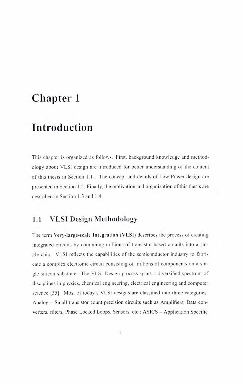
This chapter is organized as follows. First, background knowledge and method-
ology about VLSI design are introduced for better understanding of the content
of this thesis in Section 1.1 . The concept and details of Low Power design are
presented in Section 1.2. Finally, the motivation and organization of this thesis are
described in Section 1.3 and 1.4.
1.1 VLSI Design Methodology
The term Very-large-scale Integration (VLSI) describes the process of creating
integrated circuits by combining millions of transistor-based circuits into a sin-
gle chip. VLSI reflects the capabilities of the semiconductor industry to febri-
cate a complex electronic circuit consisting of millions of components on a sin-
gle silicon substrate. The VLSI Design process spans a diversified spectrum of
disciplines in physics, chemical engineering, electrical engineering and computer
science [35]. Most of today's VLSI designs are classified into three categories:
Analog — Small transistor count precision circuits such as Amplifiers, Data con-
verters. filters. Phase Locked Loops, Sensors, etc.; ASICS — Application Specific
1

CHAPTER I. INTRODUCTION 2
System-level /; design ��
/ ' 1 �� / ' 1 \ ‘ 1 I � • • 、
/ ! Funtiorial-level 'v Floorplanning - -,x - - desgin �- Power analysis
、 I , 、 ' � � ‘ T ��,, V i :(/ ' \ , � Layout : � � / ^
Simulation �� T ;、: Timing analysis ^、 、 T / /
\ 、 • '
、丨 Physical-level desgin
^ I Design checks
Post-silicon validation
Figure 1.1: VLSI Design Methodology
Integrated Circuits; Soc (System on a chip) — Highly complex mixed signal cir-
cuits (digital and analog all on the same chip). The tasks and design issues are so
diverse that a systematic approach to break the process into a number of design
layers and sub tasks is essential.
At the highest level of design - the systems level, one is concerned with an
overview of a solution, system, product, service or process. Such an overview
is important in a multi-project development to make sure that each supporting
component design will be compatible with other components. The system-level
design will include a high-level architecture diagram depicting the components,

CHAPTER I. INTRODUCTION 3
timer 1 timer 2 minutes seconds go clear
T T i T • T ~ output select
controller
timer 1 increment min timer 2 increment min
slclect increment sec slelec increment sec
unable
v 聿 v__y j timer 1 ^ buzz ^ ~ t i m e r 2 ^ display ^
——丨 r > | ——• segments
J buzzer
seconds seconds
Figure 1.2: Example of System-level Design [43]
interfaces and networks that need to be further specified or developed. The de-
sign should also depict or refer to work flows and data flows between component
systems. Figure 1.2 gives a timer chip's internal architecture at the system-design
level. Functions and interface protocols should also be defined concurrently.
The task at the functional level of design is to come up with specifications for
a conceptual solution to the problem in terms of an algorithmic process, and spec-
ifications for the major functional blocks and tlieir interconnection to implement
the major algorithmic process. If the function is too complex, it should be decom-
posed into subsystems and the process iterated hierarchically. Since the functional
decomposition induces geometrical decomposition with well-defined boundaries,
the process of design is separated into smaller subtasks that can be executed inde-
pendently. The functional level stage will hide the details of delay and timing con-
siderations by making the circuits work synchronously. In synchronous networks,
the information flow between different parts of the networks is controlled by the
clock pulses which provides time markers inside the circuit. The major design is-

CHAPTER I. INTRODUCTION 4
D c=> 1 S SET 0 I — — — 1 = > output
en ^ ^ > elk , ,
R C L R 〇
assign gclk = enable && elk; ° always @(posedge gclk)
begin • “ output=D;
end
Figure 1.3: Example of Functional Level Design
sue at the circuit-level stage are the correctness of the overall logical operations of
the circuit in terms of the elementary operations performed by the logical elements
in the specified timing sequence. At this stage, circuit schematics and some hard-
ware description languages (HDLs), such as VERILOG and VHDL, are usually
used to implement some specific functions. Figure 1.3 provides an instance of a
clock gating, which will be used to reduce power at functional level.
Interfaces between the physical world and the electrical world are the layout
layers, which serve as a linkage between the circuit design and the fabrication
process that builds the circuit. The design issue of primary concern at the layout
level is to optimize the area subject to a set of design rules to ensure that the circuit
implemented by the fabrication process will work under conservative assumptions
on process variations and the resolution of a typical lithographic step. Layout
design requires not only a knowledge of the components and rules of layout, but
also strategies for designing layouts that will fit with other circuit components to
give good electrical properties, including total wire length, area, power and so on.
At the lowest level lies the physical world of semiconductor. A complex chemi-

CHAPTER I. INTRODUCTION 5
r p ^ H ^ r 厂 I ^ II 3 . jn~n 5: L n j i 2 ' p h ^ H 1 '" l^n I “ : _ _ ~ 二 : : : ( -MS:, ⑷
— " - r r p T ^ r a 1 - ^ n - . is m b i <»5 9I J — — ; 观 : ' " " ~
叫 in — ~ i i a— ... :,::: ,<, K m '
6 ‘
1 ••••;• 二 i « ) 1 ‘
4 — ' 蜃 | 任 T 67 mmwrh51
M 丨J _ i ^ i 8 丨 劝 、
171
一 ^ ~ r-< . ' t i 7-1 ~r S - j p i 7
1, "" _ :夂 P, T 75
一 ^ 1 叫 nr—1^^¾] ―.,:: pl|;,| 111 ---/= , “ ’、!:.:」,VL-' M I 1 littll IS�6
—一」 k, 广 \ J I ; H “ ~ ' 7" 6« 4 I • ” 卜 - _ 一—f% ' j 53
I 142 r^^^^BH^^Mp*^ IM —1 ~ ' ~ IM, I I . • • • , i j
=J j—i-—— M 一L I 'i^ W|i|| J : j„ ,2 n 116 I " |「1:1 I 丨 13、 I: I irwri ___. _ .. _, - *
Figure 1.4: Example of Layout and Physical Level Design [32]
cal engineering technology has evolved to control and exploit the physical process
for the purpose of building useful devices. As these devices are put together to
form interesting circuits, the flow of currents and level of voltages become the car-
rier of in formation in the circuit. The design issues of concern at this stage are the
speed of the circuit as determined by the circuit parameters; signal degradation in
connecting wires; total power consumption of the circuit that determines the heat
buildup; and a precise sequencing of the voltage and current waveforms that con-
trol the flow of information within the circuits. Figure 1.4 shows the layout of a
floorplanning result alter power reduction from [32]. Components with different
colors work under different voltages.

CHAPTER I. INTRODUCTION 6
1.2 Low Power Design
Power and energy consumption has become one of the main design concerns in to-
day's complex digital integrated circuits. While the power dissipation of electronic
components until recently was only a small fraction of the overall electrical power
budget, this picture has changed substantially in the last few decades. Electron-
ics are becoming a sizable fraction of the power budget of a modern automobile.
These trends will only becomc more pronounced in the coming decade. If current
trends continue, energy costs, now about 10% of the average IT budget, could rise
to 50% by 2010 [24].
Reasons for the increase of power dissipation are various. Dynamic logic
circuits require some minimum clock rate in order to function properly, wasting
power even when it has nothing to do. Other circuits such as the RCA 1802 [38]
use fully static logic that has no minimum clock rate. When the clock is stopped,
such circuits use no switching power, but they still have a small static power con-
sumption caused by the leakage current. As circuit shrinks, subthreshold leak-
age [41] current is becoming much more important. This leakage current results
in power consumption even when no switching is taking place, and with modem
chips this current is frequently more than 50% of the total power used by the IC.
The first decade of power-efficient design was mostly devoted to the devel-
opment of design technologies, that is, techniques to reduce power. There are a
variety of issues to consider when developing a low-power design. Among them,
the first issue is to build accurate power consumption model. There are several
standards for modeling power. The most widely used format for modeling power
at the time is from Martin el. ai [34], It provides for pin-based and path-based
dynamic power modeling. In the former case, power is consumed whenever a par-
ticular pin on a cell undergoes transitions, whereas in the latter a flill path - from an
input transition to an output transition - must be stimulated to consume power. In

CHAPTER I. INTRODUCTION 7
— 「 \ Switching P - J Switching V current
厂- — current 厂
/ Vin—— \ Vout \ y i n — — — / V o u t
(a)
!二_」 Peak current __
^ I I Subthreshold Vin i Vout vin I ~ l e a k a g e Vout
,^-1 I 广 » r 丄 T^—l 丄
' I — i — 1 M / f __! ,r 丨 Gate leakage I 牛
I � 1 丨 i + + + + Drain junction
leakage (b) (c)
Figure 1.5: Power Consumption Models
either case, power is represented as a single value, for a particular input transition
time and output load pair, representing the total power consumed for the entire
event.
A common flow for generating power models is shown here. This flow is al-
most identical to that for generating timing models. In effect, multiple SPICE, or
SPICE-like, simulations are run on the transistor-level netlist for each cell prim-
itive: one simulation for each input transition time/output load combination for
each input-lo-output path, monitoring the current drawn from the supply. Fig-
ure 1.5 shows a transistor-level diagram of an inverter. The power model is
P = Pon+Psc^rPleak (L I )
Pon represents the dynamic power consumed when the nMOS transistor transfers
from open to close or contrarily. See 1.5(a). Pon 二 where Q is the output

CHAPTER I. INTRODUCTION 8
workload, Vod is the supply voltage and f is the clock frequency. Dynamic power
contributes about 90% of the power consumption and this ratio is decreasing. Psc
is the short-circuit power in 1.5(b) and it consume around 8% of total power. Pieuk
is the leakage power in 1.5(c) and it consume less than 2% of total power but this
ratio is increasing. A generalized low-power design flow involves both analysis
and reduction at multiple points in the development cycle. It is divided into three
phases: system-level design, RTL design, and implementations.
The system-level design phase is when most of the large design decisions are
made, especially in regards to how particular algorithms will be implemented. This
is also the phase in which designers have the largest opportunities to influence
power consumption. The primary low-power design objectives during the system
phase are the minimization of the effective switching frequency / (i.e., the product
of the clock frequency and the average switching activity) and the supply voltage
V!)D. One of the examples of a system-level low-power design technique is the use
of different operating modes in a microprocessor. If a processor is not fully active,
it should not be consuming the full power budget. Hence the clock can be slowed
down or even stopped completely. If the clock is slowed down, the supply voltage
can also be reduced as the logic needs not operate at the highest clock frequency,
a technique known as dynamic voltage scaling (DVS). Multiple levels of power-
down are possible, ranging from the limited levels to an almost continuous range of
levels possible with DVS, e.g., voltage steps as small as 20mV. However, control-
ling the power-down modes can be quite complicated involving software policies
and protocols. In addition, there is often a tracle-off between the amount of power
reduction and the time needed to emerge from a power-down mode, known as the
wake-up time. These and other trade-offs should be explored early, preferably in
the system phase and no later than the design phase, to avoid late discoveries of
critical parameters not meeting specifications. Another technique is known as dy-

CHAPTER I. INTRODUCTION 9
namic power management (DPM). DPM allows microprocessors to run in idling
mode, in which the instaiction-executing portion of a microprocessor core shuts
clown while all peripherals and interrupts remain powered and active [6].
The RTL design phase is the phase when the decisions made during the system-
level design phase are coded into executable RTL form. The implementation
phase includes both the synthesis and the physical (place and route) implemen-
tation. Clock gating is recently the most popular technique for reducing dynamic
power. See Figure 1.3 for example. It conserves power by reducing / , which in
turn reduces two different power components. The first is the power consumed in
charging the load capacitance by the clock drivers, and the second is the power
consumed by the switching of each register's internal clock buffers. Two different
flavors of clock gating are commonly used. Local clock gating involves gating in-
dividual register, or banks of registers, whereas global clock gating is used to gate
all the registers within a block of logic. Such a block can be relatively small, such
as perhaps a few hundred instances, or it can be an entire functional unit consisting
of millions of instances.
The implementation phase includes both the synthesis of the RTL description
into a netlist of logic gates and physical implementation of that netlist. It also
includes tasks such as timing and power closure and power grid verification. Mul-
tiple techniques exist for reducing power during the implementation phase, how-
ever,they are generally limited in terms of how much total power can be saved as
so most of the design is fixed by this time. Nevertheless, efforts at this level are
important in an overall low-power design flow, especially for leakage reduction.
Slack redistribution is a particularly common, and conceptually straightforward,
implementation phase power reduction technique involving the trade-off between
positive timing-slack and power [32]. As synthesizers generally work to speed
up all timing paths, not just the critical paths, many instances on the non-critical

CHAPTER I. INTRODUCTION 10
paths end up being faster what than they need to be. Slack redistribution works by
slowing down the instances of the non-critical paths, but only to the extent that the
changes do not produce new timing violations. Typical changes reduce the drives
strength or supply voltage of a particular instance [37] or increase the instance's
threshold voltage (reducing leakage power).
1.3 Literature Review on Multiple Supply Voltage
(MSV)
At the physical level, many techniques can be adopted to reduce the power con-
sumption. Adjusting transistor sizes gives rise to a continuous optimization space
and energy-delay curve. Different topologies for the same component, e.g.,an
adder, can be considered to get a set of optimal boundary curves. Among them,
multiple supply voltage (MSV) is an outstanding technique to deal with the power
problem in today's high-performance circuits. MSV design involves the partition-
ing of a chip into areas called “voltage islands" that can be operated at different
voltage levels, or be turned off when idling. With the use of voltage islands, the
chip design process is becoming more complicated. We need to solve the prob-
lems of island partitioning [18, 17, 33, 12], voltage assignment [29, 28, 31, 32]
and fioorplanning simultaneously under area, power, timing and other physical
constraints, island partitioning divides circuits into "voltage islands" where each
island occupies a contiguous physical space and operate at one supply voltage.
This kind of partition can reduce parameter variations and power dissipation. In
multiple voltage assignment, modules lying on critical paths can be operated at
higher voltage levels to satisfy timing constraints, while modules on non-critical
paths will be operated at lower voltages to reduce power consumption. Given a
net!ist of modules which can be operated at several supply voltages, the MVA

CHAPTER I. INTRODUCTION 11
problem is to assign a supply voltage to each module to minimize the total power
consumption while meeting the circuit's timing constraints. A number of previous
works were on the related problems.
1.3.1 Voltage Island Partit ioning Problems
Wu et al. [44] first researched the voltage-partitioning problem. The problem
is defined as follows. Given an m x n array A and an error threshold 5, find
a partitioning R of connected regions whose weight vv(ll) is at most 5 and the
size | n | is as small as possible. A denotes an m x grid based placement P.
Each AI/ , y'j represents the dynamic power required at the grid [i,j\. Each cell
on P will occupy some area and require its own power consumption. w ( n ) is
the total wastage in power, comprising of w(R,), where 1 < / < | n | , e U and
w(Rt) — ( m a x ( / j ) e ^ / ^ —冲,./]). They classified problems related to
the voltage island partitioning into two problems: maximally reduce power con-
sumption within given bound on number of voltage islands; and create minimally
fragmented voltage islands within given bound on power consumption. Wu et al.
designed an efficient two-step heuristic algorithm using dynamic programming to
handle both problems.
Ching et al. [12] considered a similar Voltage-partitioning problem but they
focused more on the floorplan. The regions are not restricted to be rectangular in
shape. By considering the huge size of m x n, Ching et al. built a coarsening grid
using the boundary of each cell to reduce the problem size to O(N), which is the
number of cells. After constructing the coarsening graph, Ching et cil. performed
a bottom-up clustering recursively to cluster adjacent nodes level by level. The
leave nodes on the tree denote cells and internal nodes were called "super-nodes".
Then they used a dynamic programming method to partition the tree optimally
into subtrees such that the total power wastage is minimized. The tree would be

CHAPTER I. INTRODUCTION 12
reconstructed and partitioned repeatedly until the total power wastage reached the
given threshold.
Mak et al. [33] defined the MSV problem as follows. Given a netlist of cores,
a fioorplan of the cores, the legal voltage levels of each core and the corresponding
power consumptions at different voltage levels, determine a proper voltage level
for each core. Mak et al formulated the problem as an integer linear program
(ILP) by taking both the voltage assignment and island generation problems into
account. The objective function is
cost 二 Prulai + p . F
where P ! o t a j denotes total power consumption, comprising of the power consump-
tions PCores of all the cores, and the power consumptions Pshifters of the level
shifters. Level shifters are used to help cores at low voltage level to drive cores at
high level. The parameter P is an user specified parameter. F is defined to be equal
to the number of pairs of physically adjacent cores operating at different voltage
levels and is used to measure the fragmentation of the power network. Since there
were no timing constraints, they assumed an upper bound on the desired power
consumption Pbound- Then they tackle this problem by solving the ILP problem.
1.3.2 Multiple Voltage Assignment (MVA) Problem
In [28], Lee et al. solved the MVA problem by dynamic programming. At the
same time, they presented a power network aware floorplanner to generate floor-
plans with voltage islands after the voltage assignment. As we will compare with
this paper in chapter 3,we will explain this paper in more details as follows: The
problem is formulated as: Given supply voltage and delay pairs, a set of cells, a
netlist and a fixed static-timing constraints, assign a supply voltage and coordinate
to each eel! in a flooiplan so that the total power consumption and power-network

CHAPTER I. INTRODUCTION 13
resource requirement are minimized and all constraints are satisfied. Lee et aL
first provide a dynamic programming (DP) based method to solve this voltage as-
signment problem. After supply voltages are assigned to circuit cells, level shifters
are inserted into the circuits, which arc used to transmit current from cells at low
voltage level to higher one. Finally, they transformed the precomputed slack into
the wire length constraint and perform floorplanning on all blocks, including cir-
cuit blocks and level shifters, to minimize the power-network resource require-
ment. The floorplanning is based on simulated annealing (SA) using the 召*-tree
floorplan representation.
In [31], Ma et al. considered the problem of island partitioning and voltage as-
signment, except for the timing constraints. First, simulated annealing was adopted
to perform the random search to generate a candidate floorplan in each step, then
they used DP with an efficient cost table update technique to compute the smallest
possible power consumption for each candidate floorplan solution. In the floor-
planning step, they also generated islands with power down mode to optimize the
total power consumption further. The problem in [31] is formulated as: Given a
set of cells with aspect ratio bounds, a power table that specifies the legal voltage
levels for each cell, a set of net and a set of groupings between the cells such that
cells in each group have similar inactive periods and will save power consumption
if they are grouped together on one island, generate a fioorplan with minimum to-
tal power consumption. Ma et al could solve the island partitioning and voltage
assignment problem optimally for slicing floorplans. Given a candidate floorplan
solution represented by a normalized Polish expression, they constructed the cor-
respondijig slicing tree and partitioned the subtree under the root into several sub-
trees to minimize the total power consumption such that the cells represented by
leaves in each of the subtree will form one island operated at one common voltage
possibly with power down mode while the remaining cells not belonging to any of

CHAPTER I. INTRODUCTION 14
the subtrees will be assigned to the highest deep-level voltage.
Ma el al. considered this problem further in the paper [32] by taking timing
constraints into account. They still used the same floorplanning framework, but
showed that the voltage problem under timing constraints for each candidate floor-
plan solution could be solved optimally on the condition that the delay choices
(each delay choice corresponds to a choice of the working voltage level) are con-
tinuous in the real or integer domain. This problem can be transformed to a convex
cost network flow problem. After applying the Lagrangian relaxation technique,
the problem can be solved optimally by a cost-scaling algorithm in polynomial
time. In this problem, a delay-power curve (DP Curve) is given instead of the
supply voltage table and a timing requirement Tcycie, called clock cycle time, is
considered. Ma el al. first represented a circuit by a directed acyclic graph (DAG)
by transforming each cell to a vertice and each wire to a directed edge (forming
a set of edges callcd E\) and split each vertex (circuit cell) into two vertices and
linked them up by several directed edges (forming a set of edges called Ei) with
several choices of delays. Then, the original problem was formulated into a math-
ematical program:
Minimize !^/,供成⑷)
Subject to
tj - t, > dir, eE (lb)
o<tt< Tcycle, viev (lc)
!ij ye(ij)eE (lei)
…, }々, (1七)
而 GZ十, y e ( i j ) e E 2 (1 / )
ti e z + V/ G v (1 尺)
since each vertex (circuit cell) is split into two vertices, the the delay dv of cell v

CHAPTER I. INTRODUCTION 15
will be represented as <:/", where i j are new vertices generated by v. Pjj(ciij) is the
power consumption of each pair (/',/). /; is the arrival time for each vertex, is the
delay of each edge. Ma et al. used the Tcvc/e to represent the clock cycle and cl)'丨1 to
denote the delay of a cell working under the voltage level k". This problem can be
transfonned to a convex cost network flow problem and solved optimally [4]. After
Ma et al. obtained the solution, they in turn calculated the objective function of
the simulated annealing algorithm and generated new candidates until the solution
was good enough.
1.4 Literature Review on Dynamic Voltage Scaling
and Dynamic Power Management
In system-level designs, there exist many methods to reduce power dissipation.
For example, the specific architectures and algorithms can be further explored,
functions can be mapped to software and hardware blocks for power efficiency.
One should also evaluate power consumption for different operational modes and
generate budgets. Among them, two well known techniques that can be used for
energy minimization are: dynamic power management (DPM) [6] and dynamic
voltage scaling (DVS) [42, 21]. These system-level energy management tech-
niques achieve energy reduction by selectively switching off unused components
(DPM) or by scaling down the performance of individual components in accor-
dance to temporal performance requirements of the application (DVS). Figure 1.6
shows a block diagram of a typical DVS-enable and DPM-enable processor [8]. A
microprocessor core carries out the required computations. This processing unit
is connected through a system bus to the static memory (cache unit) and the I/O
bus interface. The heart of this system, which enables a dynamic voltage selection,
consists of a DC/DC voltage converter, a specialized frequency register and a volt-

CHAPTER I. INTRODUCTION 16
SBus
^ \ R e g .
f d Microprocessor Core ^ • 5 Q
§ g ^ ^ ——t fc
Q ^ i , t ^ , fc — r — O Q j j T Vdd
I/O SRAM
Figure 1.6: A Typical Chip Design with DVS and DPM
age controlled oscillator. Supply voltage and operational frequency are changed
by writing the desired frequency j j into the frequency register. Upon writing the
desired frequency into the register, the DC/DC converter compares this frequency
with the current frequency fc and either increases or decreases the supply voltage
VJJ. Various chip makers have recently introduced processors with DVS capabil-
ity [1, 3, 2]. A number of strategies are provided to guide the designers in previous
works.
1.4.1 Dynamic Voltage Scaling (DVS) Problem
DVS problems have been explored by a lot of works. At first, time-interval based
methods are provided to run tasks on time [42, 9, 40, 16, 25]. Weiser et al. [42]
proposed to divide the time axis into segments with the same length and fixed
the speed of processors to complete most of the tasks before the deadline. They
analyzed the usage of processor in the previous time segment. If the usage exceeds

CHAPTER I. INTRODUCTION 17
a defined threshold, the processor starts to speed up; otherwise, it reduces its speed.
Weiser et al. also allows latency and will first run tasks left by the last segments.
Chung et al. [9] implemented several strategies in a computer and proposed four
different methods.
» AVR: This method uses both the usage of the processor in the last time
segment and the historically accumulated usage to estimate the workload in
the current time segment. They introduce a weight to denote the effect of the
accumulated usage, old and new represent the accumulated usage and the
usage of the previous time segment respectively. The current speed is set as
speed 二 [weight x old + new) /{weight + 1)
• Long—short: This strategy uses both the average usage in the last three time
intervals and the average usage in the last 12 time intervals. These two
factors have different weights and together determine the current speed.
• Cycle: It tries to find the periods of tasks. The previous 16 time intervals
will be checked for the existence of any period. If not, the process will use
a constant speed; otherwise, it will follow the periodical variations.
m Peak: The strategy pays more attention to the peak of the usage, compared
with other strategies above. If the usage of the processor is decreasing, the
strategy will predict that the usage will continue decreasing. If the usage is
very high, the strategy will guess that the usage will climb up to the peak
and decrease soon. Of course if the usage is low and smooth, it will have a
large chance to keep the safe.
Chung et al. concluded that complicated strategies for estimation will not perform
better than relatively simple and smooth strategies that keep the process running
stably. Pering et al. [40] and Grunwald et al. [16] provided the concept of task-
based DVS strategy. They suggested that if tasks could be completed before its

CHAPTER 1. fNTRODUCllON 18
deadline, the performance of the processor was then acceptable. A new strategy
called Pace was proposed to tackle the new problem. Pace assumes that the speed
of the processor is continuous. First, it classifies the usage of the processor into
different levels. Then they set the corresponding speed for each level. In the
paper [15], Yao et al. investigated the online AVG algorithm which allocated tasks
evenly between its arrival time and deadline. They also gave a competitive ratio
(CR) between their algorithm and the optimal solution. The problem is formulated
as follows. An instance of the scheduling problem is a set J of jobs to be executed
during 丁 二 [/(),/�].Associated with each job j e J are the following parameters:
• a j is y's arrival time,
• b j is / \s deadline (b j > a丨),and
• R j is its required number of CPU cycles.
A schedule is a pair S 二 (s, job) of functions defined over T:
• s ( f ) > 0
• job(t) defines the job being executed at time /.
A feasible schedule for an instance J is a schedule S that satisfies
广、(/)5(—(/),加二& Jaj
for all j G J, where 8(x;>') is 1 '\ix~y and 0 otherwise. The total energy consumed
by a schedule S is
E{S) = I'' P(s{/))cit. 人()
The goal of the scheduling problem is to find a feasible schedule that minimizes 、 . R.
E(s). Yao el al. defined the average-rate of each job j as clj — and provided
both an offline optimal algorithm and an online algorithm called Average Rate

CHAPTER I. INTRODUCTION 1 9
Heuristic (AVR). In the offline algorithm, Yao et al. defined the intensity of an
interval / = [z,z'] to be
g � = -r' "7
where the sum is taken over all jobs j with [aj, bj] < [z,z'}. Then they repeated the
following steps until J is empty:
• Identify a critical interval /* : [z,z'] by computing s : max g(I), and
schedule the jobs i n a t speed over the interval r by the earliest deadline
policy.
• Modify the problem to reflect the deletion of jobs J ” in the interval I*.
In the online algorithm, at any time t, set the processor run at speed s(t) 二 lLjdj{t).
In [15], they analyzed the competitive ratio CR — AVR(J)/OPT(J) and obtained
pp < CR < 2P"1 pp. But Yao et al. assumed that the expression for power con-
sumption is P(s) = sp, where s is the speed of the processor, and there is neither
power consumption nor wake-up time for the idling state. As a result it is benefi-
cial to execute a task as slow as possible.
Bansai et al. [5] analyzed another online algorithm based on the same model.
Their proposed algorithm computes the optimal available schedule based on the
jobs currently known. At any time /, their algorithm adopted Yao et al. 's offline
algorithm according to the known jobs and executed jobs until completion or until
new jobs' coming. The competitive ratio is formed to be 2{-^)pep, where e 二
2.718.
Irani et al. [20] considered a more general expression for the power consump-
tion function and took both the idling mode and sleep mode into account. Based
on the assumed power consumption function, they computed an optimal speed to
minimize power usage when the processor was active. They assumed that no en-
ergy would be consumed during sleep mode except that one unit of extra energy

CHAPTER I. INTRODUCTION 20
was required for the processor to wake up from sleep mode. They designed both
an offline and an online algorithm to tackle the problem, that is formulated as fol-
lows. A schedule S consists of a triplet S — (,s\ job) where ¢(/) is defined over
[/()• /1] and indicates which state the system is in (sleep or on) as a function of /.
Other parameters are the same as those in [15]. Then
/
P(s) i f (|) 二on { (1-2)
0 i f c|) = s l e e p
V
Let k be the number of times that a schedule S transitions from the sleep state to
the on state. The total energy consumed by is
二/(+ 广 P(s(j)M0)出
They computed the critical speed sa.-u to minimize J where 穴 is a constant.
The offline algorithm is derived from Yao et. al. 's offline algorithm. The difference
occurs when the average speed g(J*) < scrn and the processor will run at the critical
speed in that case. The processor will prefer to stay at the previous state. That is,
if u is idling before the execution of jobs in the next interval, it will postpone
the starting time of executing the jobs as late as possible while it still can finish
all the jobs before their deadlines. If it is on, it will keep executing jobs until
there is no new job. Their online algorithm obeys the same rule. The competitive
ratio (CR) of their offline algorithm is two and the CR of their online algorithm is
max{cic2 + c\ + 2 ,4} where C\,C2 are constants.
1.4.2 Dynamic Power Management
Unlike DVS, dynamic power management (DPM) is already around for quite a
while. The main strategy of DPM is the shutdown of idling system components [7,
30]. DPM approaches often differ in the employed shutdown policies (or power

CHAPTER I. INTRODUCTION 21
management policies). For example, in its most aggressive strategy, components
are switched off immediately when they become idle. A second strategy is the
timeout-based policy, that switches off components after a fixed idling interval.
This policy is well known from the advanced power management widely used
in today's notebook computers. Nevertheless, since the restart of a component
involves a time and power overhead to restore its fully functional state, such greedy
policies might not result in power savings or may even increase the dissipated
power. Therefore, a careful application of the prediction is necessary to achieve
the highest possible power savings. The quality of a power management policy
depends therefore on the accuracy with which the future behavior of the system
can be predicted, in order to start-up currently inactive components or to shut down
currently active components at the right moment.
For the two-state problem, e.g., active and sleep state, an online algorithm
consists of a single time threshold T after which the algorithm will transit from the
on to the sleep state. The best deterministic online algorithm will stay in the high
power state until the total energy spent is equal to the cost to power up from the low
power state, [t is known that this algorithm achieves the optimal (deterministic)
competitive ratio of two [23]. When one considers randomized online algorithms,
the best competitive ratio achievable is improved to [23]. If the idling period
is generated by a known probability distribution, then the algorithm that chooses
threshold T so as to minimize the cxpected cost is always within a factor of of
optimal.
[n paper [19], Irani et al. examined the multiple-state problem from the per-
spective of worst-case guarantees. They considered the special case where the
cost to power-down is zero and the algorithm only pays to move from low power
states to higher power states. The paper [19] gives natural generalizations of the
algorithms for the two-state case both for the case when the idling period length is

CHAPTER I. INTRODUCTION 22
unknown and when it is generated by a known probability distribution. It is shown
that when the transition costs are additive, e.g., the power consumption required
foi. transition from sleep state one to three is equal to the sum of power consump-
tions for transitions from sleep state one to two and two to three, the general-
ized deterministic algorithm is 2-competitive and the probability-based algorithm
is -competitive.
1.5 Thesis Contribution and Organization
In this thesis, we study the low power design at physical and system level, focus-
ing on the Multiple Voltage Supplies (VIVS) (in section 1.3), the Dynamic Voltage
Scaling (DVS) and the Dynamic Power Management (DPM) techniques (in sec-
tion 1.4), and propose some approaches to address two low power design problems.
In Chapter 2, we study the static voltage assignment problem at the physical
design level. At this level, the multiple voltage assignment (MVA) problem under
timing constraints in floorplanning, which is generally an NP-hard problem, is
very important. Ma et. al. solved the problem in [32] optimally by assuming
that the delays at different voltage levels of a cell is are continuous in the integer
domain. They did not take level shifters into account. In our work, we allow the
delays to be discrete arid consider the power consumption of level shifters. We
present an effective value-oriented branch-and-bound based algorithm to solve the
problem optimally in a reasonable amount of time. A convex cost integer dual
network flow approach is used to obtain a feasible upper bound solution, while
a lower bound is obtained by a linear relaxation of a general formulation of the
problem. We then adopt a value-oriented breadth-first branch-and-bound method
with the upper and lower bounds obtained as described above to search for the
optimal solution. Then we embed this algorithm into a multi-stage floorplanner.
Experimental results show that we can improve over the latest previous work on

CHAPTER I. INTRODUCTION 23
this problem [32] by further reducing 6% of power consumption while maintaining
the performance on other factors.
In Chapter 3, we propose a general scheduling method to capture the key char-
acteristics of both dynamic voltage scaling and dynamic power management. In
our model, a processor in active mode can run at a number of speeds and each
has a di fferent energy consumption rate. The processor can also sleep in a number
of sleep modes and each has a different wakc-up latency and energy consumption
rate. We found that (he offline version of that dynamic voltage scaling problem can
be formulated as a quadratic program, and can be solved optimally in a reasonable
amount of time. We will also present an effective algorithm to solve this problem
online that can achieve good competitive ratios in tenns of power consumption in
comparison with the optimal offline results. We calculated several critical speeds
by considering di fferent sleep modes and make the processor execute jobs mainly
at these specific speeds. This method can achieve advantages in terms of both
power consumption and latency. The experimental results show that our approach
out-performs most of the state-of-the-art techniques in power consumption and
latency.
Finally, we give the conclusions of this thesis in Chapter 4.
• End of chapter.

Chapter 2
Multi-Voltage Floorplan Design
2.1 Introduction
Multiple Supply Voltages (MSV) is developed to deal with the power problem
in today's high performance circuits. In MSV designs, modules lying on critical
paths can be operated at higher voltage levels to meet timing constraints, while
modules on noncritical paths will be operated at lower voltages to reduce power
consumption without affecting the circuit performance. However, a number of is-
sues must be handled first before this approach becomes practical, for example,
voltage selection and assignment. MSV-avvare fioorplanning and placement, etc.
Among them, Multiple Voltage Assignment (MVA) is an important problem that
has attracted the attention of many researchers in the past few years. Given a netlist
of modules which can be operated at several different supply voltages, the MVA
problem is to assign a supply voltage to each module to minimize the total power
consumption while satisfying the circuit's timing constraints. In MSV designs,
the timing slacks of the modules are traded for power saving under a performance
guarantee of the circuit. Therefore, an efficient voltage assignment method is de-
sirable to minimize power consumption under timing constraints. Besides, it is ab-
2 4

CHAPTER 2. MULTI- VOLTAGE FLOORPLAN DESIGN 25
solutely beneficial to consider this multi-voltage design issue at the floorplanning
level so that those important physical information like interconnect delay, module
location (for estimating the power network routing resources) and area overhead
due to level shifters, etc. can be taken into account in an early stage.
A number of previous works were on these MSV related problems. MSV was
considered at various design stages, including the floorplanning and placement
stage 丨 17, 31], and the post-floorplanning and post-placement stage [27, 33, 45].
f n � 2 8 ] , Lee et al. used a dynamic programming based algorithm to solve the
voltage assignment problem. In [32], Ma et al, transformed this power assign-
ment problem to a convex cost integer dual network flow problem [4j which can be
solved in polynomial time. However, none of them can produce optimal solution
for the problem in general. Lee et al. [27] formulated the problem as a mixed inte-
ger linear program (MILP), and used a general linear programming solver to obtain
optimal solution but the runtime can be excessively long. Chang and Pedram [11]
proved that the MVA problem was an NP-harci problem, even if each module had
only two voltage choices (the two choices could be different for different modules
though).
In this chapter, we will first develop a technique that can solve the general volt-
age assignment problem under timing constraint optimally in a reasonable amount
of time, assuming that the delay-power curve for each module is convex [13].
Given a floorplanning result containing a netlist of modules, a number of working
voltage levels for each module with the corresponding delays (delay choices can
be continuous or discrete in the real or integral domain), interconnect delays and
a timing constraint T, a voltage level will be assigned to each module such that
the maximum power saving is achieved without violating the timing constraint.
Secondly, we develop a floorplanning strategy with this optimal voltage assign-
ment technique that can perform better on power saving than the most updated

CHAPTER 2. MULTI- VOLTAGE FLOORPLAN DESIGN 26
work [32] on the MSV-driven floorplanning problem while maintaining the per-
formance on other factors.
In section 2, we present a general formulation of this voltage assignment prob-
lem. In section 3, we show how to solve this problem optimally by using a value-
oriented branch-and-bound based algorithm. In section 4, we integrate this optimal
voltage assignment with floorplanning. fn section 5, we show the experimental re-
sults.
2.2 Problem Formulation
We are given a set of/7 modules m\, mi,..., mn with areas and aspect ratios. Each
module m\ is given kL choices of supply voltage vcj, for 1 < ^ < Iq, and the corre-
sponding delays cf!. We are also given the delay and power for one level shifter that
must be inserted in a signal line connecting a low voltage cell to a high voltage cell
and a timing requirement Tcvc/c. (This is called the clock cycle time and is an upper
bound for all critical path delays.) In the following, we define the multi-voltage
floorp 1 ann ing prob 1 em.
Definition 2.2.1 Multi-voltage Floorplanning - Given a netlist of modules, each
of which has multiple choices of supply voltages and corresponding delays, and a
clock cycle, generate afloorplan with a voltage assignment to each module such
that the timing constraint is satisfied and a weighted sum of the total power con-
sumption (due to cells and level shifters), power network routing resources, area
and wire length is minimized.
The power-delay trade-off in m-, is represented by a delay-power curve (DP
Curve), { ( c J j , . . . ( d k / , p { ) } , where each pair (dj.pj) for q = 1 , 2 , . . .,、
is the corresponding delay and power consumption when is operated at vcj.
Note that each dcj and pLj can be any real or integer number as long as the DP-
CHAPTER 2. MULTI- VOLTAGE FLOORPLAN DESIGN 27
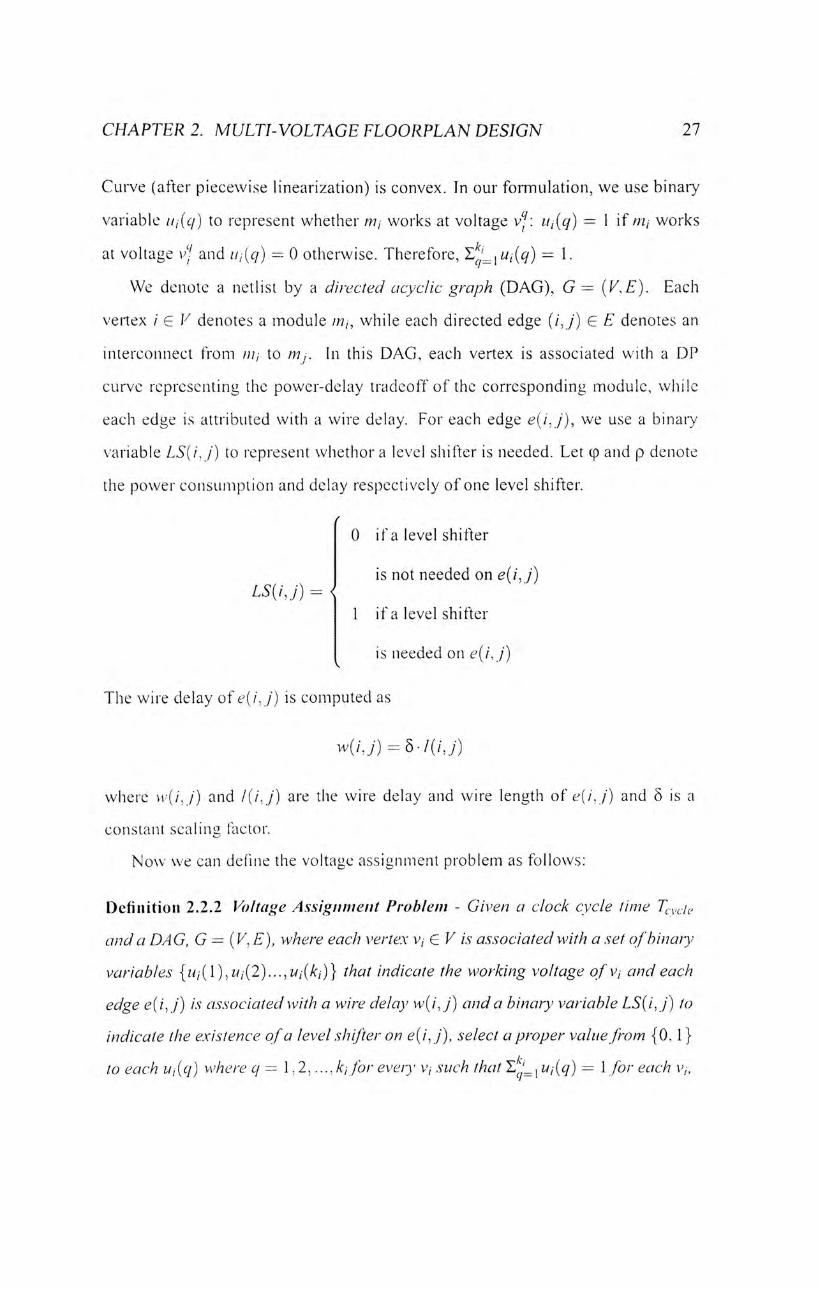
Curve (after piecewise linearization) is convex. In our formulation, we use binary
variable i/,(c/) to represent whether w/ works at voltage v^: u^q) 二 1 i f w o r k s
at voltage vj and iij{q) 二 0 otherwise. T h e r e f o r e , 《 '二丨⑷ 二 1.
We denote a netlist by a directed acyclic graph (DAG), G — Each
vertex i G V denotes a module m“ while each directed edge (/, y) G E denotes an
interconnect from nv, to m,. In this DAG, each vertex is associated with a DP
curve representing the power-delay tradeoff of the corresponding module, while
each edge is attributed with a wire delay. For each edge ¢(/, /) , we use a binary
variable LS{i, j ) to represent whethor a level shifter is needed. Let (p and p denote
the power consumption and delay respectively of one level shifter.
(
0 if a level shifter
is not needed on e(i, j) LS(ij')= <
1 if a level shifter
is needed on <?(/, /)
The wire delay of e(/, /') is computed as
w(/,_y.) 二 5 . / ( / ,y )
where vi'(/,/.) and /(/', / ) are the wire delay and wire length of ^( / , / ) and 5 is a
constant scaling�actor.
Now we can define the voltage assignment problem as follows:
Definition 2.2.2 Voltage Assignment Problem - Given a clock cycle time Tcycie
and a DAG, G 二 ([E),where each vertex v/ G V is associated with a set of binary
variables {"/(1), w/(2)..•,"/(/:/)} that indicate the working voltage of v/ and each
edge e{i�j) is associated with a wire delay w{ij) and a binary variable LS(i, j) to
indicate the existence of a level shifter on e(ij), select a proper value from {0. 1}
to each Uj(q) where q — 1; 2,...: k, for every v,- such that Z � = 1 Uj{q) — 1 for each vh

CHAPTER 2. MULTI- VOLTAGE FLOORPLAN DESIGN 28
'〈 - /; :…-- ®—--、 -、 : :、、
(a) (b)
Figure 2.1: DAG Transformation
the total power consumption due to the cells and level shifters are minimized and
the timing constrianl is satisfied.
For formulation simplicity, we will transform G 二 (V,E) into a new graph G =
[V,E) by adding a virtual module m() as well as a set of virtual edges Eq. Hence
V — V U {mo} and E — ED Eq. The set Eq contains (i) edges ^(0, z) for all m-,
which have no incoming edges in G and, (ii) edges e(i,0) for all w/ which have no
outgoing edges in G. An example is shown in Figure 2.1 in which sub-figure (a)
is the DAG G and sub-figure (b) is the corresponding G. We will put IIQ(CJ) = 0 Mq
and put h,(/ . /) = 0 and LS(iJ) 二 0 \/e(i,j) e E(�.
According to the definition and notation above, the voltage assignment prob-
lem can be easily formulated into the following mathematical program.
Minimize : lVjeVi:l^]pqliii(cj) -f Leii J)eELS(i, j) • (p (2.1a)
Subject to :
'二…⑷二 1 V ^ e 厂 (2.1b)
工J㈣(^;二一卜咖)+ PLS(I,J) + WQ,乃)< TCYCLE
Vc G (2.1c)
f 0 t ' ^ x u ^ y ^ ^ x u j i q ) LS(l,J)= Q Q J ( 2 . I d )
1 otherwise 、
iiiiq) G {0,1}, q = 1 , 2,…,々 ,,•、々 G V (2.1e)

CHAPTER 2. MULTI- VOLTAGE FLOORPLAN DESIGN 29
/ \ w
'(1) = 0 ;
/ \ "丨 ( 2 ) = 1 •
d) ....(¾ �=i i,t(\) = \ V ° v V J
«,(2) = 0 h,(2) = 0 : •• "丨⑴=丨"、⑴=0 t/,(A-,) = 0 / ,(/:,) = 0 m,(2) = 0 (2) = ()
"丨(々丨)=(> (。(々 ,)=I
Figure 2.2: Sample of Branch-ancl-Bouod Method
where is the set of all cycles in G, The objective function (2.1a) is the sum of all
modules' and level shifters' power. Constraint (2.1b) is used to ensure that each
module //?/ is working at only one voltage level. Constraint (2.1c) is the timing
constraint that requires the delay of every path to be smaller than the clock cycle.
2.3 A Value-Oriented
Branch-and-Bound Algorithm
In this section, we will show how to solve the MVA problem optimally. As we
mentioned before, the MVA problem is an NP-hard problem, so we developed
a branch-and-bound based technique to solve it. We will first dcscnbc the basic
value-oriented branch-and-bound algorithm and then explain how to compute the
upper and lower bounds. The branch-and-bound approach solves problems by
searching successive partitions of the solution space. As usual, we will describe
the searching process by a search tree in which an internal node represent a set of
solutions while a leaf node represent a single solution.

CHAPTER 2. MULTI- VOLTAGE FLOORPLAN DESIGN 30
2.3.1 Branching Rules
In our searching approach, we visit different parts of the solution space by con-
fining the value of some selected variables. An example is shown in Figure 2.2.
Node zero represents the set of all solutions (an optimal one exists for the original
problem). In the first iteration, we may select a module nij (we will describe the se-
lection criteria in the following) and branch to k\ children nodes, which represent
the solution space of k, different subproblems where kt is the number of supply
voltage choices of module m,-. W.l.o.g., we assume that this //2/ is m\ in the follow-
ing discussion. In figure 2, S\ is the first such subproblem which is obtained by
adding the following constraint (2.2) to constraints (2.1 a)-(2.1e):
ui � 二 l,in(2) ( ^…,…⑷)二 0 (2.2)
Similarly, subproblem is obtained by adding to constraints (2.1a)-(2.1e),(2.2)
and a new constraint (2.3):
"3(1) 二 1,"3(2) 二 0,...,"刺=0 (2.3)
In this way, we will branch out to many subproblems and search the whole solution
space of the original problem. Next, we will discuss selection criteria for braching
cut. In [32], the author presented an algorithm that can give an optimal solution for
the MVA problem when the voltage choices are continuous. But this may not be
true in many real applications. For example, in a problem with two supply voltage
choices for each module, e.g., module ;;?/ has two choices [p],cl]) and the
approach in [32] may return a delay value cf;ptllllul for nij where d) < d?1111101 < d]
(assuming d) < d}). Notice that f l n i a l is equal to d) or d^ exactly, we say that
the solution is feasible; otherwise, it is infeasible. Therefore, to branch out from
a node, we will select the module with the lowest index whose solution returned
by [32] is infeasible. For instance, given a MVA problem, we first solve it using the
approach in [32] and obtain a solution for module

CHAPTER 2. MULTI- VOLTAGE FLOORPLAN DESIGN 31
m\,m2, we will check starting from i 二 1 to /c whether module w, can work at
(p*,cl*), and select the first module whose solution is in feasible to branch out to the
children nodes. After selecting one module m“ we will construct kt subproblems
with additional constraints to confine the voltage level of w/ where Jq is the number
of voltage choices for "?/.
2.3.2 Upper Bounds
For a bra11c 11-and-bound based algorithm, tight upper and lower bounds are im-
portant for efficiency. As we mentioned above, the approach in [32] may produce
infeasiblc solution, bccause the convcx cost integer dual network flow algorithm
may return voltage values lying between two feasible voltage levels.
Table 2.1: Number of Cells With Infeasible Voltage Levels
nlO n30 : n50 nlOO n200 n300
No. of cells with
infeasible voltage 3 6 9 5 21 � 3
We have collected some statistics (Table 2.1) that shows the number of in-
feasible assignments voltages returned by the approach in [32]. Since the num-
ber of infeasible voltages is relatively small, one good and straight forward way
to obtain an upper bound for the searching process is to choose a feasible so-
lution as close as possible to the solution returned by [32]. Given a solution
{(;;*, d\), (p* ,《),...{d* for modules m \. mj,. ..mn, n is the number of mod-
ules, if some (p'j, d*) for 1 < / < n is not feasible, we can use the largest possible
dj in (Pi-.^j) such that

CHAPTER 2. MULTI- VOLTAGE FLOORPLAN DESIGN 32
and satisfying d i < d* as the voltage level for m”
After assigning supply voltages to all modules, we will check for each net (/’_/),
whether a level shifter should be inserted. We will then use the sum of the power
consumptions due to the modules and the level shifters as an upper bound. Note
that we vvili do this computation whenever a new node in the search tree is visited
and will update the upper bound (which is global) if a better one is found.
2.3.3 Lower Bounds
The lower bound is obtained by a linear relaxation of the problem. Before we
explain it, let us rebuild the formulation of Problem (1). Let k be the total number
of supply voltages among all the modules. For example, if we have three modules
ni\, mi and /773 where m\ has only one supply voltage choice /?J = 1 .Ov, 1112 has two,
p\ — 1 .Ov and p�—1.2v,and "73 has two, p\ = 1.1 v and p\ 二 1.4v, then we will
have /c 二 4 different voltage levels I .Ov, 1.1 v, 1.2v, 1 Av for all the modules. Now,
we will substitute each kj in Problem (1) by /r and replace iij{q) for q 二 1,2,...,A'/
by u,{q) for q : 1,2,.. . , A:. For the above example, before this step, module /773
will have k�— 2 voltage choices, and after this step, k = 4 but z/3(1) and 1/3(3) are
always zero because they represent 1 .Ov and 1,2v respectively and /773 cannot work
at these two voltages.
In the linear relaxation, we first replace (2.1e) by
0 < iii(q) < 1 , 2 , . . . , � V V / . G 厂
Then we can substitute (2.Id) by
L S { i j ) > Hi(qi) + uj{q2) — 1
Ve(/,y) e£’W/r•豹 s.t. { 0 < q x , q 2 < k ) A { q 2 > q \ ) (2.4)

CHAPTER 2. MULTI- VOLTAGE FLOORPLAN DESIGN 33
So Problem (1) becomes the following after this linear relaxation step:
Minimize : l ^ y ^ ^ p j + H(iij)eELS(i,j). cp (2.5a)
Subject to :
l / ^ u A q ) 二 1 V v ^ K (2.5b)
+ + < Tcycle
V c € (2.5c)
LS(i. j ) > « ) + u八c/2) — 1
M'J') € Eyq^cn s.t. (0 < q\,q2 < k) A (c]2 > q{) (2.5d)
{)<LS(i.j)<\^e{ij)eE (2.5e)
0 < ii;{q) < 1,? 二 V (2.50
Note that the optimal solution to Problem (I) is included in the solution space of
Problem (5), so the power consumption of the optimal solution of (5) is a lower
bound for our Problem (1). Problem (5) is a simple linear program which can be
solved easily with the simplex algorithm in polynomial time to give a lower bound
to our original problem.
2.3.4 Pruning Rules and Value-Oriented Searching Rules
With the upper and lower bounds obtained above, we can construct our pruning
rules. Some nodes with their subtrees together will never contribute an optimal
solution, and good pruning rules help to find such nodes to reduce runtime. If a
node is infeasible, that is, we cannot find a feasible solution satisfying the timing
constraint even assuming a continuous domain for the module voltages (this can be
verified by invoking the approach in [32]), it will be pruned. Besides, if a node's
lower bound is greater than or equal to the global upper bound, it will also be
pruned. This is correct since we can never find a better solution by traversing into

CHAPTER 2. MULTI- VOLTAGE FLOORPLAN DESIGN 34
its subtree.
With the above bounds and pruning rules,we can search the solution space
taster. Our value-oriented branch-and-bound searching algorithm is divided into
rounds. In each round, we set a target which is used as a threshold to decide
whether a node should be visited in this round. For example, in the first round, the
target will be computed as:
target 二 a�Oupbounci + Oiowbounc/)
where 0 < a < 1 is a constant (set to 0.6 in our experiments), and O u p — and
O low bound are the upper and lower bounds of the original problem (node 0 in Fig-
ure 2.2). When we reach a node S, we will check whether S—nd < target where
Sjowbound is the lower bound at S. If so, we will continue to visit the subtree of S;
otherwise, this node S will be marked and will not be visited in this round (may
be visited in the following rounds). After one round, the value of target will be
updated as target — target -f- C where C is a constant (set to 5% of Oup/)0linc/ in our
experiments). Note that a subtree which is explored in a previous round will not be
repeatedly visited in any subsequent rounds. In general, this value-oriented search-
ing strategy will search nodes with smaller lower bounds in earlier rounds and we
can upper bound the deviation of a solution obtained from such value-oriented
search from the true optimal solution. This idea is derived from the target-oriented
branch-and-bound algorithm in [39],
In our value-oriented branch-and-bound algorithm, There are two conditions
under which we can stop searching: (i) a feasible solution is found at a node of
which the objective function value is equal to the smallest lower bound (obtained
by the linear relaxation) ever seen during the search; (ii) all possible nodes are
visited and searched.
Putting all the above steps together, we have the following pseudo-code for our
vaiue-oriented brand-ancl-bound algorithm:

CHAPTER 2. MULTI- VOLTAGE FLOORPLAN DESIGN 35
Algor i thm 1 Value-Oriented Branch-and-Bound i: II Procedure to find optimal solution to the voltage assignment problem
2: PMVA //solution to the multiple voltage assignment problem assuming contin-
uous domain for voltage choices
3: pool = 0 //' a queue for searching nodes
4: basket — 0 // a stack for searching nodes
5: nodEO 二 construct first node from PMVA
6: put node�into pool
7: while (pool is not empty) do
8: node�— get a node from pool
9: p u s h nodex i n t o basket
10: while {basket is not empty) do
11 : nodex — Pop node out of basket
12: if (nodex can be cut) then
13: goto line 10
14: end if
15: if {nodex can be stored in the pool for subsequent iterations) then
16: store nodex in pool
17: goto line 1 0
18: end if
19: branch at nodex
20: push all subproblems into basket
21 : end while
22: end while
2.4 Fioorplanning
We integrated the above optimal voltage assignment algorithm into the fioorplan-
ning step. Our floorplanner is multi-stage. In the first stage, we will invoke the

CHAPTER 2. MULTI- VOLTAGE FLOORPLAN DESIGN 36
simulated annealing based floorplanner in [31] to give an initial floorplan. After
an initial floorplan is generated, we will perform our optimal voltage assignment
on it. Finally, a post-processing step will be performed to incrementally change
the floorplan to reduce the network routing resources before a final optimal voltage
assignment is performed once again. The post-processing step is done by invok-
ing an ordinary simulated annealing based floorplanner which will move blocks
around to minimize an objective function which is a weighted sum of area, wire
length and power network routing resources (no power consumption in the cost
function). After this fast floorplanning step, the timing constraint may be vio-
lated, so we need to perform once again the optimal voltage assignment to assign
a final voltage to each block. The floorplanner [32] is used to produce the initial
floorplan because their approach is very similar in nature with our optimal volt-
age assignment method and the second stage thus will not make a large number of
block voltage changes, which, basically, will invalidate and waste the optimization
done in the first stage. To verify this point, we have done a simple experiment
to compare the results of the minimum cost network flow approach used in [32]
and our optimal voltage assignment method. We randomly generate 10 floorplans
for each benchmark and compare our approach (called VOBB) and [32] in terms
of average power consumption ancl the number of modules with different voltage
assignments. The results are shown in Table 2.2.
2.5 Experimental Results
We implemented our algorithms in the C programming language and experimented
on a PC with an Intel 2.6GHz CPU and 1 GB memory. We have done two sets of
experiments as described below.

CHAPTER 2. MULTI- VOLTAGE FLOORPLAN DESIGN 37
Table 2.2: Voltage Assignment Comparisons Between VOBB AND [32]
Testbenches Power Ratio Average No. of Blocks
[32] VOBB with Different Voltages
nlO 202709 185270 91.4% 1.7
n30 162534 �55853 95.9% 2.9
n50 166931 157163 | 94.1% 7.8
n 100 137608 126855 I 92.2% 9.9 I i
2.5.1 Optimal Voltage Assignment
In this set of experiments, we want to compare our optimal voltage assignment
method with the most updated previous work [27] that also tried to solve the
same problem optimally using MILP. A general linear programming solver called
Ip“solve is used in [27]. The results are shown in Table 2.3. The run time limit for
each data set is ten hours, and an asterisk indicates that the program does not run
to the end after 10 hours (so, the solution is suboptimal). Our technique can ob-
tain optimal sol utions in a reasonable amount of time for most testbenches and has
out-performed [27] quite a lot. During the experiments, we found that the runtime
depends more on the complexity of the circuit rather than the number of modules.
The word "complexity" here means the total number of constraints (lc). In the
experimental results, the runtime for n200 is even longer than that for n300 1. For
larger problem instances, we can set a threshold difference between the global up-
per bound and the lower bound at the end of each round e.t. the target’ during
the seaching process. When the difference is smaller than the threshold, we will
' W e have also tried to rectify (1c) using edge-based timing constraints [10], but we found that
this new formula t ion did not have any advantages over our formulat ion.

CHAPTER 2. MULTI- VOLTAGE FLOORPLAN DESIGN 38
accept the upper bound as the final result.
Table 2.3: Comparisons Between VOBB AND [27]
Power Run time
Testbenches VOBB [27] VOBB 丨 [ 2 7 ] r
n!0 169058 169058 1.2 s | 0.0 s
n30 143460 143460 12.1 s 10 h
n5() 138983 138983 35.0 s 11.1 m
nl 00 113231 *11776i 10.0 m lOh
n200 *119229 *116341 10h 10 h
n300 142641 *143041 32.4 m 10 h
Average 137767 138107 - -
2.5.2 Floorplanning Results
In this set of experiments, wc compare the results of our multi-stage floorplan-
ner with those in [32]. The results are shown in Table 2.4. We can see that our
floorplanner can out-perform [32] in almost all aspects except having around 0.8%
more deadspaces. Our floorplanner can give a floorplan with about 6% more power
saving using about 50% less level shifters.
• End of chapter.

CHAPTER 2. MULTI- VOLTAGE FLOORPLAN DESIGN 39
Table 2.4: Floorplanning Results Comparisons Between Our VOBB-Based Floor-
planner and [32]
Dala Max Power Power Cost wilh F'owcr Saving Power Network Level Shifter Dead Spacc VVirc
Set (MaxP) L.evel Shifters (P) f%) Routing Resources Number (%) I.ength
V O B B [32] V O B B [32] V O B B ; [32] V O B B [32] V O B B [32] V O B B [32;
n l O 2 1 6 8 4 1 169058 \ 189942 2 2 . 0 4 12.40 1373 j 1530 8 4 2 .12 1.77 6920 .7 7781 .
n 3 0 2 0 5 6 5 0 143460 ; 151483 30 .24 26 .34 1354 ! 1577 21 25 7 .05 9 .12 2SS14.2 2 9 2 8 3
n 5 0 195140 138983 : 153084 2 8 . 7 8 21 .76 1662 1 1641 32 34 10.82 9 .72 64532 .2 6 4 6 2 3 j
n 100 180022 i 13231 120850 37 .10 33 .09 1446 1528 50 77 9 .59 S.64 i 16552.8 1 166X • - ‘ 一 ——
n2()0 177633 i 2 1 2 2 2 130489 31 .76 26.54 ! 1626 1584 94 129 14.30 12.49 198205.<S 210-1^
n3()() 2 7 3 4 9 9 142641 161464 47.S5 40 .96 1690 ; 1806 30 92 12.52 10.37 2291 16.1 24032(
Average •• I 3 S 0 9 9 151219 3 2 . 9 6 26 .85 1525 16! 1 3 9 | 60 9 .46 8 .68 107357.0 11152:

Chapter 3
Low Power Scheduling at System
Level
3.1 Introduction
DPM allows processors to run in idling mode, in which the instruction-executing
portion of the processor core shuts down while all peripherals and interrupts re-
main powered and active. DVS adjusts the frequency and supply voltage of the
processor and hence reduce the power consumption. DPM aims to shut off sys-
tem hardware that is not currently in use, whereas, DVS run tasks at different
speeds in order to fill up the idling periods in the schedule. It is always recom-
mended to exploit DVS first when both DVS and DPM are available. Weiser et
al. [42] researched three approaches for time-interval based DVS. Each of the al-
gorithms adjusts the CPU clock speed at the same time when scheduling decisions
are made, with the goal of decreasing the amount of time wasted in the idling loop
while retaining interactive response. They use the information such as previous
excessive and current workloads to determine the frequency of the processor, and
it is assumed that no wake-up time and extra energy are required for the switches
4 0

CHAPTER 3. LOW POWER SCHEDULING AT SYSTEM LEVEL 41
between active and idle states. Govil et al [9] used similar models as in [42]. They
compared seven different strategies and provided an AGED_AVERAGES algorithm
to consider both current and aged workloads. Pering et al. [40] presented a task-
based algorithm by studying tasks instead of workloads required to be finished in
a time interval. Each task has corresponding arrival time, deadline and workloads.
They varied the frequency of the processor as long as the tasks can be finished in
time. Power consumption during idle state is still neglected.
Many other researchers studied the task-based model. Yao et al. [15] investi-
gated the online AVG algorithm which allocated tasks evenly between its arrival
time and deadline. They also gave a competitive ratio (CR) between their algo-
rithm and the optimal solution of p!) < CR < 2P"App. But Yao et al. assumed
that the expression for power consumption is P(s) 二 sp,where s is the speed of
the processor, and there is no power consumption nor wake-up time for the idle
state. As a result, it is beneficial to execute a task as slow as possible. Bansal
et al. [5] analyzed another online algorithm based on the same model. The algo-
rithm computes the optimal available schedule based on the current knowledge of
jobs. The competitive ratio is 2(^j)pep. Irani et a I [20] considered a more gen-
eral expression for the power consumption function and took both the idling mode
and sleep mode into account. Based on the assumed power consumption function,
they computed an optimal speed to minimize power usage when the processor was
active. They assumed that no energy would be consumed during sleep mode ex-
cept that one unit of extra energy was required for the processor to wake up from
sleep mode. They designed both an offline and an online algorithm to tackle this
problem. It is still open whether this problem is NP complete. The competitive
ratio (CR) of their offline algorithm is 2 and the CR of their online algorithm is
max{c]Q + ci + 2 ,4} where c\,c2 are constants.
In this work we present a model that can capture the key characteristics of

CHAPTER 3. LOW POWER SCHEDULING AT SYSTEM LEVEL 42
power management in today's advance computer systems. In this model, a proces-
sor in active mode can run at a number of speeds and each has a different energy
consumption rate. The processor can also sleep in a number of modes and each
has a different wake-up latency and energy consumption rate. This mode! can con-
sider both DVS and DPM. We study the power-driven task scheduling problem
in this model and devise an effective method to determine the speed and mode
of operation at each time step in order to finish a set of input tasks successfully
with an objective to minimize the total power consumption. We found that the of-
fline version of this scheduling problem can be formulated as a quadratic program,
and can be solved optimally in practice. Our analysis has shown some interesting
characteristics of this model, that leads to an effective algorithm to solve this prob-
lem online. This online algorithm can achieve good competitive ratios in terms of
power consumption in comparison with the optimal offline results. We can also
prove that this online algorithm is upper bounded by a constant of the optimal one
in terms of power consumption. The experimental results of our algorithm are
competitive and better than that of the state-of-the-art techniques.
3.2 Problem Formulation
in this section, we define the Dynamic Speed Scaling problem with multiple sleep
modes (DSS-MS) problem. A system can execute tasks at a number of different
speed levels. The power consumption rate of the system is P(s) when it is running
at speed during the active mode, where P(s) is a non-decreasing function defined
at a number of different speed levels ^.1 The input consists of a set J of jobs.
Each job j has an arrival time aj and a deadline d卜 We will refer to the interval
[a j . d j ] as job /,s execution interval. Wj is the number of units of work required to
{ P ( 0 ) is also defined, which is the power consumpt ion when the process is idling during the
active mode .

CHAPTER 3. LOW POWER SCHEDULING AT SYSTEM LEVEL 43
complete job j . A schedule is feasible if all the jobs can be completed between the
time of their arrival and deadline. That is, for all jobs j\
/ \ ( / ) 5 ( > / ) ( 0 』力 二巧 (3-D • / a j
where job(t) = j if the processor is executing job j at time t, 5(x,j') is I if x 二少
and is 0 otherwise. A schedule S consists of ¢. 5,7) where ¢(/) is defined over
the total time interval [/(),/e] to indicate which state (active or some sleep mode)
the processor is in as a function of time t. The power consumption at different state
is now defined by a power function ¢), where s is a non-negative real number
representing the speed of the system and (|) is the state. Notice that s — 0 whenever
((> is a sleep mode. The power function is defined as: /
P(s) if (() is active
PS LEE NIL) i f i s s l e e p mode 1 ‘ (3.2)
Psieep(m) i f 0 i s s l e e p mode m
Psieep(i) denotes the power usage when the processor is in sleep mode /. In our
notation, when i increases, Psieep{J) decreases but the corresponding wake-up time
丁i will be longer. The total energy consumed by a scheduling S is
a w / ⑶ 二 广尸(‘?(/),<|))", (3 .3 )
and the objective of this DSS-MS problem is to find a feasible schedule (enough
wake-up time for each sleep mode) for the processor to finish all the input tasks not
later than their respective deadlines and consume the smallest amount of energy.
3.3 An Optimal Offline Algorithm
First of all, we will divide the whole time period [toJe] into segments according
to the arrival times and deadlines of the input tasks. An example is shown in

CHAPTER 3. LOW POWER SCHEDULING AT SYSTEM LEVEL 44
Fig. 3.1. In the following formulation, we imagine that each segment is divided
into three parts, a sleep period before the active period, an active period and a
sleep period after the active period. We assume that there are totally I tasks and
the whole time period is divided into N segments. We use Q � � t o represent the
amount of time the process run task / in segment j at speed level k. C^ is the
runtime required to complete task / at speed level k. Assume that there are totally
K different speed levels (including the zero speed) during the active mode, and
the power consumption rate is P^ at speed level k. There are totally m + 1 sleep
states and the con^esponding power consumption rate is Ps/eepW at sleep state h
(Ps/eepW corresponds to P(0) at active mode, so To = 0). The binary variable xy-/2
denotes whether the gap (with no work to accomplish) between the active states
in segment j — 1 and segment j is in sleep mode h. r j denotes the length of the
sleep period before the active period m segment j and r^ denotes the length of
the sleep period after the active period in segment j. Notice that r^ — rJ+] — 0.
Tj, is the wake-up time for sleep mode h and Sj is the length of segment /. The
binary variable y}u helps to relate , and 7}; with x"7, and it will be 0 unless
the gap 十厂�) cannot satisfy the wake-up time requirement of sleep state h.
Notice that when 7/v < tj] , + t j , the constraint becomes useless. >)/7 can be 0 or
1. But Ps/ccp{^) is non-decreasing, and so in order to minimize the last item of the
objective function, the solver will assign y 0 unless it has to be I. The DSS-MS
problem can be formulated as follows:

CHAPTER 3. LOW POWER SCHEDULING AT SYSTEM LEVEL 45
i task i = 1 : ; :
I ‘ ^ ! r i 圓 j
Figure 3.1: Dividing the whole time period into segments
Min : I.iJL^jPi.Cijk + ljI,hPs/eep{h)xjh(rj_ ! + r j )
Subject to:
V/ Lik
7/, - r t , - r j yjh > “ v y , / 7
.人7./7 二力.(/,+ !) — V/7, h + ni V/ , /7
: = 1 -yjm Vy
^ikCijk + r j + r j 二 Sj Vy
r j . r j > 0 V;
Cijk > 0 V/V/V/c
The second item of the objective is a quadratic term. We will solve the above
quadratic program by Ipsolve [36]. The results of this optimal method wiil be
used to compare with the online algorithm to see how good the latter is.

CHAPTER 3. LOW POWER SCHEDULING AT SYSTEM LEVEL 46
3.4 Online Algorithm
In this section, we will present an online algorithm to solve the DSS-MS problem.
For online algorithms, the arrival time a j and deadline d j of the jobs are not known
in advance. The information (the deadline and the amount of work) of a job j is
known only at time a j. To measure the performance of an online algorithm, we
compute the total latency D = ^jDj
/
0 i f d'- < dj D j : \ J — (3.4)
[cJ'厂 dj if d)>dj
where d; is job y's deadline and d': is the time when it is completed by the online •' J
algorithm, and the value d': — d; is called the latency of job j. We want to devise
an online algorithm to minimize the power consumption and the total latency D.
3.4.1 Analysis on One Single Interval
In this section, we first study a simplified scheduling problem in a single interval
in which the processor wiil be running at an uniform speed in active mode and it
may [hen sleep at one sleep mode. Assume that there are totally W units of work
to be completed within this time interval T . Let s be the uniform speed at which
the processor will be running. Then, the total energy consumed will be computed
as: PisW W
W, T, i) = + ( r — ~)PsIeep{i) (3.5) 5 s
where T is the length of the interval, P(s) is equal to P(s, active) and Psieep(f) is
the power consumption rate at sleep mode i. In the following analysis, we assume
that P(s) is a continuous convex function2 in its range.
We can also reasonably assume that 尸(0) — Psieep(J) > 0 for any /, since the
power consumed in sleep state should be less than that in active state. Now we 2 F o r discrete speed levels, we can approximate the funct ion by interpolation.

CHAPTER 3. LOW POWER SCHEDULING AT SYSTEM LEVEL 47
can define a critical speed slc for each sleep mode /:碧丨抖/ = 0. Notice that sl
c is
not related to W and T. Jejurikar et al.'s work [22] in embedded systems has also
shown that critical speeds are very useful for real applications.
Let's illustrate with a simple example as follows. Let P(s) — (s + 2)2 + 2 and
let Ps/eep(1) = 4 and PV/CC/D(2) 二 1 • Fig. 3.2 shows the E{s, fV, T�i) curves for i = 1
and i 二 2 respectively when W — 2 and T — 10. The horizontal axis is for speed
and the vertical axis is for energy consumption. The two curves intersect with
each other at the point ‘s' — 0.2 — wr . We call sj.. and s2
c critical speeds for sleep
state 1 and 2 respectively. slc — \/2 and 二 \/5. Note that there is a minimum
sleep time for each sleep mode which is equal to the corresponding wake-up time.
Fig. 3.3 exhibits the curves for W = and T — 2. We can see that s[c < s^ when
Ts/eep(1) < Tsieep(2). Actually we have the following lemma that shows the rela-
tionship between the critical speed and the wake-up time:
Lemma 3.4.1 If Ts/eep (/) < Ts!eep(j), then slc < sJ
c
Proof: In our problem, if Ts/eep(i) < 7]ieep(j), Psieep{i) > Psieep(j)- ^ order to
compute s'c’ we solve the differentiation function 势二 0, i.e.,
sP\s)~P{s)+Ps,eep{i) == 0
sP'(s) — P(s) + P(0) 二 P(0) — Ps/eep(i)
Define f(s) = sP'(s) — P(s) + P(0)
f'{s) — sPn(s) > 0 since (�’ > 0) and P(s) is convex
So, j\s) is nondecreasing
We already know that 尸(0) > Psieep[i), so when PsieCp{i) increases, s'c will decrease
and the proof is complete.
Lemma 3.4.2 If W/T < W, 7, m) < E{s, W, T, /),

CHAPTER 3. LOW POWER SCHEDULING AT SYSTEM LEVEL 48
i:u>r ” ‘ ‘ 1 “1 ‘ ‘ ‘
100k, ... 1 hi S l e e p S t a t e 1
I : - " • 7 0 N \ ' S l e e p S ta te 2
;. . 2 ' 2 ; : 5 6 ; 8 9 “ “ 1 0
T Sc Sc
Figure 3.2: Energy-Speed Curve: Job Density is Small
450 n 1 1 ‘ 1 1 1 ~ — ~ 1 I
400 - j 1
S J 3S0K I
250L s l e e p s ta te 2 i
h . i5oh \ s l e e p s ta te 1 . 1
. . . V . 一 ” 一 一 一
100卜 4�:,:�...-...--一 : I cnl • ‘ • I 1 ‘ 1 1 — - ~ ‘ ‘ 5 00 1 1 2 2 3 4 5 V I / 6 7 8 9 川
Sc. � �
Figure 3.3: Energy-Speed Curve: Job Density is Large

CHAPTER 3. LOW POWER SCHEDULING AT SYSTEM LEVEL 49
Proof: When W/T < sf"y the situation is depicted in Fig. 3.2. It's obviously true be-
caxisQ E{s'^W. T w)<E{s,W, T,m)<E(sJV, TA).E{s'^W: T,m)<E(s,W, 7 »
because snJ is the critical speed when the sleep state is m. E(s, W, T, m) < E[s, W, T: i)
because when two methods process the same workload W by the same speed
5, the remaining time will be T — The processor will consume the smallest
amount of energy when the sleep state is m (the deepest one). Then E{ s. W, T. in) 二
min-'L, E(s, W, T, i) w h e n � ’ > y . Besides, E(s, W, T.m) minimizes at、,= snc'. So,
the proof is completed.
Lemma 3.4.3 U W/T > s'^, TJ) < E(s,W,T,i)
V/ — 1.2,. . . . m and V.v > y . Besides, , JV, T, i) are the same for all /'.
Proof: When W/T > s"^, the situation is depicted in Fig. 3.3. According to Lemma
3.4.1,藥 > 0 when s > slc, which means that £(^,W, 7, /) < E(si, W, T, /) i f � <
.v2- Therefore,the minimiun occurs at T, i). At speed y , the process will
not sleep in this interval and the energy consumption £ ( y , IV, T, /) are thus the
same for all i. The proof is completed.
3.4.2 Online Algorithm
In this section, we will propose an online algorithm that does scheduling on an
interval based, i.e., at a current time tc (we will use tc to denote the current time),
it will decide on the scheduling in the time interval [/oJi] where to : tc and t\ is
a variable to be decided. At any point during the online scheduling process, the
algorithm will perform the following computation under three conditions, which is
(1) when the processor is active and a new task comes, or (2) when the processor
wakes up from a sleep mode or (3) when it reaches t\ of the current interval, i.e.,
tc 二 . Now, we are going to schedule an interval of tasks starting from /() 二 tc.
Assume that there are a set of unfinished tasks J() at time tc. If some task j in Jq has

CHAPTER 3. LOW POWER SCHEDULING AT SYSTEM LEVEL 50
its deadline dj < tc, this task has failed to be finished before its required deadline
and will thus increase the total latency D. In this case, we will set the deadline
of job j to tc + 1 (according to the algorithm below, this job will be worked on as
soon as possible). Now, w.l.o.g., we can assume that all the tasks in JQ have its
a j — to 二 tc. We will first identify a critical interval I* = C [ / ( ) , /�where
tcj 二 m a x v y ^ j ^ } and /* has the maximum density, i.e., /* maximizes the term ld.Q,w, Id er wi 7|�1 . over all I. P u t , 二 “們 . . W e have the following cases:
• If�’* > s,uax where smax is the largest possible speed of the processor, we will
execute the tasks in JQ at smax in order to minimize the total latency, and set L/.cW/ . . .
/] to to •+——Lr . In this case, some jobs will be delayed in completion and
the total latency D should be updated accordingly.
• Otherwise, if ‘s‘* > s'^, we will schedule the processor to work on the set of
tasks ,/* with deadlines in V at speed .v* and t\ is set to t*.
• The remaining case is that 5* < s!:'. There are two sub-cases:
- W e consider the sub-case that 二 0, i.e., there are no pending tasks.
Then, we will keep the processor in active state with speed zero, i.e.,
idling, until Ts/cep(\) units of time has elapsed and no new jobs comes.
Then, we will let the processor sleep at sleep state one until another
Ts/eep{2) units of time has elapsed and no new jobs comes. Then we
will let the processor sleep at sleep state two. This re-assignment of
sleep states repeats until sleep state m is reached, then the processor
will keep sleeping at state m. But once a new job comes at any time
in this process, a wake-up will be issued and the processor will take
Tsieep(i) unit of time to wake up if it is currently in sleep state /.
—Otherwise. > 0. We will then find the smallest 於 > 0 such that sk~1 < ‘ c —
< skc (assume that 义 : 一 T h e processor will run at a s p e e d G

CHAPTER 3. LOW POWER SCHEDULING AT SYSTEM LEVEL 51
{s*} U { 4 , . 4 + 1 , . . . , � } to finish the set of tasks f " with deadlines in
/*. In our strategy, we will find the largest i G {k,..., m} such that v ( /.e/, Wj
s[. > 丨 广 卜 、 : , , ( , ) a n d Ts/eep(i) < |/*|. If there is no such I, we will run
at speed ,v* and set t\ to otherwise, we will run at speed s'c, set t\ to
and let the processor sleep at sleep state i when all the tasks in J*
are finished. The processor will surely be able to finish all the tasks in
J一 before t\ if no new tasks come when the processor is active (if new
tasks come when the processor is active, the scheduling will be done
all over again). Then, there are two scenarios. In the first scenario that
— tt“ i.e., there are no more tasks after finishing all the tasks in the
processor will continue to sleep at sleep state i until a new task comes
and a wake-up request will then be issued. In the second scenario that
t* < t j , i.e., there are still some tasks waiting after finishing all the jobs
in J*, then a wake-up request will be issued at time /* — Ts/eep(i).
After we determine the sleep states and uniform speeds in the whole time interval
[,o, te], we will discretize the speeds using the set 5 of available speeds {‘?!…”?人'}
as in [26]. For example, in the interval [tiJ/], if the processor is scheduled to
execute jobs at a speed of 5/ ¢. Shy the online algorithm. We will run the processor
in this interval with two speeds, s!� for (k units of time and ‘v�十| for //^] units of
time, such that:
siJk + 1U-+1 二 Si{tj — tj)
& + 二 ,/ — U
where sk < Sj < sk+\.

CHAPTER 3. LOW POWER SCHEDULING AT SYSTEM LEVEL 52
3.4.3 Analysis of the Online Algorithm
In this section, we will prove an upper bound of the competitive ratio between the
power consumption of our online algorithm and that of the optimal schedule. We
divide the entire time axis into two types: one is called work stage interval and the
other is callcd free stage interval. In a work stage interval, any time t in it is within
some tasks' arrival time and deadline. The remaining are called free stage instead.
See figure 3.4 for reference. We assume that there exists a maximum speed Smax
with the highest energy consumption and if a task was delayed, it would be run at
Smax to minimize the latency.
# Work Stage: the work stage consists of two parts Ia and 1b. J4 is the time
interval in which the processor is active and working on some tasks and Is is
the part in which the processor is waking up to prepare for working on some
tasks.
See Figure 3.4 as an example. Let /0 be the starting time in the time axis and
we use tf to represent the time at which all the workloads in this work stage
will be finished.
There are two cases according to the state of the processor before to. In
the first case, we assume that the processor is in the active state before tQ.
If there are excessive tasks (from previous stage) to be processed at /(), the
processor will finish those excessive tasks first. Assume that it will finish all
the excessive tasks at time te > / � , then IA —<?,,/"] and Is — Otherwise,
there are no excessive tasks at to and we will have 二 [,o"/.] a n d h = [Wo].
In the second case, we assume that the processor is in an idle state before /()
and it requires tw — to units of time to wake up, then Ia 二 and —
[W�v]. We use FVA to represent all the workloads in I‘4 and I — IA. Now we
consider WA/1

CHAPTER 3. LOW POWER SCHEDULING AT SYSTEM LEVEL 53
jfHgBpwRBBBSIti
i j 丨 圓 ™ _ 丨 t(l; 丨 丨 tm tl
! ^ ‘
! I I Work Stage Free Slago
Figure 3.4: Work Stage and Free Stage
—Case 1: WA / / < S'L:. According to Lemma 3.4.2, if the processor runs at
sn(!, it wil l consume the least amount of total energy. So we can obtain
a lower bound:
WA WA Pit = + ( / - - ^ ) P s l e e P ( m ) ( 3 . 6 )
� c ^c
We also assume that the processor will consume the largest amount of
energy if it runs at SMAX. So we can compute the upper bound:
Wi Pub 二 f P O +/Ps/eep(0) (3.7)
�“lax
Then we will have
丄 > Pu,
o 1 max ) + / ^ ( 0 )
H/A p(vm\ , (J Kl \ P , (m\ Psleep{^)WA ( N , P.slcep^WA p( ) 二 i + u - nfW—pW — p山ep�o)s隱尸…應)‘
— l 5 ^ 麵—H;(o� ^ma< r
_ P、SLEEP[M) J7(W P 、M P , 、 二 "p /7T\"十尸 k A ,广,^c , 7 sleeps max)
i sleepy^ )

CHAPTER 3. LOW POWER SCHEDULING AT SYSTEM LEVEL 54
where
F ( A i P, Sc , Psleep, ^max)
— � 1 一 ^stcepW SmaxPs/eep(0)r^nua)
——— 1 ^ ^ 0 + ¾ ^ ) = + P ( � ) — J ^ P s / e e p H - s 2 : Q � S _ �
S^Plsnua) + WAPsleep{^)
if F > 0,then we have ^ > so
CR < Psleepi^) ° 一 Psleep(^)
else F <0, then 手 < <",so
厂 ( , Pi ^c,Pslee!): ^max)
〉 ^ p ( s c ) — ^Ps/ccp(m) — S:,:leJ())P�S_�
冢:皿)卞巧,尸v/仪"(0)
Consequently, we can have
� — � ^jyiaxP^c) 8) CRa Pwnuix) sleep (o) ”
So wc know that
CRa < max{- t—, ^ ^ 7 ^ i 尸sleep\m) )
^ r sleepi^) ^c P{Smax) . < max{ —~-,-—— + 1)
Psleep ( m ) SmaxP[s'P)
—Case 2: WA/1 > snJ. According to Lemma 3.4.3, minimum power con-
sumption is So
we know that //Wo) + ^ ^
CRb < ——-—一 max -
尸(#)/
P{smax) / smax - p ( 猜
< P (^ in ax )/ ^m ax j
- - - 雨 w +

CHAPTER 3. LOW POWER SCHEDULING AT SYSTEM LEVEL 55
where S . makes = m i n ^ , \ / s .
• Sleep Part. Now we consider the effect of Is. Our algorithm requires the
processor to become active at the end of each work segment. The only pos-
sibility of having Ijj is that a free stage is followed by a work stage. We
call the tasks schedule problem including this situation problem B. Conse-
quently, we can estimate the effect of Ib. In the optimal situation that there
is no latency, we can estimate the total power consumption of the optimal
schedule of the problem B by
Pop! (^) ^ ^sleepi^^i-o Tsleepij + 1) (3.9)
where x is the sleep state level of part Ig. We know that P(B) 二 Psieep�x) Ts[eep(x).
So we have
P(B) Ps/eepM Ts/eep(x) l\D \ 二
一 Pop, (B) Psleep(m) 1^; Tsleep(i + 1) < ^sleep (1) 一 Psleep(^)
Notice that CRB represents an upper bound of the effect of the extra energy
consumption during the wake-up time. Consequently, in the work stage,
CRwork < nmx{CRa + CRB)CRb + CRB)
• Free Stage. If the original free stage intervals are occupied by execution
of some tasks , since we already take the power consumption into account
previously. So we can have a simple conclusion that is
Popt(free) > Psieep{fn)Ifree
1 our
)1 j ree
Sn CR r < [―些-
CR < max{CRWORK.CRFRCC} = CRWORK

CHAPTER 3. LOW POWER SCHEDULING AT SYSTEM LEVEL 56
Table 3.1: Comparisons between Online and Offline Results on TGFF Benchmarks
Test No . o f O f f l i n e Alg . O n l i n e A l e . Deadline C R Rate( ;; x 100)
: - ~ H ~ - - ~ ~ - ~ ‘ bcnchcs Jobs Encrgy(c//) | EnergyW Latcncy(cj (d) -o %
— f — - - 1
iglfOI 2 6 1 7 3 6 6 . 5 ! 2 9 2 ! 1.2 5 .5 9 0 0 1.7 6.1
tglT02 3 6 I 2 1 7 2 9 . 1 4 4 2 7 5 . 2 5 3 . 8 1300 2 . 0 4.1
t g f f 0 3 52 I 2 8 6 7 7 . 5 6 2 7 J 3 .7 9 7 . 9 1500 2 . 2 6 .5 !
t g f f 0 4 63 ! 3 6 9 0 7 . 9 9 0 7 3 5 . 1 2 1 7 . 6 1 8 0 0 2 . 5 12.1 t g f f « 5 4 2 2 5 5 5 0 . 3 5 2 0 5 9 . 2 7 4 . 6 � 4 0 0 2 . 0 5 .3
tgff '06 92 5 1 8 9 0 . 3 1 0 4 5 7 4 . 9 | 2 7 1 . 7 2 4 0 0 2 .0 I 1.3 - - “ • ; i
tglT()7 84 5 0 7 6 2 . 5 | 8 8 9 5 9 . 0 | 116 .0 ! 2 2 0 0 1.8 5 .3 i 1 1 ;
tg[T08 9 3 5 2 4 3 1 . 3 ; 9 5 6 5 3 . 1 ! 160 .3 | 2 4 0 0 1.8 6.7
igiT09 82 4 6 6 9 8 . 5 9 1 7 1 0 . 4 | 122.2 | 2 2 0 0 2 .0 5 .6
t g f f l 0 87 ! 4 9 9 7 7 . 4 1 0 2 0 9 1 . 3 | 2 5 6 . 6 ! 2 4 0 0 2 .0 10.7
A v e r a g e i ! | 2 .0 7 .4
3.5 Exper imenta l Results
We implement the offline algorithm using the solver lpj;olve [36]. This is because
Ip.solve can solve the Special Ordered Sets (SOS) problem [36] and our offline
problem is very similar is very similar to that. Our online algorithm is iniple-
mented in C. In order to compare our online algorithm with other related previous
works, we also implement the algorithms described in [15] and [20] in our en-
vironment. The benchmarks are constructed based on the task graphs generated
from TGFF [14], We use TGFF to generate 10 task graphs and the number of
tasks in each graph is less than 100. We keep the final deadline unchanged and
generate the arrival time and deadline for each task correspondingly in such a way
to maintain the dependencies between the tasks in the original task graph. For ex-
ample, if task 3 requires information from task 1 and task 2,its arrival time will
be set as the larger one between the deadlines of the two tasks. The deadline for

CHAPTER 3. LOW POWER SCHEDULING AT SYSTEM LEVEL 57
Table 3.2: Comparisons between Our Approach and Other Online algorithms on
TGFF Benchmarks
Test No. of Ours AYR [15] Irani [20]
benches Jobs Energy Latency Energy Latency Energy Latency
tgfTOl 26.0 29211.2(1) 5.5(1) 58348.7(2.00) 84.0 (15.39) 34970.2 (1.20) 8 4 . 0 ( 1 5 . 3 9 )
tgff02 36.0 44275.2(1) 53.8(1) 78816.3(1.78) 113.5 (2.11) 49836.1 (1.13) 1 1 3 . 5 ( 2 . 1 1)
tgfTO3 52.0 62713.7(1) 97.9(1) 96540.6(1.54) : 299.5 (3.06) 67425.2 (1.08) 2 9 9 . 5 ( 3 . 0 6 )
tgftD4 63.0 90735.1(1) 217.6(1) 120845.2(1.33) : 304.7(1.40) 85501.9 (0.94) 304.7(1.40) i
tgffD5 42.0 52059.2(1) 74.6(1) 93879.0(1.80) 157.2(2.11) 59565.1 (1.14) 157.2(2.1 1)
tgff06 92.0 104574.9(1) 271.7(1) 168740.5(1.61) 413.3(1.52) 1 17068.0( 1.12) 413.3(1.52) ” I
tgffl)7 84.0 88959.0(1) I 16.0(1) 150861.6(1.70) 204.9(1.77) 98749.7(1.21) 204.9( 1.77)
93.0 95653.1(1) 160.3(1) 172480.5(1.80) 352.0(2.20) 111391.8(1.16) 352.0(2.20) tgff09 82.0 91710.4(1) 122.2(1) 138011.9(1.50) 185.0(1.51) 92289.7(1.01) 185.0(1.51) � j
tgfflO 87.0 102091.3(1) 256.6(1) 157927.1(1.55) 370.7(1.44) 102729.1(1.01) 370.7(1.44))
Average 76198.3(1) 137.6(1) 123645.1(1.66) 248.5(3.25) 81952.7(1.09) 248.5 (3.25)

CHAPTER 3. LOW POWER SCHEDULING AT SYSTEM LEVEL 58
each task is set according the workload distribution, in such a way that the value
of workload _ f o r every task is almost the same. a cad! uw -- cirriwi/ I mw J
In our experiments, we use the CPU model in [22] with some simplifications.
P{s) = Pon + Ccf f . • s 十 ( V d d . Isllbt1 + | Vbs |. I j )
Notice that Vcici is a variable because of our voltage scaling strategy. We can
simplify the expression by assuming that V j j • Isubn + | V\)S| - / / = 0 because this
term is very small in comparison with the first two terms. We use s 二 ;”
where Ov < Vdd < Iv , Vth 二 0.15V, Ld 二 37, K = 5.26 x 10—12 as in [22] and
Pon — Q.12W. Bccause the order of magnitude for the power consumptions is rela-
tively small, we scale them up with a constant ^ x 103 and the function becomes
2
P(s) == •、;- + 6 0 . We also assume that there are totally five different frequencies
at the active mode, 200M, 540M, 720M,\G and 6G, and their power consump-
tion rates are 6 4 d 12W, 8 5 H H W and 1860fK respectively. We also assume
that there are totally four sleep states, and their power consumption rates are 10
?->51V, 48PV and 5SIV respectively and the corresponding wake-up times are 50ms,
25ms, 1 0ms and Qms.
We are interested to see the comparisons between the power consumption of
our online algorithm and that of the offline algorithm. The results are shown in Ta-
ble 3.1. The second column is the total number of jobs executed by the processor.
In each test bench, Latency is the sum of the differences between the real finishing
time and the given deadline of each task. Deadline is the given deadline of the
last job in each test bench, i.e., the required time to finish all the tasks, and Rate is
computed as • (:R is the competitive ratio between the power consumption
of the offline and the online algorithms.
Table 3.2 shows the comparisons between our online algorithm and the-state-
of-the-art algorithms. We compare the experimental results of our online algorithm
with the results of the other two well-known strategies: AYR [15] and Irani [20].

CHAPTER 3. LOW POWER SCHEDULING AT SYSTEM LEVEL 59
Notice that because of the differences in the problem formulations of these pa-
pers, we only apply the principles of those methods in our implementations. For
example, in [15], the authors computed the sum of all the task densities as the pro-
cessor speed. In our implementation, we use the same strategy with discrete speed
options and non-zero power consumption in the sleep mode. Besides, these two
algorithms assume either no or only one sleep level. In our experiments, we will
try all four sleep levels and report the one with the smallest energy consumption
for comparison. Results show that our energy consumption is on average 66% and
9% less than [15] and [20] respectively .
• End of chapter.

Chapter 4
Conclusion and Future Work
Reducing power consumption has emerged as a primary design goal. The need
to reduce power consumption increases significantly as designers strive to utilize
the advancing silicon capabilities. The consumer product market further drives
the need to minimize chip power consumption. Low power design techniques for
digital components have been intensively investigated over the last decade. These
techniques distribute over a large domain in VLSI design. In this dissertation,
we are interested in handling lower power design problems at both the physical
and system levels, so as to optimize both the power consumption and the system
performance.
We first propose a method to solve the Multiple Voltage Assignment problem
at the physical level optimally, and integrated it into a floorplanner. We show that
the general MVA problem under timing constraints can be solved optimally by our
value-oriented branch-and-bound based algorithm in a reasonable amount of time,
by constructing proper upper bounds and lower bounds. We integrate this tech-
nique into a floorplanner to produce multi-voltage aware floorplans. Experimental
results show that our floorplanner can save about 6% more power compared with
the most updated results on this problem using around 30% less level shifters.
6 0

CHAPTER 4. CONCLUSION AND FUTURE WORK 61
At the system level, we propose an innovative model to describe the power
characteristics of processors to take both the DVS and DPM problems into account.
We explore the model and present the concepts of critical speeds for different sleep
modes. We provide an offline formulation for this problem as a quadratic program
to obtain optimal solutions. We then present an effective algorithm to solve this
problem online that can achieve good competitive ratio by theoretical analysis in
terms of power consumption and by showing experimentally in comparing with the
optimal offline results. Experimental results also show that our online algorithm
is effective in optimizing the total power consumption and latency in comparison
with related previous works.
There are a variety of issues to consider when developing a low-power design
methodology. A substantial amount of time and effort are still needed to achieve
energy efficiency. One of the main challenges is that, the tasks of low-power design
itself is a multi-variable and multi-level optimization problem. Optimizing for
power in one mode of operation can actually cause increased power in other modes
and the time and effort spent on various power-re la ted issues can swell to match
and even exceed that spent on basic functionality. A systematic way needs to be
constructed to resolve this very complicated problem and every level of the design
methodology should also be explored carefully.
• End of chapter.

Bibliography
[1 ] Intel XScale Core. In Developer Manual, Dec. 2000.
[2] Mobile AMD Athlon 4. In Processor Model 6 CPGA Data Sheet, Nov. 2000.
[3] Intel PXA800F Cellular Processor, fn Developer's Manual, Feb. 2003.
[4] R. Ahuja, D. Hochbaum, and J. Orlin. Solving The Convex Cost Integer Dual
Network Flow Problem. In management Science, pages 49(7):950-964, July
2003.
[5] N. Bansal, T. Kimbrel, and K. Pruhs. Dynamic Speed Scaling to Manage En-
ergy and Temperature, fn Proceedings of the 45th Annual IEEE Symposium
on Foundations of Computer Science, pages 520-529, 2004.
[6] L. Benini, A. Bogliolo, and G. D. Micheli. A Survey of Design Techniques
for System-Level Dynamic Power Management. IEEE Transactions on Very
Large Scale Integration Systems, 8(3):299-3 16, 2000.
[7] L. Benini and G. Micheli. Dynammic Power Management: Design Tech-
niques and CAD Tools. Kluwer Academic Publishers, 1997.
[8] T. Burd, T. Pering, A. Stratakkos, and R. Brodersen. A Dynamic Volt-
age Scaled Microprocessor System. IEEE Journal on Solid-State Circuits,
35(1 1):1571-1580, Nov. 2000.
6 2

BIBLIOGRAPHY 63
[9] C.Chen, C.Chris, and D.Wong. Fast and exact simultaneous gate and wire
sizing by Lagrangian relaxation. In Proceedngs of the International Confer-
ence on Computer-aided Design, 1998.
[10] C.Chen, C. Chu, and D. Wong. Fast and exact simultaneous gate and wire
sizing by Lagrangian relaxation. In IEEE Trans. CAD, pages VOL.5, NO.4,
July 1999.
[11] J. Chang and M. Pedram. Energy Minimization Using Multiple Supply Volt-
ages. In IEEE Transactions On Very Large Scale Integration (VLSI) Systems,
pages VOL.5, NO.4, December 1997.
[12] R. Ching and E. Young. Post-placement Voltage Island Generation. In Inter-
nationa! Conference on Computer-A idecl Design, pages 641—646, 2006.
[13] W. Davis, A. Sule, and II. Hua. Multi-Parameter Power Minimization of
Synthesized Datapaths. In Proceedings of the IS VLSI, 2004.
[14] R. Dick, D. Rhodes, and W. Wolf. Task Graph for Free. In Sixth International
Workshop on Hardware Software Co Design, 1998.
[15] F.Yao, A.Demers, and S.Shenker. A Scheduling Model for Reduced CPU
Energy. In In FOCS '95: Proceedings of the 36th Annual Symposium on
Foundations of Computer Science. IEEE Computer Society. Washington, DC,
USA, page 374, 1994.
[16] D. Grunwald, P. Levis, and K. Park as. Policies for Dynamic Clock Schedul-
ing. In The 4th Symposium on Operating Systems Design and Implementa-
tion^ 2000.
BIBLIOGRAPHY 64
[17] J. Hu. Y. Shin, N. Dhanwada, and R. Marculescu. Architecting Voltage Is-
lands in Core-based System-on-a-chip Designs. In Proceedings of Interna-
tional Symposium on Low Power Electronics and Design, 2007.
[18] W. Huang, G. Link, Y. Xi, N. Vijaykrishnan, N. Dhanwada, and J. Conner.
Temperature-aware Voltage Island Architecting in System-on-chip Design.
In Computer Design, pages 689—696, 2004.
[19] S. Irani, R. Gupta, and S. Shukla. Competitive Analysis of Dynamic Power
Management Strategies for Systems with Multiple Power Savings States. In
IEEE Conference on Design, Automation and Test in Europe, 2002.
[20] S. Irani, S. Shukla, and R. Gupta. Algorithms for Power Savings. In ACM
Transactions on Algorithms(TALG), pages Vol.3, Issue 4, NO.41, November
2007.
[21] T. Ishihara and H. Yasuura. Voltage Scheduling Problem for Dynamically
Variable Voltage Processors. In Proceedings International Symposium Low
Power Eletronics and Design, pages 197-202, 1998.
[22] R. Jejurikar, C. Pereira, and R. Gupta. Leakage Aware Dynamic Voltage
Scaling for Real-Time Embedded Systems. In Proceedings of the 41st annual
Design automation conference, 2004.
[23] A. Karl in, M. Manasse, L. McGeoch, and S. Owicki. Randomized Compet-
itive Algorithms for Non-uniform Problems. In ACM SI AM Symposium on
Discrete Algorithms, pages 301-309, 1990.
[24] R. King. Averting the IT Energy Crunch. In http.VAvww. business week, com/,
2007.

BIBLIOGRAPHY 65
[25] A. Klaiber. The Technology Behind Crusoe Processor. Transmeta Corpora-
tion, 1997.
[26] W. Kwon and T. Kim. Optimal voltage allocation techniques for dynamically
variable voltage processors. In A CM Trcmsaclion on Embedded Cowpuling
Systems, pages Volume 4, Issue 1, 2005.
[27] W. Lee, H. Liu, and Y. Chang. An I LP Algorithm for Post-Floorplanning
Voltage-Island Generation Considering Power-Network Planning. In Pro-
ceedings of International Conference on Computer-Aided Design, 2007.
[28] W. Lee, H. Liu, and Y. Chang. Voltage Island Aware Floorplanning for Power
and Timing Optimization. In Proceedings of International Conference on
Conjpittci -aicied Design, July 2006.
[29] B. Liu, Y. Cai, Q. Zhou, and X. Hong. Power Driven Placement with Layout
Aware Supply Voltage Assignment for Voltage Island Generation in Dua-Vdd
Designs. In Asia and South Pacific Design Automation Conference, pages
582-587,2006.
[30] J, Lorch and A. Smith. Software strategies for Portable Computer Energy
Management. In IEEE Personal Communications, June 1 998.
[31] Q. Ma and E. F. Young. Voltage Island-Driven Floorplanning. In Proceed-
ings of International Conference on Computer-Aided Design, pages 644-
648, 2007.
[32] Q. Ma and E. F. Young. Network Flow Based Power Optimization Under
Timing Constraints in MSV-Driven Floorplanning. In Proceedings of Inter-
national Conference on Computer-AidedDesign, 2008.

BIBLIOGRAPHY 66
[33] W. Mak and J. Chen. Voltage Island Generation under Performance Require-
ment for SoC Designs. In Proceedings of Asia and South Pacific Design
Automation Conference, pages 644 -648, 2007.
[34] S. Martin, K. Fiaunter, and D. Blaauvv. Combined Dynamic Voltage Scalling
and Adaptive Body Biasing for Lower Power Microprocessors Under Dy-
namic Workloads. In Proceedings of Intl. Conference on Computer Aided
Design, 2002.
[35] A. Mukherjee. Introduction to NMOS and CMOS VLSI Systems Design. In
Introduction to NMOS and CMOS VLSI Systems Design, New Jersey, 1986.
Prentice Hall.
[36] M. None, http : //tech.groups.yahoo.com/group/1psolve/.
[37] Z. Qian and F. Young. Multi-voltage floorplan design with optimal voltage
assignment. In Proceedings Inlernalional Symposium on Physical Design,
2009.
[38] RCA 1802. h11p://www.cosmaceif.coIn/.
[39] V. Stix. Target-Oriented Branch and Bound Method for Global Optimization.
In Journal of Global Optimization, pages 26:261-277, 2003.
[40] T.Penng, T.Burd, and R.Brodersen. The simulation and Evaluation of Dy-
namic Voltage Scaling Algorithms. In Proceedings of the International Sym-
posium on Low Power Electronics ancl Design Monterey, 1998.
[41] Y. Tsividis. Operation and modeling of the mos transistor. McGrawvv Hil,
1999.

BIBLIOGRAPHY 67
[42] M. Weiser, B. Welch, A. Demers, and S. Shenker. Scheduling for Reduced
CPU Energy, [n Proceedings USENIX Symposium on Operating Systems
Design and Implementation, pages 13 -23, 1994.
[43] W. Wolf. Chip design. In Modern VLSI DESIGN, New Jersey, 2002. Prenticc
Hall.
[44] H. Wu, I. Liu, D. Wong,and Y. Wang. Post-Placement Voltage Island Gen-
eration under Performance Requirement. In International Conference on
Computer-AidedDesign, pages 309-316, 2005.
[45] H. Wu, D. Wong, and I. Liu. Timing-Constrained and Voltage-Island-Aware
Voltage Assignment. In Proceedings of Design Automation Conference,
pages 429-432, 2006.

CUHK L i b r a r i e s
0 0 4 7 3 5 4 9 3