low phase noise oscillator design and simulation …low phase noise oscillator design and simulation...
TRANSCRIPT

LOW PHASE NOISE OSCILLATOR DESIGNAND SIMULATION USING LARGE SIGNAL
ANALYSIS AND LOW FREQUENCYFEEDBACK NETWORKS
a thesis
submitted to the department of electrical and
electronics engineering
and the graduate school of engineering and science
of bilkent university
in partial fulfillment of the requirements
for the degree of
master of science
By
Cagatay Erturk Gungor
August, 2013
I certify that I have read this thesis and that in my opinion it is fully adequate,
in scope and in quality, as a thesis for the degree of Master of Science.
Prof. Dr. Ekmel Ozbay(Co-advisor)
I certify that I have read this thesis and that in my opinion it is fully adequate,
in scope and in quality, as a thesis for the degree of Master of Science.
Dr. Tarık Reyhan(Co-advisor)
I certify that I have read this thesis and that in my opinion it is fully adequate,
in scope and in quality, as a thesis for the degree of Master of Science.
Prof. Dr. Hayrettin Koymen
I certify that I have read this thesis and that in my opinion it is fully adequate,
in scope and in quality, as a thesis for the degree of Master of Science.
Prof. Dr. Erdem Yazgan
Approved for the Graduate School of Engineering and Science:
Prof. Dr. Levent OnuralDirector of the Graduate School
ii
ABSTRACT
LOW PHASE NOISE OSCILLATOR DESIGN ANDSIMULATION USING LARGE SIGNAL ANALYSIS AND
LOW FREQUENCY FEEDBACK NETWORKS
Cagatay Erturk Gungor
M.S. in Electrical and Electronics Engineering
Supervisors: Prof. Dr. Ekmel Ozbay
Dr. Tarık Reyhan
August, 2013
Spectral purity of oscillators is of great importance in both commercial and
military systems. Implementing communication, radar, and Electronic Warfare
systems with increasingly higher frequencies, wider bandwidths, greater data
rates, and more complex modulation schemes require low phase noise signal
sources.
There are still discrepancies in the literature about phase noise in signal
sources. Although analytical models accomplish to describe the phase noise of
known signal sources accurately, a unifying and reproducible model or method
that provides a priori information for the design of a low phase noise oscillator
is still not established. Due to this lack of methodical approach, mostly empiri-
cal design practices that are known to produce good results are widely adopted.
Proposed design method is similar.
Design and simulation of a low phase noise Dielectric Resonator Oscillator is
studied. Noise sources in oscillators are briefly summarized. Phase noise models
are compared. Dielectric resonators, which use small, disc-shaped ceramic mate-
rials that have high quality factors at microwave and millimeter-wave frequencies,
are introduced with a concise theoretical coverage.
Effect of circuit configuration on phase noise is studied on two different FET
devices. Common-gate configuration gave best simulation results for both tran-
sistors.
iii

iv
Parameters of coupling to the resonator are studied based on large signal anal-
ysis of the active device. The optimal parameters are described with supporting
simulation results. Comparisons with suboptimal designs are provided, results
indicate that optimization improves the phase noise on the order of tens of dBs.
Low frequency feedback method is investigated. Simulation results showed
significant improvement in close-in phase noise when such networks are used. A
large data set is obtained with input parameters of frequency, device, bias point,
and feedback configuration; and optimality of such schemes are discussed based
on it.
The methods for suppressing both close-in and away from the carrier phase
noise are presented in the most generalized way, only to be reproduced for the
intended device of operation.
Keywords: Low Phase Noise, Dielectric Resonator Oscillator, 1/f Noise, Low
Frequency Feedback.

OZET
BUYUK SINYAL ANALIZI VE ALCAK FREKANSLIGERI BESLEME KULLANILARAK DUSUK FAZ
GURULTULU OSILATOR TASARIM VESIMULASYONU
Cagatay Erturk Gungor
Elektrik ve Elektronik Muhendisligi, Yuksek Lisans
Tez Yoneticileri: Prof. Dr. Ekmel Ozbay
Dr. Tarık Reyhan
Agustos, 2013
Sinyal ureteclerinin spektral temizligi, ticari ve askeri elektronik sistemlerin
basarımı uzerinde etkili bir faktordur. Gittikce artan calısma frekanslarında
daha genis bantlı, daha yuksek veri aktarım hızlarına sahip ve daha karmasık
modulasyon yontemleri kullanan haberlesme, telekomunikasyon, radar ve Elek-
tronik Harp sistemlerinin gerceklenmesi; ancak dusuk faz gurultulu sinyal kay-
naklarının kullanılmasıyla mumkun olabilmektedir.
Sinyal kaynaklarının faz gurultusuyle ilgili, literaturde henuz netlesmemis
bazı alanlar bulunmaktadır. Analitik modeller mevcut sinyal kaynaklarının
faz gurultusu ozelliklerini isabetle hesaplayabilirken; dusuk faz gurultulu sinyal
ureteci tasarımında esas alınabilecek, genellestirilebilir ve yinelenebilir bilgi
saglayan bir yontem veya model onerilmemistir. Dolayısıyla, iyi sonuc verdigi
bilinen ve genellikle gozleme dayalı tasarım yontemlerinin bu maksatla kullanımı
yaygındır. Bu calısmada da benzer bir yontem izlenmistir.
Dusuk faz gurultulu bir Dielektrik Rezonator Osilatorun tasarım ve
simulasyon asamaları sunulmustur. Osilatorlerdeki gurultu kaynakları
ozetlenmis, faz gurultusu modelleri kıyaslanmıstır. Mikrodalga ve milimetredalga
frekanslarında yuksek kalite faktoru saglayan, disk seklinde kucuk seramik
malzemeler olan dielektrik rezonatorler hakkında, kısa bir teorik analizi de kap-
sayan bilgi verilmistir.
Devre topolojisinin faz gurultusu uzerine etkisi, iki FET transistor uzerinde
incelenmis ve her iki transistor icin ortak-kapı (common-gate) topolojisinin en
v

vi
uygun faz gurultusunu verdigi simulasyon sonuclarıyla gozlemlenmistir.
Kullanılan transistorlerin buyuk sinyal analizi temel alınarak, rezonator
baglasım parametreleri incelenmistir. En uygun baglasım parametreleri belir-
lenmis ve destekleyici simulasyon sonucları sunulmustur. En iyi tasarım modeli,
kotu tasarımlarla kıyaslanmıs ve uygun parametrelerin faz gurultusunu on dB’ler
olceginde iyilestirdigi tespit edilmistir.
Dusuk frekanslı geri besleme yontemlerinin etkinligi arastırılmıstır. Simulasyon
sonuclarına gore bu tip yapıların kullanımıyla tasıyıcı frekansın yakınında bulu-
nan bolgede faz gurultusu performansı belirgin bicimde iyilesmistir. Calısma
frekansı, kullanılan transistor, besleme gerilim ve akımları ve dusuk frekanslı geri
besleme topolojisi degiskenlerini iceren genis bir veri kumesi elde edilmis ve en
uygun deger secimleri tartısılmıstır.
Tasıyıcıya yakın ve uzak frekans bolgelerinin her ikisinde de faz gurultusu
basarımını iyilestiren ve yalnızca kullanılan transistore baglı olarak tekrarlan-
mak uzere genellestirilmis bir tasarım yontemi, simulasyon sonuclarıyla birlikte
sunulmustur.
Anahtar sozcukler : Faz Gurultusu, Dielektrik Rezonator Osilator, 1/f Gurultusu,
Alcak Frekanslı Geri Besleme.
Contents
1 Introduction 1
2 Background 3
2.1 Noise Sources in Oscillators . . . . . . . . . . . . . . . . . . . . . 3
2.1.1 Low Frequency Noise . . . . . . . . . . . . . . . . . . . . . 3
2.1.2 Thermal Effects . . . . . . . . . . . . . . . . . . . . . . . . 9
2.1.3 Power Supply Noise . . . . . . . . . . . . . . . . . . . . . . 10
2.1.4 Tuning Varactor Noise . . . . . . . . . . . . . . . . . . . . 12
2.2 Phase Noise Models . . . . . . . . . . . . . . . . . . . . . . . . . . 13
2.2.1 Leeson Model . . . . . . . . . . . . . . . . . . . . . . . . . 13
2.2.2 Lee-Hajimiri Model . . . . . . . . . . . . . . . . . . . . . . 15
2.2.3 Kurokawa Model . . . . . . . . . . . . . . . . . . . . . . . 16
2.2.4 Everard Model . . . . . . . . . . . . . . . . . . . . . . . . 18
2.3 Dielectric Resonators . . . . . . . . . . . . . . . . . . . . . . . . . 19
2.3.1 Historical Background of Dielectric Resonators . . . . . . . 19
vii

CONTENTS viii
2.3.2 Theory of Operation . . . . . . . . . . . . . . . . . . . . . 20
2.3.3 Quality Factor . . . . . . . . . . . . . . . . . . . . . . . . . 23
2.3.4 Frequency and Phase Response of the Dielectric Resonator 28
3 Design Method 32
3.1 Previous Work . . . . . . . . . . . . . . . . . . . . . . . . . . . . 32
3.1.1 1/f Noise Reduction . . . . . . . . . . . . . . . . . . . . . 32
3.2 Design Phases . . . . . . . . . . . . . . . . . . . . . . . . . . . . . 35
3.2.1 Device Selection . . . . . . . . . . . . . . . . . . . . . . . . 35
3.2.2 Bias Point and Bias Networks . . . . . . . . . . . . . . . . 36
3.2.3 Circuit Configuration . . . . . . . . . . . . . . . . . . . . . 37
3.2.4 Stability Analysis . . . . . . . . . . . . . . . . . . . . . . . 38
3.2.5 Electromagnetic Simulations and EM/Circuit Co-Simulations 40
3.2.6 Resonator Simulation . . . . . . . . . . . . . . . . . . . . . 41
3.2.7 Output Matching . . . . . . . . . . . . . . . . . . . . . . . 43
3.2.8 Large Signal Analysis and Optimization . . . . . . . . . . 46
4 Results 50
4.1 Resonator Measurements . . . . . . . . . . . . . . . . . . . . . . . 51
4.2 Comparison of Devices, Circuit Configurations, and Bias . . . . . 53
4.3 Effect of Resonator Coupling on Phase Noise . . . . . . . . . . . . 54
4.4 Large Signal Optimization . . . . . . . . . . . . . . . . . . . . . . 55
CONTENTS ix
4.5 Low Frequency Feedback Techniques . . . . . . . . . . . . . . . . 57
4.5.1 Output-to-Input Low Frequency Feedback . . . . . . . . . 57
4.5.2 Complex Feedback Schemes . . . . . . . . . . . . . . . . . 60
5 Conclusion 69
A Feedback Configurations 77

List of Figures
2.1 Random Telegraph Signal in time domain . . . . . . . . . . . . . 9
2.2 Intersection of resonator and active device responses . . . . . . . . 16
2.3 Photograph of some Dielectric Resonators . . . . . . . . . . . . . 20
2.4 Field distribution in TE01δ mode . . . . . . . . . . . . . . . . . . 22
3.1 Device with feedback stub . . . . . . . . . . . . . . . . . . . . . . 39
3.2 Stability analysis of the device with feedback . . . . . . . . . . . . 40
3.3 A design example that uses EM component . . . . . . . . . . . . . 41
3.4 Simulation results of the dielectric resonator coupled to microstrip 43
3.5 Output matching sweep simulation . . . . . . . . . . . . . . . . . 45
3.6 Corresponding input impedances loci for swept output impedances 46
3.7 Tuning of transistor input reflection coefficient . . . . . . . . . . . 47
3.8 Nyquist test results of the same tuning . . . . . . . . . . . . . . . 48
3.9 Phase noise comparison of circuits with varying input reflection
coefficients . . . . . . . . . . . . . . . . . . . . . . . . . . . . . . . 49
x

LIST OF FIGURES xi
4.1 Measured resonator frequency response and quality factor calcula-
tions . . . . . . . . . . . . . . . . . . . . . . . . . . . . . . . . . . 51
4.2 Measured resonator frequency response with top cover and quality
factor calculations . . . . . . . . . . . . . . . . . . . . . . . . . . . 52
4.3 Large signal analysis of the device with measured resonator response 53
4.4 Simulated phase noise vs. resonator insertion loss . . . . . . . . . 55
4.5 Varying coupling simulation results . . . . . . . . . . . . . . . . . 56
4.6 Comparison of the frequency responses of three alternative feed-
back filters . . . . . . . . . . . . . . . . . . . . . . . . . . . . . . . 58
4.7 Harmonic Balance simulation results of the oscillator circuit with
LPF feedback . . . . . . . . . . . . . . . . . . . . . . . . . . . . . 59
4.8 Phase noise comparison of the oscillators with and without feed-
back network . . . . . . . . . . . . . . . . . . . . . . . . . . . . . 60
4.9 Low Frequency Loops in a Common-Gate DRO Circuit . . . . . . 61
4.10 Frequency Response of the Feedback Low-Pass Filter . . . . . . . 61
4.11 Frequency Response of the Feedback Band-Pass Filter . . . . . . . 62
4.12 Effect of DC blocking the resonator at 9.15 GHz . . . . . . . . . . 66
4.13 Effect of DC blocking the resonator at 11.45 GHz . . . . . . . . . 67
4.14 Maximum Phase Noise Improvement at 9.15 GHz . . . . . . . . . 67
4.15 Maximum Phase Noise Improvement at 11.45 GHz . . . . . . . . 68

List of Tables
4.1 Phase Noise Performance Comparisons . . . . . . . . . . . . . . . 54
4.2 Phase Noise Degradation Depending on the Intersection Angles . 57
4.3 Performance Comparison of Feedback Networks at 9.15 GHz . . . 63
4.4 Performance Comparison of Feedback Networks at 11.45 GHz . . 64
4.5 Performance Comparison of Feedback Networks at 11.45 GHz
when DR is DC blocked . . . . . . . . . . . . . . . . . . . . . . . 65
A.1 Feedback Networks Implemented . . . . . . . . . . . . . . . . . . 78
xii

Chapter 1
Introduction
Spectral purity of oscillators is of great importance in both commercial and mil-
itary systems. Implementing communication, radar, and Electronic Warfare sys-
tems with higher frequencies, wider bandwidths, greater data rates, and more
complex modulation schemes require low phase noise signal sources.
Noise sources in oscillators are briefly introduced. Theoretical and experi-
mental modeling of low frequency noise, which is the main contributor of close-in
phase noise in oscillators is discussed, along with underlying physical mecha-
nisms. Mathematical models of phase noise are compared. Dielectric resonators
are introduced, and their behavior as a resonator is briefly studied.
Following the resonator analysis, design method for obtaining a low phase
noise oscillator is presented. Low frequency feedback network method is shown
to improve close-in phase noise, and large signal analysis based optimization
method is shown to improve the phase noise away from the carrier frequency and
to decrease the noise floor.
Measured frequency response data of the dielectric resonator is presented
along with quality factor calculations. Data are shown to be consistent with ideal
resonator model. Simulation results are obtained by importing the measured data
1
into RF/Electromagnetic co-simulation environment. Effect of shielding on res-
onator quality factor and resonant frequency tuning is illustrated. Finally the
results and discussion of the extensive simulation data set is presented.
2

Chapter 2
Background
2.1 Noise Sources in Oscillators
2.1.1 Low Frequency Noise
Low frequency noise affects the phase noise performances of the amplifiers oper-
ating at high frequencies. Through an up-conversion process, low frequency noise
could set the performance limits of microwave circuits like oscillators, multipliers,
mixers and broadband amplifiers.
The current density j through any neutral n-doped semiconductor device can
be written as j = qnv where q is the electron charge, n is the majority carrier
density and v is the majority carrier velocity. Fluctuations of these elements
cause a resulting fluctuation of the current, which they constitute. Noisy behav-
ior that are due to the fluctuations in q, n and v quantities are referred to as shot
noise, number fluctuation noise and diffusion noise, respectively. Shot noise and
diffusion noise are independent from frequency at usual frequencies and tempera-
tures, i.e. they are white noise. Since the corpuscular nature and random motion
of the involved carriers, they are irreducible under given bias and temperature
conditions, thus forming the noise floor [1].
3
Number fluctuation noise has a different nature, however. Underlying mech-
anism is mainly trapping of the electrons at the defect centers, also referred to
as generation recombination (G.R.) noise centers. Hence the noise amplitude is
in proportion with the density of these trapping centers in the semiconductor.
Considering the fact that such a generation recombination process has a time
constant τ , which is observed to be usually below 1 ns at 300K, noise ampli-
tude is inversely proportional to the frequency, at the frequencies beyond 2πτ .
Therefore, this frequency dependent noise is dominated by the shot and diffusion
noises at frequencies that exceed a certain value. This frequency value is called
corner frequency and denoted as fc [1]. Corner frequency can be considered as
an indicator of the low frequency noise performance of a given device, and is
incorporated in some phase noise models, which are discussed in this chapter.
2.1.1.1 Flicker Noise
Using an alternative noise classification, two noise types can be defined: addi-
tive and parametric. While thermal noise and shot noise are additive white noise,
parametric noise term corresponds to both microscopic noise sources and environ-
mental sources, which can be due to temperature fluctuation (1/f 5), power supply
fluctuation (usually at 50-60 Hz) etc. Due to the fact that near-dc white noise
does not contribute significantly to parametric noise in practice, and environ-
mental fluctuations’ contribution can be seen only at very low offset frequencies,
flicker noise term is generally used ambiguously for the parametric noise term [2].
Contact noise term is also used synonymously in the literature for flicker noise,
which was initially called as excess noise.
After its recognition by Johnson in 1925 [3], it was studied in thin films and
carbon microphones. Further inspections revealed that noise with a spectrum
scaling of the type 1/fγ, where γ is between 0.2 and 2, is present in a wide range
of physical phenomena, including examples like the rate of radioactive decay, the
flow rate of sand in an hourglass, the flux of cars on an expressway, the frequency
of sunspots, the light output of quasars, the flow rate of the Nile over the last
2000 years, the water current velocity fluctuations at a depth of 3100 meters in
4
the Pacific ocean, in the loudness and pitch fluctuations of classical music etc. It
has also been found below 10−8Hz in the angular velocity of the earth’s rotation,
and below 10−4Hz Hz in the relativistic neutron flux in the terrestrial atmosphere
[2, 4, 1]. In general, a criterion developed in [4] to decide if an arbitrary system
governed by a given system of differential equations will exhibit 1/f noise.
Spectral analysis for varying γ levels is provided in [5]. Although being ex-
tensively studied for many years, physical origin of 1/f noise in amplifiers has not
been clearly understood and defined [6].
When modeling flicker noise of a given device, assuming that the noise would
be of 1/f type with a rather straightforward approach, could lead to erroneous
results. Considering the fact that γ coefficient in 1/fγ is frequency dependent
and varies in the range of 0.5 to 2, the necessity for the careful assessment of the
proper value becomes obvious [1].
Physical parameters of semiconductors that describe the flicker noise behavior,
like density and distribution of the generation and recombination centers, do not
only differ from one device to another, but also depend on the biasing conditions.
Therefore exact prediction of flicker noise performance is never available [1].
Models are used since unifying and satisfactory theory does not exist for flicker
noise [1, 2]. In the following, two widely used flicker noise models are explained
along with empirical modeling approaches.
2.1.1.1.1 McWhorter Model Electrons in the conduction band can get
trapped into or move from the localized defect centers at the interface, according
to this model. The trapped electrons at the interface can also get captured or
emitted with defect centers in the oxide that have the same energy through the
tunneling mechanism.
This model defines four movement directions for the electrons in the conduc-
tion band, a trapping into (process a) or moving away (process b) from defect
centers; or a capture into (process c) or emitting from (process d) the oxide layer
5

[6].
The electron continuity, the interface trap continuity, and oxide trap continu-
ity are then defined by integrating the volume density of oxide traps with energy
level E, and the sheet density of the interface traps that can exchange electrons
with the oxide traps with the same energy level E, over the interface area and
control volume. Other parameters are the Shockley density, which is equal to
the electron density when the electron quasi-Fermi energy is equal to E, and the
tunneling coefficient with the unit of cm2 sec−1 [6].
2.1.1.1.2 Hooge Model This model, also known as Hooge’s Empirical Re-
lation, is expressed with the following equation [6]:
SI,I =αHf
I2
N
where αH denotes the Hooge’s parameter. A local colored, i.e., frequency
dependent noise source ζn is superimposed in the current density. The continuity
equation for the conduction band electron is then [6]:
∇ (Jn + ζn) = q∂n
∂t
where n is the electron volume density in the conduction band at the interface.
Transfer function for Hooge’s noise source is the gradient of Green’s function
for the electron continuity equation [6].
2.1.1.1.3 Empirical Models In addition to these models, use of an empir-
ical coefficient in order to assess the flicker noise performance of an amplifier is
suggested in [2].
Frequency independent part of the phase noise spectrum, i.e. white phase
noise of the amplifier is equal to the power spectral density, which is the average
6

square phase noise per unit bandwidth. It is thus
b0 =NB
P0
=FkT
P0
where NB is the noise power in the bandwidth B, F is the noise figure of the
amplifier, k is Boltzmann constant, T is the temperature, and P0 is the carrier
power.
In order to add the noise sidebands that are observed around any nonzero
carrier to this simple PSD calculation; phase noise is described as the combination
of the white and flicker noise [2]:
S (f) = b0 + b−1f−1 (b−1 ≈ constant vs. Vi)
where Vi is voltage level of the signal at the amplifier input and the coefficient
b−1 is an experimental parameter for a specific amplifier, which is insensitive to
input signal level.
In this approach, corner frequency is the frequency at which the white noise
equals the flicker noise
fc =b−1
b0
=b−1
FkT0
P0
Noise floor decreases and corner frequency increases as the carrier power in-
creases.
If the phase noise floor measurement is specified without the amplifier’s in-
put power, the information is incomplete. Specification of the flicker noise in
terms of corner frequency is similarly insufficient due to this power dependence.
Use of such experimental coefficient has the advantage of eliminating the power
ambiguity.
7
Modeling based on such experimental parameter relaxes the need for compli-
cated flicker noise models at the cost of experimenting. This trade-off could be
viable depending on the application, since the nonlinearity level is high to model
accurately. Even the devices from the same wafer usually exhibit dispersed low
frequency noise characteristics due to the inhomogeneities [1], and the models
lose their validity is small-size devices.
Such an empirical model is proposed in [7] for bipolar transistors. Equivalent
noise generators are added to noiseless device model in this approach. Measure-
ments are done in 100 Hz 100 kHz bandwidth, with bias varying. It is reported
that in many practical applications, some EN generators dominate the stochastic
process and others can be neglected. Hence the matrices that constitute the core
of the model become strongly sparse.
There also have been efforts to model the up-conversion of the flicker noise. A
model that is developed for linear HBT amplifiers, predicts 1/f PM and AM noise
which is due to the up-conversion of 1/f baseband current noise. Observing the
tuning effects of circuit parameters over phase noise is also possible using such a
model [8].
As the flicker noise is not the major concern that determines the device size,
it’s always in a trend of being scaled down in favor of some other crucial aspects
like higher overall performance and lower power consumption. This miniatur-
ization is reported to transform the low frequency noise spectrum from a usual
1/f shape to a more Lorentzian-like one, with a larger device-to-device variation.
Therefore the models introduced beforehand should not be assumed valid for the
scaled devices [9].
A statistical model for small MOSFETs, which defines the area dependence
of flicker noise mean and variation, is proposed in [9]. In this work, it’s also been
observed that flicker noise variability shows a log normal distribution.
Noncompliance of the flicker noise models with small size devices has
a straight-forward physical explanation: Each electron trap contributes a
Lorentzian noise, resulting in a 1/f noise spectrum in large devices with many
8

traps, and a less uniform, more Lorentzian like noise spectrum in small devices,
which have only a few traps. Device-to-device variation is also justified implicitly
in this way, considering the random distribution process of the traps [9].
Fluctuations due to electron traps show Random Telegraph Signal type behav-
ior in time domain, as shown in Fig.2.1. In frequency domain, they are expressed
as Lorentzian noise. Power spectrum and auto-correlation functions of the single
and multi-Lorentzian noise combinations can be found in [5].
Figure 2.1: Random Telegraph Signal in time domain
2.1.2 Thermal Effects
It is reported that temperature fluctuations reflect to noise with a spectrum
proportional to 1/f 5. Better thermal shielding and higher thermal inertia lower
the 1/f 5 region in frequency dimension. However the effect of environmental
temperature fluctuations is not clearly known to infiltrate the heat propagation
within the circuit [2].
Cooling the oscillator circuit down to cryogenic temperatures is a method for
noise reduction, which is primarily adopted for lowering the noise floor. Such
a design shows that the sensitivity of flicker noise to gate and varactor bias is
insignificantly low at 77 K, and the flicker noise level itself is slightly reduced [10].
9

2.1.3 Power Supply Noise
There’s not much work in the literature on the effects of power supply noise over
phase noise in oscillators.
Fluctuations on DC supply voltage modulate the amplitude and phase of the
amplifier’s output. This modulation effect is referred to as pushing, modulation
noise or AM-to-PM conversion in the literature [11, 12, 13].
Voltage and current dependent capacitances of the transistor cause this un-
wanted modulation. To model this effect, it is suggested to assume the fixed
tuning capacitor of the oscillator is a semiconductor junction which is reverse
biased [11]. Using this approach, supply voltage noise is translated into the slight
modulation effect of a hypothetical tuning diode. Using Nyquist’s equation:
Vn =√
4kT0Reqδf
where Req is the equivalent noise resistor, and δf is the bandwidth, determines
an open noise voltage across the tuning diode [11].
Noise voltage Vn, generated by the tuning diode, is multiplied with amplifier
gain. The rms frequency deviation in a 1 Hz bandwidth is calculated by [11]:
δfrms = K0Vn
The equivalent peak phase deviation in the same bandwidth is:
Θd =K0
√2
fmVn
Expressing in terms of the SSB signal to noise ratio:
L (fm) = 20 logΘc
2
10

It should be noted that this noise is regardless of the Q. Addition of this
varactor tuning effect to the Leeson model is discussed in Phase Noise Models
section.
Although the effect is mentioned in many sources and explanations with math-
ematical descriptions are available in some of them, a novel reduction technique
is not available.
Adjusting the oscillator parameters to reduce the sensitivity of the operation
frequency to the supply voltage is the ultimate trivial solution. Both fine tuning of
the bias circuitry through trial-and-error, and isolating the oscillator from power
supply using voltage regulators are under coverage of this parameter adjustment
definition [12, 11].
DC output voltage of such devices with poor performance may contain broad-
band noise components that last for a time on the order of minutes, thus degrading
the oscillator’s SSB phase noise several decibels. Therefore it is advised in the
literature that voltage regulators should be used carefully for noise suppression
and devices with unspecified, unpredictable and erratic noise performances should
be avoided [14]. Given the small current consumption of a typical oscillator, a
simple series resistance and shunt capacitance network is suggested as solution.
Filtering of buffer amplifiers could be done on a separate line due to their looser
filtering requirements [12, 15].
Phase noise contribution of different voltage regulators to the oscillator with a
feed-forward amplifier configuration given in [13] sets an example of the need for
careful component choice. It is reported that SSB phase noise level is improved
by approximately 13-14 dB by replacing the initial voltage regulators with ones
that have lower noise floors.
In order to accurately assess the phase noise performance of an oscillator
without power supply noise effects, it is advised to use chemical batteries since
they are known to have very low 1/f noise levels [15].
11
2.1.4 Tuning Varactor Noise
In VCO circuits, varactors are used in order to provide a tunable capacitance.
Resonator circuit’s resonance frequency, and hence the final oscillation frequency
is set as desired by tuning the varactor voltage. The magnitude of the non-
linearity in the capacitance versus voltage curve of the varactor, translates into
the phase noise of the oscillator. Varactor’s Q factor and series resistance affect
the resonator Q, therefore it could be the determining element on the oscillator
performance. [11, 14].
It is advised to maximize the resonator Q; and simultaneously minimize the
coupling for maximum loaded Q and the varactor series resistance if any [1].
If the oscillator uses a tuning varactor, it must be biased to as high a voltage as
possible to reduce its effective nonlinear capacitance. On the capacitance versus
voltage curve, large slope of capacitance at low bias is claimed to be the source
of varactor-caused instabilities [14].
Tuning diodes are two types: abrupt and hyperabrupt. Abrupt junctions are
linearly doped PN junctions. Their typical capacitance change is 4:1 or less over
the specified range or reverse bias. The hyperabrupt junctions are nonlinearly
doped and they have higher value of capacitance change versus reverse bias, on
the order of 10:1 or more [11]. Hyperabrupt diodes have higher series resistance
and lower Q [11]. Thus abrupt diodes have better phase noise performance.
Tuning diodes manufactured in GaAs process have lower capacitance for the
same resistance due to the higher electron mobility than the Si process. Thus
their Q values are greater than their silicon counterparts. However the silicon
diodes have the advantage of lower flicker noise [11].
In order to limit the effects of varactor noise and nonlinearity, control schemes
for combination of fixed and variable capacitances could be implemented [16].
In [17], frequency is tuned to discrete values via a switched capacitor array and
the varactor is used for only the tuning between the adjacent frequencies, instead
12

of the full frequency range. Hence the performance degradation that would be
observed otherwise due to wide capacitance range is limited to a degree.
Due to inherent limitations of the conventional semiconductor varactors, al-
ternative structures are also being investigated by researchers. Although being
primarily proposed for wideband tuning purposes, Tunable Active Inductor struc-
ture based on gyrator achieves good phase noise performance due to its relatively
higher quality factor, which is reported to be greater than 500 at 9 GHz [16].
Performance of an oscillator with Barium Strontium Titanate (BST) varactor
is investigated in [18]. Results showed that the varactor Q is lower than that of a
junction varactor. However the capacitance versus voltage curve is much linear,
which resulted in slightly better phase noise performance.
MEMS based varactors are also being studied, however a structure with high
quality factor and sufficiently broad tuning range is not reported yet for replacing
the junction varactors in high frequency VCOs.
2.2 Phase Noise Models
2.2.1 Leeson Model
Single-sideband phase noise of an oscillator according to Leeson model is given
by [19]:
L(fm) = 10 log
[1
2
((ω0
2QLfm
)2
+ 1
)(ωcωm
+ 1
)(FkT0
Psav
)]
where ωm is frequency offset, ω0 is center frequency, ωc is flicker corner fre-
quency, QL is loaded Q of the resonator, Psav is the average power at oscillator
output, and F is noise factor.
Model is expanded in [11] by expressing the loaded quality factor in terms
13
of unloaded quality factor, reactive energy stored in the resonator, and total
dissipated power as
L(fm) =1
2
[1 +
ω20
4ω2m
(Pinω0We
+1
Q0
+Psigω0We
)2](
1 +ωcωm
)FkT0
Psav
where We is the reactive energy stored in resonator, Q0 is unloaded Q of the
resonator, Pin is the input power, and Psig is the signal power.
As could be seen in the given equation, the model calculates the effects of
resonator quality factor, up-converted flicker FM noise, thermal FM noise, the
flicker phase noise and the thermal noise floor. Some necessary inputs to the
equation such as the loaded Q, noise factor of the amplifier under large-signal
conditions, the RF output power are unknown, which is drawback of this model
[11, 20].
The model also does not include the power supply noise contributions. Incor-
porating the hypothetical tuning diode contribution described in Power Supply
Noise subsection gives the following noise model [11]:
L(fm) = 10 log
[(1 +
ω20
(2ωmQL)2
)(1 +
ωcωm
)FkT0
2Psav+
2kT0RK20
ω2m
]
where R is equivalent noise resistance of the tuning diode, typically between
50 ohm-100 kohm and K0 is oscillator voltage gain [11].
The author of [21] claims that he had done the exact same analysis in 1964,
that it was used as a design guide in a series of oscillators which were widely used
in USA and UK, and was not published for commercial reasons. Similar analysis
and comments are provided in [21] with some notational differences.
14

2.2.2 Lee-Hajimiri Model
Lee-Hajimiri noise model is built upon an approach that investigates the time-
varying properties of the oscillator’s waveform. Phase noise analysis is done
according to the effect of noise impulse on this periodic signal [22, 11, 20].
According to their theory, a noise impulse injection to a tuned circuit causes
both amplitude and phase modulation with two extremities: injection at the peak
of the signal causes maximum amplitude modulation with no effect on phase, and
injection at the zero crossing of the signal causes maximum phase modulation with
no effect on amplitude. Therefore minimal phase noise is obtained if the noise
impulses coincide with the peaks of the oscillation signal [22, 11, 20].
Impulse Sensitivity Function (ISF) is introduced, which has its maximum
value near the zero crossing of the oscillation signal. It indicates the sensitivity
of moments to phase noise in a given oscillation cycle. Operating the oscillator
under the guidance of this ISF, i.e., switching the oscillator on during short and
less noise-sensitive time windows that are pointed out by ISF, results in a low
phase noise oscillator [20]. Mathematical expression of the single-sideband phase
noise is
L(fm) =
10 log[C2
0
q2max∗ i
2n∆f8f2m∗ ω1/f
fm
]: 1f3region
10 log[10 log
(Γ2rms
q2max∗ i
2n∆f4f2m
)]: 1f2region
where i2n∆f is noise PSD, ∆f is noise bandwidth, Γ(x) is ISF, Γ2rms is RMS
value of Γ(x), Cn is Fourier series coefficient, C0 is 0th order of the ISF, fm is
frequency offset from the carrier, ω1/f is corner frequency and qmax is maximum
charge stored across the resonator’s capacitor.
Being built from a theoretical origin, following implementation issues are asso-
ciated with this approach [11, 20, 23]: ISF is dependent on the oscillator topology
and has a tedious calculation process. Conversion of the flicker noise is rather
ambiguous. The ultimate phase noise equation is not expressed in terms of circuit
parameters, thus the model does not provide any design guidance, ruling out any
15

chance for optimization of phase noise or power output performances.
For a given topology with an available data set the model is reported to
give good results, though [11]. In a similar way with Leeson model, lack of
prior information about the loaded Q, actual noise performance of the active
device and the output power degrades the model’s predictions. It’s also noted
that some of the published oscillators by Lee and Hajimiri could be optimized
through the optimizer of a commercial harmonic balance program, with significant
improvements on phase noise performance [11].
2.2.3 Kurokawa Model
For negative resistance and negative conductance oscillators, Kurokawa model
describes conditions for both oscillation and optimal phase noise performance.
Fig.2.2 illustrates the resonator reflection coefficient, and active device re-
flection coefficient on complex plane. According to Kurokawa condition, the
intersection angle between these two trajectories should be between 0 and 180 ◦
for the oscillation. In addition, phase noise is minimized if the trajectories are
perpendicular [14, 24].
Figure 2.2: Intersection of resonator and active device responses
Nonlinear phase noise according to Kurokawa model is expressed as [25, 24]
16

Sφ(fm) = S∆φ(fm)
(f0
2QLfm
)2
1 +q2
p2 +(
2QLfmf0
)2
where
S∆φ(fm) =SNPL
(1 +
fcfm
)
p =A0
2QL (Re{YS})2
(∂Re{YA}
∂A
∂Im{YS}∂f
− ∂Im{YA}∂A
∂Re{YS}∂f
)
q =A0
2QL (Re{YS})2
(∂Re{YA}
∂A
∂Re{YS}∂f
+∂Im{YA}
∂A
∂Im{YS}∂f
)
where S∆φ(fm) is noise power spectral density normalized to the load power,
which is denoted as PL. SN is a constant that is specific to a given transistor and
defines the wideband noise characteristic of it. YA and YS denote the admittances
of active circuit and resonator, respectively [26, 24].
The parameter p is a function of the stability conditions, and it also char-
acterizes the start-up time of the oscillation. The parameter q illustrates the
dependence of the oscillation frequency on the oscillation amplitude in a large
signal mode of operation. Implications of the equations are as follows: As the
parameter p becomes close to zero, noise increases. The region at which p is close
to zero is also close to the boundary of the stable region. In addition, increase in
q parameter degrades phase noise. Considering that this parameter describes the
reflection of amplitude fluctuations on phase instability, the optimum defined as
orthogonality between amplitude and phase behavior is quantitatively justified
[24].
An extended version of Kurokawa approach which includes low frequency noise
in GaAs MESFETs is expressed as [27]:
17

L(fb) =1
2
(eg(b)
ωb
∂ωc∂Vgs
)2
where ∂ωc
∂Vgsis the sensitivity of the carrier frequency with respect to the gate
bias and corresponds to the pushing factor. Phase noise is approximated by a
single noise voltage generator, denoted as eg(b), that is connected in series with
the gate. Obviously this sensitivity is to be minimized. This could be achieved
either by using a large Q resonator or by minimizing the sensitivity ∂ΓT
∂Vgs, where
ΓT is the active device large signal gate terminal reflection coefficient.
In a generalized approach, for devices with several voltage and current noise
generators like bipolar transistor, a set of large signal sensitivities should be
obtained and treated with a full nonlinear analysis [1].
2.2.4 Everard Model
A phase noise model that describes the spectrum in terms of the ratio of the
loaded Q to unloaded Q is introduced by Everard [23].
Noise relation is described in a parametric way, depending on the power defi-
nition of the system. If the power is defined as total RF feedback power, which
is the power in the oscillating system excluding the losses in the amplifier, it is
denoted as PRF . It is limited by the maximum voltage swing at the output of the
amplifier. If the power in the oscillator is defined as the power available at the
output of the amplifier, it is denoted as PAV O [23].
Noise model is then
L(fm) = AFkT
8Q20
(QL
Q0
)2 (1− QL
Q0
)NP
(f0
∆f
)2
where N = 1 and A = 2 if the power definition is PRF ; while N = 2 and
A = 1 if the power definition is PAV O.
18
White phase noise portion of the spectrum is not included in given relation.
It is seen that higher feedback power, PRF , results in a larger ratio. For a given
loaded Q and amplifier noise figure, sideband noise remains constant.
Phase noise optimization criteria of this model predicts a ratio of QL
Q0that is
equal to 23
and 12
for PRF and PAV O power definitions, respectively [23, 13]. In
the following chapter, optimality of these values are investigated and results are
presented.
2.3 Dielectric Resonators
2.3.1 Historical Background of Dielectric Resonators
Resonators are fundamental elements of oscillators and filters. Their quality
factor determines the performance of these circuits. Dielectric resonator is a low
loss, temperature stable, small size resonator option for fixed frequency oscillators
or narrow-band VCOs. They function as waveguide filters and resonant cavities,
except that they are very small, stable and lightweight [28, 29].
A photograph of some resonators are given in Fig.2.3. Approximate reso-
nance frequencies of the resonators in the Fig.2.3 are 6.15 GHz, 9.15 GHz, 11.60
GHz and 24 GHz; decreasing as the dimensions increase. The smaller cylindrical
structures that are attached under two of the resonators are spacers. They are
implemented primarily for isolating resonator boundary from the coupling mi-
crostrip to increase the resonator quality factor, which will be explained further
in this chapter [29].
Guided electromagnetic wave propagation in dielectric media was subject
to widespread attention in the early days of microwaves. Dielectric resonator
term was first introduced in 1939 by R.D. Richtmyer of Stanford University, who
showed that unmetalized dielectric objects like spheres and toroids can function
as microwave resonators [30]. Inspiration of this theoretical work did not mani-
fest itself for about 25 years. Modes and resonator design was analyzed in early
19

Figure 2.3: Photograph of some Dielectric Resonators
60’s. However, poor temperature stability prohibited the practical use of high
dielectric materials in microwave frequencies at the time [28].
Raytheon developed the first temperature stable, low loss ceramic dielectric
resonators from Barium Tetratitanate in the early 70’s. A modification that en-
hances the performance by Bell Labs followed that breakthrough [28]. Production
of (Zr − Sn)TiO4 ceramics by Murata in late 70’s made these devices commer-
cially available. Temperature coefficient between +10 and 12 ppm/ ◦C was pos-
sible by employing adjustable chemical compositions. Thereafter the theoretical
work and utilization of dielectric resonators expanded rapidly [28].
Dimensions of the dielectric resonators get smaller as the desired resonant fre-
quency increases. At very high millimeter wave frequencies, resonator becomes
too small to be effectively used. Therefore, much larger resonators with whisper-
ing gallery modes are preferred, which were first observed by Rayleigh in a study
of acoustic waves [28].
2.3.2 Theory of Operation
Dielectric resonator is coupled to microwave circuitry via microstrips or coupling
loops.
Resonator is placed near the microstrip line on the substrate, usually within
an enclosed cavity. The shielding conditions affect the resonant frequency and
20

the Q factor of the resonator [29].
A microwave cavity’s resonance at a certain frequency is originated from the
internal reflections of electromagnetic waves at the boundary that is between
metal wall and air or vacuum that fills the cavity. Metal walls are electrical
short due to their high conductivity. Inside the cavity enclosed with metal walls,
reflections create a standing wave form with a specific electromagnetic field dis-
tribution, which is called a mode.
Common mode definitions are TE (Transverse Electric), TM (Transverse Mag-
netic) and TEM (Transverse Electromagnetic; also in some sources referred to as
HEM, Hybrid Electromagnetic) modes. Indices show the number of field distri-
bution variations along the corresponding coordinate. A TE113 mode means that
there is only one distribution along x and y coordinates while three variations
exist along z coordinate, for example.
Standard nomenclature for cavity modes describes the electromagnetic distri-
bution of each possible mode that could be excited within a dielectric.
The magnetic wall concept - on which the normal component of the electric
field and tangential component of the magnetic field vanish at the boundary
- can be used to explain the behavior of dielectric resonator. For the sake of
simplification of analytical calculations, it can be assumed that material with high
dielectric constant/air boundary is an open circuit. However, the field distribution
and resonant frequencies that are calculated under this assumption do not match
the actual values, since the leaking EM field is ignored. In reality, a part of the
EM field leaks out of the resonator body and decays exponentially through the
outward direction. This leakage is inversely proportional to the dielectric constant
of the material, as it might be guessed. In order to describe the leakage ratio, δ
symbol is used as a mode subscript. δ is always smaller than unity and approaches
one as the greater part of the EM field is conserved within the resonator [28].
In cavities, boundaries are short; therefore no leakage is of concern. That
makes the solution of the electromagnetic field problem and calculation of modes
for various cavity shapes easier than dielectric resonator [28].
21

Although the dielectric resonator has the simplest geometric form, finding an
exact solution to the Maxwell equations is more difficult than for hollow cavi-
ties. Computations are done numerically, thus. A simple approximation for the
resonant frequency is given by [29]:
f =8.5
D√εr
(D
L+ 6.9
)
where f is the resonant frequency (in GHz), εr is the relative dielectric con-
stant of the material, D and L are diameter and length of the resonator (in
millimeters), respectively.
Results of this approximation is accurate with about 2 percent deviation [29],
if
1 <D
L< 4 and 30 < εr < 50
Calculation of the effects of more parameters, such as dielectric spacers, tuning
plates and screws and substrate, requires more advanced models.
Figure 2.4: Field distribution in TE01δ mode
The most common mode in a dielectric resonator is TE01δ mode, in cylindrical
resonator, or TE11δ mode, in rectangular resonator. The TE01δ mode is classified
as the fundamental mode due to the fact that for certain diameter/length ratios
22

it has the lowest resonant frequency [28]. Field distribution for TE01δ mode is
illustrated in Fig.2.4 [20].
2.3.3 Quality Factor
The quality factor, commonly expressed as the Q factor, defines a relation be-
tween the resonant circuit’s capacity for electromagnetic storage with its energy
dissipation through heat. Resonator bandwidth is inversely proportional to Q fac-
tor. Thus, high Q factor resonators have narrow bandwidths, as for all microwave
resonators [29, 11].
Q factor is defined by
Q = 2π ∗ maximumenergy storage during a cycle
average energy dissipated per cycle
Q =2π ∗W0
PT=ω ∗W0
P
where W0 is stored energy, P is dissipated power, ω0 is resonant radian fre-
quency and T is period, equal to 2πω0.
The following numerical example illustrates the high energy confinement ratio
of the dielectric resonator: In TE01δ mode, when the relative dielectric constant
is around 40, more than 95% of the electric energy and over 60% of magnetic
energy is conserved within the resonator [29].
The name quality factor used by the manufacturers of dielectric ceramics, of-
ten does not correspond to the classical Q factor notion described above, therefore
it should be distinguished [31]. It is also common to describe the dielectric ma-
terials by their Q ∗ f products, from which the user can deduce the approximate
Q-factor at the intended frequency of operation.
The branded quality factor typically is the reciprocal of the dielectric loss
tangent, tan δ. The dielectric loss tangent of a material quantitatively denotes
the dissipation of the energy due to physical processes like electrical conduction,
23

dielectric resonance, dielectric relaxation and loss originating from nonlinear pro-
cesses [31].
The sum of the intrinsic and extrinsic losses gives the total dielectric loss.
Crystal structure dependent losses in the perfect crystals, which could be de-
scribed by the interaction of the phonon system with the electric field, constitute
the intrinsic type of losses. These are also dependent on the frequency and the
temperature [31].
The loss of an ideally pure and defect-free material gives the lower limit of
losses and is characterized by the intrinsic losses. Imperfections within the crystal
lattice however, contribute extrinsic type of losses. Impurities, structural defects,
porosity, micro-cracks, dislocation, vacancies and dopant atoms cause these ex-
trinsic losses and theoretically be eliminated or minimized by material processing
[31].
Type of defect affects the frequency and temperature dependence of the loss
it causes. Similar variation of dependence is also reported to be observed for
crystals with varying symmetry groups. The effects of material properties over
electrical performance are briefly discussed in this chapter [31].
There are four types of losses that can be observed in a microwave resonator:
Dielectric, Conduction, Radiation, and External.
The quality factors for dielectric, conduction and radiation types of losses are
respectively given by [31]
Qd = 2πW1]
PdT=ω0W1
Pd
Qc =ω0W1
Pc
Qr =ω0W1
Pr
24
where W1 is the total stored electric energy in the resonator, ω0 is the an-
gular resonant frequency, Pd, Pc, andPr represent the dielectric, conductor and
radiation power dissipated respectively and
T =2π
ω0
Dielectric loss could also be expressed in terms of the loss tangent. The loss
tangent for a dielectric material is defined as
tan δ =σ
ωε0εr
where ε0εr is the dielectric constant of the material and σ is conductivity of
the medium.
Dielectric quality factor is
Qd =ω0W
Pd=ω0ε∫|E2|dV
σ∫|E2|dV
=ω0ε
σ=
1
tan δ
Conductor quality factor is
Qc =ω0W
Pc
where W is the maximum stored energy and Pc is the conductor power loss.
Radiation quality factor is
Qr =ω0W
Pr
where Pr is the radiated power.
Combination of these given Q factors give a quality factor that represents the
total quality factor of the resonator with regard to internal losses [31, 29]. This
25

combination is denoted as Unloaded Q factor and is usually represented with Q0
or Qu,
1
Q0
=1
Qc
+1
Qd
+1
Qr
where 1Qd
is dielectric loss, 1Qc
conductivity loss due to shielding plates and 1Qr
is the radiation loss.
In order to limit the effects of the energy that is not conserved within the
resonator, a metal shield that is usually aluminum is used to enclose the dielectric
resonator. Thus the radiation loss is prevented. Therefore if the cavity is enclosed,
radiation loss term could be neglected [31, 29].
Design of the shielded cavity not only affects the overall loss of the system and
hence the quality factor; but also has impacts on resonance characteristics, like
insertion loss, spectral purity, temperature stability and spurious mode rejection
[31].
The resonant frequency rises if the metal walls are put closer to the dielectric.
According to cavity perturbation theory, inward movement of a metal wall of a
resonant cavity causes a decrease in the resonant frequency if the stored energy of
the displaced field is predominantly electric. If the stored energy close to the metal
wall is mostly magnetic, an increase occurs in the resonant frequency, however.
TE01 mode is the latter case [29]. This phenomenon is also exploited for the
mechanical tuning of the resonator’s resonance frequency. Tuning characteristics
are explained in the following sections.
From the end user point of view, unloaded Q factor is a sufficient figure of
merit for design and it is used primarily as the basis for the design of coupling
schemes.
If the application requires further analysis on the origin of internal losses,
conductor losses could be accounted for by using following relation [31].
A geometric factor G is introduced as
26

G = ω
∫ ∫ ∫µ0|H|2dv∫ ∫|Ht|2dS
where µ0 is the permeability of the resonator. The conductor quality factor
is then related by
1
Qc
=Rs
G
where Rs is the surface resistance of the metallic cavity structure enclosing
the DR.
Losses of external type are due to coupling. Coupling is established by bring-
ing a conductor close to the resonator in order to introduce an electromag-
netic field in the resonator; while the conductor may vary as loop, microstrip
or stripline, depending on the preferred method.
External Q factor, Qe, represents the losses due to the load circuit that uses
the resonator via coupling. The loaded Q factor term is used to denote the overall
Q factor and it includes both internal and external losses [31, 29].
1
QL
=1
Q0
+1
Qe
It is easily seen that the lowest loss value dominates the overall loss.
Studies suggest that excitation of Whispering Gallery modes (WGMs) reduces
the radiation and conductor losses to negligible levels at microwave frequencies
since the entire fields are confined within the resonator; thus minimizes the in-
ternal losses and maximizes the unloaded Q factor [31].
Propagation constant along the z axis is very small in WGMs; hence the
spurious modes are suppressed with high performance, because they leak out
axially. Classification of WGM DRs is done with regard to the transverse fields. In
WGEn,m,l DRs, electric field is essentially transverse, while in WGHn,m,l DRs it is
27

axial. n, m, and 1 denote the azimuthal, radial, and axial variations, respectively
[31].
The number of modes in a bandwidth increases with the diameter of the
resonator. Therefore the frequency interval between two successive modes is
large if the diameter is small.
Methods of excitation of WGMs differ depending on the desired application
frequency band. Electric or magnetic dipoles can be used in the low frequency
range. In higher frequencies, either dielectric image waveguides or microstrip
transmission lines are used. The former excites stationary modes, while the latter
are able to excite traveling WGMs [31].
As described previously, physical implementation concerns arise as the fre-
quency gets higher and dimensions of the resonator gets smaller. In WGM method
the dimensions are not linearly dependent on frequency and corresponding dimen-
sions are much larger for the same resonant frequency than that of TE01 mode,
so this higher level of integration also makes it attractive in high frequency ap-
plications [31, 28].
2.3.4 Frequency and Phase Response of the Dielectric
Resonator
The following analysis of the transfer function is summarized from [29, 2].
Differential equation that describes the resonator circuit’s behavior could be
obtained by the manipulation of Maxwell equations:
f(t) =d2v
dt+ 2σ
dv
dt+ ω2
0
If a σ 6= 0 value exists, then the resonator has losses. Transfer function of the
given system is:
28
T (s) =1
s2 + 2σs+ ω20
T (s) =j
2ωL
(1
s+ σ + jωL− 1
s+ σ − jωL
)
where ωL denotes the loaded natural frequency and equals to:
ωL =√ω2
0 − σ2
Implication of this equation is that the presence of loss changes the resonant
frequency, which is called frequency pulling due to loss.
The natural response of the differential equation is
v(t) = V exp(−σt) sin(ωLt)
The average power P in the system is
P = −dWdt
= 2σW
Q is then
Q =ω0
2σ
Inserting this equation into ωL expression gives
ωL = ω0
√1− 1
4Q2
Differential equation can also be rewritten as
29
f(t) =d2v
dt2+ω0
Q
dv
dt+ ω2
0v
For an ideal resonator, i.e., Q approaches to infinity, term with the first deriva-
tive becomes zero. Q is finite in practice though, so the first derivative is kept.
Transfer function T (s = jω) becomes
T (ω) =1
ω20 − ω2 + jωω0
Q0
=1
j ωω0
Q
[1 + jQ
(ωω0− ω0
ω
)]Term with ω dependence is
ω
ω0
− ω0
ω=
(ω − ω0
ω0
)(ω0
ω+ 1)
Since high Q factor means narrow bandwidth, ω is very close to ω0, therefore
the second term on the right hand side of the equation approximates to 2. Then,
ω
ω0
− ω0
ω≈ 2
(ω − ω0
ω0
)= 2δ
where δ denotes the frequency tuning parameter. Transfer function under this
approximation is then
T (ω) =−j Q
ωω0
1 + j2Qδ
magnitude of T (ω) is a bell-shaped curve, which is heavily dependent on Q.
The half power bandwidth B is defined as the frequency span ∆ω, of which
upper and lower frequency bounds satisfy the following equation
30

|T (ω)| = 1√2|T (ω|)
Inserting the approximated transfer function expression,
Qωω0√
1 + 4Q2δ2=
1√2
Q
ω′02
when 4Q2δ2 = 1 the equation holds. Therefore,
δ = ± 1
2Q
ωi − ω0
ω0
= ± 1
2Q, i = 1, 2
B = ∆ω = |ω1 − ω2| ≈ω0
Q= 2δ
In other words, the loaded resonant frequency and bandwidth that is approx-
imated under high Q assumption can be inferred from the Q factor:
Q =ω0
∆ω=
f0
∆f
31

Chapter 3
Design Method
3.1 Previous Work
3.1.1 1/f Noise Reduction
Since the flicker noise, or 1/f noise is the phase noise performance bottleneck in
most cases, techniques aiming to reduce it have been studied extensively. Methods
developed to enhance the flicker noise performance mainly fall into two categories:
Circuit configurations that externally modify the flicker noise behavior and alter-
ations of the internal device structure that intend to suppress the effects of the
physical phenomena causing the flicker noise.
3.1.1.1 Device Level Methods
Introducing fluorine in order to reduce the flicker noise is a common device-
level method. It’s been found that through the doping of fluorine, improvements
can be made in hot carriers, interfacial and breakdown characteristics. Evident
contributions of this manipulation can also be maximized through setting the
optimum dose, doping locations and other process flow parameters [32].
32

There also exist methods that exploit the customary design process of MMICs,
such as setting the impedance presented to the source to rise at low frequencies.
Obviously a similar approach is much more difficult to implement with discrete
amplifiers due to the necessity of very low parasitic [13].
Increasing the physical size of the amplifier’s active region also is an alterna-
tive, since the flicker noise is inversely proportional to it [2].
A statistical model for small MOSFETs, which defines the area dependence
of flicker noise mean and variation, is proposed in [9]. In this work, it’s also been
observed that flicker noise variability shows a log normal distribution.
3.1.1.2 Circuit Level Methods
Bipolar amplifiers that operate at lower frequencies like HF - VHF band have a
better 1/f phase noise performance than that of microwave amplifiers. A delicate
circuit configuration called transposed gain amplifier makes use of this potential
by transposing the low frequency gain up to microwave frequencies through down-
conversion, amplification and up-conversion operations. Introduction of a delay
line between the two mixers could also be used to make the resulting phase noise
performance independent from the local oscillator’s spectral purity [2, 23, 13].
Feed-forward amplifiers also suppress the flicker noise. Signal is coupled onto
two paths with a certain coupling ratio, one of them is fed to the amplifier, and
the other is delayed by using a delay line in this configuration. When utilizing a
feed-forward amplifier as the active device part of an oscillator, it should be noted
that the gain control, which is necessary to sustain the oscillation amplitude at a
certain level, should not be the duty of the feed-forward amplifier. Because the
lower flicker noise advantage would be lost or insignificant, if the feed-forward
amplifier is operated in saturation for gain limiting purposes. A separate am-
plitude limiter with plausible 1/f noise should be used to saturate the gain. A
Schottky-diode limiter could be a good candidate because of its lower 1/f noise
than that of microwave amplifiers [2, 23]. Phase noise suppression achieved us-
ing this configuration can be as large as 20 dB, at the cost of increased circuit
33

complexity [13].
A noise correction control loop could be utilized by measuring the instanta-
neous phase fluctuation with a phase detector and using this information as the
error signal. The residual phase noise is mostly due to the phase detector in such
a configuration, which is also known as feedback degeneration amplifier. The
main idea behind this approach is to get a lower 1/f noise through the use of
a double-balanced mixer as the phase detector, thus eliminating the amplifier’s
relatively higher phase noise, in a similar manner with transposed gain amplifier
configuration. Utilizing a bridge phase detector instead of the double-balanced
mixer is also possible. It has a low 1/f noise that is limited by the variable
attenuator and variable phase shifter balancing the bridge [2].
An amplifier structure that consists of an m-way power divider, m parallel
amplifiers and an m-way power combiner is called a parallel amplifier. A merit
of this configuration is enabling of the power extension of a given technology,
considering the fact that each branch contributes 1/m of the output power, upper
limit for power output is multiplied by m, ignoring the dissipative losses at the
divider. Combining m independent noises, along with the dissipative losses at the
divider, results in a higher white noise at the output in comparison with that of
a branch yet. However, considering the flicker noise, due to input power division,
a noise reduction is realized [2].
Incorporation of techniques like frequency locked loop, phase locked loop etc.
has enabled the design of ultra low noise oscillators with phase noise performances
approaching thermal noise limits. SSB phase noise of such a sapphire dielectric
resonator oscillator operating at 9 GHz frequency is the lowest yet reported, which
is -157 dBc/Hz at 1 kHz offset from the carrier [33].
A simple low-pass filter with DC blocking is added between output and input
of the circuit in [34]. An improvement of 9 dB at 1 MHz offset frequency is
reported for a VCO at 1.57 GHz. Measured results show that the improvement is
residual, i.e. the phase noise is better at all offset frequencies observed. Moreover,
as the offset frequency increases, the amount of improvement increases.
34

Implementing low frequency feedback in amplifiers for the purpose of suppress-
ing both intermodulation products and phase noise is proposed in [35]. Although
the work is focused on amplifiers, results indicate low frequency noise suppression
and hence improved phase noise performance.
Some studies focused on accurate noise modeling of the FET devices. A simple
model in which gate voltage noise generator is in series with a noiseless device
is proposed in [36]. Reducing the sensitivity of gate-to-source voltage, which is
reported as the primary responsible element for the upconversion of low frequency
noise is another modeling approach [27].
3.2 Design Phases
In this section, design steps of a low phase noise DRO is described.
Upon selection of a proper device, circuit configurations are studied and the
most suitable configuration is determined. Then, the bias networks are EM sim-
ulated for maximizing the post-production accuracy of the design.
Phase noise of the circuit is then minimized by isolating the amplitude and
phase fluctuations, as predicted by Kurokawa model. Optimum resonator cou-
pling described by Everard model is added to this approach. An insightful and re-
sponsive simulation setup that combines both aspects is proposed and explained.
After the RF/EM design of the oscillator is completed, low frequency feedback
networks are introduced for suppression of flicker noise and results are presented
in the next chapter.
3.2.1 Device Selection
Silicon bipolar transistors are known to have the lowest 1/f noise performance.
GaN HEMTs have high flicker noise corner and poor low frequency noise
35
behavior, therefore GaN oscillators are outperformed by Si and GaAs oscillators,
in terms of phase noise [37].
It is advised to use devices with low fT , which is around two times of the
operating frequency [12, 26]. Although there is no reasoning behind this reported
experimental advice, it is consistent with the claim that the lowest 1/f noise is
possible when the usability of the device has an upper limit that is no more than
an octave above the frequency of oscillation. The transistor’s S21 parameters
should be smaller than unity at this upper frequency [14].
ATF-36077 pHEMT device from Avago Technologies and CF004-01 GaAs
MESFET device from Mimix Broadband are used. Both devices have nonlinear
models in the Agilent ADS library. Availability and product support should be of
concern in designing for practical applications, ATF-36077 has been discontinued
during the thesis work, as an example.
3.2.2 Bias Point and Bias Networks
Biasing the active device using transmission line networks gives significantly bet-
ter phase noise performance than using lumped-elements [38].
DC block at the output node was initially implemented by a microstrip
coupled-line structure. However as the substrate thickness decreases it becomes
much difficult to satisfy both frequency response and manufacturing requirements,
i.e. bandwidth is narrow and high impedance lines and proximity between cou-
pling arms become too thin. As the features get smaller, the design becomes
more prone to errors originating from manufacturing tolerances.
In some designs, insertion loss of the coupled-line DC block severely affected
the close-loop gain, even though it was kept smaller than 1 dB. Therefore it is
decided that the degradation on DC and low frequency performance of the circuit
would be insignificant compared to that of operating frequency band response.
36
The operating point of the device is also effective on the phase noise perfor-
mance. From the noise process view; it is claimed that since the noise is a fixed
level, phase noise decreases with increasing power level [39, 15].
However as the current increases, upconversion of low frequency noise in-
creases as well as the output power, due to increased nonlinearity. So it’s not
clear whether the phase noise increases with device current [11, 14, 12]. Therefore
it might be a viable solution to keep the bias voltage higher (drain to source/drain
to gate/source to gate, depending on configuration) while limiting the current not
to exceed typical operation values too much.
It is obvious that stability of the device should be main parameter when
selecting the operating point. Although configuration and feedback structures
affect significantly, bias points that make a device unstable are usually a small
subset of all possible bias points. Considering this device dependency, it can be
concluded that the bias point for each design should be carefully selected with
trial and error.
Device performances are compared with respect to bias points, however the
observation of bias dependence is not main concern.
3.2.3 Circuit Configuration
The effects of choosing the common base/common gate, common drain/common
collector, or common source/common emitter circuit configurations on phase
noise performance are not widely studied in literature. Investigated devices
mostly operate in common source or common base configuration.
In common source configuration, feedback capacitance from input to output
is equal to gate-to-drain capacitance, which is relatively small compared to other
capacitance values in the FET device. In common gate configuration, input
impedance is equal to 1/gm and unlike common source, it is not nearly pure
capacitive. Matching input both to 50 ohms and to the optimum noise source
impedance is possible. Consequently in amplifier applications, it is easier to
37

obtain a wider band, noise values in which are closer to Fmin in this configuration
[40, 12, 41].
Feedback capacitance of common drain configuration, which is also known as
source-follower, is modified by gate-to-source capacitance. Input impedance is
quite high and output impedance is low [12].
Due to their smaller internal feedback capacitance, common emitter and com-
mon source configurations are known to be inherently more stable than com-
mon gate/common base and the common drain/common collector configurations,
while common gate and common base are known to have broader band. A feed-
back inductance added to the gate or base usually creates a reflection coefficient
that is larger than unity, in relatively wider frequency band, making the device
unstable [38].
Common-drain and common collector structures are well suited for negative-
resistance oscillators, and common gate and common base are well suited for
negative-conductance oscillators [12].
Gate-to-source capacitance is responsible for the up-conversion of the low fre-
quency noise, while the nonlinear drain-to-source conductance has much less ef-
fect. Amplitude noise is primarily determined by the nonlinear transconductance
[24].
Dependency of the frequency to gate-to-source voltage amplitude is modeled
and reduced in [27].
Oscillators are built by implementing all three topologies. Power output,
harmonics and phase noise performances are reported and compared.
3.2.4 Stability Analysis
ATF-36077 device is biased in common gate configuration with an external feed-
back element in gate port. Bias point is chosen as VDS = 2.5V , IDS = 10mA.
38
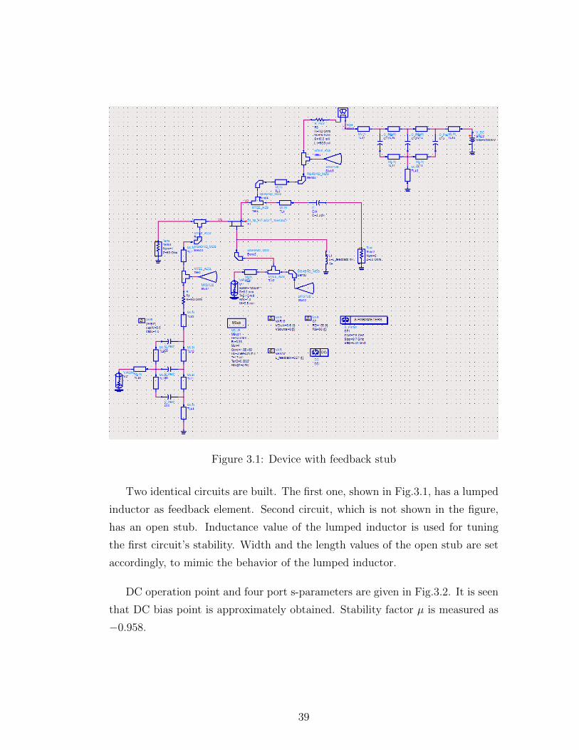
Figure 3.1: Device with feedback stub
Two identical circuits are built. The first one, shown in Fig.3.1, has a lumped
inductor as feedback element. Second circuit, which is not shown in the figure,
has an open stub. Inductance value of the lumped inductor is used for tuning
the first circuit’s stability. Width and the length values of the open stub are set
accordingly, to mimic the behavior of the lumped inductor.
DC operation point and four port s-parameters are given in Fig.3.2. It is seen
that DC bias point is approximately obtained. Stability factor µ is measured as
−0.958.
39

Figure 3.2: Stability analysis of the device with feedback
3.2.5 Electromagnetic Simulations and EM/Circuit Co-
Simulations
It is well known that, EM simulation results of printed microstrip structures could
deviate from that of RF simulation results. Depending on the application, it could
be imperative to run EM simulations on initial bias networks, and to update and
verify the circuit accordingly prior to design input and output matching networks.
Magnitude of the deviations between RF and EM simulations is observed to
reach up to the order of hundreds of MHz. Inconsistencies are mostly observed
in the simulation results of radial stubs that are used to provide RF chokes in
bias networks. Fringing field effects that are approximated in RF simulator are
ascribed for these.
Once the circuit’s configuration, operation point, and feedback structure that
makes the circuit optimally unstable -if necessary- are decided, the bias and
feedback networks should be characterized by EM simulations.
Even slight frequency, phase, or magnitude shifts in the behavior of these
networks, could make the stability of the device , hence the RF performance
could be significantly affected.
40
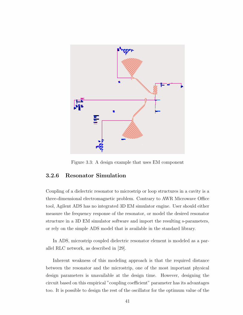
Figure 3.3: A design example that uses EM component
3.2.6 Resonator Simulation
Coupling of a dielectric resonator to microstrip or loop structures in a cavity is a
three-dimensional electromagnetic problem. Contrary to AWR Microwave Office
tool, Agilent ADS has no integrated 3D EM simulator engine. User should either
measure the frequency response of the resonator, or model the desired resonator
structure in a 3D EM simulator software and import the resulting s-parameters,
or rely on the simple ADS model that is available in the standard library.
In ADS, microstrip coupled dielectric resonator element is modeled as a par-
allel RLC network, as described in [29].
Inherent weakness of this modeling approach is that the required distance
between the resonator and the microstrip, one of the most important physical
design parameters is unavailable at the design time. However, designing the
circuit based on this empirical ”coupling coefficient” parameter has its advantages
too. It is possible to design the rest of the oscillator for the optimum value of the
41

coupling coefficient, without worrying about the phase noise degradation due to
suboptimal resonator coupling, which could be quite significant.
It should be noted that if the resonator is to be coupled to two parallel mi-
crostrips, ADS dielectric resonator model is not valid. In this case the alternative
to 3D EM simulation and physical measurement is using two transformers paral-
lel to simple parallel RLC model of the resonator, through which the resonator
couples to microstrips [20]. Turn ratios of the transformers define the coupling
coefficient values of the resonator to the microstrips.
In this work the simple ADS model is used for two reasons: 1) To exploit the
possibility of optimal design 2) To avoid complex and time consuming 3D EM
simulations.
Considering the fact that the frequency response is a function of the resonator
position, it is not viable to iterate spatially on the substrate through long EM
simulations, which leads to a virtually infinite number of simulations. Instead,
housing of the circuit is designed with two separate cavities which enable the
resonator measurements at the integration time, to compensate the lack of a
priori design information.
Loaded and unloaded Q factors of the resonator can be calculated using the
magnitude of the transmission coefficient of the resonator [29].
A quantity name x is defined in the following way
x(dB) = 3− 10log(1 + 10−0.1L0)
where x is added to minimum point of the insertion loss for the calculation of
loaded Q, and is subtracted from the maximum, ideally zero, for the calculation
o unloaded Q.
Dielectric resonator is simulated using the ADS model element, as explained
previously. As transmission line is terminated with its characteristic impedance,
length of it does not affect the coupling.
42

Substrate is chosen as Rogers RO4003C, with thickness of 12 mils. Resonant
frequency dependence on substrate dielectric constant and thickness is significant,
on the order of tens of MHz.
Resonator insertion loss is set to 6 dB by setting the coupling coefficient to 1
and x parameter defined above is obtained from the simulation results and given
in Fig.3.4.
Figure 3.4: Simulation results of the dielectric resonator coupled to microstrip
Simulation results suggest an unloaded Q of 5961 and a loaded Q of 2906.
3.2.7 Output Matching
As explained previously, satisfying the oscillation conditions and phase noise char-
acteristics depend on the input impedance of the active device, i.e. the impedance
seen by the resonator. Therefore both the amount of the negative resistance seen
in this port and its relation to the resonator’s reflection coefficient are of utmost
importance.
A simple formula for the design of output matching networks of oscillators is
43

to set the load resistance as one third of the negative resistance, and the load
reactance equal to negative reactance. This basic procedure is based on small
signal S-parameters analysis and hence does not account for the nonlinearity of
the device [20].
Apart from the fact that it is not possible to calculate power output and
harmonics levels beforehand using this method, it should be noted that the os-
cillation frequency usually deviates from its designated value due to the change
in the negative reactance by signal level. It is safe to say that the possibility
of the phase noise performance of the circuit to be suboptimal is quite high by
using this technique [20]. Therefore such small signal approaches should only be
utilized initially, if the design specifications require low phase noise.
In the resonator simulation subsection, it was shown that the frequency re-
sponse of the resonator has an optimum for the best phase noise. Although being
important, since the dielectric resonator is a passive device, its frequency response
does not have much degree of freedom. Previously it was shown that for the best
phase noise performance, reflection coefficients of resonator and the active device
should be orthogonal to cancel fluctuations induced between phase and ampli-
tude. In order to obtain such a relation, it is much useful to manipulate the
active device input impedance rather than that of resonator, which is essentially
a narrow band filter.
Output matching is thus the defining parameter for the oscillator. In the
experiment, 50 Ohm termination at the output port of the device is removed
and a large set of possible load impedances are swept via ”Parameter Sweep”
component, as shown in Fig.3.5.
Results show the input reflection coefficient values for each corresponding load
impedance. There is not much information on the literature about the optimum
negative resistance or conductance for the best phase noise. In [12], it is explained
that higher negative resistance or conductance is used if fast starting and high
output power are the design goals, whereas lower values result in better stability
and noise performance. It is also advised to use a moderate negative resistance
at the input port between -5 and -50 ohms, or between -0.2 and -0.02 mhos if
44

Figure 3.5: Output matching sweep simulation
negative conductance oscillator is being design. Negative resistance/conductance
should be maximally flat with frequency and with little or no reactance. So a
termination reflection coefficient is picked which provides sufficiently large input
reflection coefficient and has low reactance.
Output is then matched from the selected impedance to 50 Ohm. Following
the addition of the matching network, simulated input impedance and input
reflection coefficient of the device is shown in Fig.3.6.
Negative impedance is −21.256 + j5.185, which has a real part adequate for
the oscillation and small reactance.
45
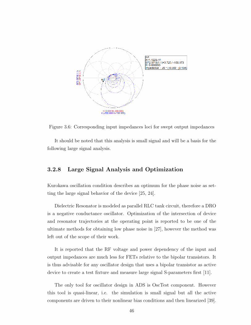
Figure 3.6: Corresponding input impedances loci for swept output impedances
It should be noted that this analysis is small signal and will be a basis for the
following large signal analysis.
3.2.8 Large Signal Analysis and Optimization
Kurokawa oscillation condition describes an optimum for the phase noise as set-
ting the large signal behavior of the device [25, 24].
Dielectric Resonator is modeled as parallel RLC tank circuit, therefore a DRO
is a negative conductance oscillator. Optimization of the intersection of device
and resonator trajectories at the operating point is reported to be one of the
ultimate methods for obtaining low phase noise in [27], however the method was
left out of the scope of their work.
It is reported that the RF voltage and power dependency of the input and
output impedances are much less for FETs relative to the bipolar transistors. It
is thus advisable for any oscillator design that uses a bipolar transistor as active
device to create a test fixture and measure large signal S-parameters first [11].
The only tool for oscillator design in ADS is OscTest component. However
this tool is quasi-linear, i.e. the simulation is small signal but all the active
components are driven to their nonlinear bias conditions and then linearized [39].
46

Instead of inserting OscTest tool between the resonator port and transistor
input port, resonator is simulated in small signal and active device is simulated in
large signal. Then, the large signal behavior of the active device is plotted onto
the resonator response and the circuit is tuned for optimum intersection, which
is defined as perpendicular [25, 14, 24].
Both resonator and active device reflection coefficients could be set using this
analysis method. Given simulation setup provides insight into the large signal
behavior of the device, which is invisible to the user if OscTest or a similar tool
is used.
Figure 3.7: Tuning of transistor input reflection coefficient
A simple illustration of this tuning procedure is given in Fig.3.7. The circle
represents the frequency response of the resonator. The lines intersecting the
circle represent the inverted reflection coefficients of the transistors, seen from
the port that is connected to the resonator. Each line corresponds to a circuit
with different parameters and is denoted by a number.
2 has the optimal value, that is perpendicular to the circle. 3 is on a different
bias point with all other parameters same, and 1 has a different output matching
47

network.
Note that however, the circle could be moved in clockwise or counter-clockwise
direction for any given specific transistor reflection coefficient trajectory by simply
adjusting the coupling microstrip’s length. Individual best matches of the lines 1
and 3 are still suboptimal and for the sake of simplicity they are not shown here.
Nyquist test results of the same circuits obtained with OscTest port between
9 and 10 GHz are shown in Fig.3.8.
Figure 3.8: Nyquist test results of the same tuning
Recalling that the Nyquist oscillation criteria is to encircle 1 + j0 point in
clockwise direction and the oscillation frequency is the point at which the trajec-
tory crosses the real axis; it is inferred that the circuit denoted by 1 is not going
to oscillate in given frequency range. However this circuit oscillates as the other
configurations, at 9.149 GHz frequency and with 9.1 dBm output power. Phase
noise comparison of these three versions is given in Fig.3.9. Phase noise of the
”optimal” version, denoted by 2, is better than others, around 10 dB.
As the example suggested, Nyquist test not only misleads about the circuit’s
oscillation, but also does not give any design feedback to the user. Two designs
that exhibit 10 dB residual phase noise difference have almost the same Nyquist
plots.
48
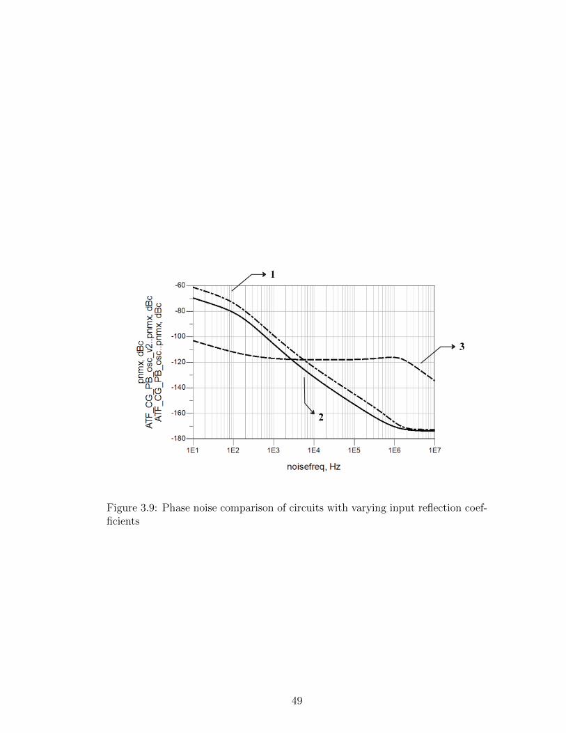
Figure 3.9: Phase noise comparison of circuits with varying input reflection coef-ficients
49
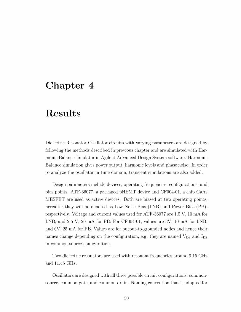
Chapter 4
Results
Dielectric Resonator Oscillator circuits with varying parameters are designed by
following the methods described in previous chapter and are simulated with Har-
monic Balance simulator in Agilent Advanced Design System software. Harmonic
Balance simulation gives power output, harmonic levels and phase noise. In order
to analyze the oscillator in time domain, transient simulations are also added.
Design parameters include devices, operating frequencies, configurations, and
bias points. ATF-36077, a packaged pHEMT device and CF004-01, a chip GaAs
MESFET are used as active devices. Both are biased at two operating points,
hereafter they will be denoted as Low Noise Bias (LNB) and Power Bias (PB),
respectively. Voltage and current values used for ATF-36077 are 1.5 V, 10 mA for
LNB; and 2.5 V, 20 mA for PB. For CF004-01, values are 3V, 10 mA for LNB;
and 6V, 25 mA for PB. Values are for output-to-grounded nodes and hence their
names change depending on the configuration, e.g. they are named VDS and IDS
in common-source configuration.
Two dielectric resonators are used with resonant frequencies around 9.15 GHz
and 11.45 GHz.
Oscillators are designed with all three possible circuit configurations; common-
source, common-gate, and common-drain. Naming convention that is adopted for
50

the distinction of oscillators is to use device-configuration-bias prefixes respec-
tively, e.g. ATF CS LNB, or CF4 CG PB.
4.1 Resonator Measurements
Although Agilent ADS accurately simulates the resonant frequency of a dielectric
resonator without the need of 3D EM simulation, manufacturing tolerances could
lead to frequency deviations. In critical applications tolerances could be kept
tight; however the cost would be higher in parallel.
MDR-24 series dielectric resonator is used from MCV Technologies. The res-
onator is reported to have an unloaded Q factor greater than 16000 at 10 GHz,
with dielectric constant between 24± 1. Frequency specification was conveyed to
the manufacturer as 9.6± 0.5 GHz, for the sake of low cost.
The measurements of the resonator showed that the resonant frequency is
around 9.15 GHz. Loaded and unloaded Q factor calculations described in [29]
are also given in Fig.4.1.
Figure 4.1: Measured resonator frequency response and quality factor calculations
In order to demonstrate the effect of shielding on quality factor and mechanical
51
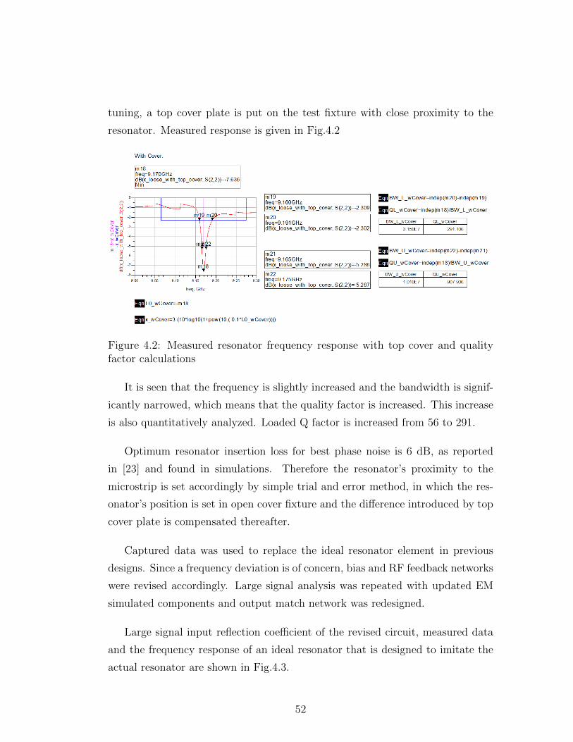
tuning, a top cover plate is put on the test fixture with close proximity to the
resonator. Measured response is given in Fig.4.2
Figure 4.2: Measured resonator frequency response with top cover and qualityfactor calculations
It is seen that the frequency is slightly increased and the bandwidth is signif-
icantly narrowed, which means that the quality factor is increased. This increase
is also quantitatively analyzed. Loaded Q factor is increased from 56 to 291.
Optimum resonator insertion loss for best phase noise is 6 dB, as reported
in [23] and found in simulations. Therefore the resonator’s proximity to the
microstrip is set accordingly by simple trial and error method, in which the res-
onator’s position is set in open cover fixture and the difference introduced by top
cover plate is compensated thereafter.
Captured data was used to replace the ideal resonator element in previous
designs. Since a frequency deviation is of concern, bias and RF feedback networks
were revised accordingly. Large signal analysis was repeated with updated EM
simulated components and output match network was redesigned.
Large signal input reflection coefficient of the revised circuit, measured data
and the frequency response of an ideal resonator that is designed to imitate the
actual resonator are shown in Fig.4.3.
52
Figure 4.3: Large signal analysis of the device with measured resonator response
It is seen that the intersection is approximately set for optimum. Harmonic
Balance simulation results show the oscillation at 9.162 GHz, with phase noise
performance consistent with the oscillator designed by using ideal resonator
model. Therefore the measurement results are used for further simulations de-
scribed in this chapter.
4.2 Comparison of Devices, Circuit Configura-
tions, and Bias
Simulation results of oscillators that are designed for operation at 9.15 GHz are
summed in Table 4.1. fosc and ftran denote to the oscillation frequency (GHz),
calculated by Harmonic Balance simulator and Transient simulator, respectively.
H1 is power output and H2 is the level of second harmonic (both in dBm). The
last four columns denote the phase noise levels at given frequency offsets (in
dBc/Hz).
CF004-01 device did not oscillate in common drain configuration, while ATF-
36077 oscillated. However, these common drain oscillators have poor phase
53

Table 4.1: Phase Noise Performance Comparisons
Osc fosc ftran H1 H2 @100Hz @1kHz @10kHz @100kHz
ATF CD LNB 9.150 9.228 -1.7 -14.5 -50.2 -61.0 -80.8 -100.8ATF CD PB 9.150 9.207 5.208 -7.996 -40.4 -60.2 -80.2 -100.1ATF CS LNB 9.151 9.313 1.7 -14.7 -74.8 -100 -126.5 -148.5ATF CS PB 9.332 9.398 7.5 -26.2 -37.1 -54.1 -73.7 -93.74
ATF CG LNB 9.150 9.139 3.7 -20.8 -77.0 -100.5 -125.3 -146.2ATF CG PB 9.150 9.140 10.0 -12.8 -80.9 -105.7 -131.5 -153.0CF4 CD LNB - - - - - - - -CF4 CD PB - - - - - - - -CF4 CS LNB 9.150 9.140 -3.7 -27.3 -86.7 -106.8 -126.8 -146.8CF4 CS PB 9.150 9.145 12.2 -21.6 -95.1 -114.0 -134.3 -154.2
CF4 CG LNB 9.150 9.171 0.5 -21.9 -94.6 -111.3 -126.0 -145.9CF4 CG PB 9.151 9.142 3.0 -25.3 -96.5 -113.5 -127.2 -147
noise performance in both LNB and PB conditions. Relatively larger differ-
ence observed between the fosc and ftran frequencies could be an indicator of a
frequency shift due to increased nonlinearity level. A similar effect is observed in
ATF CS PB device. Oscillation frequency calculated by Harmonic Balance and
Transient simulations are close, yet away from the resonance frequency. As in the
case of CD oscillators, phase noise is quite high.
Common gate configuration shows good phase noise performance for both
devices and for both bias points. Best phase noise performance away from the
carrier is that of CF4 CS PB, however the close-in noise performances of CG
configurations are slightly better.
4.3 Effect of Resonator Coupling on Phase
Noise
Everard’s phase noise model defines an optimum for the ratio of the loaded Q to
the unloaded Q [23]. Phase noise is lowest for the resonator insertion loss value of
6 dB. According to their observations, phase noise degrades for higher and lower
insertion loss values, approximately linearly on a dB scale. At higher than 6 dB
54

insertion loss region, slope of the degradation is approximately 0.75, at lower than
6 dB insertion loss region the slope is approximately 4.
Resonator coupling simulation experiment results are consistent with findings
of [23]. In Fig.4.4, phase noise performances of identical common-drain oscillator
circuits with varying coupling coefficients are shown. Optimal value for insertion
loss is found as 6 dB.
Figure 4.4: Simulated phase noise vs. resonator insertion loss
4.4 Large Signal Optimization
Simulation results clearly demonstrates the optimality of the phase noise perfor-
mance depending on the coupling characteristics. Fig.4.5 shows the intersections
of large signal input reflection coefficient trajectories and resonator response de-
pending on the coupling line length. Corresponding phase noise results are listed
in Table 4.2.
55

Figure 4.5: Varying coupling simulation results
56

Table 4.2: Phase Noise Degradation Depending on the Intersection Angles
Line Length in mm PN @100 kHz (dBc/Hz) PN Deviation(dB)
9 -127 -199.6 -140 -610.2 -145 -110.6 -146 011.2 -144 -211.6 -140 -612.2 -133 -1312.6 -129 -18
This tuning process has two degrees of freedom, which are proximity of the
resonator to the coupling microstrip and to the active device. Such a tuning pro-
cedure could be implemented when the oscillator is being built by experimentally
changing the dielectric resonator’s position. It should be noted however that,
tuning of these two parameters do not necessarily result in optimum phase noise
performance since the input reflection coefficient could not be measured or tuned
in this approach. Results of suboptimal input reflection coefficient are illustrated
in the previous chapter.
Large signal behavior of the transistor’s input reflection coefficient is tuned
by output matching network, RF feedback stubs if any, and bias point.
4.5 Low Frequency Feedback Techniques
4.5.1 Output-to-Input Low Frequency Feedback
Adding a Low Pass Filter (LPF) in the oscillation loop is reported to reduce the
phase noise by suppressing the low frequency noise [24, 34].
Three identical oscillators with LPF networks inserted between Drain and
Source terminals are simulated. Cut-off frequencies are varied as shown in Fig.4.6.
Phase noise performances of these oscillators with feedback are significantly better
than that of the one without feedback and are close to each other.
57
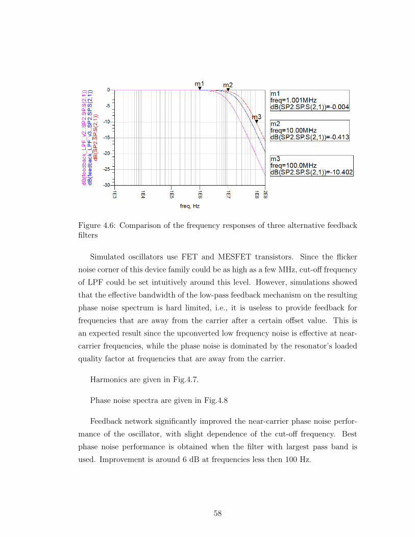
Figure 4.6: Comparison of the frequency responses of three alternative feedbackfilters
Simulated oscillators use FET and MESFET transistors. Since the flicker
noise corner of this device family could be as high as a few MHz, cut-off frequency
of LPF could be set intuitively around this level. However, simulations showed
that the effective bandwidth of the low-pass feedback mechanism on the resulting
phase noise spectrum is hard limited, i.e., it is useless to provide feedback for
frequencies that are away from the carrier after a certain offset value. This is
an expected result since the upconverted low frequency noise is effective at near-
carrier frequencies, while the phase noise is dominated by the resonator’s loaded
quality factor at frequencies that are away from the carrier.
Harmonics are given in Fig.4.7.
Phase noise spectra are given in Fig.4.8
Feedback network significantly improved the near-carrier phase noise perfor-
mance of the oscillator, with slight dependence of the cut-off frequency. Best
phase noise performance is obtained when the filter with largest pass band is
used. Improvement is around 6 dB at frequencies less then 100 Hz.
58

Figure 4.7: Harmonic Balance simulation results of the oscillator circuit withLPF feedback
Phase noise simulation tools in modern CAD tools are reported to give accu-
rate and consistent results [39, 42]. In [42], difference between phase noise sim-
ulations and measurements are found to be insignificant at frequencies greater
than 1 kHz offset.
Although introducing low pass feedback network to the oscillation loop is a
known method, it could be argued that the accuracy of the simulation of near-
carrier phase noise improvement would be limited; considering the fact that man-
ufacturers usually don’t provide flicker noise corner data and measuring flicker
noise could be impractical because of the need for advanced instruments and com-
plicated test fixture. However the results indicate that the improvement exceeds
40 dB at its most; is greater than 10 dB at 1 kHz offset, and gradually decays to
1 dB up to 10 kHz offset. So even if the improvement is erroneously calculated at
lower offset frequencies due to simulator incapability, it is still significant in the
1-10 kHz bandwidth, in which the simulator is known to work accurately [42].
59
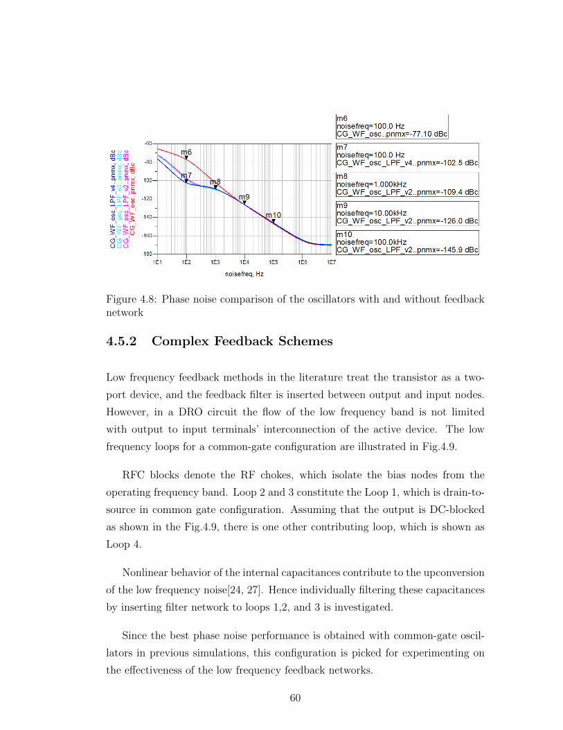
Figure 4.8: Phase noise comparison of the oscillators with and without feedbacknetwork
4.5.2 Complex Feedback Schemes
Low frequency feedback methods in the literature treat the transistor as a two-
port device, and the feedback filter is inserted between output and input nodes.
However, in a DRO circuit the flow of the low frequency band is not limited
with output to input terminals’ interconnection of the active device. The low
frequency loops for a common-gate configuration are illustrated in Fig.4.9.
RFC blocks denote the RF chokes, which isolate the bias nodes from the
operating frequency band. Loop 2 and 3 constitute the Loop 1, which is drain-to-
source in common gate configuration. Assuming that the output is DC-blocked
as shown in the Fig.4.9, there is one other contributing loop, which is shown as
Loop 4.
Nonlinear behavior of the internal capacitances contribute to the upconversion
of the low frequency noise[24, 27]. Hence individually filtering these capacitances
by inserting filter network to loops 1,2, and 3 is investigated.
Since the best phase noise performance is obtained with common-gate oscil-
lators in previous simulations, this configuration is picked for experimenting on
the effectiveness of the low frequency feedback networks.
60

Figure 4.9: Low Frequency Loops in a Common-Gate DRO Circuit
Two types of filters are used. In order not to affect the bias point, both
are designed with DC-blocking functionality. The former is a pure Low-Pass
Filter shown in Fig.4.10, while the latter is essentially a High-Pass Filter with a
nonuniform stop-band. Frequencies up to 100 Hz are attenuated lightly, higher
frequencies below MHz band are attenuated more with peak attenuation around
100 kHz. Frequency response of this filter is given in 4.11.
Figure 4.10: Frequency Response of the Feedback Low-Pass Filter
Simulations are done by implementing feedback filters between drain-to-source
(DS), drain-to-gate (DG), and source-to-gate (SG) nodes. Each node is either left
61

Figure 4.11: Frequency Response of the Feedback Band-Pass Filter
open, or LPF is connected, or BPF is connected. All 27 possible combinations
for a single oscillator are simulated. Due to the large number of simulations, a
single oscillator is picked for the task.
Combinations are enumerated for the sake of simplicity, and a reference table
listing the corresponding feedback filter structures is provided in the Appendix,
in Table A.1.
CF4 CG PB design is simulated at both 9.15 GHz and 11.45 GHz frequencies
with varying feedback filters. Simulation results at 9.15 GHz are summarized in
Table 4.3. Max. Imp denotes the maximum improvement observed in phase noise
with regard to the original oscillator, Freq. denotes the frequency at which the
maximum improvement is observed. The last three columns denote the phase
noise levels at given offset frequencies.
Simulation results at 11.45 GHz are summarized in Table 4.4.
Low pass filtering reduced the loop gain of low frequencies and hence sup-
pressed the upconversion originated phase noise. This result is consistent with
findings reported in the literature.
62

Table 4.3: Performance Comparison of Feedback Networks at 9.15 GHz
Version Max. Imp. Freq. @100Hz @1kHz @10kHz
1 21.1 1 19.4 8.3 1.52 34.4 1 23.5 8.1 1.43 16.9 4 8.9 -1.2 0.14 31.6 1 10.5 -1 0.15 30.5 1 22.6 7.33 1.16 37.5 1 24.8 8.5 1.57 19.4 63.1 18.9 7.9 1.38 30.5 1 19.8 7.9 1.39 30.9 7.9 23.4 7.6 1.310 32.7 12.6 23.8 7.5 1.311 28.2 28.2 18.2 7.7 1.312 35.7 1 23.8 7.5 1.313 23.5 3.1 18.8 7.8 1.314 34.0 6.3 23.8 7.5 1.315 32.5 1 24.1 7.5 1.316 37.5 1 23.9 7.5 1.317 37.0 1 24.3 7.5 1.318 40.6 1 24 7.5 1.319 30.7 1 22.3 7.6 1.320 36.7 1 23.9 7.5 1.321 26.7 10 22.3 7.7 1.322 36.4 1 24 7.5 1.323 35.3 6.3 23.9 7.5 1.324 40.1 1 24 7.5 1.325 34.7 7.9 23.9 7.5 1.326 46.0 1 24.1 7.5 1.3
Additional indication of the simulation results is that, incorporation of BPFs
provided a better improvement in the phase noise performance, significant in
some cases. This improvement could be ascribed to further reduction of the loop
gain due to attenuating low frequency bands using BPFs on the feedback path.
The most effective feedback path is drain-to-source connection, which is the
output-to-input path for the simulated common gate configuration. However,
the improvement provided by implementing additional feedback networks could
exceed 10 dB.
63
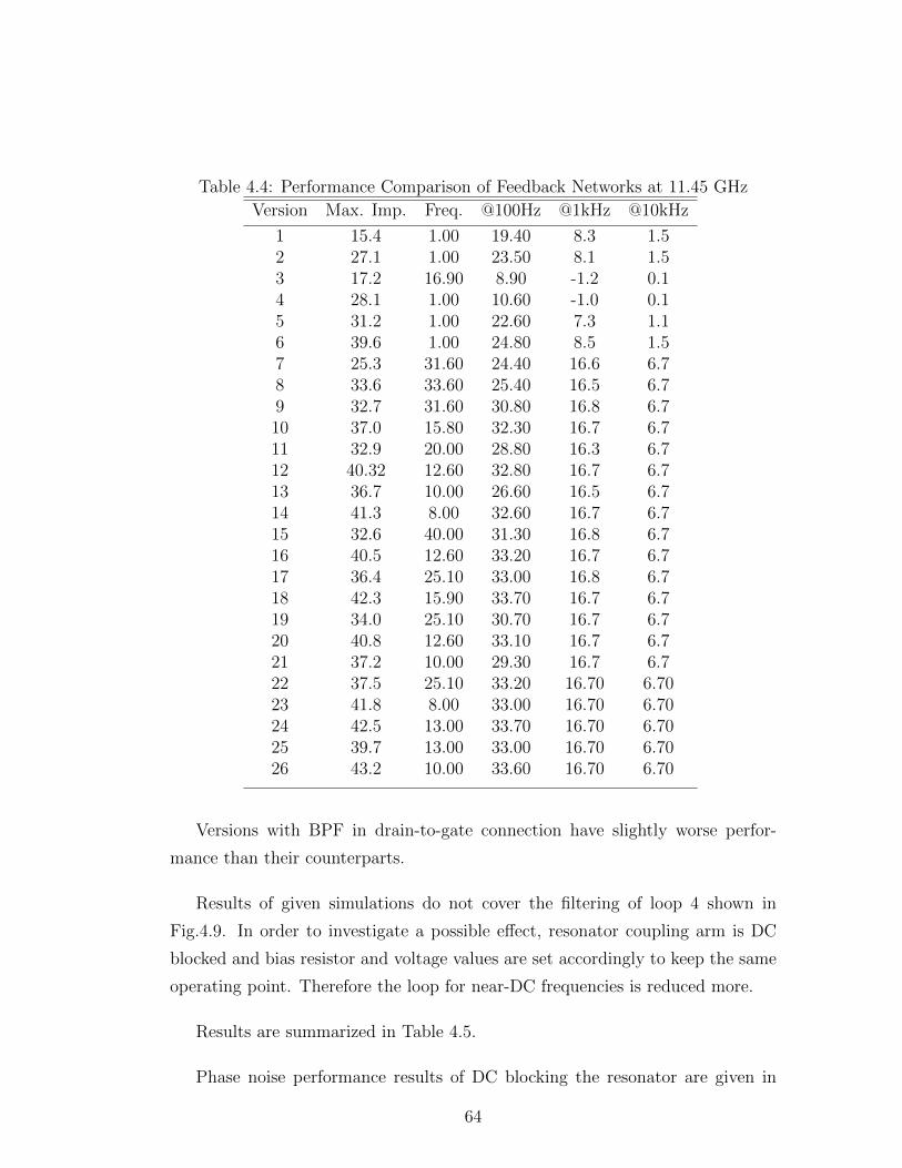
Table 4.4: Performance Comparison of Feedback Networks at 11.45 GHz
Version Max. Imp. Freq. @100Hz @1kHz @10kHz
1 15.4 1.00 19.40 8.3 1.52 27.1 1.00 23.50 8.1 1.53 17.2 16.90 8.90 -1.2 0.14 28.1 1.00 10.60 -1.0 0.15 31.2 1.00 22.60 7.3 1.16 39.6 1.00 24.80 8.5 1.57 25.3 31.60 24.40 16.6 6.78 33.6 33.60 25.40 16.5 6.79 32.7 31.60 30.80 16.8 6.710 37.0 15.80 32.30 16.7 6.711 32.9 20.00 28.80 16.3 6.712 40.32 12.60 32.80 16.7 6.713 36.7 10.00 26.60 16.5 6.714 41.3 8.00 32.60 16.7 6.715 32.6 40.00 31.30 16.8 6.716 40.5 12.60 33.20 16.7 6.717 36.4 25.10 33.00 16.8 6.718 42.3 15.90 33.70 16.7 6.719 34.0 25.10 30.70 16.7 6.720 40.8 12.60 33.10 16.7 6.721 37.2 10.00 29.30 16.7 6.722 37.5 25.10 33.20 16.70 6.7023 41.8 8.00 33.00 16.70 6.7024 42.5 13.00 33.70 16.70 6.7025 39.7 13.00 33.00 16.70 6.7026 43.2 10.00 33.60 16.70 6.70
Versions with BPF in drain-to-gate connection have slightly worse perfor-
mance than their counterparts.
Results of given simulations do not cover the filtering of loop 4 shown in
Fig.4.9. In order to investigate a possible effect, resonator coupling arm is DC
blocked and bias resistor and voltage values are set accordingly to keep the same
operating point. Therefore the loop for near-DC frequencies is reduced more.
Results are summarized in Table 4.5.
Phase noise performance results of DC blocking the resonator are given in
64

Table 4.5: Performance Comparison of Feedback Networks at 11.45 GHz whenDR is DC blocked
Version Max. Imp. Freq. @100Hz @1kHz @10kHz
1 15.6 63.1 15.3 5.0 0.42 26.0 20 20.2 4.6 0.33 2.8 50.1 2.2 -0.3 -0.14 8.1 15.8 2 -0.4 -0.15 20.0 39.8 18.6 4.8 0.26 28.5 20 21.7 5 0.37 15.3 63.1 15.1 5.1 0.28 16.3 31.6 15.6 5 0.29 24.6 25.1 20 4.7 0.210 25.9 25.1 20.9 4.6 0.211 19.8 31.6 17.1 4.9 0.212 27.9 20 21.1 4.6 0.213 19.2 15.8 15.7 5 0.214 27.5 15.8 21 4.6 0.215 22.7 39.8 20.9 4.6 0.216 28.8 20 21.3 4.6 0.217 27.5 20 21.4 4.6 0.218 31.1 15.8 21.4 4.5 0.219 22.6 31.6 20 4.7 0.220 28.7 20 21.2 4.7 0.221 22.1 20 19.1 4.7 0.222 27.7 20 21.3 4.6 0.223 28.5 15.8 21.2 4.6 0.224 31.1 15.8 21.4 4.5 0.225 28.0 20 21.2 4.6 0.226 31.0 12.6 21.4 4.5 0.2
Fig.4.12 and Fig.4.13.
Improvement in close-in phase noise is observed in both cases. This result is
consistent with the low frequency loop approach adopted, since DC blocking the
resonator without altering the device operating point is effectively filtering low
frequency components in loop 4, as illustrated in Fig.4.9
Also a residual phase noise improvement around 6 dB is observed at 9.15 GHz.
In order to investigate the effect of attenuation amount of the low frequencies,
65
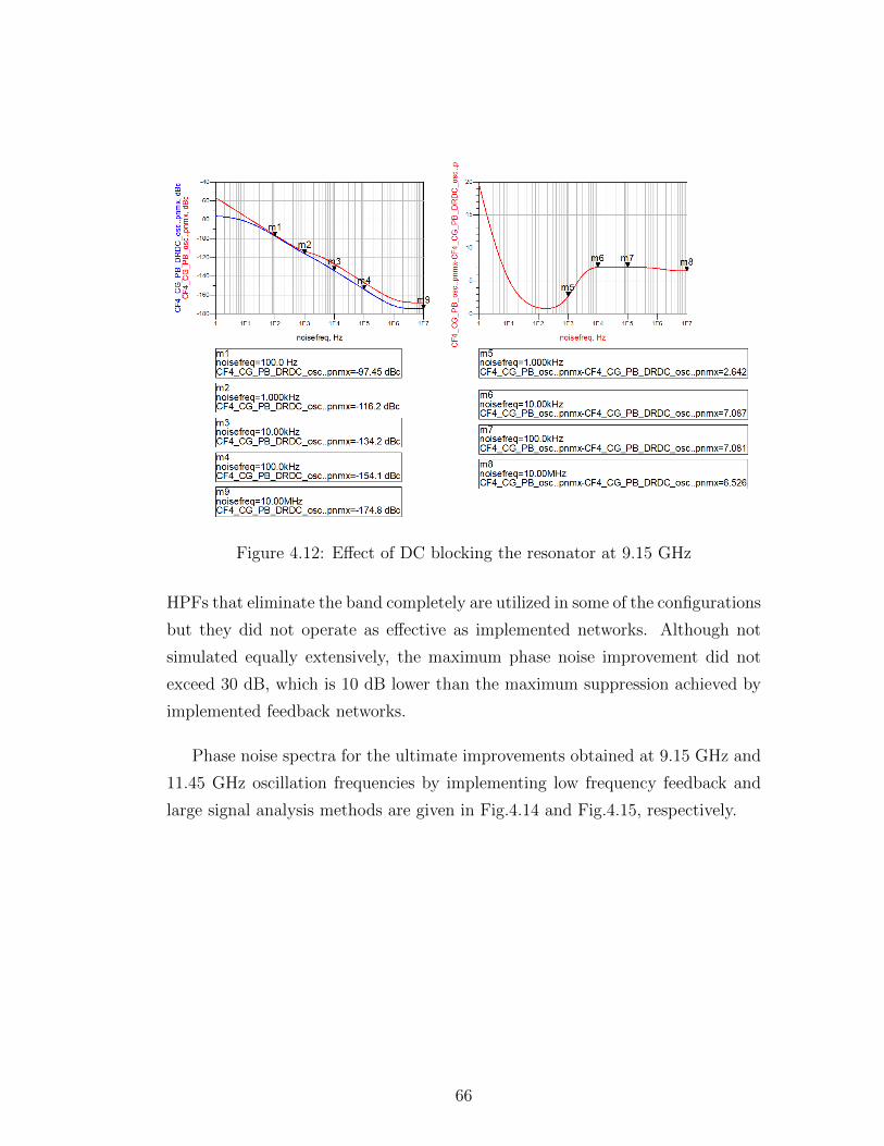
Figure 4.12: Effect of DC blocking the resonator at 9.15 GHz
HPFs that eliminate the band completely are utilized in some of the configurations
but they did not operate as effective as implemented networks. Although not
simulated equally extensively, the maximum phase noise improvement did not
exceed 30 dB, which is 10 dB lower than the maximum suppression achieved by
implemented feedback networks.
Phase noise spectra for the ultimate improvements obtained at 9.15 GHz and
11.45 GHz oscillation frequencies by implementing low frequency feedback and
large signal analysis methods are given in Fig.4.14 and Fig.4.15, respectively.
66

Figure 4.13: Effect of DC blocking the resonator at 11.45 GHz
Figure 4.14: Maximum Phase Noise Improvement at 9.15 GHz
67

Figure 4.15: Maximum Phase Noise Improvement at 11.45 GHz
68

Chapter 5
Conclusion
A DRO design is presented using nonlinear device models and resonator measure-
ments. Extensive simulations are done in order to understand the configuration,
circuit and parameter dependencies of phase noise performance.
Large signal analysis method that defines an optimum at an abstraction level
is realized within an RF and Electromagnetic co-simulation environment, and
parameter dependencies are illustrated. Frequency response of two dielectric
resonators with different resonant frequencies are measured by using a microstrip
coupling test fixture. Measurement results are shown to be in agreement with
the ideal resonator models. Measured data is imported into the RF/EM co-
simulation environment and used as input to Harmonic Balance simulation of the
oscillator. Resonator coupling parameters are shown to be significant on phase
noise performance of the oscillator. Simulation results of oscillator circuits both
with ideal resonator models and imported measurement data are shown to be
consistent with optimum coupling parameters suggested in the literature.
Simulation structure for testing and implementing the optimum phase noise
performance condition defined in Kurokawa model is proposed and explained. Us-
ing these simulation steps; phase noise is shown to be suppressed up to 20 dB at
100 kHz offset, at 9.15 GHz. Suboptimal designs are compared with the best case
69

in terms of Kurokawa condition, and they are shown to have varying character-
istics while being indifferent to Nyquist criterion. Therefore it was demonstrated
by simulation that the proposed design method contributes to improve the design
of oscillator circuits.
Low frequency feedback technique which constitutes a significant improvement
method in phase noise reduction is implemented and tried. Improvements in
close-in phase noise performance are observed in simulation results. The essential
low frequency feedback method that is reported in the literature is adding low
pass filter, which essentially stabilizes -or limits- the low-frequency gain, between
output and input ports of the circuit. This simple procedure is implemented and
results are reported. In addition to this method, further filtering is implemented
and simulated between all three ports of the transistor in order to investigate the
suppression effect on the nonlinear capacitances of the transistor. Results suggest
that additional filtering improves the phase noise performance further, around 10
dB.
Although a generalized method that is reproducible for every device or process
is still not available, the methods presented cover the evaluation of design steps
that are needed to be checked in order to obtain low phase noise. It can be
concluded that, designing a low phase noise oscillator is a process that heavily
depends on the careful analysis of the characteristics of used active device.
It is believed that use of a load pull device or similar equipment for the
purpose of accurately characterizing and setting as required the input impedance
of the transistor would be greatly beneficial, since the performance of the circuit
is highly dependent on proper input and output matching.
Also it should be noted that the use of layout components that are EM sim-
ulated in Agilent Momentum, gives different phase noise results than using mi-
crostrip components in Agilent ADS that have identical frequency responses, up
to 8 dB. A possible reason for such behavior is the undefined near DC behavior
of RF simulation components. Therefore apart from the accuracy concerns, EM
components should be used in EM/Co-circuit simulations in order to accurately
analyze low frequency behavior of the whole circuit.
70

The method for designing an oscillator with low phase noise both close and
away from the carrier is developed and presented. By implementing low frequency
networks, significant improvement is observed in close-in frequencies. Combined
with the optimization for Kurokawa condition, better residual phase noise per-
formance is obtained in whole spectrum of phase noise, as high as 45 dB, both at
9.15 GHz and 11.45 GHz.
Effects of the parameters of implemented low frequency feedback networks on
phase noise performance could be further investigated in the future.
71
Bibliography
[1] R. P. J. Graffeuil, “Low frequency noise properties of microwave transistors
and their application to circuit design,” 24th European Microwave Confer-
ence, vol. 1, pp. 62–75, 1994.
[2] E. Rubiola, Phase Noise and Frequency Stability in Oscillators. Cambridge,
UK: Cambridge University Press, 2009.
[3] J. Johnson, “The schottky effect in low frequency circuits,” Physical Review,
vol. 26, no. 1, pp. 71–85, 1925.
[4] M. Planat, Noise, Oscillator and Algebraic Randomness From Noise in Com-
munications to Number Theory. Berlin Heidelberg: Springer-Verlag, 1999.
[5] S. Watanabe, “Multi-lorentzian model and 1/f noise spectra,” Journal of the
Korean Physical Society, vol. 3, pp. 646–650, 2005.
[6] Y. J. P. Sung-Min Hong, Chan Hyeong Park and H. S. Min, “Physics-based
analysis and simulation of 1/f noise in mosfets under large-signal operation,”
IEEE Transactions on Electron Devices, vol. 57, pp. 1110 – 1118, 2010.
[7] C. F. Pier Andrea Traverso, “An empirical bipolar device nonlinear noise
modeling approach for large-signal microwave circuit analysis,” IEEE Trans-
actions on Microwave Theory and Techniques, vol. 54, no. 12, pp. 4341–4352,
2006.
[8] E. S. Ferre-Pikal and F. H. Savage, “Up-converted 1/f pm and am noise in
linear hbt ampliers,” IEEE Transactions on Ultrasonics, Ferroelectrics, and
Frequency Control, vol. 55, no. 8, pp. 1698–1704, 2008.
72

[9] T. H. Morshed and M. V. Dunga, “Compact modeling of flicker noise vari-
ability in small size mosfets,” Electron Devices Meeting (IEDM), 2009 IEEE
International, pp. 1–4, 2009.
[10] K. S. Svetlana A. Vitusevich, “Design and characterization of an all-
cryogenic low phase-noise sapphire k-band oscillator for satellite communi-
cation,” IEEE Transactions on Microwave Theory and Techniques, vol. 51,
no. 1, pp. 163–169, 2003.
[11] A. K. P. Ulrich L. Rohde and G. Boeck, The Design of Modern Microwave
Oscillator for Wireless Applications. Hoboken, New Jersey: John Wiley &
Sons, 2005.
[12] R. W. Rhea, Discrete Oscillator Design Linear, Nonlinear, Transient, and
Noise Domains. Norwood, MA: Artech House, 2010.
[13] C. B. J.K.A. Everard, “Reduced transposed flicker noise in microwave os-
cillators using gaas-based feedforward amplifiers,” IEEE Transactions on
Ultrasonics, Ferroelectrics and Frequency Control, vol. 54, no. 6, pp. 1108 –
1117, 2007.
[14] R. G. Rogers, Low Phase Noise Microwave Oscillator Design. Norwood,
MA: Artech House, 1991.
[15] R. W. Rhea. personal communication.
[16] A. K. P. Ulrich L. Rohde, “Tunable active inductor offers integrable and
cost-effective alternatives of varactor tuned vcos,” Frequency Control Sym-
posium, 2009 Joint with the 22nd European Frequency and Time forum.
IEEE International, pp. 962–967, 2009.
[17] A. A. A. Emad Hegazi, “Varactor characteristics, oscillator tuning curves,
and amfm conversion,” IEEE Journal of Solid-State Circuits, vol. 38, no. 6,
pp. 1033–1039, 2003.
[18] J. N. A. Victor, “Noise characteristics of an oscillator with a barium stron-
tium titanate (bst) varactor,” IEE Proceedings on Microwaves, Antennas
and Propagation, vol. 153, no. 1, pp. 96–102, 2006.
73
[19] D. Leeson, “A simple model of feedback oscillator noise spectrum,” Proceed-
ings of the IEEE, vol. 54, pp. 329–330, 1966.
[20] G. Gonzalez, Foundations of Oscillator Circuit Design. Norwood, MA:
Artech House, 2007.
[21] W. Robins, Phase Noise in Signal Sources. Herts, UK: The Institution of
Engineering and Technology, 1982.
[22] T. L. A. Hajimiri, “A general theory of phase noise in electrical oscillators,”
IEEE Journal of Solid-State Circuits, vol. 33, no. 2, pp. 179–194, 1998.
[23] J. Everard, Fundamentals of RF Circuit Design with Low Noise Oscillators.
Hoboken, New Jersey: John Wiley & Sons, 2001.
[24] A. Grebennikov, RF and Microwave Transistor Oscillator Design. Hoboken,
New Jersey: John Wiley & Sons, 2007.
[25] K. Kurokawa, “Some basic characteristics of broadband negative resistance
oscillator circuits,” Bell System Technical Journal, vol. 48, no. 6, pp. 1937–
1955, 1969.
[26] J. Piekarski and K. Czuba, “The method of designing ultra low phase noise
dielectric resonator oscillators,” 18th International Conference on Microwave
Radar and Wireless Communications (MIKON), pp. 1–4, 2010.
[27] C.-Y. S. Hans Rohdin and C. Stolte, “A study of the relation between device
low-frequency noise and oscillator phase noise for gaas mesfets,” Microwave
Symposium Digest, 1984 IEEE MTT-S International, pp. 267–269, 1984.
[28] M. Golio and J. Golio, RF and Microwave Passive and Active Technologies.
Boca Raton, FL: CRC Press, 2008.
[29] D. Kajfez and P. Guillon, Dielectric Resonators. Norwood, MA: Artech
House, 1986.
[30] R. D. Richtmyer, “Dielectric resonators,” Journal of Applied Physics, vol. 10,
no. 6, pp. 391–398, 1939.
74

[31] M. T. Sebastian, Dielectric Materials for Wireless Communication. Amster-
dam, Netherlands: Elsevier BV, 2008.
[32] K. Y. Mark M. Nelson and M. Thomason, “Efficacy of fluorine doping at
various stages on noise reduction,” 2005 IEEE Workshop on Microelectronics
and Electron Devices, pp. 17–20, 2005.
[33] E. N. Ivanov and M. E. Tobar, “Low phase-noise sapphire crystal mi-
crowave oscillators: current status,” IEEE Transactions on Ultrasonics, Fer-
roelectrics, and Frequency Control, pp. 263–269, 2009.
[34] I. Ibrahim and H. Heuermann, “Improvements in the flicker noise reduc-
tion technique for osillator designs,” European Microwave Conference 2009,
pp. 1215 – 1218, 2009.
[35] J. J. Majewski, “New method of phase noise and intermodulation distor-
tion reduction in high-order qam systems,” 13th International Conference
on Microwaves, Radar and Wireless Communications MIKON-2000, vol. 1,
pp. 258–264, 2000.
[36] M. Prigent and J. Obregon, “Phase noise reduction in fet oscillators by low-
frequency loading and feedback circuitry optimization,” IEEE Transactions
on Microwave Theory and Techniques, vol. 35, no. 3, pp. 349–352, 1987.
[37] C. Sanabria, Noise of AlGaN/GaN HEMTs and Oscillators. PhD thesis,
University of California Santa Barbara, 2006.
[38] A. M. P. George D. Vendelin and U. L. Rohde, Microwave Circuit Design
Using Linear and Nonlinear Techniques. Hoboken, New Jersey: John Wiley
& Sons, 2005.
[39] F. Kusidlo. personal communication.
[40] J. Gao and G. Boeck, “Relationships between common source, common gate,
and common drain fets,” IEEE Transactions on Microwave Theory and Tech-
niques, vol. 53, no. 12, pp. 3825–3831, 2005.
[41] “Design considerations for a ku-band dro in digital communication systems,”
Tech. Rep. AN1035, California Eastern Laboratories, April 2003.
75

[42] M. X. Jeremy Everard and S. Bale, “Simplified phase noise model for
negative-resistance oscillators and a comparison with feedback oscillator
models,” IEEE Transactions on Ultrasonics, Ferroelectrics, and Frequency
Control, vol. 59, no. 3, pp. 382–390, 2012.
76

Appendix A
Feedback Configurations
Feedback networks implemented in circuits are defined in Table A.1. L and B
stand for LPF and BPF, respectively.
77

Table A.1: Feedback Networks Implemented
Version DS DG SG
1 - - L2 - - B3 - L -4 - B -5 L - -6 B - -7 - L L8 - B L9 - L B10 - B B11 L L -12 B L -13 L B -14 B B -15 L - L16 B - L17 L - B18 B - B19 L L L20 B L L21 L B L22 L L B23 B B L24 B L B25 L B B26 B B B
78