low energy communication: nanophotonic & electrical prof ... · read the current going through...
TRANSCRIPT

Low Energy Communication:
NanoPhotonic & Electrical
Prof. Eli Yablonovitch
EECS Dept.
UC Berkeley

What is the energy cost of reading out your flash memory?

( )
( )
processedbitperkT40~ConsumedEnergy
fkT4qkT2fq2iVpowerRequired
fq2i
fq2i
fiq2iRatioNoisetoSignal
mVolts50~q/kT2iRVvoltageRequired
NoiseJohnson..........fRkT4i
NoiseShot...........fiq2i
2
2
∆×=×∆>
∆×>
∆=
∆=−−
>>=
∆×=∆
∆×=∆
Read the current going through a resistor, in the presence of noise:
With a safety margin:

Units:
~40kT/bit of information
0.016 atto-Joules/bit of information
0.16 nano-Watts/Gbit/second
This is about 106 times better than we are doing today!

There are many type of memory possible:1. Flash2. SRAM3. Dram4. Magnetic Spin5. Nano-Electro-Chemical Cells6. Nano-Electro-Mechanical NEMS7. Moletronic8. Chalcogenide glass (phase change)9. Carbon Nanotubes
••
Similarly there are many ways to do logic.
But there are not many ways to communicate:
1. Microwaves (electrical)2. Optical 5

What will be the energy cost, per bit processed?
1. Logic energy cost ~40kT per bit processed
2. Storage energy cost ~40kT per bit processed
3. Communications currently >100,000kT per bit processed
.
6

fkTR
V
fRkTV
noise
noise
∆=
∆=
4
42
2
What is the energy cost for electrical communication?
Signal Noise PowerEnergy per bit≥ = 4kT per bit
All information processing costs ~ 40kT per bit. (for good Signal-to-Noise Ratio)
Great!
So what’s the problem?

mVolt1V
CqqkT4VCq
qkT4V
C1kT4V
RC1RkT4V
fRkT4V
Volts10mVolts100noise
2noise
2noise
2noise
2noise
≈
×=
×=
×=
=
∆=
µ
//321
The natural voltage range for wired communication is rather low:
The thermally activated device wants at least one electron at ~1Volt.
The wire wants1000 electrons at 1mVolt each.
(to fulfill the signal-to-noise requirement >1eV of energy)
Voltage Matching Crisis at the nano-scale!
If you ignore it the penalty will be (1Volt/1mVolt)2 = 106
The natural voltage range for a thermally activated switch like transistors is >>kT/q, eg. ~ 40kT/q
or about ~1Volt

10µm
1µm
100nm
10nm
Moore's Law
1960 1980 2000
Crit
ical
D
imen
sion
2020 2040 2060Year
Tech
nolo
gy G
ap
Gates only
Gates including wires
107
105
102
1
0.1
104
106
10
108
103
Ene
rgy
per B
it fu
nctio
n (k
T)
The other , for energy per bit function
Shoorideh and Yablonovitch, UCLA 2006
Transistor Measurements by Robert Chau, Intel
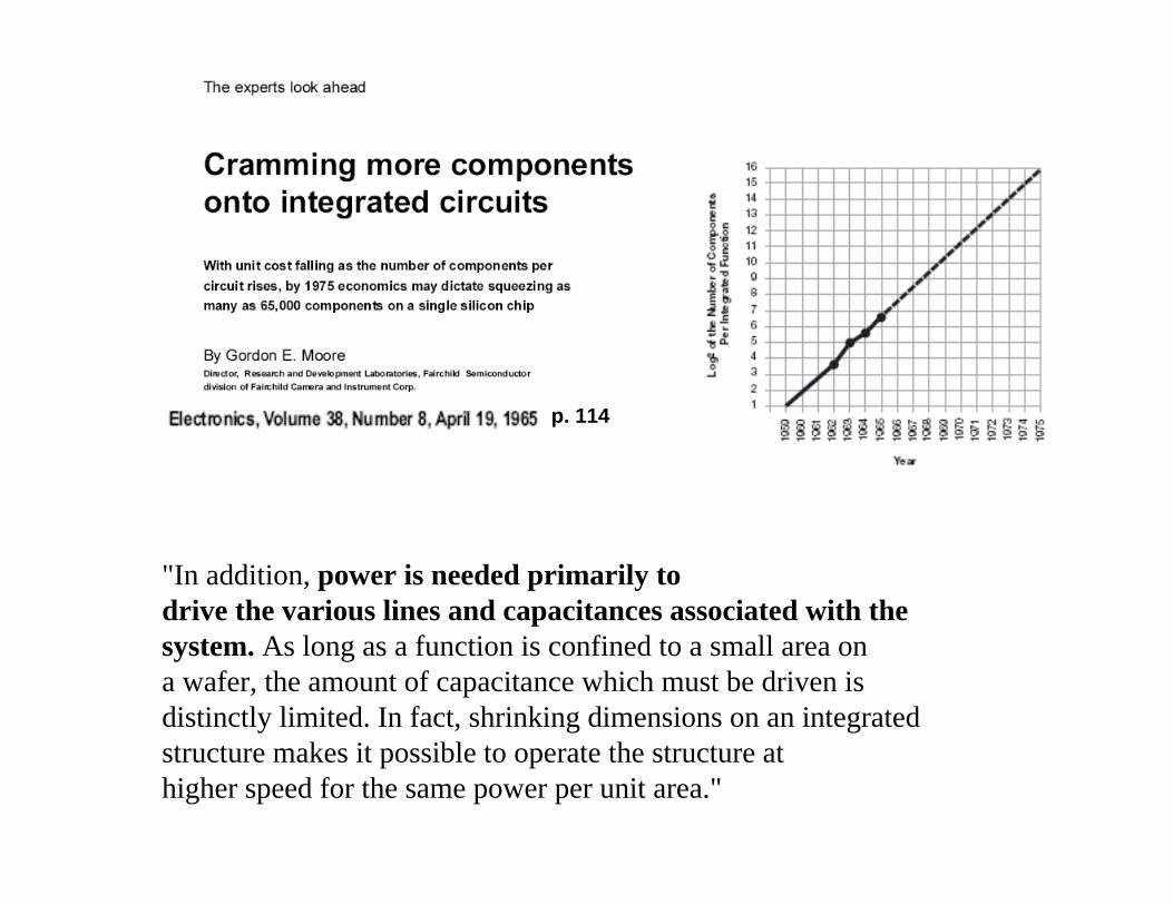
"In addition, power is needed primarily todrive the various lines and capacitances associated with thesystem. As long as a function is confined to a small area ona wafer, the amount of capacitance which must be driven isdistinctly limited. In fact, shrinking dimensions on an integratedstructure makes it possible to operate the structure athigher speed for the same power per unit area."
p. 114

l
Repeater Repeater Repeaterl l
a
RC time = (clock period) /2π
2R,Resistanceal
ρ=
lorεε≈Ce,Capacitanc
2
2
2 RC timeRC ⎟
⎠⎞
⎜⎝⎛ρεε=ρεε≈≡
al
al
oror
cm102F/cm102sec10
2periodclock
612
10
o Ω××≈
ρεπε=⎟
⎠⎞
⎜⎝⎛
−−
−
ral
4800≈⎟⎠⎞
⎜⎝⎛≡
alaspect
ratio of wire

<V2> = 4kT R ∆f
Vsignal = 0.56 milli-Volts
Ω=
Ω××=
ρ=⎟
⎠⎞
⎜⎝⎛ρ=ρ=
−
200045
1024800
4800R,Resistance
6
2
nmcm
aal
aal
⎟⎠⎞
⎜⎝⎛εε=εε≈
alal rr ooCe,Capacitanc
4800≈⎟⎠⎞
⎜⎝⎛≡
alaspect
ratio of wire
<I2> = 4(kT/R) ∆f
Isignal = 0.25 µAmps
C = εr εo a × 4800C ≈ 7 femto-Farads

Cq
qkTV
CkTV
RCRkTV
fRkTV
noise
noise
noise
noise
×=
=
=
∆=
4
4
14
4
2
2
2
2
What about very short wires?
Johnson Noise:
,4Cq
qkT
≈If
then the signals could be large enough to be efficiently amplified.
≡≤kTqC
2If The Coulomb
Blockade Capacitance.
For wires less than 1µm, a conventional transistor amplifier configuration may be adequate.
≈10 atto-Farads,

nano-transformerνh
~1eV
A low-voltage technology, or an impedance matching device,needs to be invented/discovered at the Nano-scale:
transistor amplifier with steeper sub-threshold slope photo-diode
+ ++
-
+VG
MEM's switch
Cryo-ElectronicskT/q~q/C
Cu
Cu
solid electrolyte
Electro-Chemical Switch
giant magneto-resistancespintronics
+

An amplifying transistor as a voltage matching device:Small voltage inLarge voltage out
in
outAmplification of weak signals has an energy cost!Amplification of weak signals has a speed penalty!
lnI
VgGate Voltage
Cur
rent
steep
ersu
b-th
resh
old
slope
correlated electron motion?
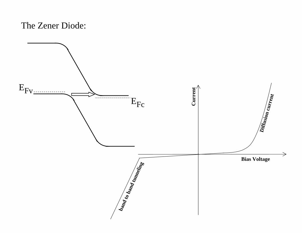
The Zener Diode:
EFc
EFv
band
to b
and
tunn
elin
g
Bias Voltage
Diff
usio
n cu
rren
t
Cur
rent

EF
band
to b
and
tunn
elin
g
Bias Voltage
Diff
usio
n cu
rren
t
Sharp Step
Cur
rent
The Esaki Diode:

The Backward Diode as a Switch:
EFc
EFv
band
to b
and
tunn
elin
g
Bias Voltage
Diff
usio
n cu
rren
t
Cur
rent
Sharp Step
The Backward Diode:These have been routinely made in Ge homo-junctions,since the 1960's.

The sub-threshold slope for tunneling depends
on the steepness of the band-edges:
The Backward Diode as a Switch:


I:
Steepness,
Low Operating Voltage
II:
On/Off Ratio
>105
III:
On-State Current Drive Capability,
mA/µm
or better: mS/µm
With tunneling alone, you can pick any
two out of the three above,
but you can't get all three!

Engineer Bands to Move Together
EngineeredUn-Engineered

Consider Thermal Vibrations
kx
ky
kz
xxε
kx
ky
kz
xyε
Uniaxial Strain
Shear Strain
Silicon Germanium
kx
ky
kz
kx
ky
kz
solid electrolyte
Cu
Cu
-
+VG1nm
Electro-Chemically Driven Metallic Switch:

nano-transformerνh
~1eV
A low-voltage technology, or an impedance matching device,needs to be invented/discovered at the Nano-scale:
transistor amplifier with steeper sub-threshold slope photo-diode
+ ++
-
+VG
MEM's switch
Cryo-ElectronicskT/q~q/C
Cu
Cu
solid electrolyte
Electro-Chemical Switch
giant magneto-resistancespintronics
+

That was Electrical Communication.
For longer distances,
Optical Communication is needed;How efficient can that be?
How many photons are needed?
This is mainly determined by the photodetectors.

Two-Dimensional Thin Film Photonic Crystals
Si/SiO2 SOI
SiO2
SiO2
Si
Si→1µm SOI
Cross-Section:
Luxtera, Inc.
Approved for Public Release
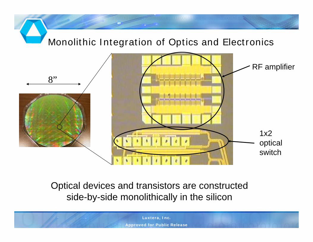
Monolithic Integration of Optics and Electronics
RF amplifier
1x2 optical switch
8”
Optical devices and transistors are constructed side-by-side monolithically in the silicon

Luxtera, Inc.
Approved for Public Release
CMOS Optical Modulator Performance
10G Eye
10G
Rolloff >20GHz

Blazar LUX5010Multirate 4x10G Optical Active Cable
Typical Applications•InfiniBand Connectivity SDR/DDR/QDR •10/40 Gigabit Ethernet •2 / 4 / 8 / 10 Gbps Fibre Channel •Proprietary Cluster Interconnect •Ethernet Local Area Network (LAN) •Storage Area Network (SAN) •2.5G / 5G PCI-Express Extension •Storage Arrays •Optical Backplanes •Rack-to-Rack, Shelf-to-Shelf Interconnect •Test Equipment

The problem is that optical communicationsAs it is currently practiced uses
>10,000 photons/bit of information communicated
This is mainly determined by the photodetectors.
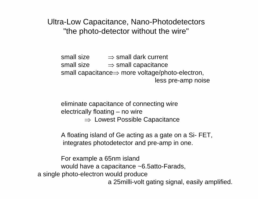
Ultra-Low Capacitance, Nano-Photodetectors"the photo-detector without the wire"
small size ⇒ small dark currentsmall size ⇒ small capacitancesmall capacitance⇒ more voltage/photo-electron,
less pre-amp noise
eliminate capacitance of connecting wireelectrically floating – no wire
⇒ Lowest Possible Capacitance
A floating island of Ge acting as a gate on a Si- FET,integrates photodetector and pre-amp in one.
For example a 65nm island would have a capacitance ~6.5atto-Farads,
a single photo-electron would produce a 25milli-volt gating signal, easily amplified.

Source Drain
SiO2
Silicon
FloatingGe island
n-Si
h+h+
e- e-
This is one of many types of photo-transistors!
Photons modulate depletion width
Photo-hetero-JFET concept:

p-Ge
n-Si
e–e–
e–e–
h+h+h+h+
Design Principle: Transistor with a Floating Gate
• Excess photo-holes attract electrons in the Silicon and change its conductance
• Open Ge/Si junction gets forward biased by an amount dependant on the light intensity
VF

SiO2
Silicon
Drain
Source
n-Si n-Si
Ge islandn-Si channel
Reflectors integrated with SOI waveguides to create a transverse cavity
incident light

The problem is that optical communicationsAs it is currently practiced uses
>10,000 photons/bit of information communicated
If the photodetector is small enough, and preamp is sensitive enough, we can anticipate getting this down to:
~15 photons/bit of information communicated
For a ~103 times improvement

"In addition, power is needed primarily todrive the various lines and capacitances associated with thesystem. As long as a function is confined to a small area ona wafer, the amount of capacitance which must be driven isdistinctly limited. In fact, shrinking dimensions on an integratedstructure makes it possible to operate the structure athigher speed for the same power per unit area."
p. 114

Conclusions:
1. Communications is a big bottleneck for reducing powering consumption in information processing.
2. The powering voltage for circuits is close to 1Volt,but it could be reduced to ~1milli-Volt,
for a 106 reduction in power.
3. Optical communications uses >10,000 photons/bit of information, but with more nanoscopic photodetectors this could be reduced to ~15photons/bit for a 103 reduction in power.
Charles Bennett, IBM
Reversible and Adiabatic Computing:
Energy/bit function <<kT

10µm
1µm
100nm
10nm
Moore's Law
1960 1980 2000
Crit
ical
D
imen
sion
2020 2040 2060Year
Tech
nolo
gy G
ap
Gates only
Gates including wires
107
105
102
1
0.1
104
106
10
108
103
Ene
rgy
per B
it fu
nctio
n (k
T)
The other , for energy per bit function
Shoorideh and Yablonovitch, UCLA 2006
Transistor Measurements by Robert Chau, Intel