logic circuits another look at floating point numbers common combinational logic circuits timing...
Post on 19-Dec-2015
222 views
TRANSCRIPT

Logic Circuits
• Another look at Floating Point Numbers
• Common Combinational Logic Circuits
• Timing
• Sequential Circuits
Note: Multiplication & Division in 2’s Complement is not as straight forward as addition and subtraction. For example, what happens if the multiplicand is negative?

Single Precision Floating Point Numbers
IEEE Standard
32 bit Single Precision Floating Point Numbers are stored as:
S EEEEEEEE FFFFFFFFFFFFFFFFFFFFFFF S: Sign – 1 bit E: Exponent – 8 bits F: Fraction – 23 bits
The value V:• If E=255 and F is nonzero, then V= NaN ("Not a Number") • If E=255 and F is zero and S is 1, then V= - Infinity • If E=255 and F is zero and S is 0, then V= Infinity • If 0<E<255 then V= (-1)**S * 2 ** (E-127) * (1.F) (exponent range = -127 to +128)• If E=0 and F is nonzero, then V= (-1)**S * 2 ** (-126) * (0.F) ("unnormalized" values”) • If E=0 and F is zero and S is 1, then V= - 0 • If E=0 and F is zero and S is 0, then V = 0
Note: 255 decimal = 11111111 in binary (8 bits)

FP Examples

Double Precision Floating Point Numbers
IEEE Standard
64 bit Double Precision Floating Point Numbers are stored as:
S EEEEEEEEEEE FFFFFFFFFFFFFFFFFFFFFFFFFFFFFFFFFFFFFFFFFFFFFFFFFFFF S: Sign – 1 bit E: Exponent – 11 bits F: Fraction – 52 bits
The value V:• If E=2047 and F is nonzero, then V= NaN ("Not a Number") • If E=2047 and F is zero and S is 1, then V= - Infinity • If E=2047 and F is zero and S is 0, then V= Infinity • If 0<E<2047 then V= (-1)**S * 2 ** (E-1023) * (1.F) (exponent range = -1023 to +1024)• If E=0 and F is nonzero, then V= (-1)**S * 2 ** (-1022) * (0.F) ("unnormalized" values) • If E=0 and F is zero and S is 1, then V= - 0 • If E=0 and F is zero and S is 0, then V= 0 Note: 2047 decimal = 11111111111 in binary (11 bits)

32 bit 2’s Complement Integer Numbers
All the Integers from -2,147,483,648 to + 2,147,483,647,
i.e. - 2 Gig to + 2 Gig-1

32 bit FP Numbers

“Density” of 32 bit FP Numbers
Note: ONLY 232 FP numbers are representable
There are only 232 distinct combinations of bits in 32 bits !

The Added Denormalized FP Numbers

Basic Logic gates
Note: NAND and NOR gates are “universal” gates, i.e. AND, OR, and NOT gates can all be created by either NAND or NOR gates.
NAND
NOR

DeMorgan’s Theorem/Law
• (NOT A) and (NOT B) = NOT (A or B)
• (NOT A) or (NOT B) = NOT (A and B)
Prove DeMorgan’s with truth tables:
A or B = NOT( (NOT A) and (NOT B) )
NOT (A or B) = (NOT A) and (NOT B)

Decoder
For N inputs, there are 2N outputs.
Any and all input combinations result in exactly one “true” output.

Multiplexor (MUX)
The output (OUT) is that input (A, B, C, or D) specified by the selector S.
Circuit Symbol

Full Adder
Full Adder Truth Table:

Full Adder Implementation

Program Logic Array
May be programmable
The input “and” gates provide all 2N combinations (minterms) of the N inputs.
The outputs (4 here) are the chosen “or” s of the minterms.
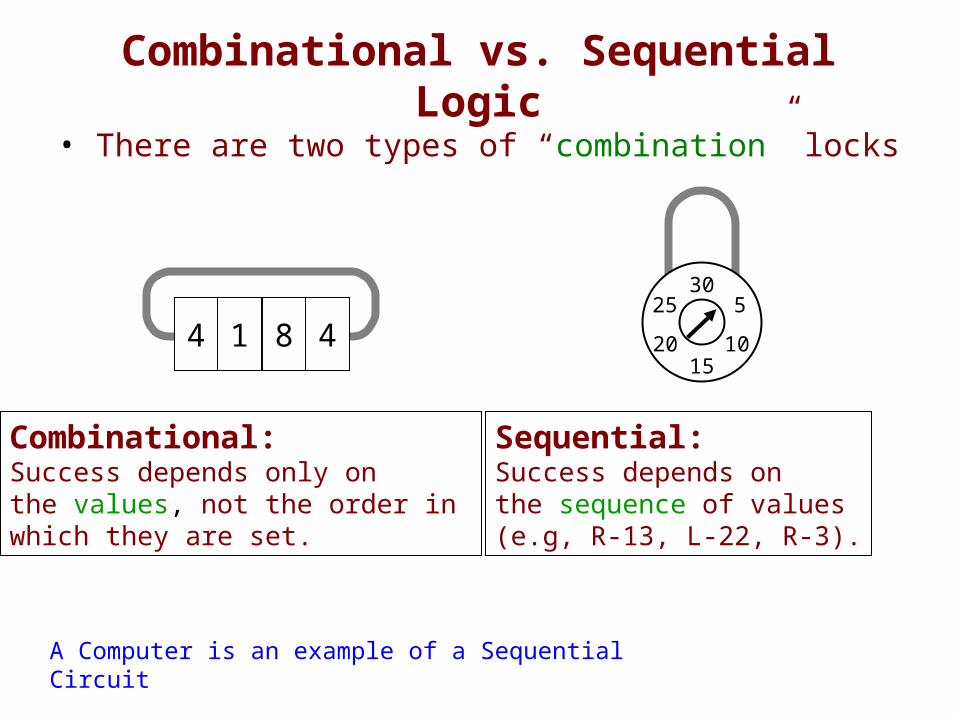
Combinational vs. Sequential Logic
• There are two types of “combination” locks
4 1 8 4
30
15
5
1020
25
Combinational:Success depends only onthe values, not the order in which they are set.
Sequential:Success depends onthe sequence of values(e.g, R-13, L-22, R-3).
A Computer is an example of a Sequential Circuit

Flip-Flop – 1 bit Storage
On the rising edge of the C input, the input to D is stored in the flip-flop, and can be read on output Q. It does not change until the next rising edge of the C input causes the new input on D to replace the value of Q.

Timing Diagram ConventionsTiming Diagram Conventions

Flip-Flop – 1 bit Storage
On the rising edge of the C input, the input to D is stored in the flip-flop, and can be read on output Q. It does not change until the next rising edge of the C input causes the new input on D to replace the value of Q.
Flip Flop Behavior:

Register – 8 bit Storage
An n-bit register is made up of n flip flops.
The n D inputs are “latched” into the register when the CLK signal goes positive.
When the /OE (output enable) input is a logic 0, the register Q outputs can be read.

As time permits
• Do division and more multiplication in 2’s complement.