loading mixity on the interfacial failure mode in lead ... papers/gao - astm - load... · feng...
TRANSCRIPT
Journal of ASTM International, Vol. 7, No. 5Paper ID JAI103021
Available online at www.astm.org
Feng Gao,1 Jianping Jing,2 Frank Z. Liang,3 Richard L. Williams,3 and Jianmin Qu4
Loading Mixity on the Interfacial Failure Mode in Lead-FreeSolder Joint
ABSTRACT: In this paper, single solder joints �SSJs� were subjected to moderate speed loading �5 mm/s�in different directions, from pure tensile mixity mode to pure shear. Fracture surfaces from different loadingdirections were examined both experimentally and numerically. The intermetallic compound �IMC� isformed between the solder alloy and the Cu pad, and the failure typically occurs at or near the solder/IMC/Cu interfaces of the board side. Pure tensile loading typically leads to interfacial fracture along theIMC/Cu interface. Mixity mode loading usually results in a mixture of interfacial and cohesive failure withdamage propagating in a zigzag fashion between the solder/IMC interface and the solder alloy. Loadingwith higher shear component tends to result in more cohesive failure of the solder alloy near the solder/IMCinterface. Under pure shear loading, failure is almost always cohesive within the solder alloy near thesolder/IMC interface.
KEYWORDS: lead-free solder, single solder joint, damage propagation, plastic deformation,interface, finite element analysis
Introduction
Due to the stiffer and more brittle characteristics of lead-free solder alloys, the solder joints of portableelectronic products are prone to drop and impact damage �1–6�. This is further compounded by packagingminiaturization, which reduces the amount of solder material available to absorb shock energy. It has beenfound that when a portable device drops on the floor, the local strain rate within a solder joint may varybetween 1 and 1000 s−1, depending on the drop height, orientation, and the properties of the floor surface�7�. The failure behavior of solder joints subjected to high strain rates has been studied extensively �8–12�.The tests are typically the ball grid array �BGA� component drop/impact tests at the board level, while thefailure usually initiates at the solder joint level. Thus understanding the failure process of a single solderjoint �SSJ� may lead to a more detailed damage mechanism. In the meantime, the high-speed pull andshear impact tests have also been utilized to evaluate the failure mode of the solder joints �13–17�. Inreality, solder ball interconnections may be subjected to the combined tensile, shear, and peeling stresses.Therefore a realistic assessment of solder ball integrity should consider the loading components simulta-neously. However, there is very little study on the failure behavior of solder joint under different loadingmixities at an intermediate strain rate range between 1 and 100 s−1. The larger loading mixity indicates agreater shear component but a less normal component. Therefore, there has been a critical need to under-stand failure modes and mechanism of a SSJ subjected to dynamic loading mixity at intermediate strainrate.
In this study we report some results regarding failure mode under a moderate strain rate and how thefailure mode changes under different combinations of normal and shear loading. The SSJs were subjectedto velocity controlled loading. The optical microscopy on fracture surface was conducted to verify thefailure mode. To interpret the experimental observations, the finite element analysis was performed tounderstand the failure mechanism during the dynamic loading process.
Manuscript received February 2, 2010; accepted for publication April 21, 2010; published online June 2010.1 George W. Woodruff School of Mechanical Engineering, Georgia Institute of Technology, Atlanta, GA 30332-0405 and McCor-mick School of Engineering and Applied Science, Northwestern Univ., Evanston, IL 60208, e-mail: [email protected] The State Key Laboratory of Mechanical System and Vibration, Shanghai JiaoTong Univ., Shanghai 200000, China.3 Intel Corporation, Hillsboro, OR 97124.4 George W. Woodruff School of Mechanical Engineering, Georgia Institute of Technology, Atlanta, GA 30332-0405 and McCor-
mick School of Engineering and Applied Science, Northwestern Univ., Evanston, IL 60208.Copyright © 2010 by ASTM International, 100 Barr Harbor Drive, PO Box C700, West Conshohocken, PA 19428-2959.
2 JOURNAL OF ASTM INTERNATIONAL
Experimental Procedures
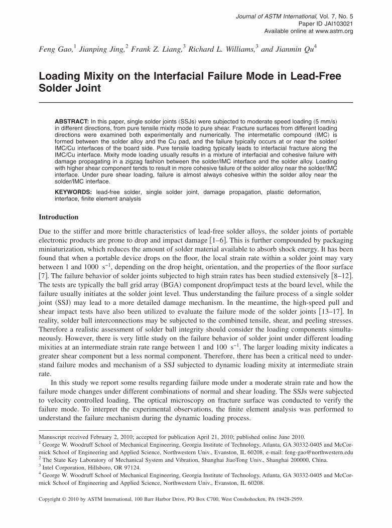
The SSJ samples used in this study were laser-cut from a BGA package assembled on a printed circuitboard �PCB�. A schematic of the finished SSJ is shown in Fig. 1�a�. The commercial Sn-4.0Ag-0.5Cu�SAC405� solder alloy was used with the SSJ failure to occur along the PCB interfaces. This was accom-plished by designing the BGA package–solder ball interface area greater than the solder joint–PCB inter-face area, commonly referred to as the solder joint aspect ratio. The SSJ samples are loaded using ahigh-speed loading frame equipped with a specially design test apparatus. Samples can be gripped indifferent orientations so that the loading angle � between the loading direction and the PCB surface canvary with 0° corresponding to pure tension and 90° corresponding to pure shear.
Another unique feature of the test apparatus is that the load is not applied to the SSJ sample until thegrip has reached the desired speed. This removes the inertia of the load frame and applies a true impactload to the SSJ sample with known velocity.
FIG. 1—The SSJ testing: (a) The schematic diagram of the SSJ; (b) experimental force-displacementcurves versus loading mixity.
In this study, tests were conducted under four loading angles of 0°, 30°, 60°, and 90° to investigate the

GAO ET AL. ON LOADING MIXITY ON INTERFACIAL FAILURE MODE 3
effect of loading mixity. The board substrate of the SSJ was fixed, while the substrate at the package sidewas subjected to the velocity loading. The grip was set to move at 5 mm/s. The reaction force measuredby the load sensor attached to the grip was recorded every 2�10−4 s. The corresponding grip displace-ment was also recorded to obtain the force versus time or force versus displacement curve. The cross-sectional optical microcopy was conducted on the SSJ samples both before and after the dynamic test.
Results and Discussion
Figure 1�b� illustrates the measured force-displacement curves due to different loading mixity at 5 mm/s.Basically, the peak force continues to decrease with the larger loading mixity, namely, the greater shearcomponent. On the contrary, the time of the peak force occurrence increases with the larger loading mixity.In addition, the full failure displacement for shear test is much larger than that of pure tensile test. Theseresults indicate that the different failure mode may take place under different loading mixity, which will bestressed in detail below based on the fracture surface observations.
Figure 2�a� shows the microstructure of a SSJ before testing. The intermetallic compound �IMC� wasformed at both PCB board and package sides, acting as the metallurgical interconnection. The non-homogeneous microstructure of solder alloy consists of �-Sn, ��-Sn+Ag3Sn� eutectic, and ��-Sn
FIG. 2—The microstructure of SSJ: (a) Optical micrograph; (b) the corresponding polarized image.
+Ag3Sn+Cu6Sn5� eutectic phases. Large-needle-shaped Ag3Sn particles are also observed, which is at-

4 JOURNAL OF ASTM INTERNATIONAL
FIG. 3—Failure occurs along the IMC/Cu interface at the board side at 0° loading: (a) Solder joint at
package side; (b) close-up of the fracture interface; and (c) residue Cu pad at board side.
GAO ET AL. ON LOADING MIXITY ON INTERFACIAL FAILURE MODE 5
tributed to the high initial Ag content in SAC405 and the solidification process �18�. Figure 2�b� is apolarized image showing that there are only a few grains in a SSJ. The different contrast of these grainsrepresents different grain orientations. Such high non-homogeneous grain structure will partially affect thematerial property of the small size lead-free solder ball.
In order to investigate the effect of loading mixity, four different loading directions were used, that is,0° �pure tensile�, 30°, 60°, and 90° �pure shear�. It is found that the majority of SSJ samples failed at theinterfaces of the board side. Figures 3–6 illustrate the failure behavior of the SSJ samples under theloading rate of 5 mm/s at different loading angles.
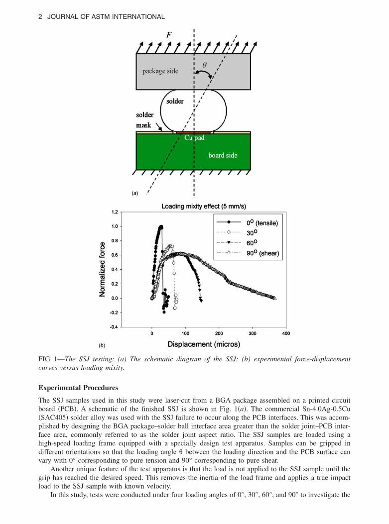
It is seen from Fig. 3�a� that under pure tensile loading, the damage develops along the IMC/Cuinterface of the board side. Almost all the IMC is attached with the solder ball, while only little IMCresidue is probed on the Cu pad, as shown in Fig. 3�b� and 3�c�. Thus a brittle interfacial fracture along theIMC/Cu interface of the board side is suggested. Figure 4 shows a SSJ sample failed under a loading angleof 30°. Again, failure occurs at the board side; see Fig. 4�a�. However, the fracture surface is no longer atthe IMC/Cu interface. Its zigzag path alternates between the solder alloy and the solder/IMC interface, asillustrated in Fig. 4�b�. Under a higher loading angle of 60°, the facture path shows the similar zigzag formwith more cohesive failure within the solder alloy; see Fig. 5�a� and 5�b�. Under pure shear loading at 90°,
FIG. 4—Failure occurs along the path of (solder / IMC�solder matrix) at board side under the loadingmixity of 30°: (a) Solder joint at package side; (b) residue Cu pad at board side.
failure occurs almost entirely within the solder alloy near the solder/IMC interface, as shown in Fig. 6�a�

6 JOURNAL OF ASTM INTERNATIONAL
and 6�b�. In addition, Figs. 4�a�, 5�a�, and 6�a� also show the plastic deformation behavior of the solderball due to the shear component of the angular loading. The higher the loading angle, the more severe theshear deformation.
In summary, under the loading speed of 5 mm/s, pure normal tension leads to a brittle interfacialfailure of the IMC/Cu pad interface. Higher loading angle, which corresponds to a larger shear component,leads to a more cohesive failure within the solder alloys, while pure shear loading results in almost entirelycohesive failure. At the high drop/impact loading rate, the failure of lead-free solder joint is usually brittleand occurs at the IMC/substrate interface regardless of the loading mixity �e.g., tension or shear��1–4,8–10�. Our experimental results show that at the moderate strain rate as the solder joint studiedherein, the loading mode will be sensitive to the loading mixity.
To better understand and interpret the experimental observations discussed above, the testing underdifferent loading mixities was simulated using the finite element method. The simulation was conductedusing the commercial software ABAQUS®. The three-dimanional �3D� geometry of a typical SSJ is shownin Fig. 7�a�. A 3D finite element model is then constructed for a SSJ. The following components areincluded in this model: Substrates at package and board sides, Ni finish at package side, Cu pad at boardside, SAC405 lead-free solder ball, solder mask, and IMC layers between solder and Cu pad at board sides.
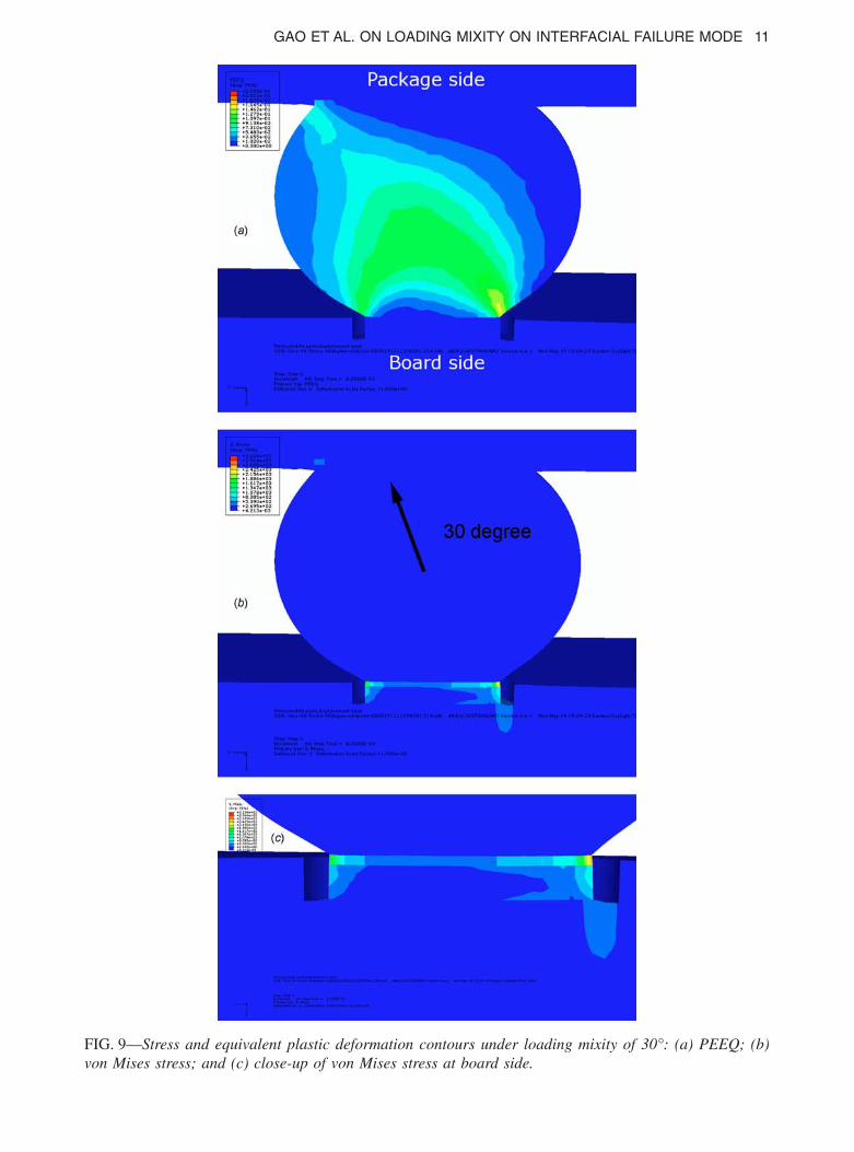
FIG. 5—Failure occurs along the path of (solder / IMC�solder matrix) at board side under the loadingmixity of 60°: (a) Solder joint at package side; (b) residue Cu pad at board side.
Figure 7�b� depicts a close-up configuration of the interfaces at both package and board sides. All relevant

GAO ET AL. ON LOADING MIXITY ON INTERFACIAL FAILURE MODE 7
geometric dimensions and materials properties are listed in Tables 1–3. The intermetallic compound isregarded as Cu6Sn5 at board side. Their properties are determined based on the first-principles calculation�19�. In particular, the SAC405 solder is modeled as elastic-plastic using classic metal plasticity law, whichis extracted inversely by fitting the experimental force-displacement curve. The results are illustrated inTable 4. To simulate a dynamic loading, the bottom surface of the finite element model is constrained inx-, y-, and z-directions, which mimic the situation where the bottom of the sample is glued to a rigidsubstrate. A velocity of 5 mm/s is prescribed for all the nodes on the top surface of the finite elementmodel.
In order to reveal the plastic deformation or stress fields clearly, cross-sectional illustrations arepresented below. The stress field is expected to indicate the potential site for the damage initiation, whilethe equivalent plastic strain �PEEQ� at the solder alloy is employed to show the possible damage propa-gation path qualitatively. The corresponding simulation results are presented in Figs. 8–11.
Figure 8�a� and 8�b� shows the plastic deformation and von Mises-stress contours under pure tensileloading �0°�, respectively. It can be seen that the maximum stress concentration is formed at the edge ofsolder/IMC/Cu pad interfaces of the board side. Figure 8�c� illustrates the close-up of the von Mises-stressfield at the interface area of the board side. At the package side, no severe stress concentration is observed.
FIG. 6—Failure occurs along the solder ball near the solder/IMC interface of board side under the pureshear loading (90°): (a) Solder joint at package side; (b) residue Cu pad at board side.
This indicates that the solder/IMC/Cu interfaces at the board side is the dangerous site for the damage

8 JOURNAL OF ASTM INTERNATIONAL
initiation, which is consistent with the experimental observations. The maximum plastic deformation ismainly located at the edge of the interface between the solder alloy and the IMC layer and expandstowards the solder alloy. Interestingly, at the board side, the solder alloy adjacent to the IMC layer does notsuffer a remarkable plastic deformation, as shown in Fig. 8�a�. Since the plastic deformation in theadjacent ductile layer �SAC405 lead-free solder alloy� has remarkable toughening effect on the interfacefracture �2,13�, it can be concluded that the SSJ is more susceptible to the brittle interfacial fracture alongthe IMC/Cu interface under high pure tensile loading.
Under the loading mixities of 30° and 60°, the maximum stress concentration still exists at the edge ofsolder/IMC/Cu interfaces. However, due to the shear stresses, the asymmetry stress contours are formed,as shown in Figs. 9�b� and 10�b�. In Figs. 9�b� and 10�b�, the maximum stress concentration is located atthe right edge of the board side interfaces, which corresponds to the damage initiation site. In addition, theshear stress also leads to an asymmetry plastic deformation contour of the solder alloy, as shown in Figs.9�a� and 10�a�. A relatively severe plastic deformation at the left edge of the package side is also formed.The maximum plastic deformation occurs at the right edge of the board side, which may also engender thedamage initiation at that location.
It is interesting to notice that the plastic deformation of the solder alloy adjacent to the IMC layer is
FIG. 7—Numerical simulation model of SSJ: (a) 3D geometry of a SSJ; (b) close-up of the interfacesconfiguration at both package and board sides.
also altered. That is, the plastic deformation area of solder ball adjacent to solder/IMC interface tends to be

GAO ET AL. ON LOADING MIXITY ON INTERFACIAL FAILURE MODE 9
enhanced with loading angle �or larger shear component�. Obviously, this will make the damage propa-gation shift up to the solder/IMC interface or even the solder alloys. Due to the different magnitudes of theplastic deformation along the solder/IMC interface, as shown in Figs. 9�a� and 10�a�, zigzag damagepropagation along the path �solder/IMC interface+solder matrix� may occur. This simulation result isconsistent with the microstructure observations shown in Figs. 4�b� and 5�b�. Under the pure shear loading�90°�, as shown in Fig. 11�a�, the maximum plastic deformation lies on the solder ball area adjacent toIMC layer, which is more effective to release the solder/IMC interfacial energy by the solder alloy. Thiswill result in an entire cohesive failure within the solder alloys, which is also consistent with the experi-mental results shown in Fig. 6�b�.
Conclusions
The damage behavior of a SSJ subjected to different loading mixities at 5 mm/s rate is investigated in thiswork. It is found that the failure typically occurs at or near the solder/IMC/Cu interfaces on the board side.Simulation result also shows that the maximum stress concentration occurs at the solder/IMC/Cu interfaceson the board side, which corresponds to the dangerous sites for the damage initiation. Pure tensile loadingtypically leads to interfacial fracture along the IMC/Cu interface. Mixed mode loading usually results in amixture of interfacial and cohesive failure with damage propagating in a zigzag fashion between thesolder/IMC interface and the solder alloy. Loading with higher shear component tends to result in morecohesive failure of the solder alloy near the solder/IMC interface. Under pure shear loading, failure isalmost always cohesive within the solder ball near the solder/IMC interface. The failure mode transition isattributed to the plastic deformation alteration of solder alloy adjacent to the IMC layer on the board side.
TABLE 1—Dimensions of SSJ specimen.
PCB Cu pad interface diameter ��m� 350
Substrate pad interface diameter ��m� 450
Solder ball diameter ��m� 550
Solder joint height ��m� 330
Substrate/PCB �width�depth� ��m� 1400�1120
TABLE 2—Isotropic material parameters.
Solder �GPa� Copper �GPa� SM �GPa� IMC �GPa��19�
E 53 117 24 119
v 0.3425 0.34 0.4 0.29
TABLE 3—Anisotropic material parameters.
E1,v1�GPa,/�
E2,v2�GPa,/�
E3,v3�GPa,/�
G12�GPa�
G13�GPa�
G23�GPa�
PCB 22, 0.28 22,0.28 4.8,0.18 8 4 4
Substrate 21,0.3 21,0.3 6,0.2 8 4 4
TABLE 4—Elastic-plastic property of SAC405 solder alloy.
Flow stress �MPa� 26 60 80 120 150
Plastic strain 0 0.005 0.01 0.03 0.05

10 JOURNAL OF ASTM INTERNATIONAL
FIG. 8—Stress and equivalent plastic deformation (PEEQ) contours under pure tensile loading (0°): (a)PEEQ; (b) von Mises stress; and (c) close-up of von Mises stress at board side.
GAO ET AL. ON LOADING MIXITY ON INTERFACIAL FAILURE MODE 11
FIG. 9—Stress and equivalent plastic deformation contours under loading mixity of 30°: (a) PEEQ; (b)
von Mises stress; and (c) close-up of von Mises stress at board side.
12 JOURNAL OF ASTM INTERNATIONAL
FIG. 10—Stress and equivalent plastic deformation contours under loading mixity of 60°: (a) PEEQ; (b)
von Mises stress; and (c) close-up of von Mises stress at board side.
GAO ET AL. ON LOADING MIXITY ON INTERFACIAL FAILURE MODE 13
FIG. 11—Stress and equivalent plastic deformation contours under pure shear loading (90°): (a) PEEQ;(b) von Mises stress; (c) close-up of von Mises stress at board side.

14 JOURNAL OF ASTM INTERNATIONAL
Acknowledgments
The financial support from Intel Corporation is greatly acknowledged. Also the writers would like to thankMr. Carter Ralph for the sample preparation and test setup.
References
�1� Wong, E. H., Rajoo, R., Seah, S. K. W., Selvanayagam, C. S., van Driel, W. D., Caers, J. F. J. M.,Zhao, X. J., Owens, N., Tan, L. C., Leoni, M., Eu, P. L., Lai, Y.-S., and Yeh, C.-L., “CorrelationStudies for Component Level Ball Impact Shear Test and Board Level Drop Test,” Microelectron.Reliab., Vol. 48, 2008, pp. 1069–1078.
�2� Suh, D., Kim, D.-W., Liu, P. L., Kim, H., Weninger, J. A., Kumar, C. M., Prasad, A., Grimsley, B.W., and Tejada, H. B., “Effects of Ag Content on Fracture Resistance of Sn–Ag–Cu Lead-FreeSolders Under High-Strain Rate Conditions,” Mater. Sci. Eng., A, Vol. 460–461, 2007, pp. 595–603.
�3� Wong, E. H. and Mai, Y.-W., “Advances in the Drop-Impact Reliability of Solder Joints for MobileApplications,” Microelectron. Reliab., Vol. 49, 2009, pp. 139–149.
�4� Wong, E. H., Selvanayagam, C. S., Seah, S. K. W., van Driel, W. D., Caers, J. F. J. M., Zhao, X. J.,Owens, N., Tan, L. C., Frear, D. R., Leoni, M., Lai, Y.-S., and Yeh, C.-L., “Stress-Strain Character-istics of Tin-Based Solder Alloys for Drop-Impact Modeling,” J. Electron. Mater., Vol. 37, 2008, pp.829–836.
�5� Liu, Y. L., Gale, S., and Johnson, R. W., “Investigation of the Role of Void Formation at theCu-to-Intermetallic Interface on Aged Drop Test Performance,” IEEE Trans. Electron. Packag.Manuf., Vol. 30, 2007, pp. 63–73.
�6� Mattila, T. T., Marjamaki, P., and Kivilahti, J. K., “Reliability of CSP Interconnections Under Me-chanical Shock Loading Conditions,” IEEE Trans. Compon. Packag. Technol., Vol. 29, 2006, pp.787–795.
�7� Long, X., Dutta, I., Sarihan, V., and Frear, D. R., “Deformation Behavior of Sn-3.8Ag-0.7Cu Solderat Intermediate Strain Rates: Effect of Microstructure and Test Conditions,” J. Electron. Mater., Vol.37, 2008, pp. 189–200.
�8� Yeh, C.-L., Lai, Y.-S., and Kao, C.-L., “Evaluation of Board-Level Reliability of Electronic PackagesUnder Consecutive Drops,” Microelectron. Reliab., Vol. 46, 2006, pp. 1172–1182.
�9� Luan, J.-E., Tee, T. Y., Pek, E., Lim, C. T., and Zhong, Z. W., “Dynamic Responses and Solder JointReliability Under Board Level Drop Test,” Microelectron. Reliab., Vol. 47, 2008, pp. 450–460.
�10� Wong, E. H., Seah, S. K. W., and Shim, V. P. W., “A Review of Board Level Solder Joints for MobileApplications,” Microelectron. Reliab., Vol. 48, 2008, pp. 1747–1758.
�11� Li, J., Mattila, T. T., and Kivilahti, J. K., “Computational Assessment of the Effects of Temperatureon Wafer-Level Component Boards in Drop Tests,” IEEE Trans. Compon. Packag. Technol., Vol. 32,2009, pp. 38–43.
�12� Zaal, J. J. M., van Driel, W. D., Kessels, F. J. H. G., and Zhang, G. Q., “Correlating Drop ImpactSimulations with Drop Impact Testing Using High-Speed Camera Measurements,” J. Electron.Packag., Vol. 131, 2009, pp. 011007.
�13� Yeh, C.-L. and Lai, Y.-S., “Effect of Solder Alloy Constitutive Relationships on Impact Force Re-sponse of Package-Level Solder Joints Under Ball Impact Test,” J. Electron. Mater., Vol. 35, 2006,pp. 1892–1901.
�14� Lai, Y.-S., Yeh, C.-L., Chang, H.-C., and Kao, C.-L., “Characterizations of Ball Impact Responses ofWafer-Level Chip-Scale Packages,” J. Alloys Compd., Vol. 450, 2008, pp. 238–244.
�15� Morita, T., Kajiwara, R., Ueno, I., and Okabe, S., “New Method for Estimating Impact Strength ofSolder-Ball Bonded Interfaces in Semiconductor Packages,” Jpn. J. Appl. Phys., Vol. 47, 2008, pp.6566–6568.
�16� You, T., Kim, Y., Kim, J., Lee, J., Jung, B., Moon, J., and Choe, H., “Predicting the Drop Perfor-mance of Solder Joint by Evaluating the Elastic Strain Energy from High-Speed Ball Pull Tests,” J.Electron. Mater., Vol. 38, 2009, pp. 410–414.
�17� Liu, D.-S., Kuo, C.-Y., Hsu, C.-L., Shen, G.-S., Chen, Y.-R., and Lo, K.-C., “Failure Mode Analysis

GAO ET AL. ON LOADING MIXITY ON INTERFACIAL FAILURE MODE 15
of Lead-Free Solder Joints Under High Speed Impact Testing,” Mater. Sci. Eng., A, Vol. 494, 2008,pp. 196–202.
�18� Gao, F., Nishikawa, H., and Takemoto, T., “Intermetallics Evolution in Sn-3.5Ag Based Lead-FreeSolder Matrix on an OSP Cu Finish,” J. Electron. Mater., Vol. 36, 2007, pp. 1630–1634.
�19� Lee, N. T. S., Tan, V. B. C., and Lim, K. M., “First-Principle Calculations of Structural and Me-chanical Properties of Cu6Sn5,” Appl. Phys. Lett., Vol. 88, 2006, pp. 031913.