lncs 3659 - scalable hardware for sparse systems of linear … · 2017-08-25 · scalable hardware...
TRANSCRIPT

Scalable Hardware for Sparse Systems of LinearEquations, with Applications to Integer
Factorization
Willi Geiselmann1, Adi Shamir2, Rainer Steinwandt1,3, and Eran Tromer2
1 IAKS, Arbeitsgruppe Systemsicherheit, Prof. Dr. Th. Beth,Fakultat fur Informatik, Universitat Karlsruhe, 76131 Karlsruhe, Germany
{geiselma, steinwan}@ira.uka.de2 Department of Computer Science and Applied Mathematics,
Weizmann Institute of Science, Rehovot 76100, Israel{adi.shamir, eran.tromer}@weizmann.ac.il
3 On leave to Department of Mathematical Sciences,Florida Atlantic University, Boca Raton, FL 33431-0991, USA
Abstract. Motivated by the goal of factoring large integers using theNumber Field Sieve, several special-purpose hardware designs have beenrecently proposed for solving large sparse systems of linear equationsover finite fields using Wiedemann’s algorithm. However, in the contextof factoring large (1024-bit) integers, these proposals were marginallypractical due to the complexity of a wafer-scale design, or alternativelythe difficulty of connecting smaller chips by a huge number of extremelyfast interconnects.
In this paper we suggest a new special-purpose hardware device forthe (block) Wiedemann algorithm, based on a pipelined systolic archi-tecture reminiscent of the TWIRL device. The new architecture offerssimpler chip layout and interconnections, improved efficiency, reducedcost, easy testability and greater flexibility in using the same hardwareto solve sparse problems of widely varying sizes and densities. Our analy-sis indicates that standard fab technologies can be used in practice tocarry out the linear algebra step of factoring 1024-bit RSA keys.
As part of our design but also of independent interest, we describe anew error-detection scheme adaptable to any implementation of Wiede-mann’s algorithm. The new scheme can be used to detect computationalerrors with probability arbitrarily close to 1 and at negligible cost.
Keywords: Factorization, number field sieve, sparse systems of linearequations.
1 Introduction
In recent years, various special-purpose hardware implementations of the Num-ber Field Sieve (NFS) algorithm have been proposed for factoring large (e.g.,1024-bit) integers. These devices address two two critical steps of the NFS: thesieving step [1,2,3,4,5,6,7] and the linear algebra step [8,9,10,11].
J.R. Rao and B. Sunar (Eds.): CHES 2005, LNCS 3659, pp. 131–146, 2005.c© International Association for Cryptologic Research 2005
132 W. Geiselmann et al.
This work focuses on the linear-algebra step of the NFS. While the cost ofthis step seems to have been reduced to below that of the sieving step (for 1024-bit composites) by the most recent proposals [10,11], practically these designsare not fully satisfactory: they require (various combinations of) extremely largechips, non-local wiring and high-bandwidth chip interconnects, and thus posesignificant technological hurdles.
Below we describe a new systolic design for the NFS linear algebra step, andspecifically for the matrix-by-vector multiplications which dominate the cost ofthe Wiedemann algorithm. This design is both more efficient and more realisticthan previous ones. In its simplest form, it consists of a one dimensional chainof identical chips with purely local interconnects, which from a practical stand-point makes it an attractive alternative to previous wafer-scale mesh proposals.For higher efficiency it can be generalized to a two-dimensional array of chips,but unlike previous proposals, this device has standard chip sizes, purely localinterconnects, and can use standard DRAM chips for some of its components.In addition, the new design is highly scalable: there is no need to commit toparticular problem sizes and densities during the chip design phase, and thereis no need to limit the problem size to what can be handled by a single wafer.Since a single chip design of small fixed size can handle a wide range of sparsematrix problems (some of which may be related to partial differential equationsrather than cryptography), the new architecture can have additional applica-tions, greatly reduced technological uncertainties, and lower initial NRE cost.
Unlike previous routing based proposals, whose complex data flows requiredsimulation of the whole device and were not provably correct, the present devicehas a simple and deterministic data flow, so that each unit can be simulated inde-pendently. This facilitates the simulation and actual construction of meaningfulproof-of-concept sub-devices.
We have evaluated the cost of this device for a specific choice of matrixparameters, which is considered a conservative estimate for the matrix size infactoring 1024-bit integers using NFS. The estimated area×time cost is 6.5 lowerthan the best previous proposal; the concrete cost estimate is 0.4M US$×year(i.e., excluding non-recurring R&D costs, US$ 0.4M buys enough hardware toobtain a throughput of one solved linear algebra instance per year).
The present design adapts efficiently and naturally to operations over anyfinite field GF(q), since it does not depend on the in-transit pairwise cancellationof values in GF(2). In particular, it can support the new algorithm of Frey [12,13].In fact, it can be used with minor modifications over any ground field, such asthe rationals or complex numbers.
Section 2 recalls basic facts about Wiedemann’s algorithm and its context inthe NFS. Section 3 describes the new hardware architecture. In any large-scalecomputation the handling of faults is crucial; Section 4 presents a particularlyefficient error detection scheme, which can also be adapted to other implemen-tations of block Wiedemann. Section 5 gives a preliminary cost analysis for pa-rameters currently considered as plausible for 1024-bit numbers, and comparesit to previous proposals.

Scalable Hardware for Sparse Systems of Linear Equations 133
2 Preliminaries
For an introduction to the NFS algorithm we refer to [14], and for a detailedaccount to [15]. Here it is sufficient to keep in mind that the overall running timeof the NFS algorithm is dominated by the sieving step and the linear algebrastep. In this paper we exclusively consider the linear algebra step, defined asfollows. We are given a D × D matrix A over GF(2), whose columns correspondto relations found in the preceding sieving step (after some pre-processing). Ourgoal is to find a few vectors in the kernel of A, i.e., several sets of relations thatsum to the zero vector. This matrix is large but sparse, with a highly non-uniformdistribution of row densities. As in previously proposed devices [8,9,10,11], weemploy the block Wiedemann algorithm [16,17] for solving sparse systems oflinear equations. Basically, the block Wiedemann algorithm reduces the aboveto the problem of computing sequences of the form
Av, A2v, . . . , Atv (1)
for some v ∈ GF(2)D. Such a sequence can be computed by means of t matrix-by-vector multiplications, where the matrix A remains fixed and the vector varies.Overall, roughly 2D such multiplications are needed, divided into 2K chains,where K > 32 is the blocking factor. The resulting products are not explicitlyoutput after each multiplication; depending on the phase of Wiedemann’s algo-rithm, only their inner product with some fixed vectors or their (partial) sumsare needed.
Parameters for 1024-bit Composites. At present there is considerable un-certainty about the size and density of the matrix one would encounter in thefactorization of a 1024-bit composite, for several reasons: freedom in the choiceof the NFS parameters, freedom in the application of pre-processing to the ma-trix (e.g., to cancel out “large primes”), and lack of complete analysis of thisaspect of the NFS algorithm. For concreteness and ease of comparison, in thefollowing we shall assume the “large matrix” parameters from [9], namely a sizeof D × D for D ≈ 1010 and density of 100 entries per column. This leaves agenerous conservative margin compared to the smaller matrix expected to beproduced by TWIRL [4].
For the sake of concreteness, we propose a concrete instance of our architec-ture where various design parameters are chosen suitable for the above NFS pa-rameters. In the following, these concrete parameters are designated by angularbrackets (e.g., D 〈〈= 1010〉〉). Section 5 provides additional details and discussesthe cost of the device for these parameters.
3 The New Architecture
We shall unravel the architecture in several stages, where each stage generalizesthe former and (when appropriately parameterized) improves its efficiency.

134 W. Geiselmann et al.
3.1 Basic Scheme
The proposed hardware device is preloaded with a compressed representation ofthe sparse matrix A ∈ GF(2)D×D, as will be detailed below. For each multipli-cation chain, we load the input vector v and iteratively operate the device tocompute the vectors Av, A2v, . . . , Atv and output the appropriate sums or innerproducts.
We begin by describing an inefficient and highly simplified version of thedevice, to illustrate its high-level data flow.1 This simplified device consists ofD 〈〈= 1010〉〉 stations connected in a pipeline. The i-th station is in charge ofthe i-th matrix row, and contains a compressed representation of the 〈〈≈ 100〉〉non-zero entries in that row. It is also in charge of the i-th entry of the outputvector, and contains a corresponding accumulator W ′[i].
In each multiplication, the input vector v ∈ GF(2)D is fed into the top ofthe pipeline, and moves down as in a shift register. As the entries of v pass by,the i-th station looks at all vector entries vj passing through it, identifies theones corresponding to the non-zero matrix entries Ai,j in row i, and for thoseentries adds Ai,j · vj to its accumulator W ′[i]. Once the input vector has passedall stations in the pipeline, the accumulators W ′[·] contain the entries of theproduct vector Av. These can now be off-loaded and fed back to the top of thepipeline in order to compute the next multiplication.
The one-dimensional chain of stations can be split across several chips: eachchip contains one or more complete stations, and the connections between sta-tions may span chip boundary. Note that since communication is unidirectional,inter-chip I/O latency is not a concern (though we do need sufficient bandwidth;the amount of bandwidth needed will increase in the variants given below, andis taken into account in the cost analysis of Section 5).
3.2 Compressed Row Handling
Since the matrix A is extremely sparse, it is wasteful to dedicate a completestation for handling each row of A, as it will be idle most of the time. Thus, wepartition A into u 〈〈= 9600〉〉 horizontal stripes and assign each such stripe to asingle station (see Figure 1). The number of rows per station is µ ≈ D/u 〈〈= 220〉〉,and each station contains µ accumulators W ′[i] with i ranging over the set ofrow indices handled by the station.
Each station stores all the non-zero matrix entries in its stripe, and containsan accumulator for each row in the stripe. As before, the input vector v passesthrough all stations, but now there are just u of these (rather than D). Since theentries of v arrive one by one, each station implicitly handles a µ×D submatrixof A at each clock cycle.
1 This basic version is analogous to the electronic pipeline-of-adders version of TWIN-KLE [2], and many of the improvements described in the following have correspond-ing analogues in the TWIRL architecture [4].

Scalable Hardware for Sparse Systems of Linear Equations 135
Station 1
Station u
...
v
A
Fig. 1. Distributing theentries of A onto stations
proc. 1 v1+k(u-1)
proc. k vk+ku
. . .
. . .
. . .
. . .
station u
. . .
. . .
. . .
. . .
station 1
. . . proc. 1 v1
proc. k vk. . .
Fig. 2. Subdivision of a chip into stations andprocessors
3.3 Compressed Vector Transmission
For additional efficiency, we add parallelism to the vector transmission. Insteadof each station processing a single entry of v in each clock-cycle, we process v inchunks of k 〈〈= 32〉〉 consecutive entries.2 The inter-station pipeline is thickenedby a factor of k. The vector v now passes in chunks of k entries over an inter-station pipeline (in Figure 2 from right to left); in each clock cycle, each stationobtains such a chunk from the previous station (to its right), processes it andpasses it to the next station (to its left). The first (rightmost) station gets a newpart of the vector received from the outside. At each clock cycle, each stationnow implicitly handles a µ × k submatrix of A.
Each station is comprised of k processors, each connected to a separatepipeline line (see Figure 2), and these k processors inside each station are con-nected via γ 〈〈= 2〉〉 intra-station channels, which are circular shift registers span-ning the station. The µ accumulators W ′[i] contained in this station are parti-tioned equally between the k processors.
For processing a k-element chunk of the vector, each of the k processors has todecide whether the vector element vi it currently holds is relevant for the stationit belongs to, i.e., whether any of the µ matrix rows handled by this stationcontains a non-zero entry in column i. If so, then vi should be communicatedto the processor handling the corresponding accumulator(s) and handled there.This is discussed in the following subsection.
3.4 Processing Vector Elements
Fetching Vector Elements. The relevance of a vector entry vi to a given sta-tion depends only on i, which is uniquely determined by the clock cycle and theprocessor (out of the k) it reached. Consequently, each processor needs to readthe content of one pipeline line (to which it is attached) at a predetermined set of
2 The choice of k depends mainly on the number of available I/O pins for inter-chipcommunication.

136 W. Geiselmann et al.
clock cycles, specific to that processor, which is constant across multiplicationsand easily precomputed. This set of cycles is encoded in the processor as follows.
Each processor contains a fetches table which instructs it when to read thenext vector element from the pipeline. It contains fetch events, represented astriplets (τ, f, �) where τ is an δu 〈〈= 7〉〉-bit integer, f is a one-bit flag and � isa �log2(γ)�-bit integer. Such a triplet means: “ignore the incoming vector entriesfor τ clock cycles; then, if f = 1, read the input vector element and transmit it onthe �-th intra-station channel”.3 The table is read sequentially, and is stored incompact DRAM-type memory.
Updating the Accumulators. Once a relevant vector element vi has beenfetched by some processor and copied to an intra-station channel, we still need tohandle it by adding Aj,i ·vi to the accumulator W ′[j], for every row j handled bythis station for which Aj,i �= 0. These accumulators (usually just one) may residein any processor in this station. Thus, each processor also needs to occasionallyfetch values from the intra-station channels and process it. Similarly to above,the timing of this operation is predetermined, identical across multiplicationsand easily precomputed.
To this end, each processor also holds an updates table containing updateevents represented as a 5-tuple (τ, f, �, j′, x) where τ is an δf 〈〈= 7〉〉-bit integer, fis a one-bit flag, � is a �log2(i)�-bit integer, j′ is a �log2(µ/k)�-bit integer and xis a field element.4 Such a 5-tuple means: “ignore the intra-station channels forτ clock cycles; then, if f = 1, read the element y ∈ GF(q) currently on channel �,multiply it by x, and add the product to the j′-th accumulator in this processor.”This table is also read sequentially and stored in compact DRAM-type memory.
During a multiplication, each processor essentially just keeps pointers intothose two tables (which can actually be interleaved in a single DRAM bank),and sequentially executes the events described therein.
An update operation requires a multiplication over GF(q) and addition ofthe product to an accumulator stored in DRAM (which is very compact but hashigh latency). These operations occur at non-regular intervals, as prescribed bythe updates table; the processors use small queues to handle congestion, where aprocessor gets several update events within a short interval. Crucially, the loadon these queues is known in advance as a side effect of computing the tables. Ifsome processor is over-utilized or under-utilized, we can change the assignmentsof rows to stations, or permute the matrix columns, to even the load.
Handling Dense Rows. All the entries arriving from the intra-station channelswhile the updated vector is stored into the DRAM have to be held in the proces-sor’s queues. As the random-access latency of DRAM is quite large (≈ 70ns), theentries must not arrive too fast. Some of the rows of A are too dense, and couldcause congestions of the queues and intra-station channels. To overcome thisproblem we split such dense rows into several sparser rows, whose sum equals
3 The flag f is used to handle the cases where the interval between subsequent fetchesis more than 2δu − 1.
4 Over GF(2), x = 1 always and can thus be omitted.

Scalable Hardware for Sparse Systems of Linear Equations 137
...
. . .
. . .
. . .
. . .
. . .
. . .
. . .
. . .
. . .
. . .
. . .
. . .
. . .. . .
. . .. . .
. . .. . .
. . .. . ....
. . .. . .
. . .
. . .
Fig. 3. Arranging the stations into a circle
the original. In this way we also ensure that all stations have a similar load andhandle the same number of rows. This increases the matrix size by an insignif-icant amount (〈〈≈ 106〉〉 additional rows5), and the post-processing required tore-combine the split rows is trivial.
Precomputation and Simulation. The content of the two tables used by eachprocessor fully encodes the matrix entries. These tables are precomputed once foreach matrix A, e.g., using ordinary PCs. Once computed, they allow us to easilysimulate the operation of any processor at any clock cycle, as it is completelyindependent of the rest of the device and of the values of the input vectors.We can also accurately (though inefficiently) simulate the whole device. Unlikethe mesh-based approaches in [9,10,11], we do not have to rely on heuristicrun time assumptions for the time needed to complete a single matrix-vectormultiplication.
3.5 Skewed Assignment for Iterated Multiplication
In the above scheme, once we have started feeding the initial vector v into thepipeline, after (D/k) + u clock cycles6 the vector v has passed through thecomplete pipeline and the vector A · v is stored in the stations. More precisely,each of the u stations contains µ = D/u consecutive components of v, and wenext want to compute the matrix-by-vector product A · Av. Thus, we need tosomehow feed the computed result Av back into the inter-station pipeline.
To feed the vector Av back into the inter-station pipeline, first we physicallyclose the station interconnects into a circle as depicted in Figure 3; this can bedone by appropriate wiring of the chips on the PCB. We also place a memorybank of D/u GF(q) elements at each of the u stations. Collectively, denote thesebanks by W . At the beginning of each multiplication chain, the initial vector vis loaded into W sequentially, station by station.
During a multiplication, the content of W is rotated, by having each stationtreat its portion of W as a FIFO of k-tuples: in each clock cycle it sends the lastk-tuple of its portion of W to the next station, and accepts a new k-tuple from theprevious station. Meanwhile, the processors inside each station function exactly5 Extrapolated from a pre-processed RSA-155 NFS matrix from [18], provided to us
by Herman te Riele.6 Actually slightly more, due to the need to empty the station channels and processor
queues.

138 W. Geiselmann et al.
as before, by tapping the flow of k-tuples of vector elements in W at some fixedpoint (e.g., the head of the FIFO in that station). Thus, after D/k clock cycles,we have completed a full rotation of the content of W and the multiplicationresult is ready in the accumulators W . A key point here is that each station seesthe contents of W in cyclic order starting at a different offset, but owing to thecommutativity of addition in GF(q) this does not affect the final result.
Having obtained the matrix-by-vector, we can now continue to the next mul-tiplication simply by switching the roles (or equivalently, the contents) of thememory banks W and accumulators W ′: this amounts to a simple local opera-tion in each processor (note that size and distribution among processors of thecells W [·] and the cells W ′[·] is indeed identical). Thus, the matrix-by-vectormultiplications can be completed at a rate of one per D/k cycles.
3.6 Amortizing Matrix Storage Cost
Recall that in the block Wiedemann algorithm, we actually execute 2K multi-plication chains with different initial vectors but identical matrix A. These areseparated into two phases, and in each phase we can handle these K chains inparallel. An important observation is that we can handle these K chains usinga single copy of the matrix (whose representation, in the form of the two eventtables, has so far dominated the cost). This greatly reduces the amortized circuitcost per multiplication chain, and thus the overall cost per unit of throughput.
The above is achieved simply by replacing every field element in W and W ′ bya K-tuple of field elements, and replacing all field additions and multiplicationswith element-wise operations on the corresponding K-tuples. The event tablesand the logic remain the same. Note that the input and output of each station(i.e., the pipeline width) is now k · K field elements.
3.7 Two-Dimensional Chip Array
As described above, each of the processors inside the station incorporates twotypes of memory storage: a fixed storage for the representation of the matrixelements (i.e., the event tables), and vector-specific storage (W and W ′) whichincreases with the parallelization factor K. Ideally, we would like to use a largeK in order to reduce the amortized cost of matrix storage. However, this isconstrained by the chip area available for W and W ′.
To obtain further parallelization without increasing the chip sizes, we couldsimply run several copies of the device in parallel. By itself, this does not improvethe cost per unit of throughput. But now all of these devices use identical storagefor the matrix representation, and access it sequentially at the same rate, so infact we can “feed” all of them from a single matrix representation. In this variant,the event tables are stored in an external DRAM bank, and are connected to thechips hosting the processors and chain-specific storage through a unidirectionalpipeline, as illustrated in Figure 4. Note that communication remains purelylocal—there are no long broadcast wires.
Scalable Hardware for Sparse Systems of Linear Equations 139
...
...
v1
stat
ion
circ
le #
1
v2
stat
ion
circ
le #
2
vb
stat
ion
circ
le #
r
DR
AM
sto
ring
A
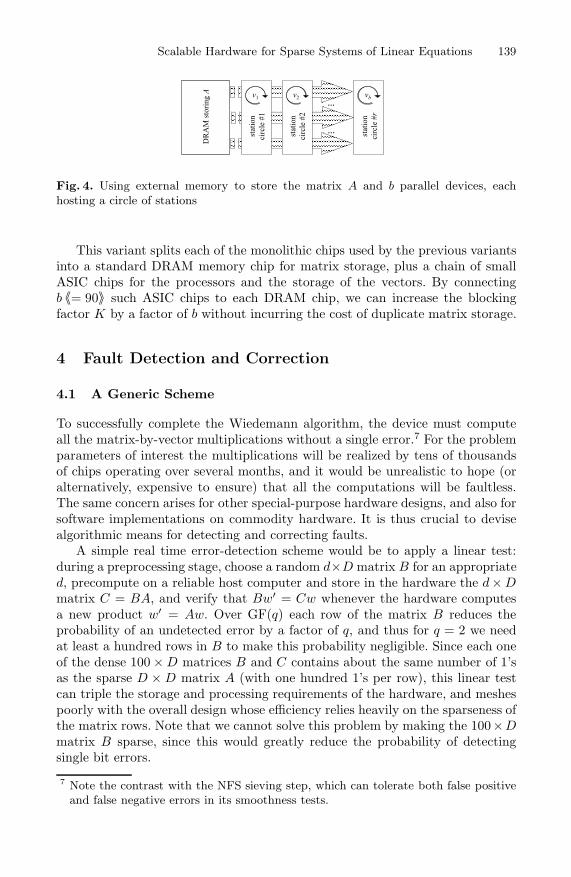
Fig. 4. Using external memory to store the matrix A and b parallel devices, eachhosting a circle of stations
This variant splits each of the monolithic chips used by the previous variantsinto a standard DRAM memory chip for matrix storage, plus a chain of smallASIC chips for the processors and the storage of the vectors. By connectingb 〈〈= 90〉〉 such ASIC chips to each DRAM chip, we can increase the blockingfactor K by a factor of b without incurring the cost of duplicate matrix storage.
4 Fault Detection and Correction
4.1 A Generic Scheme
To successfully complete the Wiedemann algorithm, the device must computeall the matrix-by-vector multiplications without a single error.7 For the problemparameters of interest the multiplications will be realized by tens of thousandsof chips operating over several months, and it would be unrealistic to hope (oralternatively, expensive to ensure) that all the computations will be faultless.The same concern arises for other special-purpose hardware designs, and also forsoftware implementations on commodity hardware. It is thus crucial to devisealgorithmic means for detecting and correcting faults.
A simple real time error-detection scheme would be to apply a linear test:during a preprocessing stage, choose a random d×D matrix B for an appropriated, precompute on a reliable host computer and store in the hardware the d × Dmatrix C = BA, and verify that Bw′ = Cw whenever the hardware computesa new product w′ = Aw. Over GF(q) each row of the matrix B reduces theprobability of an undetected error by a factor of q, and thus for q = 2 we needat least a hundred rows in B to make this probability negligible. Since each oneof the dense 100 × D matrices B and C contains about the same number of 1’sas the sparse D × D matrix A (with one hundred 1’s per row), this linear testcan triple the storage and processing requirements of the hardware, and meshespoorly with the overall design whose efficiency relies heavily on the sparseness ofthe matrix rows. Note that we cannot solve this problem by making the 100×Dmatrix B sparse, since this would greatly reduce the probability of detectingsingle bit errors.
7 Note the contrast with the NFS sieving step, which can tolerate both false positiveand false negative errors in its smoothness tests.

140 W. Geiselmann et al.
In the following we describe an alternative error-detection scheme, whichprovides (effectively) an arbitrarily small error probability at a negligible cost,under reasonable assumptions. It inspects only the computed (possibly erro-neous) matrix-by-vector products, and can thus be applied to any implementa-tion of Wiedemann’s algorithm. We will consider its operation over any finitefield GF(q), though for integer factoring via NFS only q = 2 is of interest.
Detection. Let w0, w1, w2, . . . ∈ GF(q)D denote the sequence of vectors com-puted by the device, where w0 = v. To verify that indeed wi = Aiv for all i > 0,we employ the following randomized linear test. For a small integer d 〈〈= 200〉〉,choose a single vector b ∈ GF(q)D uniformly at random, and precompute on areliable computer the single vector ct = btAd (here t denotes transpose). Aftereach wi is computed, compute also the inner products btwi and ctwi (which arejust field elements). Save the last d results of the latter in a small shift register,and after each multiplication test the following condition:
bt
wi = ct
wi−d . (2)
If equality does not hold, declare that at least one of the last d multiplicationswas faulty.
Correctness. If no faults have occurred then (2) holds since both sides equalbtAiv. Conversely, we will argue that the first faulty multiplication wj �= Awj−1will be detected within d steps with overwhelming probability, under reasonableassumptions.
Let us first demonstrate this claim in the simplest case of some transient errorε which occurs in step j. This changes the correct vector Ajv into the incorrectvector wj = Ajv + ε. All the previous wi for i < j are assumed to be correct,and all the later wi for i > j are assumed to be computed correctly, but startingwith the incorrect wj in step j. It is easy to verify that the difference betweenthe correct and incorrect values of the computed vectors wi for i > j evolves asAi−jε, and due to the randomness of the matrix A generated by the sieving stepthese error vectors are likely to point in random directions in the D-dimensionalspace GF(q)D. The device has d chances to catch the error by considering pairsof computed vectors which are d apart, with the first vector being correct andthe second vector being incorrect. The probability that all these d random errorvectors will be orthogonal to the single random test vector b is expected to beabout q−d, which is negligible; the computational cost was just two vector innerproducts per matrix-by-vector multiplication.
The analysis becomes a bit more involved when we assume that the hardwarestarts to malfunction at step j, and adds (related or independent) fault patternsto the computed result after the computation of each matrix-vector product fromstep j onwards. Let the result of the i-th multiplication be wi = Awi−1 + εi,where the vector εi is the error in the output of this multiplication. We considerthe first fault, so εi = 0 for all i < j. Assume that j ≥ d (j < d will be addressedbelow). By the linearity of the multiplication and the minimality of j, we canexpand the above recurrence to obtain wi = Aiv +
∑ii′=j(A
i−i′εi′) (i ≥ j).

Scalable Hardware for Sparse Systems of Linear Equations 141
Plugging this into (2) and canceling out the common term btAiv, we get thatfor j ≤ i < j + d, (2) is equivalent to:
bt
ri = 0 where ri =∑i
i′=j(Ai−i′
εi′) . (3)
We assume that each error εi is one of at most (qD)α possibilities for someα D/d (e.g., 〈〈α = 105〉〉), regardless of A and b. This suffices to enumerate allreasonably likely combinations of local faults (corrupted matrix entries, faultypipeline connections, errors in GF(q) multipliers, memory bit flips, etc.). We alsomake the simplifying (though not formally correct) assumption that A10, ..., Ad−1
are random matrices drawn uniformly and independently.8 Then for any fixedvalues of εi, the vectors in the set R = {ri}j+d−1
i=j+10 are drawn uniformly andindependently from GF(q)D (recall that εj �= 0), and thus the probability thatthe span of R has dimension less than |R| = d − 10 is smaller than dq−(D−d)
(which is a trivial upper bound on the probability that one of the d − 10 vectorsfalls into the span of the others). By assumption, there are at most (qD)αd
possible choices of (εi)j+di=j+1. Hence, by the union bound, the probability that
the span of R has dimension less than d − 10 is at most (qD)αd · dq−(D−d) =d · qαd logq D+d− D, which is negligible. Conditioned on the span of R having fullrank d−10, the probability of the random vector b being orthogonal to the spanof R is q−(d−10), which is also negligible. Hence, with overwhelming probability,at least one of the tests (3) for j + 10 < i < j + d will catch the fault in wj .
Startup and Finalization. Note that the test (2) applies only to i > d, andmoreover that our analysis assumes that the first d multiplications are correct.Thus, for each of the 2K multiplication chains of block Wiedemann, we startthe computation by computing the first d multiplications on a reliable general-purpose computer, and then load the state (including the queue of ctwi valuesfor i = 0, . . . , d) into the device for further multiplications.
Also note that in the analysis, the results of the j-th multiplications areimplicitly checked by (2) for i = j, . . . , j +d−1. Thus, in order to properly checkthe last d multiplications in each chain, we run the device for d extra steps anddiscard the resulting vectors but still test (2).
Recovery. The above method will detect a fault within d clock cycles (withoverwhelming probability), but will not correct it. Once the fault is detected,we must backtrack to a known-good state without undoing too much work.
8 The sieving and preprocessing steps of NFS yield a matrix A that has nearly fullrank and is“random-looking” except for some biases in the distribution of its val-ues: A is sparse (with density 〈〈≈ 100/1010〉〉) and its density is decreasing with therow number. The first few self-multiplications increase the density exponentially andsmoothen the distribution of values, so that A10 has full and uniform density. Theindependence approximation is applicable since we are looking at simple local prop-erties (corresponding to sparse error vectors), which are “mixed” well by the matrixmultiplication. While the resulting matrices do have some hidden structure, realisticfault patterns are oblivious to that structure.

142 W. Geiselmann et al.
Assuming a sufficiently low probability of error, it is simplest to dump a fullcopy of the current vector wi from the device into a general-purpose computer,at regular but generously-spaced intervals; this can be done by another specialstation tapping the pipeline. The backup vectors may be stored on magneticmedia, and thus their storage has negligible cost. When a fault is detected,the faulty component can be replaced (or a spare device substituted) and thecomputation restarted from the last known-good backup.
4.2 Device-Specific Considerations
Implementation. The above scheme requires only the computation of two in-ner products (btwi and ctwi) for each multiplication. In the proposed hardwaredevice, this is achieved by one additional station along the pipeline, which tapsthe vector entries flowing along the pipeline and verifies their correctness by theabove scheme. This station contains the entries of b and c in sequential-accessDRAM. For each of the K vectors being handled, it processes a k-tuple of vectorentries at every clock cycle, keeps the d most recent values of ctwi in a localFIFO queue at this station, and performs the test according to (2).
Halving the Cost. The storage cost can be halved by choosing b pseudoran-domly instead of purely randomly; the number of multipliers can also be nearlyhalved by choosing b to be very sparse.
Using Faulty Chips. In addition to the above high-level error-recovery scheme,it is also useful to work around local faults in the component chips: this increaseschip yield and prevents the need to disassemble multi-chip devices if a fault wasdiscovered after assembly. To this end, the proposed device offers a significantlevel of fault tolerance due to its uniform pipelined design: we can add a “bypass”switch to each station, which effectively removes it from the pipeline (apartfor some latency). Once we have mapped the faults, we can work around anyfault in the internals of some station (this includes the majority circuit area) byactivating the bypass for that station and assigning its role to one of a few sparestations added in advance. The chip containing the fault then remains usable,and only slightly less efficient.
5 Cost and Performance
5.1 Cost for 1024-Bit NFS Matrix Step
As explained in Section 2, there is considerable uncertainty about the size anddensity of the matrices that would appear in the factorization of 1024-bit com-posites using the Number Field Sieve. For concreteness and ease of comparison,throughout Section 3 and in the following we assume the rather conservative“large matrix” parameters (see Section 2).
Clearly there are many possibilities for fixing the different parameters ofour device, depending on such parameters as desired chip size and number of

Scalable Hardware for Sparse Systems of Linear Equations 143
chips. One may even consider combining the above design with the splitting ofthe processed matrix into submatrices as put forward in [10], thereby giving upthe homogeneity and purely local communication but decreasing the dimensionof the vectors that have to be handled. In the following we consider a specificparameter set, which focuses on practicality with today’s technology.
We assume 90nm chip manufacturing technology with DRAM-type process9,a net chip area of 1 cm2, a per-chip I/O bandwidth of 1024 Gbit/s, and aclock rate of 1GHz. A DRAM access is assumed to take 70 clock cycles. Theseparameters are quite realistic with current technology.
We employ a 300×90 array of ASIC chips. Each column of 300 chips containsu = 9600 stations (32 per chip). Each station consists of k = 32 processors,communicating over γ = 2 intra-station channels, with a parallelization factor of10. Each of the 300 rows, of 90 chips each, is fed by a 108Gbit DRAM module.Overall, the blocking factor is K = 10 · 90 = 900. This array can complete allmultiplication chains in ≈ 2.4 months.
The total chip area, including the matrix storage, is less than 90 full 30cmwafers. Assuming a “silicon cost” of US$ 5000 per wafer, and a factor 4 increasefor overheads such as faulty chips, packaging, testing and assembly, the totalcost is under US$ 2M.
Comparison to Previous Designs. A mesh-based design as considered in [11],adapted to 90nm technology and using 85×85 chips of size 12.25 cm2 each, willrequire about 11.7 months to process the above matrix. The higher complexityof this design limits the clocking rate to 200 MHz only. Comparing throughputper silicon area, the new device is 6.5 more efficient; it also has much smallerindividual chips and no need for non-local wiring.
Implications for 1024-Bit Factorization. With the above device and matrixsize, the cost of the NFS linear algebra step is 0.4M US$×year, which is sig-nificantly lower than that of the NFS sieving step using the TWIRL device [4].Moreover, TWIRL is expected to produce a matrix significantly smaller than theconservative estimate used above, so the cost of the linear algebra step would belower than the above estimate. Since TWIRL, being a wafer-scale design, is alsomore technologically challenging, this reaffirms the conclusion that at presentthe bottleneck of factoring large integers is the NFS sieving step [9].
5.2 Further Details
To derive concrete cost and performance estimates for the 1024-bit case, severalimplementation choices for parameters, such as δu, δf, γ, τ , have been determinedexperimentally as follows. For the above problem and technology parameters, anda large randomly drawn matrix, we used a software simulation of a station tocheck for congestions in bus and memory accesses, and chose design parametersfor which such congestions never occur experimentally. Recall that the device’s
9 Amortized DRAM density is assumed to be 0.1µm2 per bit, and the logic is assumedto have an average density of 1.4µm2 per transistor.

144 W. Geiselmann et al.
operation is deterministic and repetitive (see Section 3.4), so the simulationaccurately reflects the device’s operation with the given parameters.
In the following we briefly mention some aspects of the circuit area andits analysis, as used to derive the above estimate. Note that we employ thesplit design of Section 3.7, which puts the matrix storage in plain DRAM chipsand the logic and vector storage in ASIC chips. For these parameters, memorystorage dominates area: approximately 97% of the ASIC chip area is occupiedby the DRAM which stores the intermediate vectors (i.e., W and W ′). Thus,the suitable chip production process is a DRAM process optimized for maximummemory density (at the expense of slightly larger logic circuits); similar casesarose in previous proposals [9,10,11]. Each of the k 〈〈= 32〉〉 processors in each ofthe 32 stations in each of the 300 × 90 ASIC chips contains the following logic:
– A K/b-bit register for storing the K/b-tuples of GF(2) elements flowing alongfrom the inter-station pipeline (≈ 8 · K/b transistors).
– A K/b-bit register for each of the γ 〈〈= 2〉〉 intra-station channels (≈ 8 · γ ·K/b transistors).
– A FIFO queue of depth 〈〈2〉〉 for storing elements arriving on the inter-stationpipeline along with the number of the internal bus onto which the respectiveelement is to be written. For this ≈ 2 · 8 · (K + �log2(γ)�) transistors perqueue entry are sufficient.
– A FIFO queue of depth 〈〈4〉〉 for storing elements arriving on the intra-stationchannels that have to be XORed to the vector. Each entry consists of a K/b-tuple of bits for the vector and a row number in the submatrix handled bythe station has to be stored. This occupies ≈ 4 · 8 · (K/b + �log2�D/(ku)��)〈〈= 4 · 8 · (10 + 15)〉〉 transistors per queue entry.
In addition to the registers and queues, we need some logic for counters (to iden-tify the end of a vector and to decide when to read another element from a bus),multiplexers, etc. For the parameters of interest, < 1500 transistors are sufficientfor this. Overall, the 32 × 32 processors on each chip occupy 〈〈≈ 3.2mm2〉〉.
The DRAM needed splits into three parts.
– For storing 2·K/b vectors in GF(2)�D/(uk)�,: 2·K/b·D/(uk) bit 〈〈≈ 650 Kbit〉〉.– For the fetches table: δu + 1 + �log2(γ)� bits per entry.– For the updates table: δf + 1 + �log2(γ)� + �log2�D/(uk)�� bits per entry.
Overall, the DRAM on each chip occupies 〈〈≈ 67mm2〉〉. The time for each ofthe ≈ 2D/K matrix-by-vector multiplications is ≈ e + D/k clock cycles, wheree gives some leeway for emptying queues and internal buses (for the parameterswe are interested in e 1000 is realistic).
6 Conclusion
We have described a pipelined systolic design for the matrix-by-vector multi-plications of the block Wiedemann algorithm, which exhibits several advantagesover the prior (mesh-based) approach. It has lower cost and modest technological

Scalable Hardware for Sparse Systems of Linear Equations 145
requirements; specifically, unlike previous proposals it uses standard chip sizesand purely local communication. The architecture is scalable, and offers the flex-ibility to handle problems of varying sizes. The operation is deterministic andallows local simulation and verification of components. We have also describedan efficient error detection and recovery mechanism, which can also be adaptedto other software or hardware implementations of Wiedemann’s algorithm.
For 1024-bit RSA keys, executing the linear algebra step of the NFS usingthis device appears quite realistic with present technology, at a cost lower thanthat of the NFS sieving step.
References
1. Shamir, A.: Factoring Large Numbers with the TWINKLE Device. In: CHES1999. Volume 1717 of LNCS, Springer (1999) 2–12
2. Lenstra, A.K., Shamir, A.: Analysis and Optimization of the TWINKLE FactoringDevice. In: EUROCRYPT 2000. Volume 1807 of LNCS, Springer (2000) 35–52
3. Geiselmann, W., Steinwandt, R.: A Dedicated Sieving Hardware. In: PKC 2003.Volume 2567 of LNCS, Springer (2003) 254–266
4. Shamir, A., Tromer, E.: Factoring Large Numbers with the TWIRL Device. In:CRYPTO 2003. Volume 2729 of LNCS, Springer (2003) 1–26
5. Geiselmann, W., Steinwandt, R.: Yet Another Sieving Device. In: CT-RSA 2004.Volume 2964 of LNCS, Springer (2004) 278–291
6. Franke, J., Kleinjung, T., Paar, C., Pelzl, J., Priplata, C., Stahlke, C.: SHARK -A Realizable Special Hardware Sieving Device for Factoring 1024-bit Integers. In:SHARCS 2005. (2005)
7. Franke, J., Kleinjung, T., Paar, C., Pelzl, J., Priplata, C., Simka, M., Stahlke, C.:An Efficient Hardware Architecture for Factoring Integers with the Elliptic CurveMethod. In: SHARCS 2005. (2005)
8. Bernstein, D.J.: Circuits for Integer Factorization: a Proposal. At the time of writ-ing available electronically at http://cr.yp.to/papers/nfscircuit.pdf (2001)
9. Lenstra, A.K., Shamir, A., Tomlinson, J., Tromer, E.: Analysis of Bernstein’sFactorization Circuit. In: ASIACRYPT 2002. Volume 2501 of LNCS, Springer(2002) 1–26
10. Geiselmann, W., Steinwandt, R.: Hardware for Solving Sparse Systems of LinearEquations over GF(2). In: CHES 2003. Volume 2779 of LNCS, Springer (2003)51–61
11. Geiselmann, W., Kopfer, H., Steinwandt, R., Tromer, E.: Improved Routing-BasedLinear Algebra for the Number Field Sieve. In: Proceedings of ITCC ’05 – Trackon Embedded Cryptographic Systems, IEEE Computer Society (2005) 636–641
12. Frey, G.: A First Step Towards Computations in Brauer Groups and Applicationsto data Security. Invited talk at WARTACRYPT ’04 (2004)
13. Frey, G.: On the Relation between Brauer Groups and Discrete Logarithms. Un-published manuscript (2004)
14. Pomerance, C.: A Tale of Two Sieves. Notices of the ACM (1996) 1473–148515. Lenstra, A.K., Hendrik W. Lenstra, J., eds.: The development of the number field
sieve. Volume 1554 of Lecture Notes in Mathematics. Springer (1993)16. Coppersmith, D.: Solving Homogeneous Linear Equations over GF(2) via Block
Wiedemann Algorithm. Mathematics of Computation 62 (1994) 333–350

146 W. Geiselmann et al.
17. Villard, G.: Further analysis of Coppersmith’s block Wiedemann algorithm for thesolution of sparse linear systems. In: International Symposium on Symbolic andAlgebraic Computation — ISAAC ’97, ACM (1997) 32–39
18. Cavallar, S., Dodson, B., Lenstra, A., Lioen, W., Montgomery, P., Murphy, B.,te Riele et al., H.: Factorization of a 512-bit RSA modulus. In: EUROCRYPT2000. Volume 1807 of LNCS, Springer (2000) 1–17