lmz20502 2 a simple switcher nano module - ti.com · lmz20502 snvs852c–june 2012–revised april...
TRANSCRIPT

40
45
50
55
60
65
70
75
80
85
90
95
100
0.01 0.1 1 10
Effi
cien
cy (
%)
Output Current (A)
3V4.2V5V
C001
VIN
CIN
COUT
RFBT
RFBB
LMZ20502VIN
EN VOUT
FBGND MODE PG
CFF
VOUT
Product
Folder
Sample &Buy
Technical
Documents
Tools &
Software
Support &Community
LMZ20502SNVS852C –JUNE 2012–REVISED APRIL 2015
LMZ20502 2 A SIMPLE SWITCHER® Nano Module1 Features 3 Description
The LMZ20502 SIMPLE SWITCHER® Nano Module1• Integrated Inductor
regulator is an easy-to-use synchronous step-down• Miniature 3.5 mm x 3.5 mm x 1.75 mm Package DC-DC converter capable of driving up to 2 A of load• 2 A Maximum Load Current from an input of up to 5.5 V, with exceptional
efficiency and output accuracy in a very small• Input Voltage Range of 2.7 V to 5.5 Vsolution size. The innovative package contains the• Adjustable Output Voltage Range of 0.8 V to 3.6 V regulator and inductor in a small 3.5 mm x 3.5 mm x
• ± 1% Feedback Tolerance Over Temperature 1.75 mm volume, thus saving board space andeliminating the time and expense of inductor• 2.4 µA (max) Quiescent Current In Shutdownselection. The LMZ20502 requires only five external• 3 MHz Fixed PWM Switching Frequencycomponents and has a pin-out designed for simple,• -40°C to 125°C Junction Temperature Range optimum PCB layout. The LMZ20502 is a member of
• Power Good Flag Function Texas Instruments' SIMPLE SWITCHER family. TheSIMPLE SWITCHER concept provides for an easy to• Pin-Selectable Switching Modesuse complete design with a minimum number of• Internal Compensation and Soft-Start external components and the TI WEBENCH® design
• Current Limit, Thermal Shutdown, and UVLO tool. TI's WEBENCH tool includes features such asProtection external component calculation, electrical simulation,
and WebTherm™. For soldering information, pleaserefer to the following document: SNOA401.2 Applications
• Point of Load Regulation Device Information(1)
• Space Constrained Applications PACKAGE /PART NUMBER BODY SIZE (NOM)DRAWINGLMZ20502SILT USIP (8) / SIL0008F 3.50 mm x 3.50 mm
(1) For all available packages, see the orderable addendum atthe end of the datasheet.
Typical Efficiency for VOUT = 1.8 V Auto Mode4 Simplified Schematic
1
An IMPORTANT NOTICE at the end of this data sheet addresses availability, warranty, changes, use in safety-critical applications,intellectual property matters and other important disclaimers. PRODUCTION DATA.

LMZ20502SNVS852C –JUNE 2012–REVISED APRIL 2015 www.ti.com
Table of Contents8.4 Device Functional Modes........................................ 131 Features .................................................................. 1
9 Application and Implementation ........................ 152 Applications ........................................................... 19.1 Application Information............................................ 153 Description ............................................................. 19.2 Typical Application ................................................. 164 Simplified Schematic............................................. 19.3 Do's and Don'ts ...................................................... 235 Revision History..................................................... 2
10 Power Supply Recommendations ..................... 236 Pin Configuration and Functions ......................... 311 Layout................................................................... 247 Specifications......................................................... 4
11.1 Layout Guidelines ................................................. 247.1 Absolute Maximum Ratings ...................................... 411.2 Layout Example .................................................... 257.2 ESD Ratings ............................................................ 411.3 Soldering Information ............................................ 257.3 Recommended Operating Conditions....................... 4
12 Device and Documentation Support ................. 277.4 Thermal Information .................................................. 512.1 Device Support...................................................... 277.5 Electrical Characteristics........................................... 612.2 Trademarks ........................................................... 277.6 System Characteristics ............................................ 712.3 Electrostatic Discharge Caution............................ 277.7 Typical Characteristics .............................................. 812.4 Glossary ................................................................ 278 Detailed Description .............................................. 9
13 Mechanical, Packaging, and Orderable8.1 Overview ................................................................... 9Information ........................................................... 288.2 Functional Block Diagram ......................................... 913.1 Package Option Addendum .................................. 298.3 Feature Description................................................... 9
5 Revision History
Changes from Revision B (December 2014) to Revision C Page
• Added the package option addendum manually ................................................................................................................... 1
Changes from Revision A (July 2013) to Revision B Page
• Changed Device Information and Handling Rating tables, Feature Description, Device Functional Modes,Application and Implementation, Power Supply Recommendations, Layout, Device and Documentation Support, andMechanical, Packaging, and Orderable Information sections; moved some curves to Application Curves section .............. 1
2 Submit Documentation Feedback Copyright © 2012–2015, Texas Instruments Incorporated
Product Folder Links: LMZ20502

1
2
3
4 5
6
7
8PG
ENMODE
FB VOUT
GND
VINNC
LMZ20502www.ti.com SNVS852C –JUNE 2012–REVISED APRIL 2015
6 Pin Configuration and Functions
USIP Package (SIL)8 Pins
Top View
Pin FunctionsPIN
TYPE (1) DESCRIPTIONNUMBER NAME
1 PG O Power good flag; open drain. Connect to logic supply through a resistor. High = power good; Low =power bad. If not used, leave unconnected.
2 EN I Enable input. High = On, Low = Off. A valid input voltage, on pin 8, must be present before EN isasserted. Do not float.
3 MODE I Mode selection input. High = forced PWM. Low = AUTO mode, with PFM at light load . Do not float.4 FB I Feedback input to controller. Connect to output through feedback divider.5 VOUT P Regulated output voltage; connect to COUT.6 GND G Ground for all circuitry. Reference point for all voltages.7 NC This pin must be left floating. Do not connect to ground or any other node.8 VIN P Input supply to regulator. Connect to input capacitor(s) as close as possible to the VIN pin and GND
pin of the module.EP EP G Ground and heat-sink connection. See Layout Guidelines section for more information.
(1) G = Ground, I = Input, O = Output, P = Power
Copyright © 2012–2015, Texas Instruments Incorporated Submit Documentation Feedback 3
Product Folder Links: LMZ20502

LMZ20502SNVS852C –JUNE 2012–REVISED APRIL 2015 www.ti.com
7 Specifications
7.1 Absolute Maximum RatingsUnder the recommended operating junction temperature range of -40°C to 125°C (unless otherwise noted) (1)
MIN MAX UNITVIN to GND –0.2 6EN, MODE, FB, PG, to GND (2) –0.2 VIN+0.2 VVOUT to GND (2) –0.2 VIN+0.2Junction temperature 150 °CPeak soldering reflow temperature for Pb (3) 240
°CPeak soldering reflow temperature for No-Pb (3) 260Storage temperature range –65 150 °C
(1) Stresses beyond those listed under Absolute Maximum Ratings may cause permanent damage to the device. These are stress ratingsonly, which do not imply functional operation of the device at these or any other conditions beyond those indicated under RecommendedOperating Conditions. Exposure to absolute-maximum-rated conditions for extended periods may affect device reliability.
(2) The absolute maximum voltage on this pin must not exceed 6V with respect to ground. Do not allow the voltage on the output pin toexceed the voltage on the input pin by more than 0.2 V.
(3) For soldering information, please refer to the following document: SNOA401.
7.2 ESD RatingsVALUE UNIT
Human body model (HBM), per ANSI/ESDA/JEDEC JS-001, all pins (1) ±2000V(ESD) Electrostatic discharge VCharged-device model (CDM), per JEDEC specification JESD22-C101, ±500
all pins (2)
(1) JEDEC document JEP155 states that 500-V HBM allows safe manufacturing with a standard ESD control process.(2) JEDEC document JEP157 states that 250-V CDM allows safe manufacturing with a standard ESD control process.
7.3 Recommended Operating ConditionsUnder the recommended operating junction temperature range of -40°C to 125°C (unless otherwise noted) (1)
MIN NOM MAX UNITInput voltage 2.7 5.5 VOutput voltage programming 0.8 3.6 VOutput voltage range (2) 0 3.6 VLoad current 0 2 APower good flag current 0 4 mAJunction temperature -40 125 °C
(1) Stresses beyond those listed under Absolute Maximum Ratings may cause permanent damage to the device. These are stress ratingsonly, which do not imply functional operation of the device at these or any other conditions beyond those indicated under RecommendedOperating Conditions. Exposure to absolute-maximum-rated conditions for extended periods may affect device reliability.
(2) Under no conditions should the output voltage be allowed to fall below zero volts.
4 Submit Documentation Feedback Copyright © 2012–2015, Texas Instruments Incorporated
Product Folder Links: LMZ20502

LMZ20502www.ti.com SNVS852C –JUNE 2012–REVISED APRIL 2015
7.4 Thermal InformationLMZ20502
THERMAL METRIC (1) USIP (SIL) UNIT8 PINS
RθJA Junction-to-ambient thermal resistance 42.6RθJC(top) Junction-to-case (top) thermal resistance 20.8RθJB Junction-to-board thermal resistance 9.4
°C/WψJT Junction-to-top characterization parameter 1.5ψJB Junction-to-board characterization parameter 9.3RθJC(bot) Junction-to-case (bottom) thermal resistance 1.8
(1) The values given in this table are only valid for comparison with other packages and can not be used for design purposes. For designinformation please see the Maximum Ambient Temperature section. For more information about traditional and new thermal metrics, seethe IC Package Thermal Metrics application report, SPRA953.
Copyright © 2012–2015, Texas Instruments Incorporated Submit Documentation Feedback 5
Product Folder Links: LMZ20502

LMZ20502SNVS852C –JUNE 2012–REVISED APRIL 2015 www.ti.com
7.5 Electrical CharacteristicsLimits apply over the recommended operating junction temperature range of –40°C to 125°C, unless otherwise noted.Minimum and maximum limits are verified through test, design, or statistical correlation. Typical values represent the mostlikely parametric norm at TJ = 25°C, and are provided for reference purposes only. Unless otherwise stated the followingconditions apply: VIN = 3.6 V
PARAMETER TEST CONDITIONS MIN (1) TYP MAX (1) UNITVFB Feedback voltage VIN = 3.6 V 0.594 0.6 0.606 VIQ_AUTO Operating quiescent current in AUTO mode, VFB = 0.8V 72 90 µAAUTO modeIQ_PWM Operating quiescent current in PWM mode, VFB = 0.8V 490 620 µAforced PWM modeIQ_off Shutdown quiescent current (2) VIN = 3.6 V, VEN = 0.0 V 0.7 1.5
µAVIN = 5.5 V, VEN = 0.0 V 1.0 2.4
VUVLO Input supply under-voltage Rising 2.5Vlock-out thresholds Falling 2.3
VEN High Level Input Voltage VIH 1.4V
Low Level Input Voltage VIL 0.4VMODE High Level Input Voltage VIH 1.2
VLow Level Input Voltage VIL 0.4
I LIM Peak switch current limit (3) 2.1 2.7 AFosc Internal oscillator frequency 2.5 3.0 3.2 MHzTON Minimum switch on-time (4) 50 nsTss Soft start time (4) 800 µsRPG Power good flag pull-down 40 70 110 ΩRdson
VPG1 Power good flag, under- % of feedback voltage, rising 92%voltage trip (5)
VPG2 Power good flag, under- % of feedback voltage, falling 88%voltage trip (5)
VPG3 Power good flag, over-voltage % of feedback voltage, rising 112%trip (5)
VPG4 Power good flag, over-voltage % of feedback voltage, falling 108%trip (5)
TSD Thermal shutdown (4) Rising threshold 159 °CThermal shutdown 15 °Chysteresis (4)
(1) MIN and MAX limits are 100% production tested at 25°C. Limits over the operating temperature range are verified through correlationusing Statistical Quality Control (SQC) methods. Limits are used to calculate Average Outgoing Quality Level (AOQL).
(2) Shutdown current includes leakage current of the switching transistors.(3) This is the peak switch current limit measured with a slow current ramp. Due to inherent delays in the current limit comparator, the peak
current limit measured at 3MHz will be larger.(4) This parameter is not tested in production.(5) See Power Good Flag Function for explanation of voltage levels.
6 Submit Documentation Feedback Copyright © 2012–2015, Texas Instruments Incorporated
Product Folder Links: LMZ20502

LMZ20502www.ti.com SNVS852C –JUNE 2012–REVISED APRIL 2015
7.6 System CharacteristicsThe following specifications apply to the circuit found in Figure 16 with the appropriate modifications from Table 2. Theseparameters are not tested in production and represent typical performance only. Unless otherwise stated the followingconditions apply: TA = 25°C.
PARAMETER TEST CONDITIONS MIN TYP MAX UNITVOUT = 1.2 V, 0.4%VIN = 5 V, IOUT = 0 A to 2 A, PWM
Load Percent output voltage change VOUT = 1.8 V 0.4%Regulation for the given load current change VIN = 5 V, IOUT = 0 A to 2 A, PWMVOUT = 3.3 V 0.2%VIN = 5 V, IOUT = 0 A to 2 A, PWMVOUT = 1.2 V 0.2%IOUT = 2 A, VIN = 3 V to 5 V, PWM
Percent output voltage changeLine VOUT = 1.8 Vfor the given change in input 0.15%Regulation IOUT = 2 A, VIN = 3 V to 5 V, PWMvoltageVOUT = 3.3 V 0.18%IOUT = 2 A,VIN = 4 V to 5 V, PWMVOUT = 1.2 V 3.3IOUT = 1 A, VIN = 5 V, PWMVOUT = 1.8 VVR-PWM Output voltage ripple in PWM 3.3 mV pk-pkIOUT = 1 A, VIN = 5 V, PWMVOUT = 3.3V 4.2IOUT= 1 A, VIN = 5 V, PWMVOUT = 1.2V 22IOUT= 1 mA, VIN = 3 V, PFMVOUT = 1.8 VVR-PFM Output voltage ripple in PFM 22 mV pk-pkIOUT= 1 mA, VIN=3 V, PFMVOUT = 3.3 V 40IOUT = 1 mA, VIN = 5 V, PFMVOUT = 1.2 VVIN = 5 V, IOUT = 0 A to 2 A, Tr = Tf = 2 µs, ±115PWM
Output voltage deviation from VOUT = 1.8 VLoad nominal due to a load current VIN = 5 V, IOUT = 0 A to 2 A, Tr = Tf = 2 µs, ±100 mVTransient step PWMVOUT = 3.3 VVIN = 5 V, IOUT = 0 A to 2 A, Tr = Tf = 2 µs, ±150PWMVOUT = 1.2VIOUT = 1 A, VIN = 3 V to 5 V, Tr = Tf = 50 25µs, PWMVOUT = 1.8 VLine Output voltage deviation due to IOUT = 1 A, VIN = 3 V to 5 V, Tr = Tf = 50 30 mV pk-pkTransient an input voltage step µs, PWMVOUT = 3.3 VIOUT = 1 A, VIN = 4 V to 5 V, Tr = Tf = 50 20µs, PWMVOUT = 1.2 V 87%VIN = 3 VVOUT = 1.8 VPeak efficiency 91%VIN = 3 VVOUT = 3.3 V 94%VIN = 4.2 V
ηVOUT = 1.2 V 74%VIN = 3 V, IOUT = 2 AVOUT = 1.8 VFull load efficiency 79%VIN = 3 V, IOUT = 2 AVOUT = 3.3 V 89%VIN = 4.2 V, IOUT = 2 A
Copyright © 2012–2015, Texas Instruments Incorporated Submit Documentation Feedback 7
Product Folder Links: LMZ20502

Input Voltage (V)
Inpu
t Cur
rent
(µ
A)
2 2.5 3 3.5 4 4.5 5 5.5 640
45
50
55
60
65
70
75
80
D005
-40°C27°C90°C
Input Voltage (V)
Inpu
t Cur
rent
(m
A)
2 2.5 3 3.5 4 4.5 5 5.5 60.3
0.35
0.4
0.45
0.5
0.55
0.6
D006
-40°C27°C90°C
Temperature (°C)
EN
Inpu
t Thr
esho
lds
(V)
-40 -20 0 20 40 60 80 1000.4
0.5
0.6
0.7
0.8
0.9
1
D003
RisingFalling
Temperature (°C)
MO
DE
Inpu
t Thr
esho
lds
(V)
-40 -20 0 20 40 60 80 1000.4
0.5
0.6
0.7
0.8
0.9
1
D004
RisingFalling
Temperature (°C)
Out
put V
olta
ge (
V)
-40 -20 0 20 40 60 80 1001.76
1.77
1.78
1.79
1.8
1.81
1.82
D001
Iout = 0 AIout = 1 A
Input Voltage (V)
Sw
itchi
ng F
requ
ency
(M
Hz)
2 2.5 3 3.5 4 4.5 5 5.5 62.6
2.65
2.7
2.75
2.8
2.85
2.9
2.95
3
3.05
3.1
3.15
3.2
D002
-40°C27°C90°C
LMZ20502SNVS852C –JUNE 2012–REVISED APRIL 2015 www.ti.com
7.7 Typical CharacteristicsUnless otherwise specified the following conditions apply: VIN = 3.6 V, TA = 25°C.
VIN = 3.6 V PWM Mode VOUT = 1.8 V VIN = 3.6 V IOUT = 0 A PWM Mode
Figure 1. Typical Output Voltage vs Temperature Figure 2. Switching Frequency in PWM Mode
VIN = 3.6 V VIN = 3.6 V
Figure 3. EN Input Thresholds Figure 4. MODE Input Thresholds
VFB = 0.8 V AUTO Mode VFB = 0.8 V PWM Mode
Figure 5. Non-Switching Input Current in AUTO Mode Figure 6. Non-Switching Input Current in PWM Mode
8 Submit Documentation Feedback Copyright © 2012–2015, Texas Instruments Incorporated
Product Folder Links: LMZ20502

LMZ20502www.ti.com SNVS852C –JUNE 2012–REVISED APRIL 2015
8 Detailed Description
8.1 OverviewThe LMZ20502 SIMPLE SWITCHER Nano Module is a voltage mode buck regulator with an integrated inductor.Input voltage feed-forward is used to compensate for loop gain variation with input voltage. Two operating modesallow the user to tailor the regulator to their specific requirements. In forced PWM mode, the regulator operatesas a full synchronous device with a 3 MHz (typ.) switching frequency and very low output voltage ripple. In AUTOmode, the regulator moves into PFM when the load current drops below the mode change threshold (seeApplication Curves). In PFM, the device regulates the output voltage between wider ripple limits than in PWM.This results in much smaller supply current than in PWM, at light loads and high efficiency. A simplified blockdiagram is shown in Functional Block Diagram.
8.2 Functional Block Diagram
8.3 Feature Description
8.3.1 Nano Scale PackageThe LMZ20502 incorporates world class package technology to provide a 2 A power supply with a total volumeof only 21 mm3 (excluding external components). All that is required for a complete power supply is the additionof feed-back resistors to set the output voltage and the input and output filter capacitors. Figure 7 and Figure 8show the LMZ20502 package. The regulator die is embedded into a PCB substrate while the power inductor ismounted on top. Vias and copper clad are used to make the connections to the die, inductor and the externalcomponents. This package is MSL3 compliant.
Copyright © 2012–2015, Texas Instruments Incorporated Submit Documentation Feedback 9
Product Folder Links: LMZ20502

INDUCTOREMBEDDEDREGULATOR
DIESUBSTRATE
PCB
Copper Clad
Via
LMZ20502SNVS852C –JUNE 2012–REVISED APRIL 2015 www.ti.com
Feature Description (continued)
Figure 7. Package Photo
Figure 8. Package Side View Drawing
8.3.2 Internal Synchronous RectifierThe LMZ20502 uses an internal NMOS FET as a synchronous rectifier to minimize switch voltage drop andincrease efficiency. The NMOS is designed to conduct through its body diode during switch dead time. This deadtime is imposed to prevent supply current "shoot-through".
8.3.3 Current Limit ProtectionThe LMZ20502 incorporates cycle-by-cycle peak current limit on both the high and low side MOSFETs. Thisfeature limits the output current in case the output is overloaded. During the overload, the peak inductor currentis limited to that value found in the Electrical Characteristics table under the heading of "ILIM".
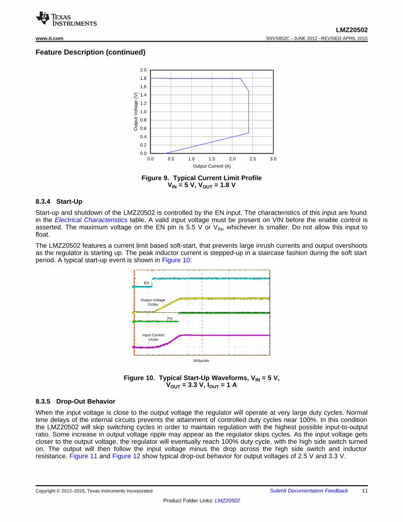
In addition to current limit, a short circuit protection mode is also implemented. When the feedback voltage isbrought down to less than 300 mV, but greater than 150 mV, by a short circuit, the synchronous rectifier is turnedoff. This provides more voltage across the inductor to help maintain the required volt-second balance. If a"harder" short brings the feedback voltage to below 150 mV, the current limit and switching frequency are bothreduced to about ½ of the nominal values. In addition, when the current limit is tripped, the device stopsswitching for about 85 µs. At the end of the time-out, switching resumes and the cycle repeats until the short isremoved.
The effect of both overload and short circuit protection can be seen in Figure 9. This graph demonstrates that thedevice will supply slightly more than 2 A to the load when in overload and much less current during fold-backmode. This is typical behavior for any regulator with this type of current limit protection.
10 Submit Documentation Feedback Copyright © 2012–2015, Texas Instruments Incorporated
Product Folder Links: LMZ20502
500µs/div
Output Voltage2V/div
PG
EN
Input Current1A/div
0.0
0.2
0.4
0.6
0.8
1.0
1.2
1.4
1.6
1.8
2.0
0.0 0.5 1.0 1.5 2.0 2.5 3.0
Out
put
Vol
tage
(V
)
Output Current (A) C001
LMZ20502www.ti.com SNVS852C –JUNE 2012–REVISED APRIL 2015
Feature Description (continued)
Figure 9. Typical Current Limit ProfileVIN = 5 V, VOUT = 1.8 V
8.3.4 Start-UpStart-up and shutdown of the LMZ20502 is controlled by the EN input. The characteristics of this input are foundin the Electrical Characteristics table. A valid input voltage must be present on VIN before the enable control isasserted. The maximum voltage on the EN pin is 5.5 V or VIN, whichever is smaller. Do not allow this input tofloat.
The LMZ20502 features a current limit based soft-start, that prevents large inrush currents and output overshootsas the regulator is starting up. The peak inductor current is stepped-up in a staircase fashion during the soft startperiod. A typical start-up event is shown in Figure 10:
Figure 10. Typical Start-Up Waveforms, VIN = 5 V,VOUT = 3.3 V, IOUT = 1 A
8.3.5 Drop-Out BehaviorWhen the input voltage is close to the output voltage the regulator will operate at very large duty cycles. Normaltime delays of the internal circuits prevents the attainment of controlled duty cycles near 100%. In this conditionthe LMZ20502 will skip switching cycles in order to maintain regulation with the highest possible input-to-outputratio. Some increase in output voltage ripple may appear as the regulator skips cycles. As the input voltage getscloser to the output voltage, the regulator will eventually reach 100% duty cycle, with the high side switch turnedon. The output will then follow the input voltage minus the drop across the high side switch and inductorresistance. Figure 11 and Figure 12 show typical drop-out behavior for output voltages of 2.5 V and 3.3 V.
Copyright © 2012–2015, Texas Instruments Incorporated Submit Documentation Feedback 11
Product Folder Links: LMZ20502

2.0
2.2
2.4
2.6
2.8
3.0
3.2
3.4
3.6
2.6 2.8 3.0 3.2 3.4 3.6 3.8 4.0
Out
put
Vol
tage
(V
)
Input Voltage (V)
0A0.5A1A2A
C001
1.9
2.0
2.1
2.2
2.3
2.4
2.5
2.6
2.0 2.2 2.4 2.6 2.8 3.0 3.2 3.4 3.6 3.8 4.0
Out
put
Vol
tage
(V
)
Input Voltage (V)
0A0.5A1A2A
C001
LMZ20502SNVS852C –JUNE 2012–REVISED APRIL 2015 www.ti.com
Feature Description (continued)Since the internal gate drive levels of the LMZ20502 are dependent on input voltage, the Rdson of the powerFETs will increase at low input voltages. This will result in degraded efficiency at output currents of greater than 1A and input voltages below about 2.9 V. Also, combinations of low input voltage and high output voltageincreases the effective switch duty cycle which may result in increased output voltage ripple.
Figure 11. Typical Drop-Out Behavior, VOUT = 2.5 V
Figure 12. Typical Drop-Out Behavior, VOUT = 3.3 V
8.3.6 Power Good Flag FunctionThe operation of the power good flag function is described in the diagram shown in Figure 13.
12 Submit Documentation Feedback Copyright © 2012–2015, Texas Instruments Incorporated
Product Folder Links: LMZ20502

VOUT
PGOOD
High = Good
Low = Bad
PG1 = 92%
PG2 = 88%
PG3 = 112%
PG4 = 108%
LMZ20502www.ti.com SNVS852C –JUNE 2012–REVISED APRIL 2015
Feature Description (continued)
Figure 13. Typical Power Good Flag Operation
This output consists of an open drain NMOS with an Rdson of about 70 Ω. When used, the power good flagshould be connected to a logic supply through a pull-up resistor. It can also be pulled-up to either VIN or VOUT,through an appropriate resistor, as desired. If this function is not needed, the PG output should be left floating.The current through this flag pin should be limited to less than 4 mA. A pull-up resistor of ≥1.5 kΩ will satisfy thisrequirement. When the EN input is pulled low, the PG flag output will also be forced low, assuming a valid inputvoltage is present at the VIN pin.
8.3.7 Thermal ShutdownThe LMZ20502 incorporates a thermal shutdown feature to protect the device from excessive die temperatures.The device will stop switching when the internal die temperature reaches about 159°C. Switching will resumewhen the die temperature drops to about 144°C.
8.4 Device Functional ModesPlease refer to Table 1 and the following paragraphs for a detailed description of the functional modes of theLMZ20502. These modes are controlled by the MODE input as shown in Table 1. The maximum voltage on theMODE pin is 5.5 V or VIN, whichever is smaller. This input must not be allowed to float.
Table 1. Mode SelectionMODE PIN VOLTAGE OPERATION
Forced PWM: The regulator operates in constant frequency, PWM mode for all loads from> 1.2 V no-load to full load; no diode emulation is used.AUTO Mode: The regulator operates in constant frequency mode for loads greater than the
< 0.4 V mode change threshold. For loads less than the mode change threshold, the regulatoroperates in PFM with diode emulation.
Copyright © 2012–2015, Texas Instruments Incorporated Submit Documentation Feedback 13
Product Folder Links: LMZ20502

Input Voltage (V)
Inpu
t Sup
ply
Cur
rent
(µ
A)
2.5 3 3.5 4 4.5 5 5.570
72
74
76
78
80
82
84
86
88
90
D007
VOUT = 1.8 VVOUT = 3.3 V
Output Voltage50mV/div
Switch Voltage2V/div
20µs/div
LMZ20502SNVS852C –JUNE 2012–REVISED APRIL 2015 www.ti.com
8.4.1 PWM OperationIn forced PWM mode, the converter operates as a constant frequency voltage mode regulator with input voltagefeed-forward. This provides excellent line and load regulation and low output voltage ripple. This operation ismaintained, even at no-load, by allowing the inductor current to reverse its normal direction. While in PWM mode,the output voltage is regulated by switching at a constant frequency and modulating the duty cycle to control thepower to the load. This mode trades off reduced light load efficiency for low output voltage ripple and constantswitching frequency. In this mode, a negative current limit of about 750mA is imposed to prevent damage to theregulator power FETs.
8.4.2 PFM OperationWhen in AUTO mode, and at light loads, the device enters PFM. The regulator estimates the load current bymeasuring both the high side and low side switch currents. This estimate is only approximate, and the exact loadcurrent threshold, to trigger PFM, can vary greatly with input and output voltage. The Application Curves showmode change thresholds for several typical operating points. When the regulator detects this threshold, thereference voltage is increased by approximately 10 mV. This causes the output voltage to rise to meet the newregulation point. When this point is reached, the converter stops switching and much of the internal circuitry isshut off, while the reference is returned to the PWM value. This saves supply current while the output voltagenaturally starts to fall under the influence of the load current. When the output voltage reaches the PWMregulation point, switching is again started and the reference voltage is again increased by about 10 mV; thusstarting the next cycle. Typical waveforms are shown in Figure 14:
Figure 14. Typical PFM Mode Waveforms: VIN = 3.6 V,VOUT = 1.8 V, IOUT = 10 mA
Figure 15. Typical No Load Input Supply Current
14 Submit Documentation Feedback Copyright © 2012–2015, Texas Instruments Incorporated
Product Folder Links: LMZ20502

LMZ20502www.ti.com SNVS852C –JUNE 2012–REVISED APRIL 2015
The actual output voltage ripple will depend on the feedback divider ratio and on the delay in the PFMcomparator. The frequency of the PFM "bursts" will depend on the input voltage, output voltage, load and outputcapacitor. Within each "burst" the device switches at 3 MHz (typ.). If the load current increases above thethreshold, normal PWM operation is resumed. This mode provides high light load efficiency by reducing theamount of supply current required to regulate the output at small load currents. This mode trades off very goodlight load efficiency for larger output voltage ripple and variable switching frequency. An example of the typicalinput supply current, while regulating with no load, is shown in Figure 15.
Because of normal part-to-part variation, the LMZ20502 may not switch into PFM mode at high input voltages.This may be seen with output voltages of about 1.2 V and below, at input voltages of about 4.2 V and above.
9 Application and Implementation
NOTEInformation in the following applications sections is not part of the TI componentspecification, and TI does not warrant its accuracy or completeness. TI’s customers areresponsible for determining suitability of components for their purposes. Customers shouldvalidate and test their design implementation to confirm system functionality.
9.1 Application InformationThe LMZ20502 is a step down DC-to-DC regulator. It is typically used to convert a higher DC voltage to a lowerDC voltage with a maximum output current of 2 A. The following design procedure can be used to selectcomponents for the LMZ20502. Alternately, the WEBENCH design tool may be used to generate a completedesign. WEBENCH utilizes an iterative design procedure and has access to a comprehensive database ofcomponents. This allows the tool to create an optimized design and allows the user to experiment with variousdesign options.
Copyright © 2012–2015, Texas Instruments Incorporated Submit Documentation Feedback 15
Product Folder Links: LMZ20502

VIN
CIN
COUT
RFBT
RFBB
LMZ20502
VIN
EN
VOUT
FBGND
MODE
PG
CFF
40.2k
80.6k
10µF
16pF
2x10µF
VOUT
1.8V @ 2A
2.7V to 5.5V
µC
I/O
I/O
RESET
100k
VIN
CIN
COUT
RFBT
RFBB
LMZ20502VIN
EN VOUT
FBGND MODE PG
CFF
40.2k
80.6k
10µF
16pF
2x10µF
VOUT
1.8V @ 2A2.7V to 5.5V
LMZ20502SNVS852C –JUNE 2012–REVISED APRIL 2015 www.ti.com
9.2 Typical ApplicationFigure 16 shows the minimum required application circuit, set up for a 1.8 V output. Figure 17 shows a fullfeatured application circuit. Please refer to Figure 16 and Figure 17 during the following design procedures.
Figure 16. LMZ20502 Typical ApplicationVOUT = 1.8 V
Figure 17. LMZ20502 Full Featured Application
16 Submit Documentation Feedback Copyright © 2012–2015, Texas Instruments Incorporated
Product Folder Links: LMZ20502

FBTOUT
FBB R0.6V
0.6R
LMZ20502www.ti.com SNVS852C –JUNE 2012–REVISED APRIL 2015
Typical Application (continued)9.2.1 Detailed Design ProcedurePlease refer to Table 2 while following the detailed design procedure. This procedure applies to both Figure 16and to Figure 17. Also, the Application Curves apply to both schematics.
Table 2. Recommended Component Values (1)
VOUT (V) RFBB (kΩ) RFBT (kΩ) COUT (µF) EFFECTIVE COUT(µF) (2) CFF (pF) CIN (µF) EFFECTIVE CIN (µF) (2)
0.8 121 40.2 2 x 10 18 µF 39 2 x 10 141.2 30.1 30.1 10 8.8 µF 20 2 x 10 141.8 40.2 80.6 10 8.4 µF 16 2 x 10 142.5 47.5 150 10 7.8 µF 12 2 x 10 143.3 53.2 237 10 7.1 µF 82 2 x 10 143.6 53.2 267 10 6.8 µF 82 2 x 10 14
(1) CIN = COUT = 10 µF, 16 V, 0805, X7R, Samsung CL21B106KOQNNNE. COUT measured at VOUT; CIN measured at 3.3 V.(2) The effective value takes into account the capacitor voltage coefficient.
9.2.1.1 Setting The Output VoltageThe LMZ20502 regulates its feedback voltage to 0.6 V (typ). A feedback divider, shown in Figure 16, is used toset the desired output voltage. Equation 1 can be used to select RFBB .
(1)
For best results, RFBT should be chosen between 30 kΩ and 300 kΩ. See Table 2 for recommended values fortypical output voltages.
9.2.1.2 Output and Feed-Forward CapacitorsThe LMZ20502 is designed to work with low ESR ceramic capacitors. The effective value of these capacitors isdefined as the actual capacitance under voltage bias and temperature. All ceramic capacitors have large voltagecoefficients, in addition to normal tolerances and temperature coefficients. Under D.C. bias, the capacitancevalue drops considerably. Larger case sizes and/or higher voltage capacitors are better in this regard. To helpmitigate these effects, multiple small capacitors can be used in parallel to bring the minimum effectivecapacitance up to the desired value. This can also ease the RMS current requirements on a single capacitor.Typically, 10 V, X5R, 0805 capacitors are adequate for the output, while 16-V caps may be used on the input.Some recommended component values are provided in Table 2. Also, shown are the measured values ofeffective input and output capacitance for the given capacitor. If smaller values of output capacitance are used,CFF must be adjusted to give good phase margin. In any case, load transient response will be compromised withlower values of output capacitance. Values much lower than those found in Table 2 should be avoided.
In practice, the output capacitor and CFF, are adjusted for the best transient response and highest loop phasemargin. Load transient testing and Bode plots are the best way to validate any given design. Application reportSLVA289 should prove helpful when optimizing the feed-forward capacitor. Also, SNVA364 details a simplemethod of creating a Bode plot with basic laboratory equipment. The values of CFF found in Table 2 provide agood starting point.
A careful study of the temperature and bias voltage variation of any candidate ceramic capacitor should be madein order to ensure that the minimum values of effective capacitance are provided. The best way to obtain anoptimum design is to use the Texas Instruments WEBENCH tool.
The maximum value of total output capacitance should be limited to between 100 µF and 200 µF. Large valuesof output capacitance can prevent the regulator from starting-up correctly and adversely affect the loop stability. Ifvalues in the range given above, or larger, are to be used, then a careful study of start-up at full load and loopstability must be performed.
Copyright © 2012–2015, Texas Instruments Incorporated Submit Documentation Feedback 17
Product Folder Links: LMZ20502

OUT-$
AJOUT V
1
1
R
TTI
2
II OUT
RMS |
LMZ20502SNVS852C –JUNE 2012–REVISED APRIL 2015 www.ti.com
9.2.1.3 Input CapacitorsThe ceramic input capacitors provide a low impedance source to the regulator in addition to supplying ripplecurrent and isolating switching noise from other circuits. An effective value of at least 14 µF is normally sufficientfor the input capacitor. If the main input capacitor(s) can not be placed close to the module, then a small 10 nF to100 nF capacitor should be placed directly at the module, across the supply and ground pins.
Many times it is desirable to use an electrolytic capacitor on the input, in parallel with the ceramics. This isespecially true if long leads/traces are used to connect the input supply to the regulator. The moderate ESR ofthis capacitor can help damp any ringing on the input supply caused by long power leads. This method can alsohelp to reduce voltage spikes that may exceed the maximum input voltage rating of the LMZ20502. The use ofthis additional capacitor will also help with voltage dips caused by input supplies with unusually high impedance.
Most of the switching current passes through the input ceramic capacitor(s). The approximate RMS value of thiscurrent can be calculated with Equation 2 and should be checked against the manufactures maximum ratings.
(2)
9.2.1.4 Maximum Ambient TemperatureAs with any power conversion device, the LMZ20502 will dissipate internal power while operating. The effect ofthis power dissipation is to raise the internal temperature of the converter, above ambient. The internal dietemperature is a function of the ambient temperature, the power loss and the effective thermal resistance RθJA ofthe device and PCB combination. The maximum internal die temperature for the LMZ20502 is 125°C, thusestablishing a limit on the maximum device power dissipation and therefore load current at high ambienttemperatures. Equation 3 shows the relationships between the important parameters.
(3)
It is easy to see that larger ambient temperatures and larger values of RθJA will reduce the maximum availableoutput current. As stated in SPRA953, the values given in the Thermal Information table are not valid for designpurposes and must not be used to estimate the thermal performance of the application. The values reported inthat table were measured under a specific set of conditions that never obtain in an actual application. Theeffective RθJA is a critical parameter and depends on many factors such as power dissipation, air temperature,PCB area, copper heatsink area, air flow, and adjacent component placement. The resources found in Table 3can be used as a guide to estimate the RθJA for a given application environment. A typical example of RθJAversus copper board area is shown in Figure 18 . The copper area in this graph is that for each layer; the innerlayers are 1 oz. (35µm). An RθJA of 44°C/W is the approximate value for the LMZ20502 evaluation board. Theefficiency found in the equation, η, should be taken at the elevated ambient temperature. For the LMZ20502 theefficiency is about two to three percent lower at high temperatures. Therefore, a slightly lower value than thetypical efficiency can be used in the calculation. In this way Equation 3 can be used to estimate the maximumoutput current for a given ambient, or to estimate the maximum ambient for a given load current.
A typical curve of maximum load current vs. ambient temperature is shown in Figure 19. This graph assumes aRθJA of 44°C/W and an input voltage of 5 V.
18 Submit Documentation Feedback Copyright © 2012–2015, Texas Instruments Incorporated
Product Folder Links: LMZ20502

0.0
0.5
1.0
1.5
2.0
2.5
40 50 60 70 80 90 100 110 120 130 140
Out
put
Cur
rent
(A
)
Ambient Temperature (C)
1.2V
1.8V
3.3V
C001
Copper Area (cm2)
The
rmal
Res
ista
nce
J-A
(°C
/W)
0 5 10 15 2020
30
40
50
60
70
80
90
100
D012
2-LAYER 70 µm (2 oz) Cu4-LAYER 70 µm (2 oz) Cu
LMZ20502www.ti.com SNVS852C –JUNE 2012–REVISED APRIL 2015
Figure 18. RθJA versus Copper Board Area
Figure 19. Maximum Output Current Vs. Ambient Temperature, RθJA = 44°C/W, VIN = 5 V
9.2.1.5 OptionsThe circuit in Figure 17 highlights the use of the features of the LMZ20502. The PG output is open drain, andrequires a pull-up resistor to a logic supply that is commensurate with the system logic voltage levels. If a resetfunction is not needed, the PG pin should be left open. The EN and MODE inputs are digital inputs, requiringonly simple logic levels for proper operation. If the system does not need to control these features, the inputsshould be connected to either VIN or GND, as appropriate. Please see Feature Description for details.
Copyright © 2012–2015, Texas Instruments Incorporated Submit Documentation Feedback 19
Product Folder Links: LMZ20502

0.00
0.05
0.10
0.15
0.20
0.25
0.30
0.35
2.5 3.0 3.5 4.0 4.5 5.0 5.5
Out
put
Cur
rent
(A
)
Input Voltage (V) C002
PWM
PFM
500µs/div
Output Voltage1V/div
PG
EN
Input Current0.5A/div
1.785
1.790
1.795
1.800
1.805
1.810
0.0 0.5 1.0 1.5 2.0 2.5
Out
put
Vol
tage
(V
)
Output Current (A)
3V
4.2V
5V
C003
Output Current1A/div
Output Voltage50mV/div
50µs/div
40
45
50
55
60
65
70
75
80
85
90
95
100
0.01 0.1 1 10
Effi
cien
cy (
%)
Output Current (A)
3V4.2V5V
C001
Output Current1A/div
Output Voltage50mV/div
50µs/div
LMZ20502SNVS852C –JUNE 2012–REVISED APRIL 2015 www.ti.com
9.2.2 Application CurvesThe following specifications apply to the circuit found in Figure 16 or Figure 17 with the appropriate modifications fromTable 2. These parameters are not tested and represent typical performance only. Unless otherwise stated the followingconditions apply: TA = 25°C.
VOUT = 1.8 V VIN = 4.2 VVOUT = 1.8 V
Figure 21. Load Transient In PWMFigure 20. Efficiency
VOUT = 1.8 V VIN = 4.2 VVOUT = 1.8 V
Figure 23. Load Transient In AUTO ModeFigure 22. Regulation, AUTO Mode
VOUT = 1.8 V VIN = 5 V IOUT = 1 AVOUT = 1.8 V
Figure 25. Start-UpFigure 24. AUTO Mode Thresholds
20 Submit Documentation Feedback Copyright © 2012–2015, Texas Instruments Incorporated
Product Folder Links: LMZ20502

500µs/div
Output Voltage1V/div
PG
EN
Input Current0.5A/div
0.00
0.05
0.10
0.15
0.20
0.25
0.30
2.5 3.0 3.5 4.0 4.5 5.0 5.5
Out
put
Cur
rent
(A
)
Input Voltage (V) C002
PFM
PWM
50µs/div
Output Current1A/div
Output Voltage50mV/div
1.190
1.192
1.194
1.196
1.198
1.200
1.202
1.204
0.0 0.5 1.0 1.5 2.0 2.5
Out
put
Vol
tage
(V
)
Output Current (A)
3V
4.2V
5V
C005
50µs/div
Output Current1A/div
Output Voltage50mV/div
40
45
50
55
60
65
70
75
80
85
90
95
100
0.01 0.1 1 10
Effi
cien
cy (
%)
Output Current (A)
3V4.2V5V
C004
LMZ20502www.ti.com SNVS852C –JUNE 2012–REVISED APRIL 2015
The following specifications apply to the circuit found in Figure 16 or Figure 17 with the appropriate modifications fromTable 2. These parameters are not tested and represent typical performance only. Unless otherwise stated the followingconditions apply: TA = 25°C.
VOUT = 1.2 V VOUT = 1.2 V VIN = 4.2 V
Figure 26. Efficiency Figure 27. Load Transients In PWM
VOUT = 1.2 V VOUT = 1.2 V VIN = 4.2 V
Figure 28. Regulation, AUTO Mode Figure 29. Load Transients In AUTO Mode
VOUT = 1.2 V VOUT = 1.2 V VIN = 5V IOUT = 1A
Figure 30. AUTO Mode Thresholds Figure 31. Start-up
Copyright © 2012–2015, Texas Instruments Incorporated Submit Documentation Feedback 21
Product Folder Links: LMZ20502

500µs/div
Output Voltage2V/div
PG
EN
Input Current1A/div
0.00
0.05
0.10
0.15
0.20
0.25
0.30
0.35
3.5 4.0 4.5 5.0 5.5
Out
put
Cur
rent
(A
)
Input Voltage (V) C009
PWM
PFM
3.230
3.235
3.240
3.245
3.250
3.255
3.260
3.265
0.0 0.5 1.0 1.5 2.0 2.5
Out
put
Vol
tage
(V
)
Output Current (A)
4.2V
5V
C008
Output Current1A/div
Output Voltage50mV/div
50µs/div
50µs/div
Output Current1A/div
Output Voltage50mV/div
40
45
50
55
60
65
70
75
80
85
90
95
100
0.01 0.1 1 10
Effi
cien
cy (
%)
Output Current (A)
4.2V
5V
C007
LMZ20502SNVS852C –JUNE 2012–REVISED APRIL 2015 www.ti.com
The following specifications apply to the circuit found in Figure 16 or Figure 17 with the appropriate modifications fromTable 2. These parameters are not tested and represent typical performance only. Unless otherwise stated the followingconditions apply: TA = 25°C.
VOUT = 3.3 V
VOUT = 3.3 V VIN = 4.2 VFigure 32. EfficiencyFigure 33. Load Transients In PWM
VOUT = 3.3 V VIN = 4.2 VVOUT = 3.3 V
Figure 35. Load Transients In AUTO ModeFigure 34. Regulation, AUTO Mode
VOUT = 3.3 VVOUT = 3.3 V VIN = 5 V IOUT = 1 A
Figure 36. AUTO Mode ThresholdsFigure 37. Start-up
space
spacespace
22 Submit Documentation Feedback Copyright © 2012–2015, Texas Instruments Incorporated
Product Folder Links: LMZ20502
V
IVI
IN
OUTOUTIN
LMZ20502www.ti.com SNVS852C –JUNE 2012–REVISED APRIL 2015
9.3 Do's and Don'ts• Don't: Exceed the Absolute Maximum Ratings.• Don't: Exceed the ESD Ratings .• Don't: Exceed the Recommended Operating Conditions.• Don't: Allow the EN or MODE input to float.• Don't: Allow the voltage on the EN or MODE input to exceed the voltage on the VIN pin.• Don't: Allow the output voltage to exceed the input voltage.• Don't: Use the thermal data given in the Thermal Information table to design your application.• Do: Follow all of the guidelines and/or suggestions found in this data sheet, before committing your design to
production. TI Application Engineers are ready to help critique your design and PCB layout to help make yourproject a success.
• Do: Refer to the helpful documents found in Table 3 and Table 4.
10 Power Supply RecommendationsThe characteristics of the input supply must be compatible with the Absolute Maximum Ratings andRecommended Operating Conditions found in this data sheet. In addition, the input supply must be capable ofdelivering the required input current to the loaded regulator. The average input current can be estimated withEquation 4
(4)
If the regulator is connected to the input supply through long wires or PCB traces, special care is required toachieve good performance. The parasitic inductance and resistance of the input cables can have an adverseeffect on the operation of the regulator. The parasitic inductance, in combination with the low ESR ceramic inputcapacitors, can form an under-damped resonant circuit. This circuit may cause over-voltage transients at the VINpin, each time the input supply is cycled on and off. The parasitic resistance will cause the voltage at the VIN pinto dip when the load on the regulator is switched on, or exhibits a transient. If the regulator is operating close tothe minimum input voltage, this dip may cause the device to shutdown and/or reset. The best way to solve thesekinds of issues is to reduce the distance from the input supply to the regulator and/or use an aluminum ortantalum input capacitor in parallel with the ceramics. The moderate ESR of these types of capacitors will help todamp the input resonant circuit and reduce any voltage overshoots. A value in the range of 20 µF to 100 µF isusually sufficient to provide input damping and help to hold the input voltage steady during large load transients.
Sometimes, for other system considerations, an input filter is used in front of the regulator module. This can leadto instability, as well as some of the effects mentioned above, unless it is designed carefully. The following userguide provides helpful suggestions when designing an input filter for any switching regulator: SNVA489.
In some cases a Transient Voltage Suppressor (TVS) is used on the input of regulators. One class of this devicehas a "snap-back" V-I characteristic (thyristor type). The use of a device with this type of characteristic is notrecommend. When the TVS "fires", the clamping voltage drops to a very low value. If this holding voltage is lessthan the output voltage of the regulator, the output capacitors will be discharged through the regulator back to theinput. This uncontrolled current flow could damage the regulator.
Copyright © 2012–2015, Texas Instruments Incorporated Submit Documentation Feedback 23
Product Folder Links: LMZ20502

CIN
VIN
GND
LMZ20502SNVS852C –JUNE 2012–REVISED APRIL 2015 www.ti.com
11 Layout
11.1 Layout GuidelinesThe PCB layout of any DC-DC converter is critical to the optimal performance of the design. Bad PCB layout candisrupt the operation of an otherwise good schematic design. Even if the converter regulates correctly, bad PCBlayout can mean the difference between a robust design and one that cannot be mass produced. Furthermore,the EMI performance of the regulator is dependent on the PCB layout, to a great extent. In a buck converter, themost critical PCB feature is the loop formed by the input capacitor and the module ground, as shown inFigure 38. This loop carries fast transient currents that can cause large transient voltages when reacting with thetrace inductance. These unwanted transient voltages will disrupt the proper operation of the converter. Becauseof this, the traces in this loop should be wide and short, and the loop area as small as possible to reduce theparasitic inductance. Figure 39 shows a recommended layout for the critical components of the LMZ20502; thetop side metal is shown in red. This PCB layout is a good guide for any specific application. The followingimportant guidelines should also be followed:
1. Place the input capacitor CIN as close as possible to the VIN and GND terminals. VIN (pin 8) and GND(pin 6) are on the same side of the module, simplifying the input capacitor placement.
2. Place the feedback divider as close as possible to the FB pin on the module. The divider and CFFshould be close to the module, while the length of the trace from VOUT to the divider can be somewhatlonger. However, this latter trace should not be routed near any noise sources that can capacitively couple tothe FB input.
3. Connect the EP pad to the GND plane. This pad acts as a heat-sink connection and a ground connectionfor the module. It must be solidly connected to a ground plane. The integrity of this connection has a directbearing on the effective RθJA.
4. Provide enough PCB area for proper heat-sinking. As stated in the Maximum Ambient Temperaturesection, enough copper area must be used to provide a low RθJA, commensurate with the maximum loadcurrent and ambient temperature. The top and bottom PCB layers should be made with two ounce copper;and no less than one ounce.
5. The resources in Table 4 provide additional important guidelines
Figure 38. Current Loops With Fast Transient Currents
24 Submit Documentation Feedback Copyright © 2012–2015, Texas Instruments Incorporated
Product Folder Links: LMZ20502

VIN
VOUT
GND
GN
DH
EA
TS
INK
GN
DH
EA
TS
INK
CIN
COUT
CFF
EP
RFBT RFBB
TOPVIEW
Top Trace
Bottom Trace
LMZ20502www.ti.com SNVS852C –JUNE 2012–REVISED APRIL 2015
11.2 Layout Example
Figure 39. Example PCB Layout
11.3 Soldering InformationProper operation of the LMZ20502 requires that it be correctly soldered to the PCB. This is especially trueregarding the EP. This pad acts as a quiet ground reference for the device and a heatsink connection. Use thefollowing recommendations when utilizing machine placement of the device:
• Dimension of area for pick-up: 2 mm x 2.5 mm.• Use a nozzle size of less than 1.3 mm in diameter, so that the head does not touch the outer area of the
package.• Use a soft tip pick-and-place head.• Add 0.05 mm to the component thickness so that the device will be released 0.05 mm into the solder paste
without putting pressure or splashing the solder paste.• Slow the pick arm when picking the part from the tape and reel carrier and when depositing the device on the
board.• If the machine releases the component by force, use the minimum force and no more than 3 N.• For PCBs with surface mount components on both sides, it is suggested to put the LMZ20502 on the top
side. In case the application requires bottom side placement, a re-flow fixture may be required to protect themodule during the second reflow.
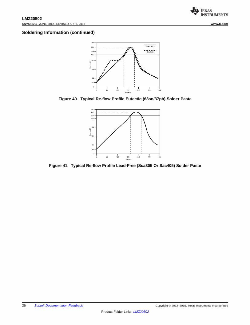
In addition, please follow the important guidelines found in: SNOA401. The curves in Figure 40 and Figure 41show typical soldering temperature profiles.
Copyright © 2012–2015, Texas Instruments Incorporated Submit Documentation Feedback 25
Product Folder Links: LMZ20502
LMZ20502SNVS852C –JUNE 2012–REVISED APRIL 2015 www.ti.com
Soldering Information (continued)
Figure 40. Typical Re-flow Profile Eutectic (63sn/37pb) Solder Paste
Figure 41. Typical Re-flow Profile Lead-Free (Sca305 Or Sac405) Solder Paste
26 Submit Documentation Feedback Copyright © 2012–2015, Texas Instruments Incorporated
Product Folder Links: LMZ20502

LMZ20502www.ti.com SNVS852C –JUNE 2012–REVISED APRIL 2015
12 Device and Documentation Support
12.1 Device Support
12.1.1 Third-Party Products DisclaimerTI'S PUBLICATION OF INFORMATION REGARDING THIRD-PARTY PRODUCTS OR SERVICES DOES NOTCONSTITUTE AN ENDORSEMENT REGARDING THE SUITABILITY OF SUCH PRODUCTS OR SERVICESOR A WARRANTY, REPRESENTATION OR ENDORSEMENT OF SUCH PRODUCTS OR SERVICES, EITHERALONE OR IN COMBINATION WITH ANY TI PRODUCT OR SERVICE.
12.1.2 Related LinksFor more information about Texas Instruments Simple Switcher product line, please visit our Simple Switcherpage: Simple Switcher.
Table 3. Resources For Estimating RθJA
TITLE LINKAN-2020 Thermal Design By Insight, Not SNVA419Hindsight
AN-2026 The Effect of PCB Design on theThermal Performance of SIMPLE SNVA424
SWITCHER Power ModulesAN-1520 A Guide to Board Layout for Best SNVA183Thermal Resistance for Exposed Packages
AN-1187 Leadless Lead-frame Package SNOA401(LLP)SPRA953B Semiconductor and IC Package SPRA953Thermal Metrics
Table 4. PCB Layout ResourcesTITLE LINK
AN-1149 Layout Guidelines for Switching SNVA021Power SuppliesAN-1229 SIMPLE SWITCHER PCB Layout SNVA054GuidelinesConstructing Your Power Supply- Layout SLUP230Considerations
12.2 TrademarksWebTherm is a trademark of Texas Instruments.SIMPLE SWITCHER, WEBENCH are registered trademarks of Texas Instruments.All other trademarks are the property of their respective owners.
12.3 Electrostatic Discharge CautionThese devices have limited built-in ESD protection. The leads should be shorted together or the device placed in conductive foamduring storage or handling to prevent electrostatic damage to the MOS gates.
12.4 GlossarySLYZ022 — TI Glossary.
This glossary lists and explains terms, acronyms, and definitions.
Copyright © 2012–2015, Texas Instruments Incorporated Submit Documentation Feedback 27
Product Folder Links: LMZ20502

LMZ20502SNVS852C –JUNE 2012–REVISED APRIL 2015 www.ti.com
13 Mechanical, Packaging, and Orderable InformationThe following pages include mechanical, packaging, and orderable information. This information is the mostcurrent data available for the designated devices. This data is subject to change without notice and revision ofthis document. For browser-based versions of this data sheet, refer to the left-hand navigation.
28 Submit Documentation Feedback Copyright © 2012–2015, Texas Instruments Incorporated
Product Folder Links: LMZ20502

www.ti.com
PACKAGE OUTLINE
C
B 3.5±0.1 A
3.5±0.1
(45 X0.25)PIN 1 ID
2X2.4
6X 0.8
(0.05) TYP
8X 0.50.3
8X 0.550.35
1.75 MAX
4X 0.8 0.1
8X 1.475 4X 0.55
4X 0.55
(2.5)
(2)
MicroSiP - 1.75 mm max heightSIL0008FMICRO SYSTEM IN PACKAGE
4221559/B 11/2014
PIN 1 INDEXAREA
PICK AREANOTE 3
0.08 C
0.1 C A B0.05 C
1
4 5
8
SYMM
SYMM
NOTES: 1. All linear dimensions are in millimeters. Any dimensions in parenthesis are for reference only. Dimensioning and tolerancing per ASME Y14.5M.2. This drawing is subject to change without notice. 3. Pick and place nozzle 1.3 mm or smaller recommended.
MicroSiP is a trademark of Texas Instruments.
TM
SCALE 3.800

www.ti.com
EXAMPLE BOARD LAYOUT
8X (0.45)
0.07 MAXALL AROUND
0.07 MINALL AROUND
8X (0.4)
(2.95)
6X (0.8)
4X (0.8)
(0.55) TYP
(0.55) TYP
MicroSiP - 1.75 mm max heightSIL0008FMICRO SYSTEM IN PACKAGE
4221559/B 11/2014
SYMM
SYMM
1
4 5
8
LAND PATTERN EXAMPLE1:1 RATIO WITH PACKAGE SOLDER PADS
SCALE:20X
NOTES: (continued) 4. This package is designed to be soldered to a thermal pad on the board. For more information, see Texas Instruments literature number SLUA271 (www.ti.com/lit/slua271).
TM
METAL
SOLDER MASKOPENING
NON SOLDER MASKDEFINED
SOLDER MASK DETAILSNOT TO SCALE
METAL UNDERSOLDER MASK
SOLDER MASKOPENING
SOLDER MASKDEFINED

www.ti.com
EXAMPLE STENCIL DESIGN
(0.55) TYP
(0.55) TYP
8X (0.4)
8X (0.45)
6X (0.8)
(2.95)
( 0.76)
MicroSiP - 1.75 mm max heightSIL0008FMICRO SYSTEM IN PACKAGE
4221559/B 11/2014
NOTES: (continued) 5. Laser cutting apertures with trapezoidal walls and rounded corners may offer better paste release. IPC-7525 may have alternate design recommendations.
TM
1
45
8
SYMM
SYMM
SOLDER PASTE EXAMPLEBASED ON 0.125 mm THICK STENCIL
EXPOSED PAD
90% PRINTED SOLDER COVERAGE BY AREASCALE:20X
SEE DETAIL
METALALL AROUND
DETAIL4 PLACES

LMZ20502www.ti.com SNVS852C –JUNE 2012–REVISED APRIL 2015
13.1 Package Option Addendum
13.1.1 Packaging Information
Package Package PackageOrderable Device Status (1) Pins Eco Plan (2) Lead/Ball Finish MSL Peak Temp (3) Op Temp (°C) Device Marking (4) (5)Type Drawing Qty
Green (RoHSLM20502SILR ACTIVE uSiP SIL 8 3000 Call TI Level-3-260C-168 HR -40 to 125 0502 7543 EC& no Sb/Br)
Green (RoHSLM20502SILT ACTIVE uSiP SIL 8 250 Call TI Level-3-260C-168 HR -40 to 125 0502 7543 EC& no Sb/Br)
(1) The marketing status values are defined as follows:ACTIVE: Product device recommended for new designs.LIFEBUY: TI has announced that the device will be discontinued, and a lifetime-buy period is in effect.NRND: Not recommended for new designs. Device is in production to support existing customers, but TI does not recommend using this part in a new design.PRE_PROD Unannounced device, not in production, not available for mass market, nor on the web, samples not available.PREVIEW: Device has been announced but is not in production. Samples may or may not be available.OBSOLETE: TI has discontinued the production of the device.space
(2) Eco Plan - The planned eco-friendly classification: Pb-Free (RoHS), Pb-Free (RoHS Exempt), or Green (RoHS & no Sb/Br) - please check http://www.ti.com/productcontent for the latestavailability information and additional product content details.TBD: The Pb-Free/Green conversion plan has not been defined.Pb-Free (RoHS): TI's terms "Lead-Free" or "Pb-Free" mean semiconductor products that are compatible with the current RoHS requirements for all 6 substances, including therequirement that lead not exceed 0.1% by weight in homogeneous materials. Where designed to be soldered at high temperatures, TI Pb-Free products are suitable for use in specifiedlead-free processes.Pb-Free (RoHS Exempt): This component has a RoHS exemption for either 1) lead-based flip-chip solder bumps used between the die and package, or 2) lead-based die adhesive usedbetween the die and leadframe. The component is otherwise considered Pb-Free (RoHS compatible) as defined above.Green (RoHS & no Sb/Br): TI defines "Green" to mean Pb-Free (RoHS compatible), and free of Bromine (Br) and Antimony (Sb) based flame retardants (Br or Sb do not exceed 0.1% byweight in homogeneous material)space
(3) MSL, Peak Temp. -- The Moisture Sensitivity Level rating according to the JEDEC industry standard classifications, and peak solder temperature.space
(4) There may be additional marking, which relates to the logo, the lot trace code information, or the environmental category on the devicespace
(5) Multiple Device markings will be inside parentheses. Only on Device Marking contained in parentheses and separated by a "~" will appear on a device. If a line is indented then it is acontinuation of the previous line and the two combined represent the entire Device Marking for that device.
Important Information and Disclaimer: The information provided on this page represents TI's knowledge and belief as of the date that it is provided. TI bases its knowledge and beliefon information provided by third parties, and makes no representation or warranty as to the accuracy of such information. Efforts are underway to better integrate information from thirdparties. TI has taken and continues to take reasonable steps to provide representative and accurate information but may not have conducted destructive testing or chemical analysis onincoming materials and chemicals. TI and TI suppliers consider certain information to be proprietary, and thus CAS numbers and other limited information may not be available forrelease.In no event shall TI's liability arising out of such information exceed the total purchase price of the TI part(s) at issue in this document sold by TI to Customer on an annual basis.
Copyright © 2012–2015, Texas Instruments Incorporated Submit Documentation Feedback 29
Product Folder Links: LMZ20502

PACKAGE OPTION ADDENDUM
www.ti.com 25-Oct-2016
Addendum-Page 1
PACKAGING INFORMATION
Orderable Device Status(1)
Package Type PackageDrawing
Pins PackageQty
Eco Plan(2)
Lead/Ball Finish(6)
MSL Peak Temp(3)
Op Temp (°C) Device Marking(4/5)
Samples
LMZ20502SILR ACTIVE uSiP SIL 8 3000 Green (RoHS& no Sb/Br)
Call TI Level-3-260C-168 HR -40 to 125 TXN5201ECEC754305020502 7543 EC
LMZ20502SILT ACTIVE uSiP SIL 8 250 Green (RoHS& no Sb/Br)
Call TI Level-3-260C-168 HR -40 to 125 TXN5201ECEC754305020502 7543 EC
(1) The marketing status values are defined as follows:ACTIVE: Product device recommended for new designs.LIFEBUY: TI has announced that the device will be discontinued, and a lifetime-buy period is in effect.NRND: Not recommended for new designs. Device is in production to support existing customers, but TI does not recommend using this part in a new design.PREVIEW: Device has been announced but is not in production. Samples may or may not be available.OBSOLETE: TI has discontinued the production of the device.
(2) Eco Plan - The planned eco-friendly classification: Pb-Free (RoHS), Pb-Free (RoHS Exempt), or Green (RoHS & no Sb/Br) - please check http://www.ti.com/productcontent for the latest availabilityinformation and additional product content details.TBD: The Pb-Free/Green conversion plan has not been defined.Pb-Free (RoHS): TI's terms "Lead-Free" or "Pb-Free" mean semiconductor products that are compatible with the current RoHS requirements for all 6 substances, including the requirement thatlead not exceed 0.1% by weight in homogeneous materials. Where designed to be soldered at high temperatures, TI Pb-Free products are suitable for use in specified lead-free processes.Pb-Free (RoHS Exempt): This component has a RoHS exemption for either 1) lead-based flip-chip solder bumps used between the die and package, or 2) lead-based die adhesive used betweenthe die and leadframe. The component is otherwise considered Pb-Free (RoHS compatible) as defined above.Green (RoHS & no Sb/Br): TI defines "Green" to mean Pb-Free (RoHS compatible), and free of Bromine (Br) and Antimony (Sb) based flame retardants (Br or Sb do not exceed 0.1% by weightin homogeneous material)
(3) MSL, Peak Temp. - The Moisture Sensitivity Level rating according to the JEDEC industry standard classifications, and peak solder temperature.
(4) There may be additional marking, which relates to the logo, the lot trace code information, or the environmental category on the device.
(5) Multiple Device Markings will be inside parentheses. Only one Device Marking contained in parentheses and separated by a "~" will appear on a device. If a line is indented then it is a continuationof the previous line and the two combined represent the entire Device Marking for that device.
(6) Lead/Ball Finish - Orderable Devices may have multiple material finish options. Finish options are separated by a vertical ruled line. Lead/Ball Finish values may wrap to two lines if the finishvalue exceeds the maximum column width.

PACKAGE OPTION ADDENDUM
www.ti.com 25-Oct-2016
Addendum-Page 2
Important Information and Disclaimer:The information provided on this page represents TI's knowledge and belief as of the date that it is provided. TI bases its knowledge and belief on informationprovided by third parties, and makes no representation or warranty as to the accuracy of such information. Efforts are underway to better integrate information from third parties. TI has taken andcontinues to take reasonable steps to provide representative and accurate information but may not have conducted destructive testing or chemical analysis on incoming materials and chemicals.TI and TI suppliers consider certain information to be proprietary, and thus CAS numbers and other limited information may not be available for release.
In no event shall TI's liability arising out of such information exceed the total purchase price of the TI part(s) at issue in this document sold by TI to Customer on an annual basis.

IMPORTANT NOTICE
Texas Instruments Incorporated (TI) reserves the right to make corrections, enhancements, improvements and other changes to itssemiconductor products and services per JESD46, latest issue, and to discontinue any product or service per JESD48, latest issue. Buyersshould obtain the latest relevant information before placing orders and should verify that such information is current and complete.TI’s published terms of sale for semiconductor products (http://www.ti.com/sc/docs/stdterms.htm) apply to the sale of packaged integratedcircuit products that TI has qualified and released to market. Additional terms may apply to the use or sale of other types of TI products andservices.Reproduction of significant portions of TI information in TI data sheets is permissible only if reproduction is without alteration and isaccompanied by all associated warranties, conditions, limitations, and notices. TI is not responsible or liable for such reproduceddocumentation. Information of third parties may be subject to additional restrictions. Resale of TI products or services with statementsdifferent from or beyond the parameters stated by TI for that product or service voids all express and any implied warranties for theassociated TI product or service and is an unfair and deceptive business practice. TI is not responsible or liable for any such statements.Buyers and others who are developing systems that incorporate TI products (collectively, “Designers”) understand and agree that Designersremain responsible for using their independent analysis, evaluation and judgment in designing their applications and that Designers havefull and exclusive responsibility to assure the safety of Designers' applications and compliance of their applications (and of all TI productsused in or for Designers’ applications) with all applicable regulations, laws and other applicable requirements. Designer represents that, withrespect to their applications, Designer has all the necessary expertise to create and implement safeguards that (1) anticipate dangerousconsequences of failures, (2) monitor failures and their consequences, and (3) lessen the likelihood of failures that might cause harm andtake appropriate actions. Designer agrees that prior to using or distributing any applications that include TI products, Designer willthoroughly test such applications and the functionality of such TI products as used in such applications.TI’s provision of technical, application or other design advice, quality characterization, reliability data or other services or information,including, but not limited to, reference designs and materials relating to evaluation modules, (collectively, “TI Resources”) are intended toassist designers who are developing applications that incorporate TI products; by downloading, accessing or using TI Resources in anyway, Designer (individually or, if Designer is acting on behalf of a company, Designer’s company) agrees to use any particular TI Resourcesolely for this purpose and subject to the terms of this Notice.TI’s provision of TI Resources does not expand or otherwise alter TI’s applicable published warranties or warranty disclaimers for TIproducts, and no additional obligations or liabilities arise from TI providing such TI Resources. TI reserves the right to make corrections,enhancements, improvements and other changes to its TI Resources. TI has not conducted any testing other than that specificallydescribed in the published documentation for a particular TI Resource.Designer is authorized to use, copy and modify any individual TI Resource only in connection with the development of applications thatinclude the TI product(s) identified in such TI Resource. NO OTHER LICENSE, EXPRESS OR IMPLIED, BY ESTOPPEL OR OTHERWISETO ANY OTHER TI INTELLECTUAL PROPERTY RIGHT, AND NO LICENSE TO ANY TECHNOLOGY OR INTELLECTUAL PROPERTYRIGHT OF TI OR ANY THIRD PARTY IS GRANTED HEREIN, including but not limited to any patent right, copyright, mask work right, orother intellectual property right relating to any combination, machine, or process in which TI products or services are used. Informationregarding or referencing third-party products or services does not constitute a license to use such products or services, or a warranty orendorsement thereof. Use of TI Resources may require a license from a third party under the patents or other intellectual property of thethird party, or a license from TI under the patents or other intellectual property of TI.TI RESOURCES ARE PROVIDED “AS IS” AND WITH ALL FAULTS. TI DISCLAIMS ALL OTHER WARRANTIES ORREPRESENTATIONS, EXPRESS OR IMPLIED, REGARDING RESOURCES OR USE THEREOF, INCLUDING BUT NOT LIMITED TOACCURACY OR COMPLETENESS, TITLE, ANY EPIDEMIC FAILURE WARRANTY AND ANY IMPLIED WARRANTIES OFMERCHANTABILITY, FITNESS FOR A PARTICULAR PURPOSE, AND NON-INFRINGEMENT OF ANY THIRD PARTY INTELLECTUALPROPERTY RIGHTS. TI SHALL NOT BE LIABLE FOR AND SHALL NOT DEFEND OR INDEMNIFY DESIGNER AGAINST ANY CLAIM,INCLUDING BUT NOT LIMITED TO ANY INFRINGEMENT CLAIM THAT RELATES TO OR IS BASED ON ANY COMBINATION OFPRODUCTS EVEN IF DESCRIBED IN TI RESOURCES OR OTHERWISE. IN NO EVENT SHALL TI BE LIABLE FOR ANY ACTUAL,DIRECT, SPECIAL, COLLATERAL, INDIRECT, PUNITIVE, INCIDENTAL, CONSEQUENTIAL OR EXEMPLARY DAMAGES INCONNECTION WITH OR ARISING OUT OF TI RESOURCES OR USE THEREOF, AND REGARDLESS OF WHETHER TI HAS BEENADVISED OF THE POSSIBILITY OF SUCH DAMAGES.Unless TI has explicitly designated an individual product as meeting the requirements of a particular industry standard (e.g., ISO/TS 16949and ISO 26262), TI is not responsible for any failure to meet such industry standard requirements.Where TI specifically promotes products as facilitating functional safety or as compliant with industry functional safety standards, suchproducts are intended to help enable customers to design and create their own applications that meet applicable functional safety standardsand requirements. Using products in an application does not by itself establish any safety features in the application. Designers mustensure compliance with safety-related requirements and standards applicable to their applications. Designer may not use any TI products inlife-critical medical equipment unless authorized officers of the parties have executed a special contract specifically governing such use.Life-critical medical equipment is medical equipment where failure of such equipment would cause serious bodily injury or death (e.g., lifesupport, pacemakers, defibrillators, heart pumps, neurostimulators, and implantables). Such equipment includes, without limitation, allmedical devices identified by the U.S. Food and Drug Administration as Class III devices and equivalent classifications outside the U.S.TI may expressly designate certain products as completing a particular qualification (e.g., Q100, Military Grade, or Enhanced Product).Designers agree that it has the necessary expertise to select the product with the appropriate qualification designation for their applicationsand that proper product selection is at Designers’ own risk. Designers are solely responsible for compliance with all legal and regulatoryrequirements in connection with such selection.Designer will fully indemnify TI and its representatives against any damages, costs, losses, and/or liabilities arising out of Designer’s non-compliance with the terms and provisions of this Notice.
Mailing Address: Texas Instruments, Post Office Box 655303, Dallas, Texas 75265Copyright © 2017, Texas Instruments Incorporated