lms4684 0.5Ωlow-voltage,dual spdt analog switch
TRANSCRIPT

NO1
COM1
IN1
COM2
1
4
5
3
7
6
8
10
GND
NO2
IN2
2 9
NC1
NC2
GND
V+
NO1 COM1 IN1
V+ GND
NO2 COM2 IN2
C2
D3
D2
D1
A3 B3 C3
A2 B2
A1 B1 C1
NC1
NC2
LMS4684
www.ti.com SNOSAL0C –DECEMBER 2004–REVISED APRIL 2013
LMS4684 0.5Ω Low-Voltage, Dual SPDT Analog SwitchCheck for Samples: LMS4684
1FEATURES DESCRIPTIONThe LMS4684 is a low on-resistance, low voltage
2• NC Switch RON 0.5Ω max @ 2.7Vdual SPDT (Single-Pole/Double-Throw) analog switch
• NO Switch RON 0.8Ω max @ 2.7V that operates from a 1.8V to 5.5V supply. The• 5 nA (typ) Supply Current TA = 25°C LMS4684 features a 0.5Ω RON for its NC switch and
0.8Ω RON for its NO switch at a 2.7V supply. The• 1.8 to 5.5V Single Supply Operationdigital logic inputs are 1.8V logic-compatible with a• 12-Bump DSBGA Package 2.7V to 3.3V supply and features break-before-make
• WSON-10 Package, 3x4mm switching action.
The LMS4684 is available in the 12-bump DSBGAAPPLICATIONSand the 10-lead WSON miniature packages. These
• Power Routing PCB real estate saving packages offer extremeperformance while saving money with small• Battery-Operated Equipmentfootprints.• Communications Circuits
• Modems• Cell Phones
Connection Diagram
Center Bumps B2 and C2 are Not Electrically Connected
Exposed pad on back of package needs to be connected to pin 6 onthe board
Figure 1. 10-WSON Package-Top View Figure 2. 12-Bump DSBGA Package-Top View(Bumped Side Down)
1
Please be aware that an important notice concerning availability, standard warranty, and use in critical applications ofTexas Instruments semiconductor products and disclaimers thereto appears at the end of this data sheet.
2All trademarks are the property of their respective owners.
PRODUCTION DATA information is current as of publication date. Copyright © 2004–2013, Texas Instruments IncorporatedProducts conform to specifications per the terms of the TexasInstruments standard warranty. Production processing does notnecessarily include testing of all parameters.

NO1
COM1
IN1
COM2
1
4
5
3
7
6
8
10 NO2
IN2
2 9
NC1
NC2
GND
V+
LMS4684
SNOSAL0C –DECEMBER 2004–REVISED APRIL 2013 www.ti.com
SCHEMATIC DIAGRAM
IN NO NC
0 Off On
1 On Off
Switches shown for Logic "0" input
PIN DESCRIPTIONSName Pin ID Description
WSON DSBGA
NC 5, 7 D3, D1 Analog switch normally closed terminal
IN 4, 8 C3, C1 Digital control input
COM 3, 9 B3, B1 Analog switch common terminal
NO 2, 10 A3, A1 Analog switch normally open terminal
V+ 1 A2 Positive supply voltage
GND 6 D2 Ground
Not electrically connected. Can be used to help dissipate heat by connecting to GNDB2, C2 pin.
These devices have limited built-in ESD protection. The leads should be shorted together or the device placed in conductive foamduring storage or handling to prevent electrostatic damage to the MOS gates.
ABSOLUTE MAXIMUM RATINGS (1) (2) (3)
V+ −0.3V to 6.0V
IN −0.3V to 6.0V
COM, NO, NC −0.3V to (V+ + 0.3V)
Continuous Switch Current ±400 mA
ESD Tolerance (4) Human Body Model 2000V
Machine Model 200V
Storage Temperature Range −65°C to 150°C
Junction Temperature (5) 150°C Max
(1) Absolute Maximum Ratings indicate limits beyond which damage to the device may occur. Operating Ratings indicate conditions forwhich the device is intended to be functional, but specific performance is not guaranteed.
(2) All voltages are with respect to GND, unless otherwise specified.(3) If Military/Aerospace specified devices are required, please contact the Texas Instruments Sales Office/ Distributors for availability and
specifications.(4) Human body model: 1.5 kΩ in series with 100 pF. Machine model, 0Ω in series with 200 pF.(5) The maximum power dissipation is a function of TJ(max), θJA and TA.
2 Submit Documentation Feedback Copyright © 2004–2013, Texas Instruments Incorporated
Product Folder Links: LMS4684

LMS4684
www.ti.com SNOSAL0C –DECEMBER 2004–REVISED APRIL 2013
OPERATING RATINGSNominal Supply Voltage 1.8V to 5.5V
IN Voltage (regardless of supply) −0.3V to 5.5V
Temperature Range −40°C to 85°C
(1) Absolute Maximum Ratings indicate limits beyond which damage to the device may occur. Operating Ratings indicate conditions forwhich the device is intended to be functional, but specific performance is not guaranteed.
(2) All voltages are with respect to GND, unless otherwise specified.
PACKAGE THERMAL RESISTANCEPackage θJ-A
WSON-10 43°C / W
DSBGA-12 57°C / W
ELECTRICAL CHARACTERISTICSUnless otherwise specified, V+ = 2.7 to 3.3V, VIH = 1.4V, VIL = 0.5V. Typical values are measured at 3V, and TJ = 25°C.Boldface limits apply at temperature extremes.
Symbol Parameter Conditions Min Typ Max Units
VNO, VNC, VCOM Analog Signal Range 0 V+ V
V+ = 2.7V, ICOM = 100 mA,RON (NC) NC On-Resistance (1) 0.3 0.5 ΩVNC =0 to V+
NO On-Resistance V+ = 2.7V, ICOM = 100 mA,RON (NO) 0.45 0.8 Ω(1) VNO =0 to V+
On-Resistance Match V+ = 2.7V, ICOM = 100 mA,ΔRON 1.11 60 mΩBetween Channels (1), (2) VNC or VNO =1.5V
WSONTJ = -40°C to 0.1 0.25
V+ = 2.7V, 85°CNC-On-ResistanceRFLAT(NC) ICOM = 100 mA, ΩFlatness (3)DSBGAVNC = 0 to V+
TJ = -40°C to 0.1 0.2585°C
NO On-Resistance V+ = 2.7V, ICOM = 100 mA,RFLAT(NO) 0.18 0.35 ΩFlatness (3) VNO = 0 to V+
−1 0.014 1NO or NC Off Leakage V+ = 3.3V, VNO or VNC = 3V,INO(OFF) or INC(OFF) nACurrent 0.3V; VCOM = 0.3V, 3V −10 10
V+ = 3.3V, VNO or VNC = 3V, −2 2ICOM (ON) COM On Leakage Current 0.3V, or floating; VCOM = 3V, or nA
−20 20floating
Dynamic Characteristics
38 60V+ = 2.7V, VNO or VNC = 1.5V;tON Turn-On Time nsRL = 50Ω; CL = 35 pF; 70
22 40V+ = 2.7V, VNO or VNC = 1.5V;tOFF Turn-Off Time nsRL = 50Ω; CL = 35 pF; 50
V+ = 2.7V, VNO or VNC = 1.5V;tBBM Break-Before-Make Delay 2 15 nsRL = 50Ω; CL = 35 pF;
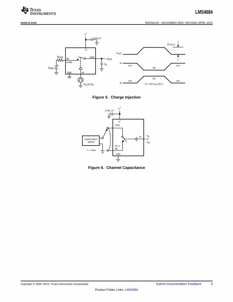
Q Charge Injection COM = 0; RS = 0; CL= 1 nF; 200 pC
VISO Off-Isolation (4) RL = 50Ω; CL= 5 pF; f = 100 kHz -68 dB
VCT Crosstalk -72 dB
Digital I/O
VIH Input Logic High 1.4 V
VIL Input Logic Low 0.5 V
(1) Guaranteed by design.(2) ΔRON is equal to the difference between NC1/NC2 RON or NO1/NO2 RON at a specified voltage.(3) Flatness is defined as the difference between the maximum and minimum value of on-resistance as measured over the specified analog
signal ranges.(4) Off-isolation = 20 log10(VCOM/ VNO), where VCOM = output, VNO = input switch off.
Copyright © 2004–2013, Texas Instruments Incorporated Submit Documentation Feedback 3
Product Folder Links: LMS4684

0.9 x VOUT
50%
VIH
VIL
LOGIC
INPUT
tD
GNDLOGIC
INPUT
V+
NO
NC
IN
CL INCLUDES FIXTURE AND STRAY CAPACITANCE
COM
VOUT
RL50:
CL 100pF
VIN
V+
0.047PF
50%
VIH
VIL
LOGIC
INPUT
0.9 x VOUTSWITCH
OUPUT
VOUT
0
tOFF
tON
0.9 x VOUT
VOUT
RL50:
VIN
V+
GNDLOGIC
INPUT
CL 100pF
NO
or NC
IN
CL INCLUDES FIXTURE AND STRAY CAPACITANCE
V+
COM
0.047PF
LMS4684
SNOSAL0C –DECEMBER 2004–REVISED APRIL 2013 www.ti.com
ELECTRICAL CHARACTERISTICS (continued)Unless otherwise specified, V+ = 2.7 to 3.3V, VIH = 1.4V, VIL = 0.5V. Typical values are measured at 3V, and TJ = 25°C.Boldface limits apply at temperature extremes.
Symbol Parameter Conditions Min Typ Max Units
IIN IN Input Leakage Current VIN = 0 or V+ −1 1 μA
Power Supply
V+ Power-Supply Range 1.8 5.5 V
I+ Supply Current V+ = 5.5V 5 nA
PARAMETRIC MEASUREMENT INFORMATION
Figure 3. tON / tOFF Time
Figure 4. Break-Before Make Delay
4 Submit Documentation Feedback Copyright © 2004–2013, Texas Instruments Incorporated
Product Folder Links: LMS4684
CAPACITANCE
METER
f = 1 MHz
COM
V+
V+
GND
IN
0.047 PF
NC or
NO
VIL or
VIH
VOUT
IN
IN
OFF
ON
OFF OFF
OFF
ON
Q = ( VOUT)(CL)
VOUT
V+
or NO
NC
IN
COMVOUT
CL
GND
VIL to VIH
RGEN
VGEN
+
V+
0.047PF
LMS4684
www.ti.com SNOSAL0C –DECEMBER 2004–REVISED APRIL 2013
Figure 5. Charge Injection
Figure 6. Channel Capacitance
Copyright © 2004–2013, Texas Instruments Incorporated Submit Documentation Feedback 5
Product Folder Links: LMS4684

0 1 2 3 4 5 6
VSUPPLY (V)
0
0.5
1
1.5
2
LOG
IC T
HR
ES
HO
LD V
OLT
AG
E (
V)
VIN RISING
VIN FALLING
-40 -15 10 35 60 850
5
10
15
20
25
30
35
40
45
50
t ON
, t O
FF
(ns)
TEMPERATURE
V+ = 3V
CL = 100 pF
RL = 50:
tON (ns)
tOFF (ns)
0 1 2 3 4 50.0
0.5
1.0
1.5
2.0
2.5
3.0
RO
N (:
)
VCOM (V)
V+ = 1.8V
V+ = 2.0V
V+ = 2.3V
V+ = 2.5V
V+ = 3.0V
V+ = 5.0V
0.0 1.0 2.0 3.0 4.0 5.00.00
0.25
0.50
0.75
1.00
1.25
1.50
1.75
2.00
2.25
2.50
RO
N (:
)
VCOM (V)
VS = 2.3V
VS = 2.5V
VS = 2.0V
VS = 3.0V
VS = 1.8V
VS = 5.0V
LMS4684
SNOSAL0C –DECEMBER 2004–REVISED APRIL 2013 www.ti.com
TYPICAL PERFORMANCE CHARACTERISTICS
NO ON Resistance NC ON Resistancevs. vs.
COM Voltage COM Voltage
Figure 7. Figure 8.
Logic Threshold Voltage Turn-on / Turn-off Timesvs. vs.
Supply Voltage Temperature
Figure 9. Figure 10.
6 Submit Documentation Feedback Copyright © 2004–2013, Texas Instruments Incorporated
Product Folder Links: LMS4684

0 1 2 3 4 50.10
0.15
0.20
0.25
0.30
0.35
0.40
RO
N (:
)
VCOM (V)
V+ = 5V
TA = +85ºC
TA = +25ºC
TA = -40ºC
0 0.5 1 1.5 2 2.5 30.10
0.15
0.20
0.25
0.30
0.35
0.40
0.45
0.50
0.55
0.60
RO
N (:
)
VCOM (V)
V+ = 3VTA = +85ºC
TA = +25ºC
TA = -40ºC
0 0.5 1 1.5 2 2.5 3
VCOM (V)
0.10
0.15
0.20
0.25
0.30
0.35
RO
N (:
)
V+ = 3V
TA = +85ºC
TA = +25ºC
TA = -40ºC
0 1 2 3 4 5 6
VCOM (V)
-700
-500
-300
-100
100
300
500
Q (
pC)
0 1 2 3 4 50.10
0.12
0.14
0.16
0.18
0.20
0.22
0.24
0.26
0.28
0.30
RO
N (:
)
VCOM (V)
V+ = 5V
TA = +85ºC
TA = +25ºC
TA = -40ºC
LMS4684
www.ti.com SNOSAL0C –DECEMBER 2004–REVISED APRIL 2013
TYPICAL PERFORMANCE CHARACTERISTICS (continued)Charge Injection NC On-Resistance
vs. vs.COM Voltage COM Voltage
Figure 11. Figure 12.
NC On-Resistance NO On-Resistancevs. vs.
COM Voltage COM Voltage
Figure 13. Figure 14.
NO On-Resistancevs.
COM Voltage
Figure 15.
Copyright © 2004–2013, Texas Instruments Incorporated Submit Documentation Feedback 7
Product Folder Links: LMS4684

V+
or NO
NC
IN
COMVOUT
GND
VIL to VIH
VIN
+
V+
0.047PF
Protection
Diode
Motor or
inductive
load
LMS4684
SNOSAL0C –DECEMBER 2004–REVISED APRIL 2013 www.ti.com
FUNCTIONAL DESCRIPTION
The LMS4684 is a low voltage dual, extremely low On-Resistance analog switch that can operate over a supplyvoltage range of 1.8V to 5.5V. The LMS4684 has been fully characterized to operate in applications with 3Vnominal supply voltage and features very low on resistance and fast Turn-Off and Turn-On times with break-before-make switching.
The switch operates asymmetrically; one terminal is normally closed (NC) and the other terminal normally open(NO).
Both NC and NO terminals are connected to a common terminal (COM). This configuration is ideal forapplications with asymmetric loads such as speaker handsets and internal speakers.
Applications Information
ANALOG INPUT SIGNAL
Analog input signals can range from GND to V+ and are passed through the switch with very little change. Eachswitch is bidirectional so any pin can be an input or output.
Exercise care when making connection to an inductive load, such as a motor. As is true with any analog switchused with an inductive load, the back emf produced when the switch is turned off can damage the LMS4684 byelectrical overstress. For such applications, a diode should be connected across the motor to prevent damage tothe switch, as indicated in Figure 16. Be sure the diode has adequate current carrying capabilities.
Figure 16. Inductive Load Over-Voltage Protection
DIGITAL CONTROL INPUTS
The IN pin can be driven to 5.5V regardless of the voltage level of the supply pin V+. For example, if theLMS4684 is operated with a supply of 2V, the digital control input could still be driven to 5V. Power consumptionis increased when the control pin is driven rail-to-rail.
SUPPLY VOLTAGE
It is good general practice to first apply the supply voltage to a CMOS device before sriving any other pins. Thisis also true for the LMS4684 analog switch, which is a CMOS device.
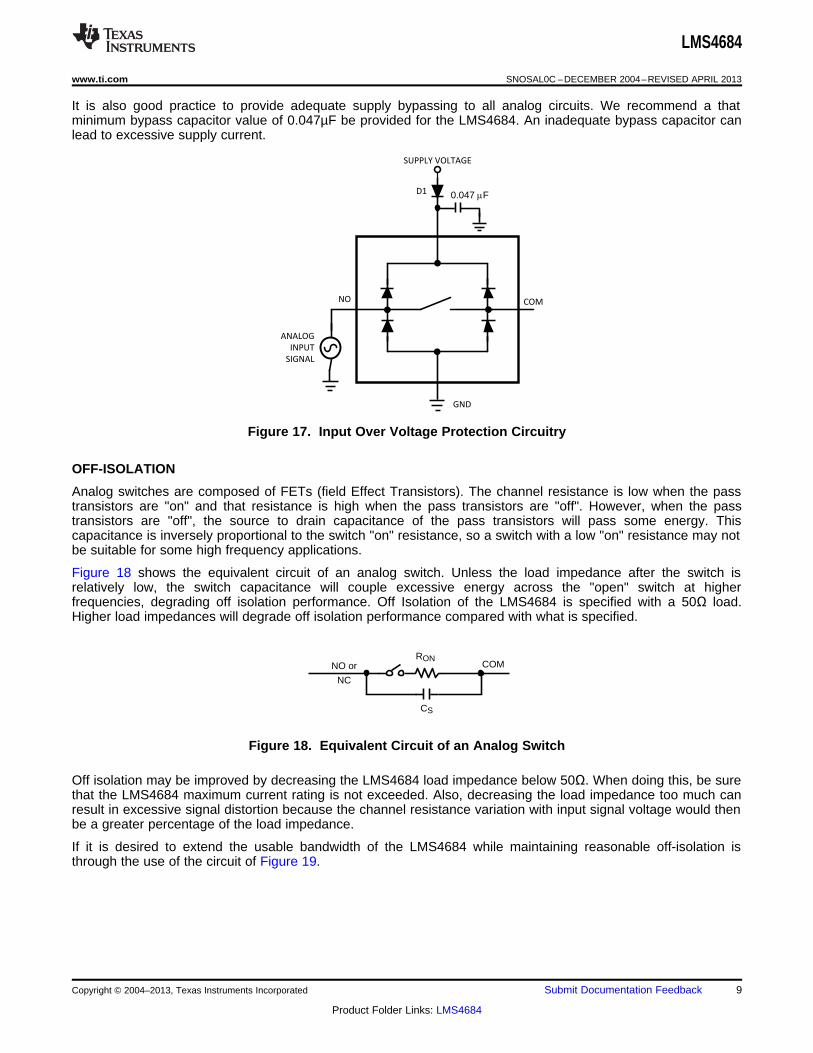
However, if it is necessary to have an analog signal applied before the supply voltage is applied and the analogsignal source is not limited to 20 mA max, a diode connected between the supply voltage and the V+ pin asshown in Figure 17 will provide input protection. This will limit the max analog voltage to a diode drop below V+.This diode, D1, will also provide protection against some over voltage situations.
8 Submit Documentation Feedback Copyright © 2004–2013, Texas Instruments Incorporated
Product Folder Links: LMS4684
RONCOMNO or
NC
CS
SUPPLY VOLTAGE
ANALOG
INPUT
SIGNAL
COM
D1
NO
GND
0.047 PF
LMS4684
www.ti.com SNOSAL0C –DECEMBER 2004–REVISED APRIL 2013
It is also good practice to provide adequate supply bypassing to all analog circuits. We recommend a thatminimum bypass capacitor value of 0.047µF be provided for the LMS4684. An inadequate bypass capacitor canlead to excessive supply current.
Figure 17. Input Over Voltage Protection Circuitry
OFF-ISOLATION
Analog switches are composed of FETs (field Effect Transistors). The channel resistance is low when the passtransistors are "on" and that resistance is high when the pass transistors are "off". However, when the passtransistors are "off", the source to drain capacitance of the pass transistors will pass some energy. Thiscapacitance is inversely proportional to the switch "on" resistance, so a switch with a low "on" resistance may notbe suitable for some high frequency applications.
Figure 18 shows the equivalent circuit of an analog switch. Unless the load impedance after the switch isrelatively low, the switch capacitance will couple excessive energy across the "open" switch at higherfrequencies, degrading off isolation performance. Off Isolation of the LMS4684 is specified with a 50Ω load.Higher load impedances will degrade off isolation performance compared with what is specified.
Figure 18. Equivalent Circuit of an Analog Switch
Off isolation may be improved by decreasing the LMS4684 load impedance below 50Ω. When doing this, be surethat the LMS4684 maximum current rating is not exceeded. Also, decreasing the load impedance too much canresult in excessive signal distortion because the channel resistance variation with input signal voltage would thenbe a greater percentage of the load impedance.
If it is desired to extend the usable bandwidth of the LMS4684 while maintaining reasonable off-isolation isthrough the use of the circuit of Figure 19.
Copyright © 2004–2013, Texas Instruments Incorporated Submit Documentation Feedback 9
Product Folder Links: LMS4684

VIN
V+
GND
NO
NC
V+
COM
0.047 PF
LMS4684
SNOSAL0C –DECEMBER 2004–REVISED APRIL 2013 www.ti.com
Figure 19. Using the LMS4684 at higher frequencies
PCB LAYOUT AND THERMAL CONSIDERATIONS
Both the WSON and DSBGA packages offer enhanced board real estate savings because of their smallfootprints. These tiny packages are capable of handling high continuous currents because of the advancedpackage thermal handling capabilities.
The WSON package has the exposed die attach pad internally connected to the internal circuit GND. When thispad is soldered to copper on the PCB board according to Application Note AN-1187, the full thermal capability ofthe WSON package can be achieved without additional bulky heat sinks to dissipate the heat generated. TheDSBGA package has a similar capability to dissipate heat through Bumps B2 and C2, which are not electricallyconnected. To enhance heat dissipation of the DSBGA package B2 and C2 could be connected to the GND pinthrough copper traces on the board.
See Application Note AN-1112 for DSBGA package considerations.
10 Submit Documentation Feedback Copyright © 2004–2013, Texas Instruments Incorporated
Product Folder Links: LMS4684

LMS4684
www.ti.com SNOSAL0C –DECEMBER 2004–REVISED APRIL 2013
REVISION HISTORY
Changes from Revision B (April 2013) to Revision C Page
• Changed layout of National Data Sheet to TI format .......................................................................................................... 10
Copyright © 2004–2013, Texas Instruments Incorporated Submit Documentation Feedback 11
Product Folder Links: LMS4684

PACKAGE OPTION ADDENDUM
www.ti.com 10-Dec-2020
Addendum-Page 1
PACKAGING INFORMATION
Orderable Device Status(1)
Package Type PackageDrawing
Pins PackageQty
Eco Plan(2)
Lead finish/Ball material
(6)
MSL Peak Temp(3)
Op Temp (°C) Device Marking(4/5)
Samples
LMS4684ITL/NOPB ACTIVE DSBGA YZR 12 250 RoHS & Green SNAGCU Level-1-260C-UNLIM -40 to 85 F09A
LMS4684ITLX/NOPB ACTIVE DSBGA YZR 12 3000 RoHS & Green SNAGCU Level-1-260C-UNLIM -40 to 85 F09A
LMS4684LD/NOPB ACTIVE WSON NGZ 10 1000 RoHS & Green SN Level-3-260C-168 HR -40 to 85 L4684
(1) The marketing status values are defined as follows:ACTIVE: Product device recommended for new designs.LIFEBUY: TI has announced that the device will be discontinued, and a lifetime-buy period is in effect.NRND: Not recommended for new designs. Device is in production to support existing customers, but TI does not recommend using this part in a new design.PREVIEW: Device has been announced but is not in production. Samples may or may not be available.OBSOLETE: TI has discontinued the production of the device.
(2) RoHS: TI defines "RoHS" to mean semiconductor products that are compliant with the current EU RoHS requirements for all 10 RoHS substances, including the requirement that RoHS substancedo not exceed 0.1% by weight in homogeneous materials. Where designed to be soldered at high temperatures, "RoHS" products are suitable for use in specified lead-free processes. TI mayreference these types of products as "Pb-Free".RoHS Exempt: TI defines "RoHS Exempt" to mean products that contain lead but are compliant with EU RoHS pursuant to a specific EU RoHS exemption.Green: TI defines "Green" to mean the content of Chlorine (Cl) and Bromine (Br) based flame retardants meet JS709B low halogen requirements of <=1000ppm threshold. Antimony trioxide basedflame retardants must also meet the <=1000ppm threshold requirement.
(3) MSL, Peak Temp. - The Moisture Sensitivity Level rating according to the JEDEC industry standard classifications, and peak solder temperature.
(4) There may be additional marking, which relates to the logo, the lot trace code information, or the environmental category on the device.
(5) Multiple Device Markings will be inside parentheses. Only one Device Marking contained in parentheses and separated by a "~" will appear on a device. If a line is indented then it is a continuationof the previous line and the two combined represent the entire Device Marking for that device.
(6) Lead finish/Ball material - Orderable Devices may have multiple material finish options. Finish options are separated by a vertical ruled line. Lead finish/Ball material values may wrap to twolines if the finish value exceeds the maximum column width.
Important Information and Disclaimer:The information provided on this page represents TI's knowledge and belief as of the date that it is provided. TI bases its knowledge and belief on informationprovided by third parties, and makes no representation or warranty as to the accuracy of such information. Efforts are underway to better integrate information from third parties. TI has taken andcontinues to take reasonable steps to provide representative and accurate information but may not have conducted destructive testing or chemical analysis on incoming materials and chemicals.TI and TI suppliers consider certain information to be proprietary, and thus CAS numbers and other limited information may not be available for release.

PACKAGE OPTION ADDENDUM
www.ti.com 10-Dec-2020
Addendum-Page 2
In no event shall TI's liability arising out of such information exceed the total purchase price of the TI part(s) at issue in this document sold by TI to Customer on an annual basis.

TAPE AND REEL INFORMATION
*All dimensions are nominal
Device PackageType
PackageDrawing
Pins SPQ ReelDiameter
(mm)
ReelWidth
W1 (mm)
A0(mm)
B0(mm)
K0(mm)
P1(mm)
W(mm)
Pin1Quadrant
LMS4684ITL/NOPB DSBGA YZR 12 250 178.0 8.4 1.73 2.46 0.76 4.0 8.0 Q1
LMS4684ITLX/NOPB DSBGA YZR 12 3000 178.0 8.4 1.73 2.46 0.76 4.0 8.0 Q1
LMS4684LD/NOPB WSON NGZ 10 1000 178.0 12.4 4.3 3.3 1.0 8.0 12.0 Q1
PACKAGE MATERIALS INFORMATION
www.ti.com 5-Nov-2021
Pack Materials-Page 1

*All dimensions are nominal
Device Package Type Package Drawing Pins SPQ Length (mm) Width (mm) Height (mm)
LMS4684ITL/NOPB DSBGA YZR 12 250 208.0 191.0 35.0
LMS4684ITLX/NOPB DSBGA YZR 12 3000 208.0 191.0 35.0
LMS4684LD/NOPB WSON NGZ 10 1000 208.0 191.0 35.0
PACKAGE MATERIALS INFORMATION
www.ti.com 5-Nov-2021
Pack Materials-Page 2

MECHANICAL DATA
NGZ0010B
www.ti.com
LDA10B (Rev B)

MECHANICAL DATA
YZR0012xxx
www.ti.com
TLA12XXX (Rev C)
0.600±0.075 D
E
A. All linear dimensions are in millimeters. Dimensioning and tolerancing per ASME Y14.5M-1994.B. This drawing is subject to change without notice.
4215049/A 12/12
NOTES:
D: Max =
E: Max =
2.378 mm, Min =
1.641 mm, Min =
2.317 mm
1.581 mm

IMPORTANT NOTICE AND DISCLAIMERTI PROVIDES TECHNICAL AND RELIABILITY DATA (INCLUDING DATA SHEETS), DESIGN RESOURCES (INCLUDING REFERENCE DESIGNS), APPLICATION OR OTHER DESIGN ADVICE, WEB TOOLS, SAFETY INFORMATION, AND OTHER RESOURCES “AS IS” AND WITH ALL FAULTS, AND DISCLAIMS ALL WARRANTIES, EXPRESS AND IMPLIED, INCLUDING WITHOUT LIMITATION ANY IMPLIED WARRANTIES OF MERCHANTABILITY, FITNESS FOR A PARTICULAR PURPOSE OR NON-INFRINGEMENT OF THIRD PARTY INTELLECTUAL PROPERTY RIGHTS.These resources are intended for skilled developers designing with TI products. You are solely responsible for (1) selecting the appropriate TI products for your application, (2) designing, validating and testing your application, and (3) ensuring your application meets applicable standards, and any other safety, security, regulatory or other requirements.These resources are subject to change without notice. TI grants you permission to use these resources only for development of an application that uses the TI products described in the resource. Other reproduction and display of these resources is prohibited. No license is granted to any other TI intellectual property right or to any third party intellectual property right. TI disclaims responsibility for, and you will fully indemnify TI and its representatives against, any claims, damages, costs, losses, and liabilities arising out of your use of these resources.TI’s products are provided subject to TI’s Terms of Sale or other applicable terms available either on ti.com or provided in conjunction with such TI products. TI’s provision of these resources does not expand or otherwise alter TI’s applicable warranties or warranty disclaimers for TI products.TI objects to and rejects any additional or different terms you may have proposed. IMPORTANT NOTICE
Mailing Address: Texas Instruments, Post Office Box 655303, Dallas, Texas 75265Copyright © 2021, Texas Instruments Incorporated