lmr10530 simple switcher 5.5vin, 3.0a step · pdf filelmr10530 snvs814a – june...
TRANSCRIPT

LMR10530
www.ti.com SNVS814A –JUNE 2012–REVISED APRIL 2013
LMR10530 SIMPLE SWITCHER® 5.5Vin, 3.0A Step-Down Voltage Regulator in WSON-10Check for Samples: LMR10530
1FEATURES DESCRIPTIONThe LMR10530 regulator is a monolithic, high
23• Input Voltage Range of 3.0V to 5.5Vfrequency, PWM step-down DC/DC converter
• Output Voltage Range of 0.6V to 4.5V available in a 10-pin WSON package. It contains all• 1.5 MHz (LMR10530X) and 3 MHz (LMR10530Y) the active functions to provide local DC/DC
Switching Frequencies conversion with fast transient response and accurateregulation in the smallest possible PCB area. With a• WSON-10 (3 x 3 x 0.8 mm) Packagingminimum of external components, the LMR10530 is
• 3.0A Steady-State Output Current easy to use. The ability to drive 3.0A loads with an• Low Shutdown Iq, 300 nA Typical internal 56 mΩ PMOS switch using state-of-the-art
0.5µm BiCMOS technology results in the best power• 56mΩ PMOS Switchdensity available. The control circuitry allows on-times• Internal Soft-Start as low as 30ns, thus supporting exceptionally high
• Internally Compensated Peak Current-Mode frequency conversion over the entire 3V to 5.5V inputControl operating range down to the minimum output voltage
of 0.6V. Switching frequency is internally set to• Cycle-by-cycle Current Limit and Thermal1.5MHz or 3.0MHz, allowing the use of extremelyShutdownsmall surface mount inductors and capacitors. Even
• WEBENCH® enabled though the operating frequency is high, efficienciesup to 93% are easy to achieve. External shutdown is
PERFORMANCE BENEFITS included, featuring an ultra-low stand-by current of300nA. The LMR10530 utilizes peak current-mode• Extremely Easy to Usecontrol and internal compensation to provide high-
• Tiny Overall Solution Reduces System Cost performance regulation over a wide range ofoperating conditions. Additional features include
APPLICATIONS internal soft-start circuitry to reduce inrush current,cycle-by-cycle current limit, frequency foldback,• Point-of-load Conversions from 3.3V and 5Vthermal shutdown, and output over-voltageRailsprotection.
• Space Constrained Applications
System PerformanceEfficiency vs Load Current Efficiency vs Load Current
LMR10530X VIN = 5V LMR10530Y VIN = 5V
1
Please be aware that an important notice concerning availability, standard warranty, and use in critical applications ofTexas Instruments semiconductor products and disclaimers thereto appears at the end of this data sheet.
2SIMPLE SWITCHER, WEBENCH are registered trademarks of Texas Instruments.3All other trademarks are the property of their respective owners.
PRODUCTION DATA information is current as of publication date. Copyright © 2012–2013, Texas Instruments IncorporatedProducts conform to specifications per the terms of the TexasInstruments standard warranty. Production processing does notnecessarily include testing of all parameters.

2
3
4 7
9
8
VINDEN
NC
DAP SW
SW
SGND
6
101
5FB PGND
VINC VIND
LMR10530
VIN VINDSW
FB
SGND
L1
R1
D1
C1
VOUT
VINC
PGND
C2
R2
EN
1
2
3 6
5
7,89,10
R3
C3 4
NC
LMR10530
SNVS814A –JUNE 2012–REVISED APRIL 2013 www.ti.com
Typical Application Circuit
Connection Diagram
10-Pin WSONSee Package Number DSC
PIN DESCRIPTIONSPin(s) Name Description
1 VINC Input supply for internal bias and control circuitry. Need to locally bypass this pin to GND.
Enable control input. Logic high enables operation. Do not allow this pin to float or subject to2 EN voltages greater than VIN + 0.3V.
Signal (analog) ground. Place the bottom resistor of the feedback network as close as possible to3 SGND this pin for good load regulation.
4 NC No user function, connect this pin to GND.
5 FB Feedback pin. Connect this pin to the external resistor divider to set output voltage.
6 PGND Power ground pin. Provides ground return path for the internal driver.
7, 8 SW Switch pins. Connect these pins to the inductor and catch diode.
9, 10 VIND Input supply voltage. Connect a bypass capacitor locally from these pins to PGND.
Connect to system ground for low thermal impedance, but it cannot be used as a primary GNDDAP Die Attach Pad connection.
2 Submit Documentation Feedback Copyright © 2012–2013, Texas Instruments Incorporated
Product Folder Links: LMR10530

LMR10530
www.ti.com SNVS814A –JUNE 2012–REVISED APRIL 2013
These devices have limited built-in ESD protection. The leads should be shorted together or the device placed in conductive foamduring storage or handling to prevent electrostatic damage to the MOS gates.
Absolute Maximum Ratings (1) (2)
VINC, VIND -0.5V to 7V
FB Voltage -0.5V to 3V
EN Voltage -0.5V to VIN+o.3V
SW Voltage -0.5V to 7V
ESD Susceptibility (3) 2kV
Junction Temperature (4) 150°C
Storage Temperature -65°C to +150°C
Soldering InformationInfrared/Convection Reflow (15sec) 220°C
(1) Absolute Maximum Ratings indicate limits beyond which damage to the device may occur, including inoperability and degradation ofdevice reliability and/or performance. Functional operation of the device and/or non-degradation at the Absolute Maximum Ratings orother conditions beyond those indicated in the recommended Operating Ratings is not implied. The recommended Operating Ratingsindicate conditions at which the device is functional and should not be operated beyond such conditions.
(2) If Military/Aerospace specified devices are required, please contact the Texas Instruments Sales Office/ Distributors for availability andspecifications.
(3) Human body model, 1.5kΩ in series with 100pF.(4) Thermal shutdown will occur if the junction temperature exceeds the maximum junction temperature of the device.
Operating RatingsVINC, VIND 3V to 5.5V
Junction Temperature -40°C to +125°C
Copyright © 2012–2013, Texas Instruments Incorporated Submit Documentation Feedback 3
Product Folder Links: LMR10530

LMR10530
SNVS814A –JUNE 2012–REVISED APRIL 2013 www.ti.com
Electrical CharacteristicsUnless otherwise specified under the Conditions column, VIN = 5V. Limits in standard type are for TJ = 25°C only; limits inboldface type apply over the junction temperature (TJ) range of -40°C to +125°C. Minimum and Maximum limits are ensuredthrough test, design, or statistical correlation. Typical values represent the most likely parametric norm, and are provided forreference purposes only.
Symbol Parameter Conditions Min Typ Max Units
VFB Feedback Voltage WSON-10 Package 0.588 0.600 0.612 V
ΔVFB/(ΔVINxVFB) Feedback Voltage Line Regulation VIN = 3V to 5.5V 0.08 %/V
IB Feedback Input Bias Current 0.1 100 nA
VIN Rising 2.70 2.90Undervoltage Lockout V
UVLO VIN Falling 1.85 2.35
UVLO Hysteresis 0.35 V
LMR10530X 1.1 1.5 1.95fSW Switching Frequency MHz
LMR10530Y 2.25 3.0 3.75
LMR10530X 86 95DMAX Maximum Duty Cycle %
LMR10530Y 80 90
LMR10530X 5DMIN Minimum Duty Cycle %
LMR10530Y 7
RDS(ON) Switch On Resistance 58 90 mΩICL Switch Current Limit 3.4 4.4 A
Enable Threshold Voltage 1.8VEN_TH V
Shutdown Threshold Voltage 0.4
ISW Switch Leakage 100 nA
IEN Enable Pin Current Sink/Source 100 nA
LMR10530X, VFB = 0.55 3.2 5Quiescent Current (switching) mA
IQ LMR10530Y, VFB = 0.55 4.3 6.5
Quiescent Current (shutdown) All Options VEN = 0V 300 nA
VFB_F FB Frequency Foldback Threshold All Options 0.32 V
LMR10530X, VFB = 0V 400fFB Foldback Frequency kHz
LMR10530Y, VFB = 0V 800
Junction to AmbientθJA 53 °C/W0 LFPM Air Flow (1)
θJC Junction to Case (1) 12 °C/W
TSD Thermal Shutdown Threshold (2) Junction Temperature 165 °CRising
TSD_HYS Thermal Shutdown Hysteresis Junction Temperature 15 °CFalling
(1) Applies for packages soldered directly onto a 4” x 3” 4-layer standard JEDEC board in still air.(2) Thermal shutdown will occur if the junction temperature exceeds the maximum junction temperature of the device.
4 Submit Documentation Feedback Copyright © 2012–2013, Texas Instruments Incorporated
Product Folder Links: LMR10530

LMR10530
www.ti.com SNVS814A –JUNE 2012–REVISED APRIL 2013
TYPICAL PERFORMANCE CHARACTERISTICSUnless otherwise specified, VIN = 5V and TA = 25°C
Efficiency vs Load Current - "LMR10530X" and"LMR10530Y" Efficiency vs Load Current - "LMR10530X"
Figure 1. Figure 2.
Efficiency vs Load Current - "LMR10530Y" Oscillator Frequency vs Temperature - "LMR10530X"
Figure 3. Figure 4.
Oscillator Frequency vs Temperature - "LMR10530Y" Current Limit vs Temperature
Figure 5. Figure 6.
Copyright © 2012–2013, Texas Instruments Incorporated Submit Documentation Feedback 5
Product Folder Links: LMR10530

LMR10530
SNVS814A –JUNE 2012–REVISED APRIL 2013 www.ti.com
TYPICAL PERFORMANCE CHARACTERISTICS (continued)Unless otherwise specified, VIN = 5V and TA = 25°C
RDS(ON) vs Temperature LMR10530X IQ (Switching)
Figure 7. Figure 8.
LMR10530Y IQ (Switching) VFB vs Temperature
Figure 9. Figure 10.
Frequency Foldback
Figure 11.
6 Submit Documentation Feedback Copyright © 2012–2013, Texas Instruments Incorporated
Product Folder Links: LMR10530
LMR10530
www.ti.com SNVS814A –JUNE 2012–REVISED APRIL 2013
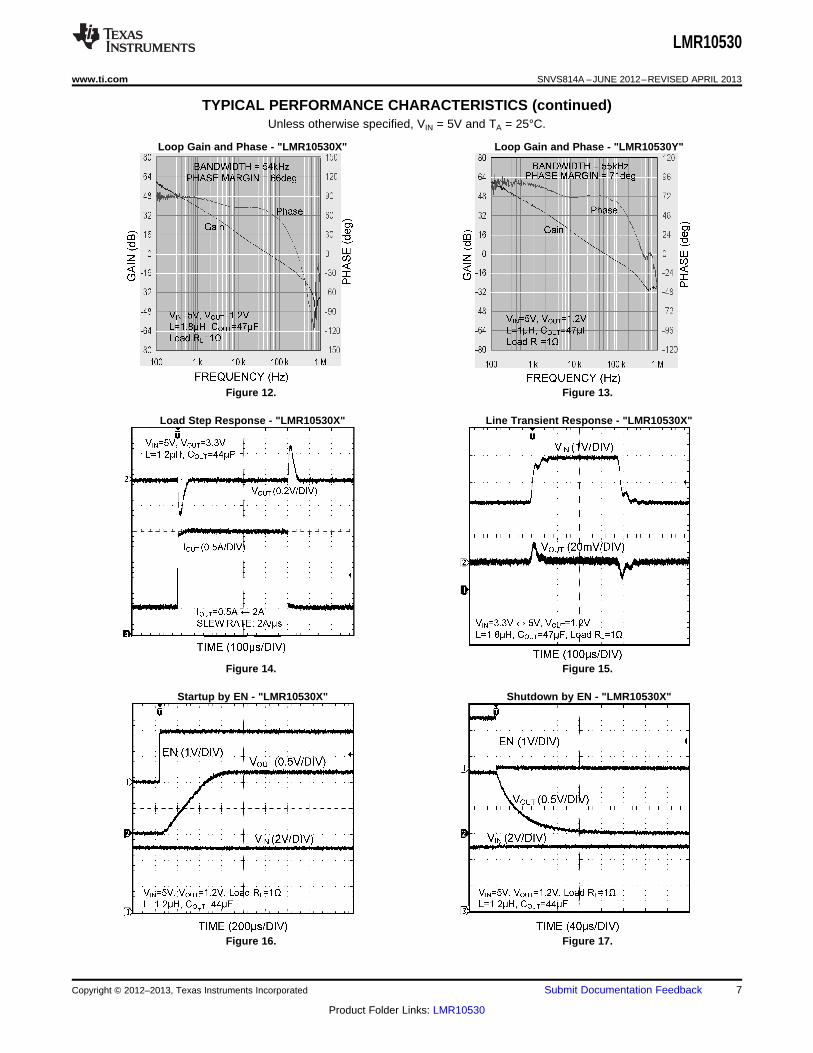
TYPICAL PERFORMANCE CHARACTERISTICS (continued)Unless otherwise specified, VIN = 5V and TA = 25°C.
Loop Gain and Phase - "LMR10530X" Loop Gain and Phase - "LMR10530Y"
Figure 12. Figure 13.
Load Step Response - "LMR10530X" Line Transient Response - "LMR10530X"
Figure 14. Figure 15.
Startup by EN - "LMR10530X" Shutdown by EN - "LMR10530X"
Figure 16. Figure 17.
Copyright © 2012–2013, Texas Instruments Incorporated Submit Documentation Feedback 7
Product Folder Links: LMR10530

LMR10530
SNVS814A –JUNE 2012–REVISED APRIL 2013 www.ti.com
TYPICAL PERFORMANCE CHARACTERISTICS (continued)Unless otherwise specified, VIN = 5V and TA = 25°C
Startup with EN tied to VIN - "LMR10530X" Short-circuit Triggering - "LMR10530X"
Figure 18. Figure 19.
Short-circuit Release - "LMR10530X" Recovery from Thermal Shutdown - "LMR10530X"
Figure 20. Figure 21.
8 Submit Documentation Feedback Copyright © 2012–2013, Texas Instruments Incorporated
Product Folder Links: LMR10530

LMR10530
www.ti.com SNVS814A –JUNE 2012–REVISED APRIL 2013
Block Diagram
Figure 22. Simplified Block Diagram
Copyright © 2012–2013, Texas Instruments Incorporated Submit Documentation Feedback 9
Product Folder Links: LMR10530

0
0
VIN
-VD
TON
t
t
InductorCurrent
D = TON/TSW
VSW
TOFF
TSWIL
SWVoltage
'iLIOUT
ILPK
LMR10530
SNVS814A –JUNE 2012–REVISED APRIL 2013 www.ti.com
APPLICATION INFORMATION
THEORY OF OPERATION
The LMR10530 is a constant frequency PWM buck regulator IC that delivers a 3.0A load current. The regulator isavailable in preset switching frequencies of 1.5MHz or 3.0MHz. This high frequency allows the LMR10530 tooperate with small surface mount capacitors and inductors, resulting in a DC/DC converter that requires aminimum amount of board space. The LMR10530 is internally compensated, therefore it is simple to use andrequires few external components. The LMR10530 uses peak current-mode control to regulate the outputvoltage. The following description of operation of the LMR10530 will refer to the Typical Application Circuit, to thewaveforms in Figure 23 and simplified block diagram in Figure 22. The LMR10530 supplies a regulated outputvoltage by switching the internal PMOS power switch at a constant frequency and variable duty cycle. Aswitching cycle begins at the falling edge of the reset pulse generated by the internal oscillator. When this pulsegoes low, the output control logic turns on the internal PMOS power switch. During this on-time, the SW pinvoltage (VSW) swings up to approximately VIN, and the inductor current (IL) increases with a linear slope. IL ismeasured by the current sense amplifier, which generates an output proportional to the switch current. Thesense signal is summed with the regulator’s corrective ramp and compared to the error amplifier’s output, whichis proportional to the difference between the feedback voltage and VREF. When the PWM comparator output goeshigh, the internal power switch turns off until the next switching cycle begins. During the switch off-time, theinductor current discharges through the catch diode D1, which forces the SW pin to swing below ground by theforward voltage (VD) of the catch diode. The regulator loop adjusts the duty cycle (D) to maintain a constantoutput voltage.
Figure 23. SW Pin Voltage and Inductor Current Waveforms
10 Submit Documentation Feedback Copyright © 2012–2013, Texas Instruments Incorporated
Product Folder Links: LMR10530

LMR10530
www.ti.com SNVS814A –JUNE 2012–REVISED APRIL 2013
SOFT-START/SHUTDOWN
The LMR10530 has both enable and shutdown modes that are controlled by the EN pin. Connecting a voltagesource greater than 1.8V to the EN pin enables the operation of the LMR10530, while reducing this voltagebelow 0.4V places the part in a low quiescent current (300nA typical) shutdown mode. There is no internal pull-up on EN pin, therefore an external signal is required to initiate switching. Do not allow this pin to float or rise to0.3V above VIN. It should be noted that when the EN pin voltage rises above 1.8V while the input voltage isgreater than UVLO, there is 15µs delay before switching starts. During this delay the LMR10530 will go through apower on reset state after which the internal soft-start process commences. During soft-start, the error amplifier’sreference voltage ramps from 0V to its nominal value of 0.6V in approximately 600µs. This forces the regulatoroutput to ramp up in a controlled fashion, which helps reduce inrush current seen at the input and minimizesoutput voltage overshoot.
The simplest way to enable the operation of the LMR10530 is to connect the EN pin to VIN which allows selfstart-up of the LMR10530 whenever the input voltage is applied. However, when an input voltage of slow risetime is used to power the application and if both the input voltage and the output voltage are not fully establishedbefore the soft-start time elapses, the control circuit will command maximum duty cycle operation of the internalpower switch to bring up the output voltage rapidly. When the feedback pin voltage exceeds 0.6V, the duty cyclewill have to reduce from the maximum value accordingly, to maintain regulation. The reduction of duty cycletakes a finite amount of time and can result in a transient in output voltage for a short duration, as shown inFigure 24. In applications where this output voltage overshoot is undesirable, one simple solution is to add afeed-forward capacitor CFF) across the top feedback resistor R1 to speed Gm Amplifier recovery. In practice, a27nF to 100nF ceramic capacitor is usually a good choice to remove the overshoot completely or limit theovershoot to an insignificant level during startup, as shown in Figure 25. Another more effective solution is tocontrol EN pin voltage by a separate logic signal, and pull the signal high only after VIN is fully established. In thisway, the chip can execute a normal, complete soft start process, minimizing any output voltage overshoot. Undersome circumstances at cold temperature, this approach may also be required to minimize any unwanted outputvoltage transients that may occur when the input voltage rises slowly. For a fast rising input voltage (100µs forexample), there is no need to control EN separately or add a feed-forward capacitor since the soft-start can bringup output voltage smoothly as shown in Figure 26.
During startup, the LMR10530 gradually increases the switching frequency from 400kHz (LMR10530X) or800kHz (LMR10530Y) to the nominal fixed value, as the feedback voltage increases (see Frequency Foldbacksection for more information). Since the internal corrective ramp signal adjusts its slope dynamically, and isproportional to the switching frequency during startup, a larger output capacitance may be required to insure asmooth output voltage rise, at low programmed output voltage and high output load current.
Figure 24. Startup Response to VIN
Copyright © 2012–2013, Texas Instruments Incorporated Submit Documentation Feedback 11
Product Folder Links: LMR10530

LMR10530
SNVS814A –JUNE 2012–REVISED APRIL 2013 www.ti.com
Figure 25. Startup Response to VIN with CFF
Figure 26. Startup Response to VIN with 100µs rise time
FREQUENCY FOLDBACK
The LMR10530 uses frequency foldback to help limit switch current and power dissipation during start-up, short-circuit and over load conditions by sensing if the feedback voltage is below 0.32V (typical). The LMR10530 willreduce the switching frequency from the nominal fixed value (1.5MHz or 3.0MHz) down to 400kHz (LMR10530X)or 800kHz (LMR10530Y) when the feedback voltage drops to 0V. See the Frequency Foldback plot in the TypicalPerformance Characteristics section.
12 Submit Documentation Feedback Copyright © 2012–2013, Texas Instruments Incorporated
Product Folder Links: LMR10530

LMR10530
www.ti.com SNVS814A –JUNE 2012–REVISED APRIL 2013
LOAD STEP RESPONSE
The LMR10530 has a fixed internal loop compensation, which results in a small-signal loop bandwidth highlyrelated to the output voltage level. In general, the loop bandwidth at low voltage is larger than at high voltage dueto the increased overall loop gain. The limited bandwidth at high output voltage may pose a challenge when loopstep response is concerned. In this case, one effective approach to improving loop step response is to add afeed-forward capacitor CFF) in the range of 27nF to 100nF in parallel with the upper feedback resistor (assumingthe lower feedback resistor is 2kΩ), as shown in Figure 27. The feed-forward capacitor introduces a zero-polepair which helps compensate the loop. The position of the zero-pole pair is a function of the feedback resistorsand capacitor:
(1)
(2)
Note the factor in parenthesis is the ratio of the output voltage to the feedback voltage. As the output voltagegets close to 0.6V, the pole moves towards the zero, tending to cancel it out. Consequently, adding CFF will haveless effect on the step response at lower output voltages.
As an example, Figure 29 shows that at the output voltage of 3.3V, a 47nF of CFF can boost the loop bandwidthto 117kHz, from the original 23kHz as shown in Figure 28. Correspondingly, the responses to a load stepbetween 0.3A and 3A without and with CFF are shown in Figure 30 and Figure 31 respectively. The higher loopbandwidth as a result of CFF reduces the total output excursion by more than half.
Aside from the above approach, increasing the output capacitance is generally also effective to reduce theexcursion in output voltage caused by a load step. This approach remains valid for applications where thedesired output voltages are close to the feedback voltage.
Figure 27. Adding a CFF Capacitor
Copyright © 2012–2013, Texas Instruments Incorporated Submit Documentation Feedback 13
Product Folder Links: LMR10530

LMR10530
SNVS814A –JUNE 2012–REVISED APRIL 2013 www.ti.com
Figure 28. Loop Gain and Phase without CFF
Figure 29. Loop Gain and Phase with CFF
14 Submit Documentation Feedback Copyright © 2012–2013, Texas Instruments Incorporated
Product Folder Links: LMR10530

LMR10530
www.ti.com SNVS814A –JUNE 2012–REVISED APRIL 2013
Figure 30. Load Step Response without CFF
Figure 31. Load Step Response with CFF
OUTPUT OVER-VOLTAGE PROTECTION
The LMR10530 has a built in output over-voltage comparator that compares the FB pin voltage to a thresholdvoltage that is 15% higher than the internal reference VREF. Once the FB pin voltage exceeds this threshold level(typically 0.69V), the internal PMOS power switch is turned off, which allows the output voltage to decreasetowards regulation.
UNDER-VOLTAGE LOCKOUT
Under-voltage lockout (UVLO) prevents the LMR10530 from operating until the input voltage exceeds 2.70V(typical). The UVLO threshold has approximately 350mV of hysteresis, so the part will operate until VIN dropsbelow 2.35V (typical). Hysteresis prevents the part from turning off during power up if VIN is non-monotonic.
Copyright © 2012–2013, Texas Instruments Incorporated Submit Documentation Feedback 15
Product Folder Links: LMR10530

r ='iLlOUT
D =VOUT + VD
VIN + VD - VSW
D =VOUT
VIN
LMR10530
SNVS814A –JUNE 2012–REVISED APRIL 2013 www.ti.com
CURRENT LIMIT
The LMR10530 uses cycle-by-cycle current limiting to protect the internal power switch. During each switchingcycle, a current limit comparator detects if the power switch current exceeds 4.4A (typical), and turns off theswitch until the next switching cycle begins.
THERMAL SHUTDOWN
Thermal shutdown limits total power dissipation by turning off the internal power switch when the IC junctiontemperature typically exceeds 165°C. After thermal shutdown occurs, the power switch does not turn on againuntil the junction temperature drops below approximately 150°C.
Design Guide
INDUCTOR SELECTION
The Duty Cycle (D) can be approximated quickly using the ratio of output voltage (VOUT) to input voltage (VIN):
(3)
The catch diode (D1) forward voltage drop and the voltage drop across the internal PMOS must be included tocalculate a more accurate duty cycle. Calculate D by using the following formula:
(4)
VSW can be approximated by:VSW = IOUT x RDS(ON)
where• IOUT is output load current. (5)
The diode forward drop (VD) can range from 0.3V to 0.7V depending on the quality of the diode. The lower theVD, the higher the operating efficiency of the converter.
The inductor value determines the output ripple current (ΔiL, as defined in Figure 23). Lower inductor valuesdecrease the size of the inductor, but increase the output ripple current. An increase in the inductor value willdecrease the output ripple current. In general, the ratio of ripple current to the output current is optimized when itis set between 0.2 and 0.4 for output currents above 2A. This ratio r is defined as:
(6)
One must ensure that the minimum current limit (3.4A) is not exceeded, so the peak current in the inductor mustbe calculated. The peak current (ILPK) in the inductor is calculated by:
ILPK = IOUT + ΔiL/2 (7)
When the designed maximum output current is reduced, the ratio r can be increased. At a current of 0.1A, r canbe made as high as 0.9. The ripple ratio can be increased at lighter loads because the net ripple is actually quitelow, and if r remains constant the inductor value can be made quite large. An equation empirically developed forthe maximum ripple ratio at any current below 2A is:
r = 0.387 x IOUT-0.3667 (8)
Note that this is just a guideline, and it needs to be combined with two important factors for proper selection ofinductance values at any operating condition. The first consideration is at output voltage above 2.5V, one needsto ensure that the inductance given by the above guideline should not be less than 1µH for the LMR10530X or0.5µH for the LMR10530Y. Since the LMR10530 has a fixed internal corrective ramp signal, a very lowinductance value at high output voltage will generate a very steep down slope of inductor current, which willresult in an insufficient slope compensation, and cause instability known as sub-harmonic oscillation. Anotherconsideration is at low load current, one needs to ensure that the inductance value given by the guideline shouldnot exceed 10µH for the LMR10530X and 4.7µH for the LMR10530Y, since too much inductance effectivelyflattens the down slope of the inductor current, and may significantly limit the system bandwidth and phasemargin resulting in instability.
16 Submit Documentation Feedback Copyright © 2012–2013, Texas Instruments Incorporated
Product Folder Links: LMR10530

'VOUT = 'IL RESR +8 x fSW x COUT
1
IRMS-IN = IOUT x D x 1 - D
IRMS-IN = IOUT x D x r2
121 - D +
L =VOUT + VD
IOUT x r x fSWx (1-D)
LMR10530
www.ti.com SNVS814A –JUNE 2012–REVISED APRIL 2013
The LMR10530 operates at frequencies allowing the use of ceramic output capacitors without compromisingtransient response. Ceramic capacitors allow higher inductor ripple without significantly increasing output ripple.See the Output Capacitor section for more details on calculating output voltage ripple.
Now that the ripple current is determined, the inductance is calculated by:
where• fSW is the switching frequency. (9)
When selecting an inductor, make sure that it is capable of supporting the peak output current without saturating.Inductor saturation will result in a sudden reduction in inductance and prevent the regulator from operatingproperly. Because of the operating frequency of the LMR10530, ferrite based inductors are preferred to minimizecore losses. This presents little restriction since the variety and availability of ferrite-based inductors is large.Lastly, inductors with lower series resistance (DCR) will provide better operating efficiency. For recommendedinductor selection, refer to Design Examples.
INPUT CAPACITOR
An input capacitor is necessary to ensure that VIN does not drop excessively during switching transients. Theprimary specifications of the input capacitor are capacitance, voltage rating, RMS current rating, and ESL(Equivalent Series Inductance). The input voltage rating is specifically stated by the capacitor manufacturer.Make sure to check any recommended deratings and also verify if there is any significant change in capacitanceat the operating input voltage and the operating temperature. The input capacitor maximum RMS input currentrating (IRMS-IN) must be greater than:
(10)
Neglecting inductor ripple simplifies the above equation to:
(11)
It can be shown from the above equation that maximum RMS capacitor current occurs when D = 0.5. Alwayscalculate the RMS at the point where the duty cycle D is closest to 0.5. The ESL of an input capacitor is usuallydetermined by the effective cross sectional area of the current path. As a rule of thumb, a large leaded capacitorwill have high ESL and a 1206 ceramic chip capacitor will have very low ESL. At the operating frequencies of theLMR10530, leaded capacitors may have an ESL so large that the resulting impedance (2πfL) will be higher thanthat required to provide stable operation. It is strongly recommended to use ceramic capacitors due to their lowESR and low ESL. A 22µF multilayer ceramic capacitor (MLCC) is a good choice for most applications. In caseswhere large capacitance is required, use surface mount capacitors such as Tantalum capacitors and place atleast a 4.7µF ceramic capacitor close to the VIN pin. For MLCCs it is recommended to use X7R or X5Rdielectrics. Consult capacitor manufacturer datasheet to see how rated capacitance varies over operatingconditions.
OUTPUT CAPACITOR
The output capacitor is selected based upon the desired output ripple and transient response. The initial currentof a load transient is provided mainly by the output capacitor. The output ripple of the converter is:
(12)
When using MLCCs, the ESR is typically so low that the capacitive ripple may dominate. When this occurs, theoutput ripple will be approximately sinusoidal and 90° phase shifted from the switching action. Given theavailability and quality of MLCCs and the expected output voltage of designs using the LMR10530, there is reallyno need to review any other capacitor technologies. Another benefit of ceramic capacitors is their ability tobypass high frequency noise. A certain amount of switching edge noise will couple through parasiticcapacitances in the inductor to the output. A ceramic capacitor will bypass this noise while a tantalum will not.Since the output capacitor is one of the two external components that control the stability of the regulator controlloop, most applications will require a minimum of 22µF output capacitance. In the case of low output voltage, a
Copyright © 2012–2013, Texas Instruments Incorporated Submit Documentation Feedback 17
Product Folder Links: LMR10530

D =VOUT + VD + VDCR
VIN + VD - VSW
D =VOUT + VD
VIN + VD - VSW
K =POUT
POUT + PLOSS
K =POUT
PIN
x R2R1 =VREF
VOUT- 1
LMR10530
SNVS814A –JUNE 2012–REVISED APRIL 2013 www.ti.com
larger output capacitance is required to ensure sufficient phase margin. Capacitance can often, but not always,be increased significantly with little detriment to the regulator stability. Like the input capacitor, recommendedmultilayer ceramic capacitors are X7R or X5R types. Again, verify actual capacitance at the desired operatingvoltage and temperature. Check the RMS current rating of the capacitor. The maximum RMS current rating of thecapacitor is:
(13)
One may select a 1206 size MLCC for output capacitor, since its current rating is typically above 1A, more thanenough for the requirement.
CATCH DIODE
The catch diode conducts during the switch off-time. A Schottky diode is recommended for its fast switching timeand low forward voltage drop. The catch diode should be chosen such that its current rating is greater than:
ID = IOUT x (1-D) (14)
The reverse breakdown rating of the diode must be at least the maximum input voltage plus appropriate margin.To improve efficiency, choose a Schottky diode with a low forward voltage drop.
OUTPUT VOLTAGE
The output voltage is set using the following equation where R2 is connected between the FB pin and GND, andR1 is connected between VOUT and the FB pin. A good value for R2 is 2kΩ.
(15)VREF = 0.60V (16)
EFFICIENCY ESTIMATION
The complete LMR10530 DC/DC converter efficiency can be calculated in the following manner:
(17)
Or
(18)
Calculations for determining the most significant power losses are shown below. Other losses totaling less than2% are not discussed.
The main power loss (PLOSS) in the converter includes two basic types of losses: switching loss and conductionloss. In addition, there is loss associated with the power required for the internal circuitry of IC. Conductionlosses usually dominate at higher output loads, whereas switching losses dominate at lower output loads. Thefirst step in determining the losses is to calculate the duty cycle (D):
(19)
VSW is the voltage drop across the internal power switch when it is on, and is equal to:VSW = IOUT x RDS(ON) (20)
VD is the forward voltage drop across the catch diode. It can be obtained from the diode manufactures ElectricalCharacteristics section. If the DC voltage drop across the inductor (VDCR) is accounted for, the equationbecomes:
(21)
The conduction losses in the catch diode are calculated as follows:PDIODE = VD x IOUT x (1-D) (22)
18 Submit Documentation Feedback Copyright © 2012–2013, Texas Instruments Incorporated
Product Folder Links: LMR10530

PCOND= (IOUT2 x D) x
13
1 + x'iLIOUT
2
x RDS (ON)
LMR10530
www.ti.com SNVS814A –JUNE 2012–REVISED APRIL 2013
Often this is the single most significant power loss in the circuit. Care should be taken to choose a Schottkydiode with a low forward voltage drop.
Another significant external power loss is the conduction loss in the output inductor. The equation can besimplified to:
PIND = IOUT2 x RDCR (23)
The LMR10530 conduction loss is mainly associated with the internal power switch:
(24)
If the inductor ripple current is fairly small, the conduction losses can be simplified to:PCOND = IOUT
2 x RDS(ON) x D (25)
Switching losses are also associated with the internal power switch. They occur during the switch on and offtransition periods, where voltages and currents overlap resulting in power loss. The simplest means to determinethis loss is to empirically measuring the rise and fall times (10% to 90%) of the switch at the switch node.
Switching Power Loss is calculated as follows:PSWR = 0.5 x (VIN x IOUT x fSW x TRISE) (26)PSWF = 0.5 x (VIN x IOUT x fSW x TFALL) (27)PSW = PSWR + PSWF (28)
The power loss required for operation of the internal circuitry is given by:PQ = IQ x VIN (29)
IQ is the quiescent operating current, and is typically around 3.2mA for the LMR10530X, and 4.3mA for theLMR10530Y.
An example of efficiency calculation for a typical application is shown in Table 1:
Table 1. Power Loss Tabulation
Conditions Power loss
VIN 5V
VOUT 3.3V
IOUT 3.0A POUT 9.9W
VD 0.33V PDIODE 277mW
RDS(ON) 56mΩ PCOND 363mW
fSW 1.5MHz
TRISE 10nsPSW 225mW
TFALL 10ns
INDDCR 28mΩ PIND 252mW
IQ 3.2mA PQ 16mW
η 89.7%
D is calculated to be 0.72
PLOSS = Σ ( PCOND + PSW + PQ + PIND + PDIODE ) (30)PLOSS = 1.133W (31)
Copyright © 2012–2013, Texas Instruments Incorporated Submit Documentation Feedback 19
Product Folder Links: LMR10530

LMR10530
SNVS814A –JUNE 2012–REVISED APRIL 2013 www.ti.com
PCB LAYOUT CONSIDERATIONS
When planning layout there are a few things to consider to achieve a clean, regulated output. The most importantconsideration is the close coupling of the GND connections of the input capacitor Cin and the catch diode D1.These ground ends should be close to one another and be connected to the GND plane with at least twothrough-holes. Place these components as close to the IC as possible. The next consideration is the location ofthe GND connection of the output capacitor Co, which should be near the GND connections of C1 and D1. Thereshould be a continuous ground plane on the bottom layer of a two-layer board except under the switching nodeisland. The signal ground SGND (pin 3) and power ground PGND (pin 6) should be tied together and connectedto ground plane through vias.
The FB pin is a high impedance node and care should be taken to make the FB trace short to avoid noise pickupthat causes inaccurate regulation. The feedback resistors should be placed as close as possible to the IC, withthe GND of Rfbb placed as close as possible to the SGND of the IC. The VOUT trace to Rfb1 should be routedaway from the inductor and any other traces that are switching.
High AC currents flow through the VIN, SW and VOUT traces, so they should be as short and wide as possible.Radiated noise can be decreased by choosing a shielded inductor.
The remaining components should also be placed as close as possible to the IC. Please see Application NoteAN-2280 SNVU192 for further considerations and the LMR10530 demo board as an example of a four-layerlayout.
20 Submit Documentation Feedback Copyright © 2012–2013, Texas Instruments Incorporated
Product Folder Links: LMR10530

LMR10530X
VIN VIND SW
FB
SGND
L1
R1
D1
C1
VOUT
VINC
PGND
C2
R2
EN
1
2
3 6
5
7,89,10
R3
C3 4NC
LMR10530
www.ti.com SNVS814A –JUNE 2012–REVISED APRIL 2013
LMR10530X Design Example 1
Figure 32. LMR10530X (1.5MHz): VIN = 3.3V, Output = 1.2V/3.0A
Table 2. Bill of Materials
Part ID Part Value Manufacturer Part Number
U1 3.0A Buck Regulator TI LMR10530X
C1, Input Cap 22µF, 6.3V, X5R TDK C3216X5R0J226M
C2, Output Cap 47µF, 6.3V, X5R TDK C3216X5R0J476M
C3, Bypass Cap 0.22µF, 10V, X7R Murata GRM216R71A224KC01D
D1, Catch Diode Schottky, 0.33V at 3A, VR=30V Toshiba CMS01
L1 1.8µH, 3.6A TDK LTF5022T-1R8N3R6
R1 2.0kΩ, 1% Vishay CRCW08052K00FKEA
R2 2.0kΩ, 1% Vishay CRCW08052K00FKEA
R3 10Ω, 1% Vishay CRCW080510R0FKEA
Copyright © 2012–2013, Texas Instruments Incorporated Submit Documentation Feedback 21
Product Folder Links: LMR10530

LMR10530
SNVS814A –JUNE 2012–REVISED APRIL 2013 www.ti.com
LMR10530X Design Example 2
Figure 33. LMR10530X (1.5MHz): VIN = 5V, Output = 3.3V/3.0A
Table 3. Bill of Materials
Part ID Part Value Manufacturer Part Number
U1 3.0A Buck Regulator TI LMR10530X
C1, Input Cap 22µF, 6.3V, X5R TDK C3216X5R0J226M
C2, Output Cap 47µF, 6.3V, X5R TDK C3216X5R0J476M
C3, Bypass Cap 0.22µF, 10V, X7R Murata GRM216R71A224KC01D
CFF, Feed-forward Cap 47nF, 10V, X7R AVX 0805ZC473JAZ2A
D1, Catch Diode Schottky, 0.43V at 3A, VR=30V Vishay SSA33L-E3/61T
L1 1.2µH, 4.2A TDK LTF5022T-1R2N4R2
R1 10.2kΩ, 1% Vishay CRCW080510K2FKEA
R2 2.26kΩ, 1% Vishay CRCW08052K26FKEA
R3 10Ω, 1% Vishay CRCW080510R0FKEA
22 Submit Documentation Feedback Copyright © 2012–2013, Texas Instruments Incorporated
Product Folder Links: LMR10530

LMR10530Y
VIN VIND
SW
FB
SGND
L1
R1
D1
C1
VOUT
VINC
PGND
C2
R2
EN
1
2
3 6
5
7,89,10
R3
C3 4NC
LMR10530
www.ti.com SNVS814A –JUNE 2012–REVISED APRIL 2013
LMR10530Y Design Example 3
Figure 34. LMR10530Y (3MHz): VIN = 3.3V, Output = 1.2V/3.0A
Table 4. Bill of Materials
Part ID Part Value Manufacturer Part Number
U1 3.0A Buck Regulator TI LMR10530Y
C1, Input Cap 22µF, 6.3V, X5R TDK C3216X5R0J226M
C2, Output Cap 47µF, 6.3V, X5R TDK C3216X5R0J476M
C3, Bypass Cap 0.22µF, 10V, X7R Murata GRM216R71A224KC01D
D1, Catch Diode Schottky, 0.33V at 3A, VR=30V Toshiba CMS01
L1 1.0µH, 4.0A Taiyo Yuden NP04SZB1R0N
R1 2.0kΩ, 1% Vishay CRCW08052K00FKEA
R2 2.0kΩ, 1% Vishay CRCW08052K00FKEA
R3 10Ω, 1% Vishay CRCW080510R0FKEA
Copyright © 2012–2013, Texas Instruments Incorporated Submit Documentation Feedback 23
Product Folder Links: LMR10530

LMR10530
SNVS814A –JUNE 2012–REVISED APRIL 2013 www.ti.com
LMR10530Y Design Example 4
Figure 35. LMR10530Y (3MHz): VIN = 5V, Output = 3.3V/3.0A
Table 5. Bill of Materials
Part ID Part Value Manufacturer Part Number
U1 3.0A Buck Regulator TI LMR10530Y
C1, Input Cap 22µF, 6.3V, X5R TDK C3216X5R0J226M
C2, Output Cap 47µF, 6.3V, X5R TDK C3216X5R0J476M
C3, Bypass Cap 0.22µF, 10V, X7R Murata GRM216R71A224KC01D
CFF, Feed-forward Cap 47nF, 10V, X7R AVX 0805ZC473JAZ2A
D1, Catch Diode Schottky, 0.43V at 3A, VR=30V Vishay SSA33L-E3/61T
L1 1.0µH, 4.0A Taiyo Yuden NP04SZB1R0N
R1 10.2kΩ, 1% Vishay CRCW080510K2FKEA
R2 2.26kΩ, 1% Vishay CRCW08052K26FKEA
R3 10Ω, 1% Vishay CRCW080510R0FKEA
24 Submit Documentation Feedback Copyright © 2012–2013, Texas Instruments Incorporated
Product Folder Links: LMR10530

LMR10530
www.ti.com SNVS814A –JUNE 2012–REVISED APRIL 2013
REVISION HISTORY
Changes from Original (April 2013) to Revision A Page
• Changed layout of National Data Sheet to TI format .......................................................................................................... 24
Copyright © 2012–2013, Texas Instruments Incorporated Submit Documentation Feedback 25
Product Folder Links: LMR10530

PACKAGE OPTION ADDENDUM
www.ti.com 13-Aug-2015
Addendum-Page 1
PACKAGING INFORMATION
Orderable Device Status(1)
Package Type PackageDrawing
Pins PackageQty
Eco Plan(2)
Lead/Ball Finish(6)
MSL Peak Temp(3)
Op Temp (°C) Device Marking(4/5)
Samples
LMR10530XSD/NOPB ACTIVE WSON DSC 10 1000 Green (RoHS& no Sb/Br)
CU SN Level-1-260C-UNLIM -40 to 125 L287B
LMR10530XSDX/NOPB ACTIVE WSON DSC 10 4500 Green (RoHS& no Sb/Br)
CU SN Level-1-260C-UNLIM -40 to 125 L287B
LMR10530YSD/NOPB ACTIVE WSON DSC 10 1000 Green (RoHS& no Sb/Br)
CU SN Level-1-260C-UNLIM -40 to 125 L286B
LMR10530YSDX/NOPB ACTIVE WSON DSC 10 4500 Green (RoHS& no Sb/Br)
CU SN Level-1-260C-UNLIM -40 to 125 L286B
(1) The marketing status values are defined as follows:ACTIVE: Product device recommended for new designs.LIFEBUY: TI has announced that the device will be discontinued, and a lifetime-buy period is in effect.NRND: Not recommended for new designs. Device is in production to support existing customers, but TI does not recommend using this part in a new design.PREVIEW: Device has been announced but is not in production. Samples may or may not be available.OBSOLETE: TI has discontinued the production of the device.
(2) Eco Plan - The planned eco-friendly classification: Pb-Free (RoHS), Pb-Free (RoHS Exempt), or Green (RoHS & no Sb/Br) - please check http://www.ti.com/productcontent for the latest availabilityinformation and additional product content details.TBD: The Pb-Free/Green conversion plan has not been defined.Pb-Free (RoHS): TI's terms "Lead-Free" or "Pb-Free" mean semiconductor products that are compatible with the current RoHS requirements for all 6 substances, including the requirement thatlead not exceed 0.1% by weight in homogeneous materials. Where designed to be soldered at high temperatures, TI Pb-Free products are suitable for use in specified lead-free processes.Pb-Free (RoHS Exempt): This component has a RoHS exemption for either 1) lead-based flip-chip solder bumps used between the die and package, or 2) lead-based die adhesive used betweenthe die and leadframe. The component is otherwise considered Pb-Free (RoHS compatible) as defined above.Green (RoHS & no Sb/Br): TI defines "Green" to mean Pb-Free (RoHS compatible), and free of Bromine (Br) and Antimony (Sb) based flame retardants (Br or Sb do not exceed 0.1% by weightin homogeneous material)
(3) MSL, Peak Temp. - The Moisture Sensitivity Level rating according to the JEDEC industry standard classifications, and peak solder temperature.
(4) There may be additional marking, which relates to the logo, the lot trace code information, or the environmental category on the device.
(5) Multiple Device Markings will be inside parentheses. Only one Device Marking contained in parentheses and separated by a "~" will appear on a device. If a line is indented then it is a continuationof the previous line and the two combined represent the entire Device Marking for that device.
(6) Lead/Ball Finish - Orderable Devices may have multiple material finish options. Finish options are separated by a vertical ruled line. Lead/Ball Finish values may wrap to two lines if the finishvalue exceeds the maximum column width.

PACKAGE OPTION ADDENDUM
www.ti.com 13-Aug-2015
Addendum-Page 2
Important Information and Disclaimer:The information provided on this page represents TI's knowledge and belief as of the date that it is provided. TI bases its knowledge and belief on informationprovided by third parties, and makes no representation or warranty as to the accuracy of such information. Efforts are underway to better integrate information from third parties. TI has taken andcontinues to take reasonable steps to provide representative and accurate information but may not have conducted destructive testing or chemical analysis on incoming materials and chemicals.TI and TI suppliers consider certain information to be proprietary, and thus CAS numbers and other limited information may not be available for release.
In no event shall TI's liability arising out of such information exceed the total purchase price of the TI part(s) at issue in this document sold by TI to Customer on an annual basis.

TAPE AND REEL INFORMATION
*All dimensions are nominal
Device PackageType
PackageDrawing
Pins SPQ ReelDiameter
(mm)
ReelWidth
W1 (mm)
A0(mm)
B0(mm)
K0(mm)
P1(mm)
W(mm)
Pin1Quadrant
LMR10530XSD/NOPB WSON DSC 10 1000 178.0 12.4 3.3 3.3 1.0 8.0 12.0 Q1
LMR10530XSDX/NOPB WSON DSC 10 4500 330.0 12.4 3.3 3.3 1.0 8.0 12.0 Q1
LMR10530YSD/NOPB WSON DSC 10 1000 178.0 12.4 3.3 3.3 1.0 8.0 12.0 Q1
LMR10530YSDX/NOPB WSON DSC 10 4500 330.0 12.4 3.3 3.3 1.0 8.0 12.0 Q1
PACKAGE MATERIALS INFORMATION
www.ti.com 8-Apr-2013
Pack Materials-Page 1

*All dimensions are nominal
Device Package Type Package Drawing Pins SPQ Length (mm) Width (mm) Height (mm)
LMR10530XSD/NOPB WSON DSC 10 1000 210.0 185.0 35.0
LMR10530XSDX/NOPB WSON DSC 10 4500 367.0 367.0 35.0
LMR10530YSD/NOPB WSON DSC 10 1000 210.0 185.0 35.0
LMR10530YSDX/NOPB WSON DSC 10 4500 367.0 367.0 35.0
PACKAGE MATERIALS INFORMATION
www.ti.com 8-Apr-2013
Pack Materials-Page 2

MECHANICAL DATA
DSC0010A
www.ti.com
SDA10A (Rev A)

IMPORTANT NOTICE
Texas Instruments Incorporated (TI) reserves the right to make corrections, enhancements, improvements and other changes to itssemiconductor products and services per JESD46, latest issue, and to discontinue any product or service per JESD48, latest issue. Buyersshould obtain the latest relevant information before placing orders and should verify that such information is current and complete.TI’s published terms of sale for semiconductor products (http://www.ti.com/sc/docs/stdterms.htm) apply to the sale of packaged integratedcircuit products that TI has qualified and released to market. Additional terms may apply to the use or sale of other types of TI products andservices.Reproduction of significant portions of TI information in TI data sheets is permissible only if reproduction is without alteration and isaccompanied by all associated warranties, conditions, limitations, and notices. TI is not responsible or liable for such reproduceddocumentation. Information of third parties may be subject to additional restrictions. Resale of TI products or services with statementsdifferent from or beyond the parameters stated by TI for that product or service voids all express and any implied warranties for theassociated TI product or service and is an unfair and deceptive business practice. TI is not responsible or liable for any such statements.Buyers and others who are developing systems that incorporate TI products (collectively, “Designers”) understand and agree that Designersremain responsible for using their independent analysis, evaluation and judgment in designing their applications and that Designers havefull and exclusive responsibility to assure the safety of Designers' applications and compliance of their applications (and of all TI productsused in or for Designers’ applications) with all applicable regulations, laws and other applicable requirements. Designer represents that, withrespect to their applications, Designer has all the necessary expertise to create and implement safeguards that (1) anticipate dangerousconsequences of failures, (2) monitor failures and their consequences, and (3) lessen the likelihood of failures that might cause harm andtake appropriate actions. Designer agrees that prior to using or distributing any applications that include TI products, Designer willthoroughly test such applications and the functionality of such TI products as used in such applications.TI’s provision of technical, application or other design advice, quality characterization, reliability data or other services or information,including, but not limited to, reference designs and materials relating to evaluation modules, (collectively, “TI Resources”) are intended toassist designers who are developing applications that incorporate TI products; by downloading, accessing or using TI Resources in anyway, Designer (individually or, if Designer is acting on behalf of a company, Designer’s company) agrees to use any particular TI Resourcesolely for this purpose and subject to the terms of this Notice.TI’s provision of TI Resources does not expand or otherwise alter TI’s applicable published warranties or warranty disclaimers for TIproducts, and no additional obligations or liabilities arise from TI providing such TI Resources. TI reserves the right to make corrections,enhancements, improvements and other changes to its TI Resources. TI has not conducted any testing other than that specificallydescribed in the published documentation for a particular TI Resource.Designer is authorized to use, copy and modify any individual TI Resource only in connection with the development of applications thatinclude the TI product(s) identified in such TI Resource. NO OTHER LICENSE, EXPRESS OR IMPLIED, BY ESTOPPEL OR OTHERWISETO ANY OTHER TI INTELLECTUAL PROPERTY RIGHT, AND NO LICENSE TO ANY TECHNOLOGY OR INTELLECTUAL PROPERTYRIGHT OF TI OR ANY THIRD PARTY IS GRANTED HEREIN, including but not limited to any patent right, copyright, mask work right, orother intellectual property right relating to any combination, machine, or process in which TI products or services are used. Informationregarding or referencing third-party products or services does not constitute a license to use such products or services, or a warranty orendorsement thereof. Use of TI Resources may require a license from a third party under the patents or other intellectual property of thethird party, or a license from TI under the patents or other intellectual property of TI.TI RESOURCES ARE PROVIDED “AS IS” AND WITH ALL FAULTS. TI DISCLAIMS ALL OTHER WARRANTIES ORREPRESENTATIONS, EXPRESS OR IMPLIED, REGARDING RESOURCES OR USE THEREOF, INCLUDING BUT NOT LIMITED TOACCURACY OR COMPLETENESS, TITLE, ANY EPIDEMIC FAILURE WARRANTY AND ANY IMPLIED WARRANTIES OFMERCHANTABILITY, FITNESS FOR A PARTICULAR PURPOSE, AND NON-INFRINGEMENT OF ANY THIRD PARTY INTELLECTUALPROPERTY RIGHTS. TI SHALL NOT BE LIABLE FOR AND SHALL NOT DEFEND OR INDEMNIFY DESIGNER AGAINST ANY CLAIM,INCLUDING BUT NOT LIMITED TO ANY INFRINGEMENT CLAIM THAT RELATES TO OR IS BASED ON ANY COMBINATION OFPRODUCTS EVEN IF DESCRIBED IN TI RESOURCES OR OTHERWISE. IN NO EVENT SHALL TI BE LIABLE FOR ANY ACTUAL,DIRECT, SPECIAL, COLLATERAL, INDIRECT, PUNITIVE, INCIDENTAL, CONSEQUENTIAL OR EXEMPLARY DAMAGES INCONNECTION WITH OR ARISING OUT OF TI RESOURCES OR USE THEREOF, AND REGARDLESS OF WHETHER TI HAS BEENADVISED OF THE POSSIBILITY OF SUCH DAMAGES.Unless TI has explicitly designated an individual product as meeting the requirements of a particular industry standard (e.g., ISO/TS 16949and ISO 26262), TI is not responsible for any failure to meet such industry standard requirements.Where TI specifically promotes products as facilitating functional safety or as compliant with industry functional safety standards, suchproducts are intended to help enable customers to design and create their own applications that meet applicable functional safety standardsand requirements. Using products in an application does not by itself establish any safety features in the application. Designers mustensure compliance with safety-related requirements and standards applicable to their applications. Designer may not use any TI products inlife-critical medical equipment unless authorized officers of the parties have executed a special contract specifically governing such use.Life-critical medical equipment is medical equipment where failure of such equipment would cause serious bodily injury or death (e.g., lifesupport, pacemakers, defibrillators, heart pumps, neurostimulators, and implantables). Such equipment includes, without limitation, allmedical devices identified by the U.S. Food and Drug Administration as Class III devices and equivalent classifications outside the U.S.TI may expressly designate certain products as completing a particular qualification (e.g., Q100, Military Grade, or Enhanced Product).Designers agree that it has the necessary expertise to select the product with the appropriate qualification designation for their applicationsand that proper product selection is at Designers’ own risk. Designers are solely responsible for compliance with all legal and regulatoryrequirements in connection with such selection.Designer will fully indemnify TI and its representatives against any damages, costs, losses, and/or liabilities arising out of Designer’s non-compliance with the terms and provisions of this Notice.
Mailing Address: Texas Instruments, Post Office Box 655303, Dallas, Texas 75265Copyright © 2017, Texas Instruments Incorporated