lm614 quad operational amplifier and adjustable reference ... · please be aware that an important...
TRANSCRIPT
LM614
www.ti.com SNOSC21B –MAY 2004–REVISED MAY 2004
LM614 Quad Operational Amplifier and Adjustable ReferenceCheck for Samples: LM614
1FEATURES • Wide operating current range: 17μA to 20mA• Tolerant of load capacitance
23• Op Amp• Low operating current: 450μA
APPLICATIONS• Wide supply voltage range: 4V to 36V
• Transducer bridge driver and signal• Wide common-mode range: V − to (V+− 1.8V)processing
• Wide differential input voltage: ±36V• Process and mass flow control systems
• Reference• Power supply voltage monitor
• Adjustable output voltage: 1.2V to 5.0V• Buffered voltage references for A/D's
• Initial tolerance: ±2.0%
DESCRIPTIONThe LM614 consists of four op-amps and a programmable voltage reference in a 16-pin package. The op-ampout-performs most single-supply op-amps by providing higher speed and bandwidth along with low supplycurrent. This device was specifically designed to lower cost and board space requirements in transducer, test,measurement and data acquisition systems.
Combining a stable voltage reference with four wide output swing op-amps makes the LM614 ideal for singlesupply transducers, signal conditioning and bridge driving where large common-mode-signals are common. Thevoltage reference consists of a reliable band-gap design that maintains low dynamic output impedance (1Ωtypical), initial tolerance (2.0%), and the ability to be programmed from 1.2V to 5.0V via two external resistors.The voltage reference is very stable even when driving large capacitive loads, as are commonly encountered inCMOS data acquisition systems.
As a member of National's new Super-Block™ family, the LM614 is a space-saving monolithic alternative to amultichip solution, offering a high level of integration without sacrificing performance.
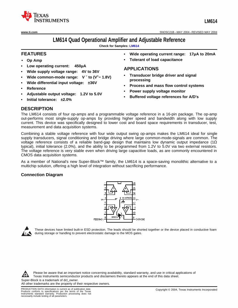
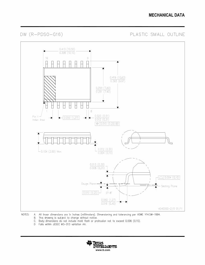
Connection Diagram
These devices have limited built-in ESD protection. The leads should be shorted together or the device placed in conductive foamduring storage or handling to prevent electrostatic damage to the MOS gates.
1
Please be aware that an important notice concerning availability, standard warranty, and use in critical applications ofTexas Instruments semiconductor products and disclaimers thereto appears at the end of this data sheet.
2Super-Block is a trademark of dcl_owner.3All other trademarks are the property of their respective owners.
PRODUCTION DATA information is current as of publication date. Copyright © 2004, Texas Instruments IncorporatedProducts conform to specifications per the terms of the TexasInstruments standard warranty. Production processing does notnecessarily include testing of all parameters.

LM614
SNOSC21B –MAY 2004–REVISED MAY 2004 www.ti.com
Absolute Maximum Ratings (1)
Voltage on Any Pins except VR
(referred to V− pin)(2) 36V (Max)(3) −0.3V (Min)
Current through Any Input Pin &
VR Pin ±20 mA
Differential Input Voltage
LM614I ±36V
LM614C ±32V
Storage Temperature Range −65°C ≤ TJ ≤ +150°C
Maximum Junction Temperature 150°C
Thermal Resistance, Junction-to-Ambient (4) 150°C
Soldering Information (Soldering, 10 sec.) 220°C
ESD Tolerance (5) ±1kV
(1) Absolute maximum ratings indicate limits beyond which damage to the component may occur. Electrical specifications do not applywhen operating the device beyond its rated operating conditions.
(2) Input voltage above V+ is allowed.(3) More accurately, it is excessive current flow, with resulting excess heating, that limits the voltages on all pins. When any pin is pulled a
diode drop below V−, a parasitic NPN transistor turns ON. No latch-up will occur as long as the current through that pin remains belowthe Maximum Rating. Operation is undefined and unpredictable when any parasitic diode or transistor is conducting.
(4) Junction temperature may be calculated using TJ = TA + P DθjA. The given thermal resistance is worst-case for packages in sockets instill air. For packages soldered to copper-clad board with dissipation from one comparator or reference output transistor, nominal θjA is90°C/W for the WM package.
(5) Human body model, 100 pF discharged through a 1.5 kΩ resistor.
Operating Temperature RangeLM614I −40°C ≤ TJ ≤ +85°C
LM614C 0°C ≤ TJ ≤ +70°C
2 Submit Documentation Feedback Copyright © 2004, Texas Instruments Incorporated
Product Folder Links: LM614
LM614
www.ti.com SNOSC21B –MAY 2004–REVISED MAY 2004
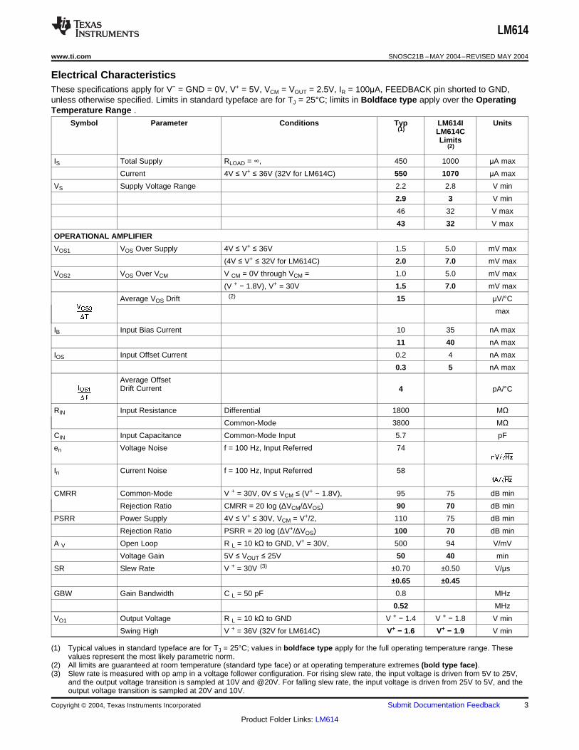
Electrical CharacteristicsThese specifications apply for V− = GND = 0V, V+ = 5V, VCM = VOUT = 2.5V, IR = 100μA, FEEDBACK pin shorted to GND,unless otherwise specified. Limits in standard typeface are for TJ = 25°C; limits in Boldface type apply over the OperatingTemperature Range .
Symbol Parameter Conditions Typ LM614I Units(1) LM614C
Limits(2)
IS Total Supply RLOAD = ∞, 450 1000 μA max
Current 4V ≤ V+ ≤ 36V (32V for LM614C) 550 1070 μA max
VS Supply Voltage Range 2.2 2.8 V min
2.9 3 V min
46 32 V max
43 32 V max
OPERATIONAL AMPLIFIER
VOS1 VOS Over Supply 4V ≤ V+ ≤ 36V 1.5 5.0 mV max
(4V ≤ V+ ≤ 32V for LM614C) 2.0 7.0 mV max
VOS2 VOS Over VCM V CM = 0V through VCM = 1.0 5.0 mV max
(V + − 1.8V), V+ = 30V 1.5 7.0 mV max
Average VOS Drift (2) 15 μV/°C
max
IB Input Bias Current 10 35 nA max
11 40 nA max
IOS Input Offset Current 0.2 4 nA max
0.3 5 nA max
Average OffsetDrift Current 4 pA/°C
RIN Input Resistance Differential 1800 MΩCommon-Mode 3800 MΩ
CIN Input Capacitance Common-Mode Input 5.7 pF
en Voltage Noise f = 100 Hz, Input Referred 74
In Current Noise f = 100 Hz, Input Referred 58
CMRR Common-Mode V + = 30V, 0V ≤ VCM ≤ (V+ − 1.8V), 95 75 dB min
Rejection Ratio CMRR = 20 log (ΔVCM/ΔVOS) 90 70 dB min
PSRR Power Supply 4V ≤ V+ ≤ 30V, VCM = V+/2, 110 75 dB min
Rejection Ratio PSRR = 20 log (ΔV+/ΔVOS) 100 70 dB min
A V Open Loop R L = 10 kΩ to GND, V+ = 30V, 500 94 V/mV
Voltage Gain 5V ≤ VOUT ≤ 25V 50 40 min
SR Slew Rate V + = 30V (3) ±0.70 ±0.50 V/μs
±0.65 ±0.45
GBW Gain Bandwidth C L = 50 pF 0.8 MHz
0.52 MHz
VO1 Output Voltage R L = 10 kΩ to GND V + − 1.4 V + − 1.8 V min
Swing High V + = 36V (32V for LM614C) V+ − 1.6 V+ − 1.9 V min
(1) Typical values in standard typeface are for TJ = 25°C; values in boldface type apply for the full operating temperature range. Thesevalues represent the most likely parametric norm.
(2) All limits are guaranteed at room temperature (standard type face) or at operating temperature extremes (bold type face).(3) Slew rate is measured with op amp in a voltage follower configuration. For rising slew rate, the input voltage is driven from 5V to 25V,
and the output voltage transition is sampled at 10V and @20V. For falling slew rate, the input voltage is driven from 25V to 5V, and theoutput voltage transition is sampled at 20V and 10V.
Copyright © 2004, Texas Instruments Incorporated Submit Documentation Feedback 3
Product Folder Links: LM614

LM614
SNOSC21B –MAY 2004–REVISED MAY 2004 www.ti.com
Electrical Characteristics (continued)These specifications apply for V− = GND = 0V, V+ = 5V, VCM = VOUT = 2.5V, IR = 100μA, FEEDBACK pin shorted to GND,unless otherwise specified. Limits in standard typeface are for TJ = 25°C; limits in Boldface type apply over the OperatingTemperature Range .
Symbol Parameter Conditions Typ LM614I Units(1) LM614C
Limits(2)
VO2 Output Voltage R L = 10 kΩ to V+ V − + 0.8 V − + 0.95 V max
Swing Low V + = 36V (32V for LM614C) V− + 0.9 V− + 1.0 V max
IOUT Output Source V OUT = 2.5V, V+IN = 0V, 25 16 mA min
V −IN = −0.3V 15 13 mA min
I SINK Output Sink V OUT = 1.6V, V+IN = 0V, 17 13 mA min
Current V −IN = 0.3V 9 8 mA min
ISHORT Short Circuit Current V OUT = 0V, V+IN = 3V, 30 50 mA max
V −IN = 2V, Source 40 60 mA max
V OUT = 5V, V+IN = 2V, 30 70 mA max
V −IN = 3V, Sink 32 90 mA max
VOLTAGE REFERENCE
VR Voltage Reference (4) 1.244 1.2191 V min
1.2689 V max
(±2.0%)
Average Temperature (5) 10 150 PPM/°C
Drift max
Hysteresis (6)
3.2 μV/°C
V R Change V R(100 μA) − VR(17 μA) 0.05 1 mV max
with Current 0.1 1.1 mV max
VR(10 mA) − VR(100 μA) 1.5 5 mV max(7) 2.0 5.5 mV max
R Resistance ΔV R(10→0.1 mA)/9.9 mA 0.2 0.56 Ω max
ΔV R(100→17 μA)/83 μA 0.6 13 Ω max
V R Change V R(Vro = Vr) − VR(Vro = 5.0V) 2.5 7 mV max
with High VRO (3.76V between Anode and 2.8 10 mV max
FEEDBACK)
V R Change with V R(V + = 5V) − VR(V + = 36V) 0.1 1.2 mV max
V+ Change (V+ = 32V for LM614C) 0.1 1.3 mV max
VR(V + = 5V) − VR(V + = 3V) 0.01 1 mV max
0.01 1.5 mV max
IFB FEEDBACK Bias V ANODE ≤ VFB ≤ 5.06V 22 50 nA max
Current 29 55 nA max
en Voltage Noise BW = 10 Hz to 10 kHz, 30 μV RMS
VRO = VR
(4) VR is the Cathode-feedback voltage, nominally 1.244V.(5) Average reference drift is calculated from the measurement of the reference voltage at 25°C and at the temperature extremes. The drift,
in ppm/°C, is 106•ΔV R/(VR[25°C] •ΔTJ), where ΔV R is the lowest value subtracted from the highest, VR[25°C] is the value at 25°C, and ΔTJis the temperature range. This parameter is guaranteed by design and sample testing.
(6) Hysteresis is the change in VR caused by a change in TJ, after the reference has been “dehysterized”. To dehysterize the reference; thatis minimize the hysteresis to the typical value, cycle its junction temperature in the following pattern, spiraling in toward 25°C: 25°C,85°C, −40°C, 70°C, 0°C, 25°C.
(7) Low contact resistance is required for accurate measurement.
4 Submit Documentation Feedback Copyright © 2004, Texas Instruments Incorporated
Product Folder Links: LM614
LM614
www.ti.com SNOSC21B –MAY 2004–REVISED MAY 2004
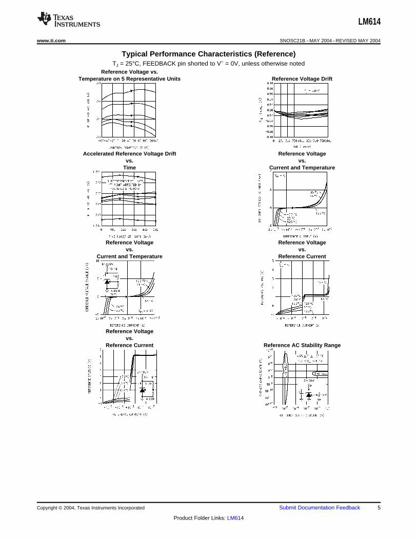
Typical Performance Characteristics (Reference)TJ = 25°C, FEEDBACK pin shorted to V− = 0V, unless otherwise noted
Reference Voltage vs.Temperature on 5 Representative Units Reference Voltage Drift
Accelerated Reference Voltage Drift Reference Voltagevs. vs.
Time Current and Temperature
Reference Voltage Reference Voltagevs. vs.
Current and Temperature Reference Current
Reference Voltagevs.
Reference Current Reference AC Stability Range
Copyright © 2004, Texas Instruments Incorporated Submit Documentation Feedback 5
Product Folder Links: LM614
LM614
SNOSC21B –MAY 2004–REVISED MAY 2004 www.ti.com
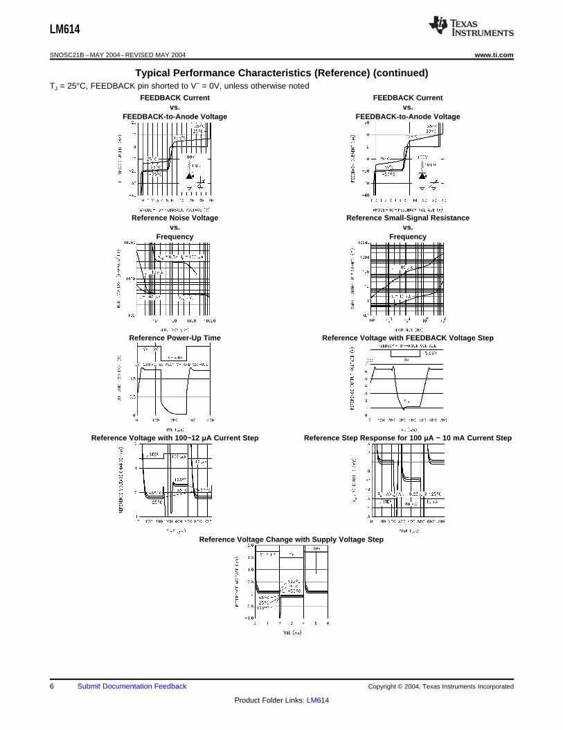
Typical Performance Characteristics (Reference) (continued)TJ = 25°C, FEEDBACK pin shorted to V− = 0V, unless otherwise noted
FEEDBACK Current FEEDBACK Currentvs. vs.
FEEDBACK-to-Anode Voltage FEEDBACK-to-Anode Voltage
Reference Noise Voltage Reference Small-Signal Resistancevs. vs.
Frequency Frequency
Reference Power-Up Time Reference Voltage with FEEDBACK Voltage Step
Reference Voltage with 100∼∼12 μA Current Step Reference Step Response for 100 μA ∼∼ 10 mA Current Step
Reference Voltage Change with Supply Voltage Step
6 Submit Documentation Feedback Copyright © 2004, Texas Instruments Incorporated
Product Folder Links: LM614
LM614
www.ti.com SNOSC21B –MAY 2004–REVISED MAY 2004
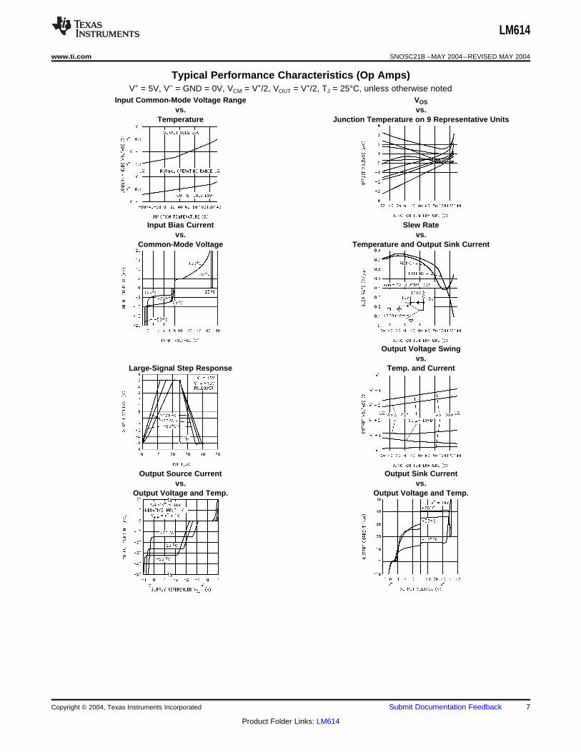
Typical Performance Characteristics (Op Amps)V+ = 5V, V− = GND = 0V, VCM = V+/2, VOUT = V+/2, TJ = 25°C, unless otherwise noted
Input Common-Mode Voltage Range VOSvs. vs.
Temperature Junction Temperature on 9 Representative Units
Input Bias Current Slew Ratevs. vs.
Common-Mode Voltage Temperature and Output Sink Current
Output Voltage Swingvs.
Large-Signal Step Response Temp. and Current
Output Source Current Output Sink Currentvs. vs.
Output Voltage and Temp. Output Voltage and Temp.
Copyright © 2004, Texas Instruments Incorporated Submit Documentation Feedback 7
Product Folder Links: LM614

LM614
SNOSC21B –MAY 2004–REVISED MAY 2004 www.ti.com
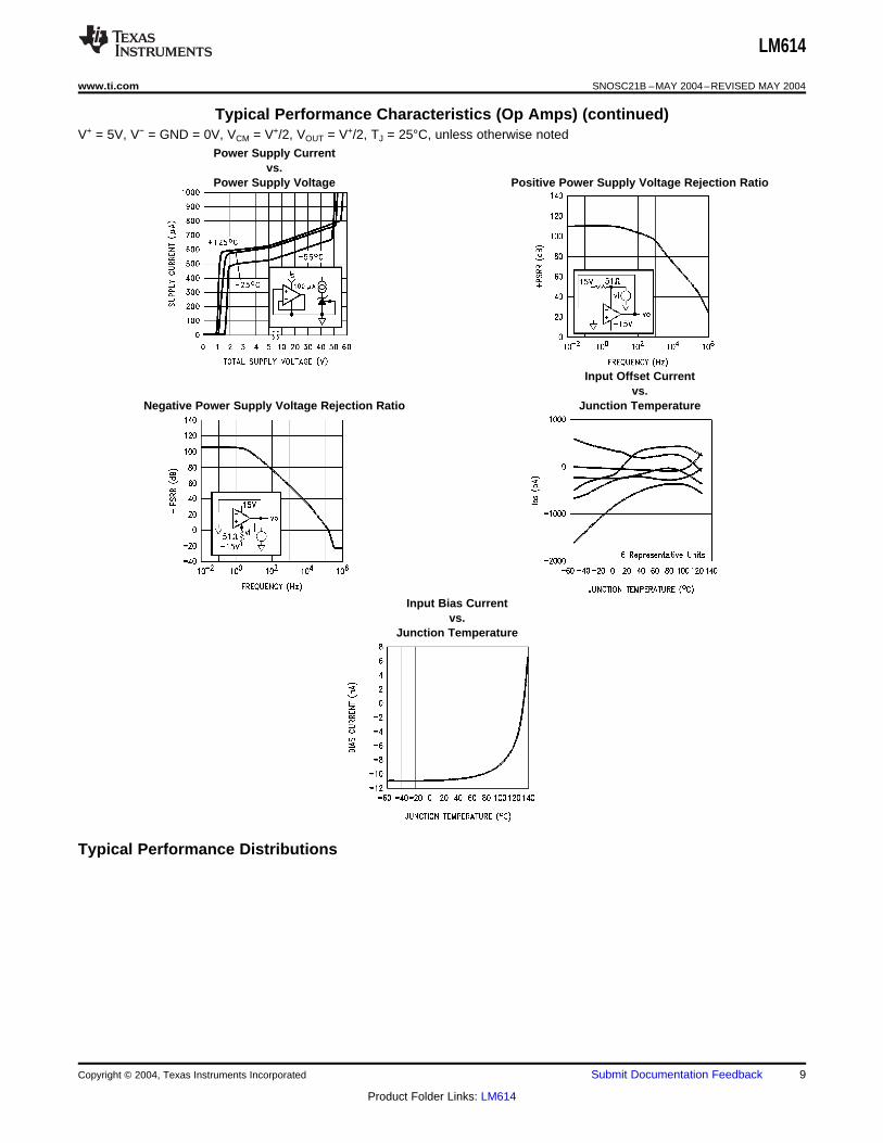
Typical Performance Characteristics (Op Amps) (continued)V+ = 5V, V− = GND = 0V, VCM = V+/2, VOUT = V+/2, TJ = 25°C, unless otherwise noted
Output Impedancevs.
Output Swing, Large Signal Frequency and Gain
Small-Signal Pulse Response Small-Signal Pulse Responsevs. vs.
Temp. Load
Op Amp Voltage Noise Op Amp Current Noisevs. vs.
Frequency Frequency
Small-Signal Voltage Gain Small-Signal Voltage Gainvs. vs.
Frequency and Temperature Frequency and Load
Follower Small-Signal Frequency Response Common-Mode Input Voltage Rejection Ratio
8 Submit Documentation Feedback Copyright © 2004, Texas Instruments Incorporated
Product Folder Links: LM614
LM614
www.ti.com SNOSC21B –MAY 2004–REVISED MAY 2004
Typical Performance Characteristics (Op Amps) (continued)V+ = 5V, V− = GND = 0V, VCM = V+/2, VOUT = V+/2, TJ = 25°C, unless otherwise noted
Power Supply Currentvs.
Power Supply Voltage Positive Power Supply Voltage Rejection Ratio
Input Offset Currentvs.
Negative Power Supply Voltage Rejection Ratio Junction Temperature
Input Bias Currentvs.
Junction Temperature
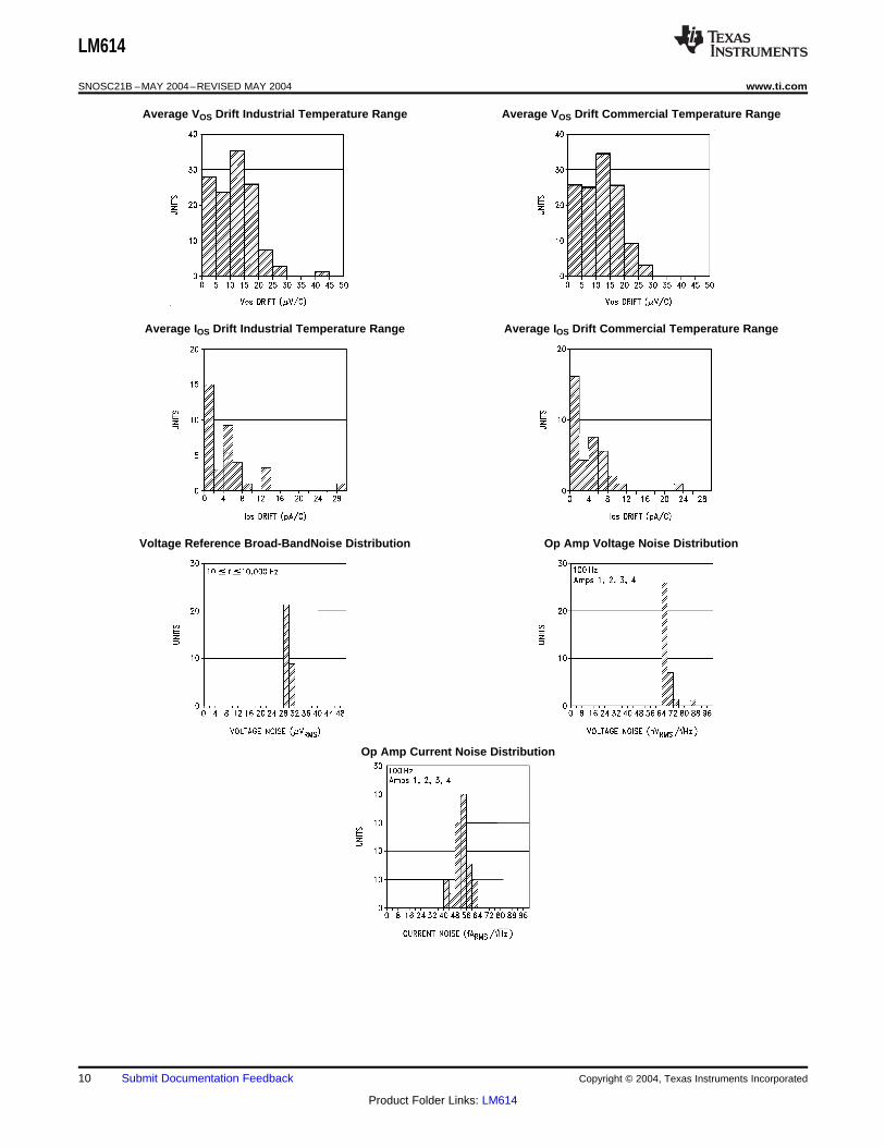
Typical Performance Distributions
Copyright © 2004, Texas Instruments Incorporated Submit Documentation Feedback 9
Product Folder Links: LM614
LM614
SNOSC21B –MAY 2004–REVISED MAY 2004 www.ti.com
Average VOS Drift Industrial Temperature Range Average VOS Drift Commercial Temperature Range
Average IOS Drift Industrial Temperature Range Average IOS Drift Commercial Temperature Range
Voltage Reference Broad-BandNoise Distribution Op Amp Voltage Noise Distribution
Op Amp Current Noise Distribution
10 Submit Documentation Feedback Copyright © 2004, Texas Instruments Incorporated
Product Folder Links: LM614
LM614
www.ti.com SNOSC21B –MAY 2004–REVISED MAY 2004
Application Information
VOLTAGE REFERENCE
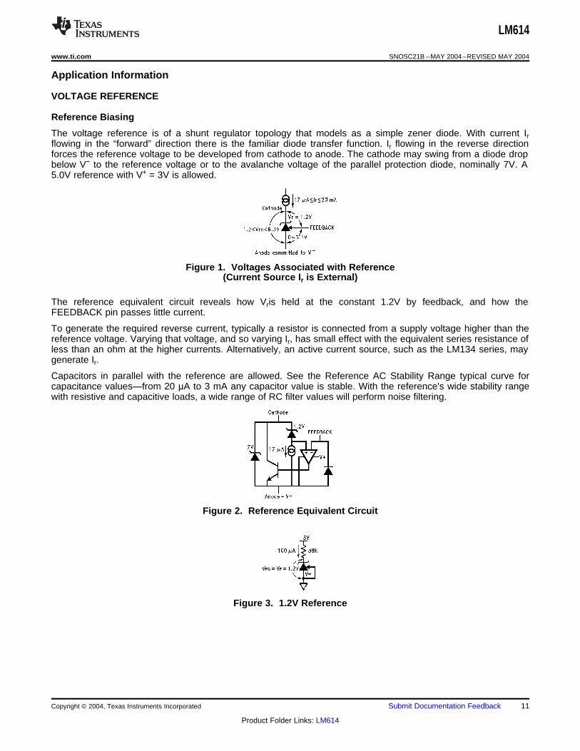
Reference Biasing
The voltage reference is of a shunt regulator topology that models as a simple zener diode. With current Irflowing in the “forward” direction there is the familiar diode transfer function. Ir flowing in the reverse directionforces the reference voltage to be developed from cathode to anode. The cathode may swing from a diode dropbelow V− to the reference voltage or to the avalanche voltage of the parallel protection diode, nominally 7V. A5.0V reference with V+ = 3V is allowed.
Figure 1. Voltages Associated with Reference(Current Source Ir is External)
The reference equivalent circuit reveals how Vris held at the constant 1.2V by feedback, and how theFEEDBACK pin passes little current.
To generate the required reverse current, typically a resistor is connected from a supply voltage higher than thereference voltage. Varying that voltage, and so varying Ir, has small effect with the equivalent series resistance ofless than an ohm at the higher currents. Alternatively, an active current source, such as the LM134 series, maygenerate Ir.
Capacitors in parallel with the reference are allowed. See the Reference AC Stability Range typical curve forcapacitance values—from 20 μA to 3 mA any capacitor value is stable. With the reference's wide stability rangewith resistive and capacitive loads, a wide range of RC filter values will perform noise filtering.
Figure 2. Reference Equivalent Circuit
Figure 3. 1.2V Reference
Copyright © 2004, Texas Instruments Incorporated Submit Documentation Feedback 11
Product Folder Links: LM614
LM614
SNOSC21B –MAY 2004–REVISED MAY 2004 www.ti.com
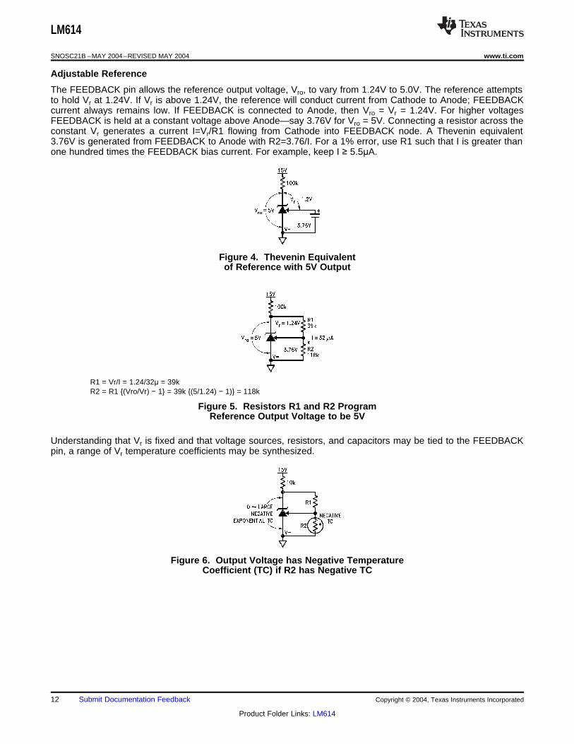
Adjustable Reference
The FEEDBACK pin allows the reference output voltage, Vro, to vary from 1.24V to 5.0V. The reference attemptsto hold Vr at 1.24V. If Vr is above 1.24V, the reference will conduct current from Cathode to Anode; FEEDBACKcurrent always remains low. If FEEDBACK is connected to Anode, then Vro = Vr = 1.24V. For higher voltagesFEEDBACK is held at a constant voltage above Anode—say 3.76V for Vro = 5V. Connecting a resistor across theconstant Vr generates a current I=Vr/R1 flowing from Cathode into FEEDBACK node. A Thevenin equivalent3.76V is generated from FEEDBACK to Anode with R2=3.76/I. For a 1% error, use R1 such that I is greater thanone hundred times the FEEDBACK bias current. For example, keep I ≥ 5.5μA.
Figure 4. Thevenin Equivalentof Reference with 5V Output
R1 = Vr/I = 1.24/32μ = 39kR2 = R1 {(Vro/Vr) − 1} = 39k {(5/1.24) − 1)} = 118k
Figure 5. Resistors R1 and R2 ProgramReference Output Voltage to be 5V
Understanding that Vr is fixed and that voltage sources, resistors, and capacitors may be tied to the FEEDBACKpin, a range of Vr temperature coefficients may be synthesized.
Figure 6. Output Voltage has Negative TemperatureCoefficient (TC) if R2 has Negative TC
12 Submit Documentation Feedback Copyright © 2004, Texas Instruments Incorporated
Product Folder Links: LM614
LM614
www.ti.com SNOSC21B –MAY 2004–REVISED MAY 2004
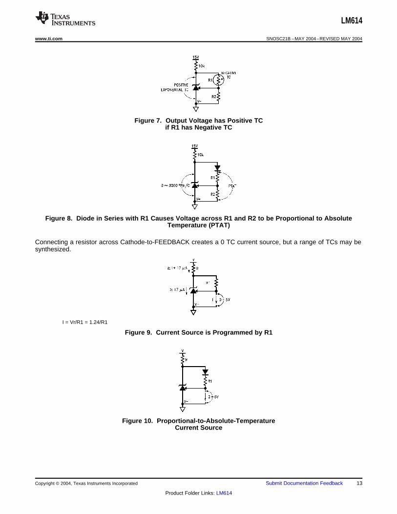
Figure 7. Output Voltage has Positive TCif R1 has Negative TC
Figure 8. Diode in Series with R1 Causes Voltage across R1 and R2 to be Proportional to AbsoluteTemperature (PTAT)
Connecting a resistor across Cathode-to-FEEDBACK creates a 0 TC current source, but a range of TCs may besynthesized.
I = Vr/R1 = 1.24/R1
Figure 9. Current Source is Programmed by R1
Figure 10. Proportional-to-Absolute-TemperatureCurrent Source
Copyright © 2004, Texas Instruments Incorporated Submit Documentation Feedback 13
Product Folder Links: LM614

LM614
SNOSC21B –MAY 2004–REVISED MAY 2004 www.ti.com
Figure 11. Negative-TC Current Source
Hysteresis
The reference voltage depends, slightly, on the thermal history of the die. Competitive micro-power productsvary—always check the data sheet for any given device. Do not assume that no specification means nohysteresis.
OPERATIONAL AMPLIFIERS
Any amp or the reference may be biased in any way with no effect on the other amps or reference, except whena substrate diode conducts (see Guaranteed Electrical Characteristics (1)). One amp input may be outside thecommon-mode range, another amp may be operated as a comparator, another with all terminals floating with noeffect on the others (tying inverting input to output and non-inverting input to V− on unused amps is preferred).Choosing operating points that cause oscillation, such as driving too large a capacitive load, is best avoided.
Op Amp Output Stage
These op amps, like their LM124 series, have flexible and relatively wide-swing output stages. There are simplerules to optimize output swing, reduce cross-over distortion, and optimize capacitive drive capability:1. Output Swing: Unloaded, the 42μA pull-down will bring the output within 300 mV of V− over the military
temperature range. If more than 42μA is required, a resistor from output to V− will help. Swing across anyload may be improved slightly if the load can be tied to V+, at the cost of poorer sinking open-loop voltagegain
2. Cross-over Distortion: The LM614 has lower cross-over distortion (a 1 VBE deadband versus 3 VBE for theLM124), and increased slew rate as shown in the characteristic curves. A resistor pull-up or pull-down willforce class-A operation with only the PNP or NPN output transistor conducting, eliminating cross-overdistortion
3. Capacitive Drive: Limited by the output pole caused by the output resistance driving capacitive loads, a pull-down resistor conducting 1 mA or more reduces the output stage NPN re until the output resistance is that ofthe current limit 25Ω. 200pF may then be driven without oscillation.
Op Amp Input Stage
The lateral PNP input transistors, unlike most op amps, have BVEBO equal to the absolute maximum supplyvoltage. Also, they have no diode clamps to the positive supply nor across the inputs. These features make theinputs look like high impedances to input sources producing large differential and common-mode voltages.
(1) Absolute maximum ratings indicate limits beyond which damage to the component may occur. Electrical specifications do not applywhen operating the device beyond its rated operating conditions.
14 Submit Documentation Feedback Copyright © 2004, Texas Instruments Incorporated
Product Folder Links: LM614

LM614
www.ti.com SNOSC21B –MAY 2004–REVISED MAY 2004
Typical Applications
Figure 12. Simple Low Quiescent Drain Voltage Regulator. Total supply current approximately 320μA,when VIN = +5V.
*10k must be lowt.c. trimpot.
Figure 13. Ultra Low Noise 10.00V Reference. Total output noise is typically 14μVRMS.
VOUT = (R1 /Pe + 1) V REFR1, R2 should be 1% metal filmPβ should be low T.C. trim pot
Figure 14. Slow Rise Time Upon Power-Up, Adjustable Transducer Bridge Driver. Rise time isapproximately 1ms.
Copyright © 2004, Texas Instruments Incorporated Submit Documentation Feedback 15
Product Folder Links: LM614
LM614
SNOSC21B –MAY 2004–REVISED MAY 2004 www.ti.com
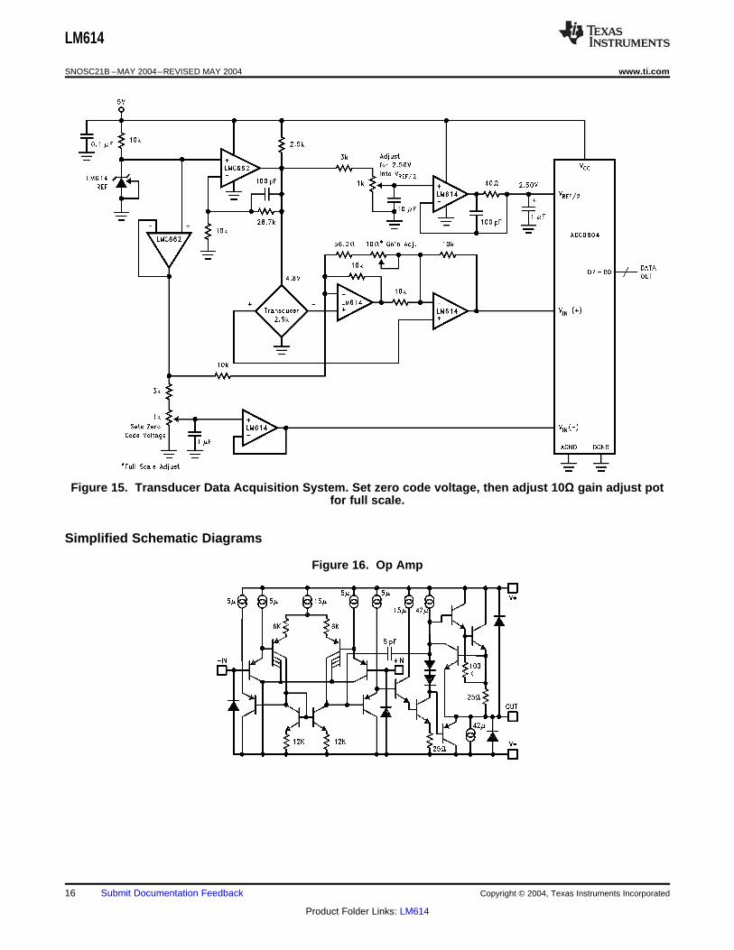
Figure 15. Transducer Data Acquisition System. Set zero code voltage, then adjust 10Ω gain adjust potfor full scale.
Simplified Schematic Diagrams
Figure 16. Op Amp
16 Submit Documentation Feedback Copyright © 2004, Texas Instruments Incorporated
Product Folder Links: LM614
LM614
www.ti.com SNOSC21B –MAY 2004–REVISED MAY 2004
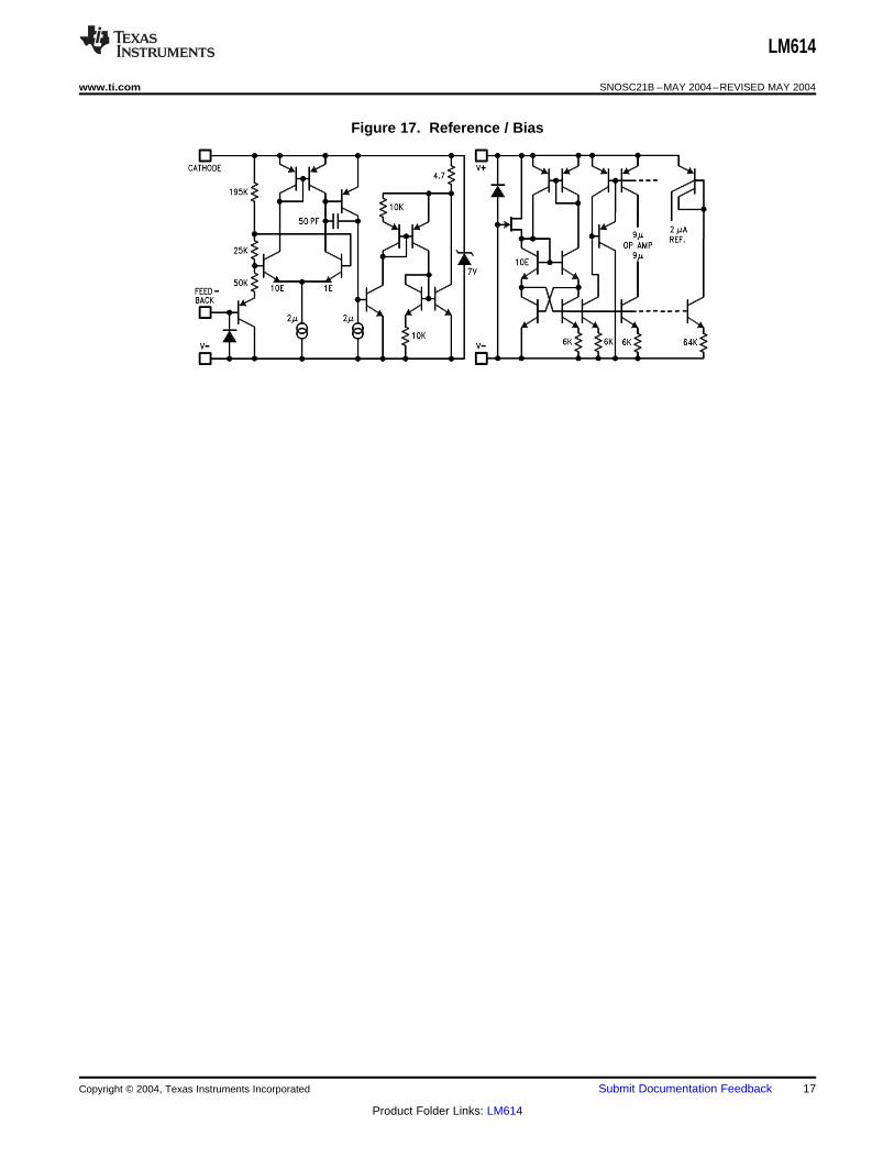
Figure 17. Reference / Bias
Copyright © 2004, Texas Instruments Incorporated Submit Documentation Feedback 17
Product Folder Links: LM614

PACKAGE OPTION ADDENDUM
www.ti.com 17-Nov-2012
Addendum-Page 1
PACKAGING INFORMATION
Orderable Device Status(1)
Package Type PackageDrawing
Pins Package Qty Eco Plan(2)
Lead/Ball Finish MSL Peak Temp(3)
Samples(Requires Login)
LM614CWM/NOPB ACTIVE SOIC DW 16 45 Green (RoHS& no Sb/Br)
CU SN Level-3-260C-168 HR
LM614IWM ACTIVE SOIC DW 16 45 TBD CU SNPB Level-2A-220C-4WEEK
LM614IWM/NOPB ACTIVE SOIC DW 16 45 Green (RoHS& no Sb/Br)
CU SN Level-3-260C-168 HR
LM614IWMX ACTIVE SOIC DW 16 1000 TBD CU SNPB Level-2A-220C-4WEEK
LM614IWMX/NOPB ACTIVE SOIC DW 16 1000 Green (RoHS& no Sb/Br)
CU SN Level-3-260C-168 HR
(1) The marketing status values are defined as follows:ACTIVE: Product device recommended for new designs.LIFEBUY: TI has announced that the device will be discontinued, and a lifetime-buy period is in effect.NRND: Not recommended for new designs. Device is in production to support existing customers, but TI does not recommend using this part in a new design.PREVIEW: Device has been announced but is not in production. Samples may or may not be available.OBSOLETE: TI has discontinued the production of the device.
(2) Eco Plan - The planned eco-friendly classification: Pb-Free (RoHS), Pb-Free (RoHS Exempt), or Green (RoHS & no Sb/Br) - please check http://www.ti.com/productcontent for the latest availabilityinformation and additional product content details.TBD: The Pb-Free/Green conversion plan has not been defined.Pb-Free (RoHS): TI's terms "Lead-Free" or "Pb-Free" mean semiconductor products that are compatible with the current RoHS requirements for all 6 substances, including the requirement thatlead not exceed 0.1% by weight in homogeneous materials. Where designed to be soldered at high temperatures, TI Pb-Free products are suitable for use in specified lead-free processes.Pb-Free (RoHS Exempt): This component has a RoHS exemption for either 1) lead-based flip-chip solder bumps used between the die and package, or 2) lead-based die adhesive used betweenthe die and leadframe. The component is otherwise considered Pb-Free (RoHS compatible) as defined above.Green (RoHS & no Sb/Br): TI defines "Green" to mean Pb-Free (RoHS compatible), and free of Bromine (Br) and Antimony (Sb) based flame retardants (Br or Sb do not exceed 0.1% by weightin homogeneous material)
(3) MSL, Peak Temp. -- The Moisture Sensitivity Level rating according to the JEDEC industry standard classifications, and peak solder temperature.
Important Information and Disclaimer:The information provided on this page represents TI's knowledge and belief as of the date that it is provided. TI bases its knowledge and belief on informationprovided by third parties, and makes no representation or warranty as to the accuracy of such information. Efforts are underway to better integrate information from third parties. TI has taken andcontinues to take reasonable steps to provide representative and accurate information but may not have conducted destructive testing or chemical analysis on incoming materials and chemicals.TI and TI suppliers consider certain information to be proprietary, and thus CAS numbers and other limited information may not be available for release.
In no event shall TI's liability arising out of such information exceed the total purchase price of the TI part(s) at issue in this document sold by TI to Customer on an annual basis.

PACKAGE OPTION ADDENDUM
www.ti.com 17-Nov-2012
Addendum-Page 2

TAPE AND REEL INFORMATION
*All dimensions are nominal
Device PackageType
PackageDrawing
Pins SPQ ReelDiameter
(mm)
ReelWidth
W1 (mm)
A0(mm)
B0(mm)
K0(mm)
P1(mm)
W(mm)
Pin1Quadrant
LM614IWMX SOIC DW 16 1000 330.0 16.4 10.9 10.7 3.2 12.0 16.0 Q1
LM614IWMX/NOPB SOIC DW 16 1000 330.0 16.4 10.9 10.7 3.2 12.0 16.0 Q1
PACKAGE MATERIALS INFORMATION
www.ti.com 17-Nov-2012
Pack Materials-Page 1

*All dimensions are nominal
Device Package Type Package Drawing Pins SPQ Length (mm) Width (mm) Height (mm)
LM614IWMX SOIC DW 16 1000 358.0 343.0 63.0
LM614IWMX/NOPB SOIC DW 16 1000 358.0 343.0 63.0
PACKAGE MATERIALS INFORMATION
www.ti.com 17-Nov-2012
Pack Materials-Page 2

IMPORTANT NOTICE
Texas Instruments Incorporated and its subsidiaries (TI) reserve the right to make corrections, enhancements, improvements and otherchanges to its semiconductor products and services per JESD46, latest issue, and to discontinue any product or service per JESD48, latestissue. Buyers should obtain the latest relevant information before placing orders and should verify that such information is current andcomplete. All semiconductor products (also referred to herein as “components”) are sold subject to TI’s terms and conditions of salesupplied at the time of order acknowledgment.
TI warrants performance of its components to the specifications applicable at the time of sale, in accordance with the warranty in TI’s termsand conditions of sale of semiconductor products. Testing and other quality control techniques are used to the extent TI deems necessaryto support this warranty. Except where mandated by applicable law, testing of all parameters of each component is not necessarilyperformed.
TI assumes no liability for applications assistance or the design of Buyers’ products. Buyers are responsible for their products andapplications using TI components. To minimize the risks associated with Buyers’ products and applications, Buyers should provideadequate design and operating safeguards.
TI does not warrant or represent that any license, either express or implied, is granted under any patent right, copyright, mask work right, orother intellectual property right relating to any combination, machine, or process in which TI components or services are used. Informationpublished by TI regarding third-party products or services does not constitute a license to use such products or services or a warranty orendorsement thereof. Use of such information may require a license from a third party under the patents or other intellectual property of thethird party, or a license from TI under the patents or other intellectual property of TI.
Reproduction of significant portions of TI information in TI data books or data sheets is permissible only if reproduction is without alterationand is accompanied by all associated warranties, conditions, limitations, and notices. TI is not responsible or liable for such altereddocumentation. Information of third parties may be subject to additional restrictions.
Resale of TI components or services with statements different from or beyond the parameters stated by TI for that component or servicevoids all express and any implied warranties for the associated TI component or service and is an unfair and deceptive business practice.TI is not responsible or liable for any such statements.
Buyer acknowledges and agrees that it is solely responsible for compliance with all legal, regulatory and safety-related requirementsconcerning its products, and any use of TI components in its applications, notwithstanding any applications-related information or supportthat may be provided by TI. Buyer represents and agrees that it has all the necessary expertise to create and implement safeguards whichanticipate dangerous consequences of failures, monitor failures and their consequences, lessen the likelihood of failures that might causeharm and take appropriate remedial actions. Buyer will fully indemnify TI and its representatives against any damages arising out of the useof any TI components in safety-critical applications.
In some cases, TI components may be promoted specifically to facilitate safety-related applications. With such components, TI’s goal is tohelp enable customers to design and create their own end-product solutions that meet applicable functional safety standards andrequirements. Nonetheless, such components are subject to these terms.
No TI components are authorized for use in FDA Class III (or similar life-critical medical equipment) unless authorized officers of the partieshave executed a special agreement specifically governing such use.
Only those TI components which TI has specifically designated as military grade or “enhanced plastic” are designed and intended for use inmilitary/aerospace applications or environments. Buyer acknowledges and agrees that any military or aerospace use of TI componentswhich have not been so designated is solely at the Buyer's risk, and that Buyer is solely responsible for compliance with all legal andregulatory requirements in connection with such use.
TI has specifically designated certain components as meeting ISO/TS16949 requirements, mainly for automotive use. In any case of use ofnon-designated products, TI will not be responsible for any failure to meet ISO/TS16949.
Products Applications
Audio www.ti.com/audio Automotive and Transportation www.ti.com/automotive
Amplifiers amplifier.ti.com Communications and Telecom www.ti.com/communications
Data Converters dataconverter.ti.com Computers and Peripherals www.ti.com/computers
DLP® Products www.dlp.com Consumer Electronics www.ti.com/consumer-apps
DSP dsp.ti.com Energy and Lighting www.ti.com/energy
Clocks and Timers www.ti.com/clocks Industrial www.ti.com/industrial
Interface interface.ti.com Medical www.ti.com/medical
Logic logic.ti.com Security www.ti.com/security
Power Mgmt power.ti.com Space, Avionics and Defense www.ti.com/space-avionics-defense
Microcontrollers microcontroller.ti.com Video and Imaging www.ti.com/video
RFID www.ti-rfid.com
OMAP Applications Processors www.ti.com/omap TI E2E Community e2e.ti.com
Wireless Connectivity www.ti.com/wirelessconnectivity
Mailing Address: Texas Instruments, Post Office Box 655303, Dallas, Texas 75265Copyright © 2012, Texas Instruments Incorporated
Mouser Electronics
Authorized Distributor
Click to View Pricing, Inventory, Delivery & Lifecycle Information: Texas Instruments:
LM614CWM LM614CWM/NOPB LM614IWM LM614IWM/NOPB LM614IWMX LM614IWMX/NOPB