lm231b52ebad10ee97eea25d5e-d7d40819259e7d3022d9ad53e3694148.r84.cf… · lm231b - 2323 middle power...
TRANSCRIPT
http://www.samsungled.com 1 / 49
Rev:
Product Family Data Sheet
SAMSUNG ELECTRONICS
95, Samsung2-Ro, Giheung-Gu,
Yongin-City, Gyeonggi-Do 446-711, KOREA
ISSUE NO : 002
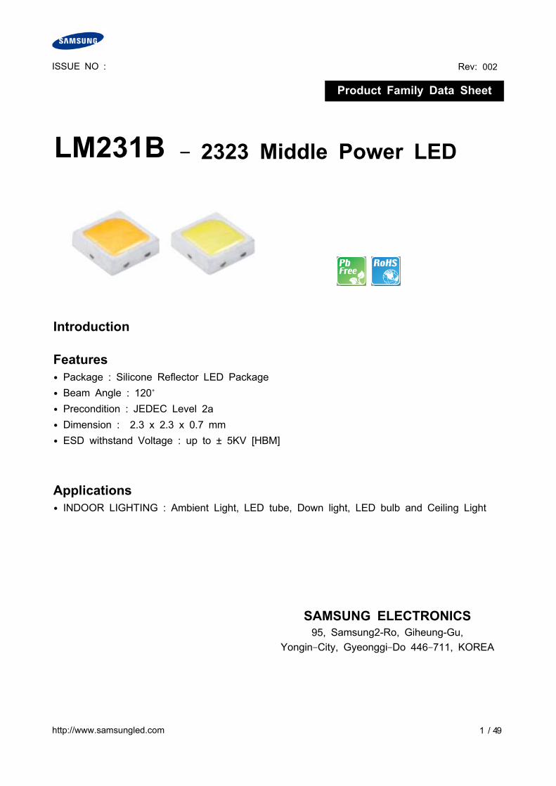
LM231B - 2323 Middle Power LED
Introduction
Features
Package : Silicone Reflector LED Package
Beam Angle : 120˚
Precondition : JEDEC Level 2a
Dimension : 2.3 x 2.3 x 0.7 mm
ESD withstand Voltage : up to ± 5KV [HBM]
Reliability Test : LM-80 qualified
Applications
INDOOR LIGHTING : Ambient Light, LED tube, Down light, LED bulb and Ceiling Light
http://www.samsungled.com 2 / 49
Contents
1. Product Code Information ----------------------- 3
2. Luminous Flux Characteristics ----------------------- 10
3. Characteristics ----------------------- 12
4. Typical Characteristics Graph ----------------------- 13
5. Outline Drawing & Dimension ----------------------- 19
6. Reliability Test Items & Conditions ----------------------- 20
7. Solder Conditions ----------------------- 21
8. Tape & Reel ----------------------- 22
9. Label Structure ----------------------- 23
10. Packing Structure ----------------------- 24
11. Precaution For Use ----------------------- 26
12. Hazard Substance Analysis Report ----------------------- 29
http://www.samsungled.com 3 / 49
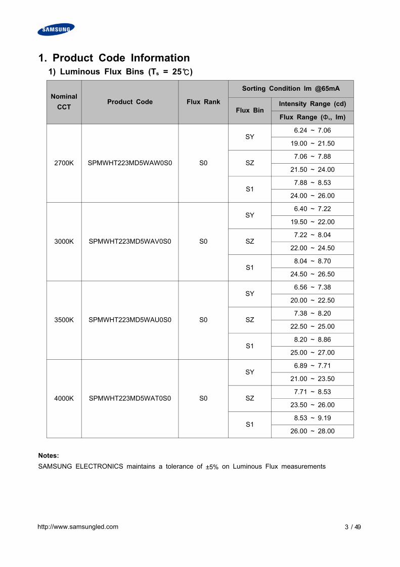
1. Product Code Information
1) Luminous Flux Bins (Ts = 25)
Nominal
CCTProduct Code Flux Rank
Sorting Condition lm @65mA
Flux BinIntensity Range (cd)
Flux Range (Φv, lm)
2700K SPMWHT223MD5WAW0S0 S0
SY6.24 ~ 7.06
19.00 ~ 21.50
SZ7.06 ~ 7.88
21.50 ~ 24.00
S17.88 ~ 8.53
24.00 ~ 26.00
3000K SPMWHT223MD5WAV0S0 S0
SY6.40 ~ 7.22
19.50 ~ 22.00
SZ7.22 ~ 8.04
22.00 ~ 24.50
S18.04 ~ 8.70
24.50 ~ 26.50
3500K SPMWHT223MD5WAU0S0 S0
SY6.56 ~ 7.38
20.00 ~ 22.50
SZ7.38 ~ 8.20
22.50 ~ 25.00
S18.20 ~ 8.86
25.00 ~ 27.00
4000K SPMWHT223MD5WAT0S0 S0
SY6.89 ~ 7.71
21.00 ~ 23.50
SZ7.71 ~ 8.53
23.50 ~ 26.00
S18.53 ~ 9.19
26.00 ~ 28.00
Notes:
SAMSUNG ELECTRONICS maintains a tolerance of ±5% on Luminous Flux measurements
http://www.samsungled.com 4 / 49
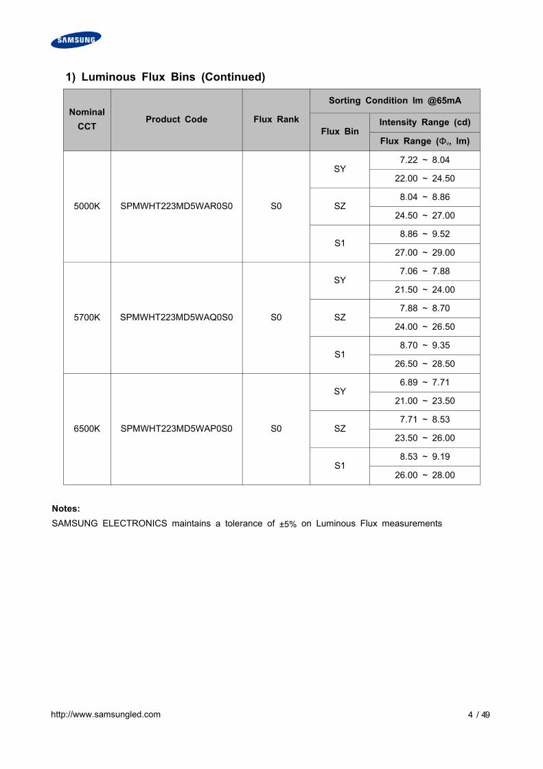
1) Luminous Flux Bins (Continued)
Nominal
CCTProduct Code Flux Rank
Sorting Condition lm @65mA
Flux BinIntensity Range (cd)
Flux Range (Φv, lm)
5000K SPMWHT223MD5WAR0S0 S0
SY7.22 ~ 8.04
22.00 ~ 24.50
SZ8.04 ~ 8.86
24.50 ~ 27.00
S18.86 ~ 9.52
27.00 ~ 29.00
5700K SPMWHT223MD5WAQ0S0 S0
SY7.06 ~ 7.88
21.50 ~ 24.00
SZ7.88 ~ 8.70
24.00 ~ 26.50
S18.70 ~ 9.35
26.50 ~ 28.50
6500K SPMWHT223MD5WAP0S0 S0
SY6.89 ~ 7.71
21.00 ~ 23.50
SZ7.71 ~ 8.53
23.50 ~ 26.00
S18.53 ~ 9.19
26.00 ~ 28.00
Notes:
SAMSUNG ELECTRONICS maintains a tolerance of ±5% on Luminous Flux measurements

http://www.samsungled.com 5 / 49
2) Color Bins (Ts = 25)
1) Color Binning
Nominal
CCTProduct Code Color Rank Chromaticity Bins
2700K SPMWHT223MD5WAW0S0 W0(Whole bin)W1, W2, W3, W4, W5, W6, W7, W8,
W9, WA, WB, WC, WD, WE, WF, WG
3000K SPMWHT223MD5WAV0S0 V0(Whole bin)V1, V2, V3, V4, V5, V6, V7, V8,
V9, VA, VB, VC, VD, VE, VF, VG
3500K SPMWHT223MD5WAU0S0 U0(Whole bin)U1, U2, U3, U4, U5, U6, U7, U8,
U9, UA, UB, UC, UD, UE, UF, UG
4000K SPMWHT223MD5WAT0S0 T0(Whole bin)T1, T2, T3, T4, T5, T6, T7, T8,
T9, TA, TB, TC, TD, TE, TF, TG
5000K SPMWHT223MD5WAR0S0 R0(Whole bin) R1, R2, R3, R4, R5, R6, R7, R8
5700K SPMWHT223MD5WAQ0S0 Q0(Whole bin) Q1, Q2, Q3, Q4, Q5, Q6, Q7, Q8
6500K SPMWHT223MD5WAP0S0 P0(Whole bin) P1, P2, P3, P4, P5, P6, P7, P8
http://www.samsungled.com 6 / 49
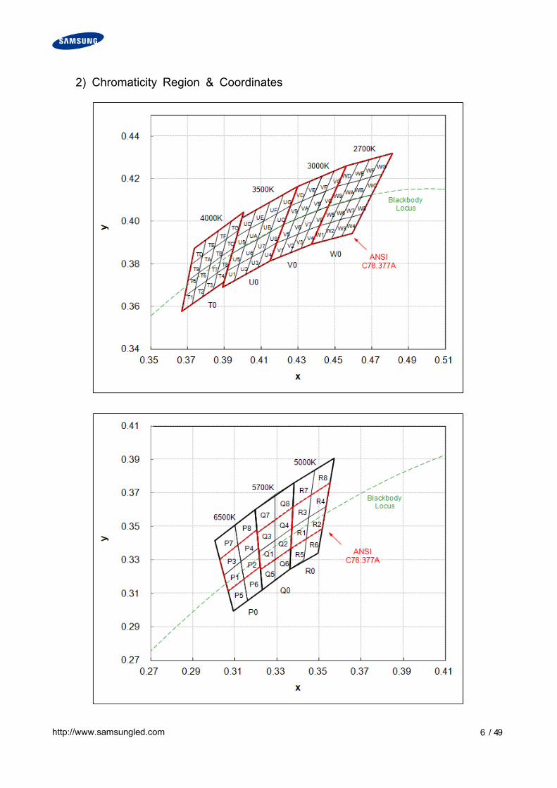
2) Chromaticity Region & Coordinates
http://www.samsungled.com 7 / 49
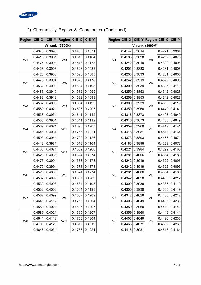
2) Chromaticity Region & Coordinates (Continued)
Region CIE X CIE Y Region CIE X CIE Y
V rank (3000K)
V1
0.4147 0.3814
V9
0.4221 0.3984
0.4183 0.3898 0.4259 0.4073
0.4242 0.3919 0.4322 0.4096
0.4203 0.3833 0.4281 0.4006
V2
0.4203 0.3833
VA
0.4281 0.4006
0.4242 0.3919 0.4322 0.4096
0.4300 0.3939 0.4385 0.4119
0.4259 0.3853 0.4342 0.4028
V3
0.4259 0.3853
VB
0.4342 0.4028
0.4300 0.3939 0.4385 0.4119
0.4359 0.3960 0.4449 0.4141
0.4316 0.3873 0.4403 0.4049
V4
0.4316 0.3873
VC
0.4403 0.4049
0.4359 0.3960 0.4449 0.4141
0.4418 0.3981 0.4513 0.4164
0.4373 0.3893 0.4465 0.4071
V5
0.4183 0.3898
VD
0.4259 0.4073
0.4221 0.3984 0.4299 0.4165
0.4281 0.4006 0.4364 0.4188
0.4242 0.3919 0.4322 0.4096
V6
0.4242 0.3919
VE
0.4322 0.4096
0.4281 0.4006 0.4364 0.4188
0.4342 0.4028 0.4430 0.4212
0.4300 0.3939 0.4385 0.4119
V7
0.4300 0.3939
VF
0.4385 0.4119
0.4342 0.4028 0.4430 0.4212
0.4403 0.4049 0.4496 0.4236
0.4359 0.3960 0.4449 0.4141
V8
0.4359 0.3960
VG
0.4449 0.4141
0.4403 0.4049 0.4496 0.4236
0.4465 0.4071 0.4562 0.4260
0.4418 0.3981 0.4513 0.4164
Region CIE X CIE Y Region CIE X CIE Y
W rank (2700K)
W1
0.4373 0.3893
W9
0.4465 0.4071
0.4418 0.3981 0.4513 0.4164
0.4475 0.3994 0.4573 0.4178
0.4428 0.3906 0.4523 0.4085
W2
0.4428 0.3906
WA
0.4523 0.4085
0.4475 0.3994 0.4573 0.4178
0.4532 0.4008 0.4634 0.4193
0.4483 0.3919 0.4582 0.4099
W3
0.4483 0.3919
WB
0.4582 0.4099
0.4532 0.4008 0.4634 0.4193
0.4589 0.4021 0.4695 0.4207
0.4538 0.3931 0.4641 0.4112
W4
0.4538 0.3931
WC
0.4641 0.4112
0.4589 0.4021 0.4695 0.4207
0.4646 0.4034 0.4756 0.4221
0.4593 0.3944 0.4700 0.4126
W5
0.4418 0.3981
WD
0.4513 0.4164
0.4465 0.4071 0.4562 0.4260
0.4523 0.4085 0.4624 0.4274
0.4475 0.3994 0.4573 0.4178
W6
0.4475 0.3994
WE
0.4573 0.4178
0.4523 0.4085 0.4624 0.4274
0.4582 0.4099 0.4687 0.4289
0.4532 0.4008 0.4634 0.4193
W7
0.4532 0.4008
WF
0.4634 0.4193
0.4582 0.4099 0.4687 0.4289
0.4641 0.4112 0.4750 0.4304
0.4589 0.4021 0.4695 0.4207
W8
0.4589 0.4021
WG
0.4695 0.4207
0.4641 0.4112 0.4750 0.4304
0.4700 0.4126 0.4813 0.4319
0.4646 0.4034 0.4756 0.4221
http://www.samsungled.com 8 / 49
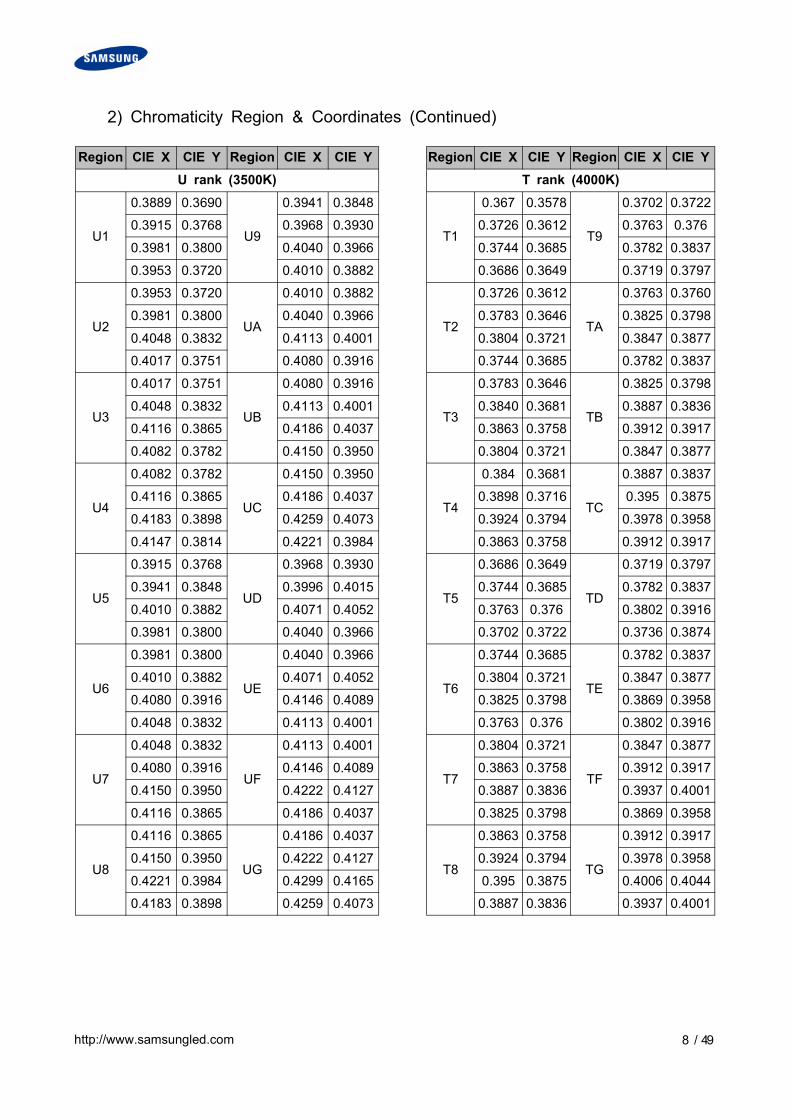
2) Chromaticity Region & Coordinates (Continued)
Region CIE X CIE Y Region CIE X CIE Y
T rank (4000K)
T1
0.367 0.3578
T9
0.3702 0.3722
0.3726 0.3612 0.3763 0.376
0.3744 0.3685 0.3782 0.3837
0.3686 0.3649 0.3719 0.3797
T2
0.3726 0.3612
TA
0.3763 0.3760
0.3783 0.3646 0.3825 0.3798
0.3804 0.3721 0.3847 0.3877
0.3744 0.3685 0.3782 0.3837
T3
0.3783 0.3646
TB
0.3825 0.3798
0.3840 0.3681 0.3887 0.3836
0.3863 0.3758 0.3912 0.3917
0.3804 0.3721 0.3847 0.3877
T4
0.384 0.3681
TC
0.3887 0.3837
0.3898 0.3716 0.395 0.3875
0.3924 0.3794 0.3978 0.3958
0.3863 0.3758 0.3912 0.3917
T5
0.3686 0.3649
TD
0.3719 0.3797
0.3744 0.3685 0.3782 0.3837
0.3763 0.376 0.3802 0.3916
0.3702 0.3722 0.3736 0.3874
T6
0.3744 0.3685
TE
0.3782 0.3837
0.3804 0.3721 0.3847 0.3877
0.3825 0.3798 0.3869 0.3958
0.3763 0.376 0.3802 0.3916
T7
0.3804 0.3721
TF
0.3847 0.3877
0.3863 0.3758 0.3912 0.3917
0.3887 0.3836 0.3937 0.4001
0.3825 0.3798 0.3869 0.3958
T8
0.3863 0.3758
TG
0.3912 0.3917
0.3924 0.3794 0.3978 0.3958
0.395 0.3875 0.4006 0.4044
0.3887 0.3836 0.3937 0.4001
Region CIE X CIE Y Region CIE X CIE Y
U rank (3500K)
U1
0.3889 0.3690
U9
0.3941 0.3848
0.3915 0.3768 0.3968 0.3930
0.3981 0.3800 0.4040 0.3966
0.3953 0.3720 0.4010 0.3882
U2
0.3953 0.3720
UA
0.4010 0.3882
0.3981 0.3800 0.4040 0.3966
0.4048 0.3832 0.4113 0.4001
0.4017 0.3751 0.4080 0.3916
U3
0.4017 0.3751
UB
0.4080 0.3916
0.4048 0.3832 0.4113 0.4001
0.4116 0.3865 0.4186 0.4037
0.4082 0.3782 0.4150 0.3950
U4
0.4082 0.3782
UC
0.4150 0.3950
0.4116 0.3865 0.4186 0.4037
0.4183 0.3898 0.4259 0.4073
0.4147 0.3814 0.4221 0.3984
U5
0.3915 0.3768
UD
0.3968 0.3930
0.3941 0.3848 0.3996 0.4015
0.4010 0.3882 0.4071 0.4052
0.3981 0.3800 0.4040 0.3966
U6
0.3981 0.3800
UE
0.4040 0.3966
0.4010 0.3882 0.4071 0.4052
0.4080 0.3916 0.4146 0.4089
0.4048 0.3832 0.4113 0.4001
U7
0.4048 0.3832
UF
0.4113 0.4001
0.4080 0.3916 0.4146 0.4089
0.4150 0.3950 0.4222 0.4127
0.4116 0.3865 0.4186 0.4037
U8
0.4116 0.3865
UG
0.4186 0.4037
0.4150 0.3950 0.4222 0.4127
0.4221 0.3984 0.4299 0.4165
0.4183 0.3898 0.4259 0.4073
http://www.samsungled.com 9 / 49
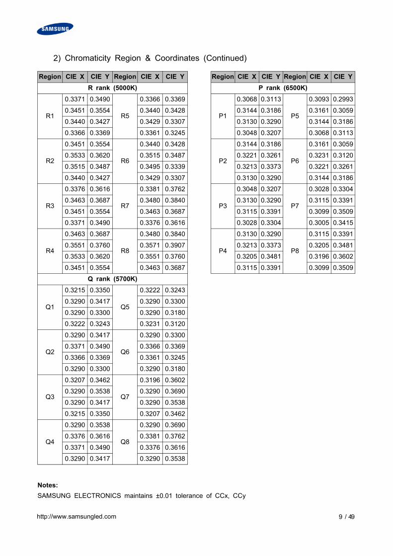
2) Chromaticity Region & Coordinates (Continued)
Notes:
SAMSUNG ELECTRONICS maintains ±0.01 tolerance of CCx, CCy
Region CIE X CIE Y Region CIE X CIE Y
P rank (6500K)
P1
0.3068 0.3113
P5
0.3093 0.2993
0.3144 0.3186 0.3161 0.3059
0.3130 0.3290 0.3144 0.3186
0.3048 0.3207 0.3068 0.3113
P2
0.3144 0.3186
P6
0.3161 0.3059
0.3221 0.3261 0.3231 0.3120
0.3213 0.3373 0.3221 0.3261
0.3130 0.3290 0.3144 0.3186
P3
0.3048 0.3207
P7
0.3028 0.3304
0.3130 0.3290 0.3115 0.3391
0.3115 0.3391 0.3099 0.3509
0.3028 0.3304 0.3005 0.3415
P4
0.3130 0.3290
P8
0.3115 0.3391
0.3213 0.3373 0.3205 0.3481
0.3205 0.3481 0.3196 0.3602
0.3115 0.3391 0.3099 0.3509
Region CIE X CIE Y Region CIE X CIE Y
R rank (5000K)
R1
0.3371 0.3490
R5
0.3366 0.3369
0.3451 0.3554 0.3440 0.3428
0.3440 0.3427 0.3429 0.3307
0.3366 0.3369 0.3361 0.3245
R2
0.3451 0.3554
R6
0.3440 0.3428
0.3533 0.3620 0.3515 0.3487
0.3515 0.3487 0.3495 0.3339
0.3440 0.3427 0.3429 0.3307
R3
0.3376 0.3616
R7
0.3381 0.3762
0.3463 0.3687 0.3480 0.3840
0.3451 0.3554 0.3463 0.3687
0.3371 0.3490 0.3376 0.3616
R4
0.3463 0.3687
R8
0.3480 0.3840
0.3551 0.3760 0.3571 0.3907
0.3533 0.3620 0.3551 0.3760
0.3451 0.3554 0.3463 0.3687
Q rank (5700K)
Q1
0.3215 0.3350
Q5
0.3222 0.3243
0.3290 0.3417 0.3290 0.3300
0.3290 0.3300 0.3290 0.3180
0.3222 0.3243 0.3231 0.3120
Q2
0.3290 0.3417
Q6
0.3290 0.3300
0.3371 0.3490 0.3366 0.3369
0.3366 0.3369 0.3361 0.3245
0.3290 0.3300 0.3290 0.3180
Q3
0.3207 0.3462
Q7
0.3196 0.3602
0.3290 0.3538 0.3290 0.3690
0.3290 0.3417 0.3290 0.3538
0.3215 0.3350 0.3207 0.3462
Q4
0.3290 0.3538
Q8
0.3290 0.3690
0.3376 0.3616 0.3381 0.3762
0.3371 0.3490 0.3376 0.3616
0.3290 0.3417 0.3290 0.3538

http://www.samsungled.com 10 / 49
2. Luminous Flux Characteristics (Ts = 25)
Nominal
CCT
Minimum
CRIIf(mA) Vf(V) Power(W) Flux(lm) lm/W
2700K 80
50 2.85 0.14 16.3 114
60 2.88 0.17 19.4 112
65 2.91 0.19 20.9 110
70 2.94 0.21 22.4 109
80 2.97 0.24 25.1 106
90 3.00 0.27 27.6 102
100 3.03 0.30 30.3 100
150 3.14 0.47 41.8 89
3000K 80
50 2.85 0.14 16.8 118
60 2.88 0.17 20.1 116
65 2.91 0.19 21.6 114
70 2.94 0.21 23.1 112
80 2.97 0.24 25.9 109
90 3.00 0.27 28.5 106
100 3.03 0.30 31.3 103
150 3.14 0.47 43.2 92
3500K 80
50 2.85 0.14 17.6 124
60 2.88 0.17 21.0 122
65 2.91 0.19 22.6 119
70 2.94 0.21 24.2 118
80 2.97 0.24 27.1 114
90 3.00 0.27 29.8 111
100 3.03 0.30 32.8 108
150 3.14 0.47 45.2 96
4000K 80
50 2.85 0.14 18.3 129
60 2.88 0.17 21.9 126
65 2.91 0.19 23.5 124
70 2.94 0.21 25.1 122
80 2.97 0.24 28.2 119
90 3.00 0.27 31.0 115
100 3.03 0.30 34.1 113
150 3.14 0.47 47.0 100
Notes:
Luminous Flux(Φv, lm) values are for representative reference only

http://www.samsungled.com 11 / 49
2. Luminous Flux Characteristics (Ts = 25)
Nominal
CCT
Minimum
CRIIf(mA) Vf(V) Power(W) Flux(lm) lm/W
5000K 80
50 2.85 0.14 18.7 131
60 2.88 0.17 22.3 129
65 2.91 0.19 24.0 127
70 2.94 0.21 25.7 125
80 2.97 0.24 28.8 121
90 3.00 0.27 31.7 117
100 3.03 0.30 34.8 115
150 3.14 0.47 48.0 102
5700K 80
50 2.85 0.14 18.2 127
60 2.88 0.17 21.7 125
65 2.91 0.19 23.3 123
70 2.94 0.21 24.9 121
80 2.97 0.24 28.0 118
90 3.00 0.27 30.8 114
100 3.03 0.30 33.8 112
150 3.14 0.47 46.6 99
6500K 80
50 2.85 0.14 17.9 126
60 2.88 0.17 21.4 124
65 2.91 0.19 23.0 122
70 2.94 0.21 24.6 120
80 2.97 0.24 27.6 116
90 3.00 0.27 30.4 113
100 3.03 0.30 33.4 110
150 3.14 0.47 46.0 98
Notes:
Luminous Flux(Φv, lm) values are for representative reference only
http://www.samsungled.com 12 / 49
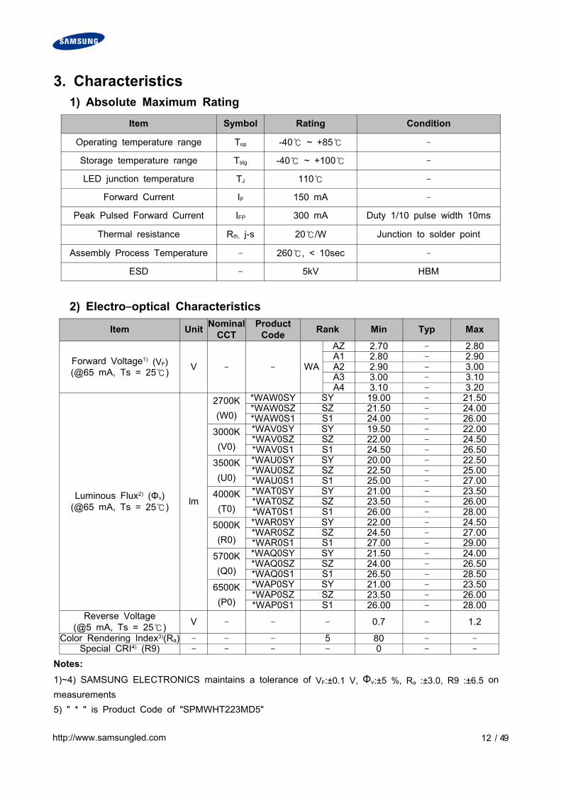
3. Characteristics
1) Absolute Maximum Rating
Item Symbol Rating Condition
Operating temperature range Top -40 ~ +85 -
Storage temperature range Tstg -40 ~ +100 -
LED junction temperature TJ 110 -
Forward Current IF 150 mA -
Peak Pulsed Forward Current IFP 300 mA Duty 1/10 pulse width 10ms
Thermal resistance Rth, j-s 20/W Junction to solder point
Assembly Process Temperature - 260, < 10sec -
ESD - 5kV HBM
2) Electro-optical Characteristics
Item UnitNominal
CCT
Product
CodeRank Min Typ Max
Forward Voltage1) (VF)(@65 mA, Ts = 25)
V - - WA
AZ 2.70 - 2.80A1 2.80 - 2.90A2 2.90 - 3.00A3 3.00 - 3.10A4 3.10 - 3.20
Luminous Flux2) (Φv)
(@65 mA, Ts = 25)lm
2700K
(W0)
*WAW0SY SY 19.00 - 21.50*WAW0SZ SZ 21.50 - 24.00*WAW0S1 S1 24.00 - 26.00
3000K
(V0)
*WAV0SY SY 19.50 - 22.00*WAV0SZ SZ 22.00 - 24.50*WAV0S1 S1 24.50 - 26.50
3500K
(U0)
*WAU0SY SY 20.00 - 22.50*WAU0SZ SZ 22.50 - 25.00*WAU0S1 S1 25.00 - 27.00
4000K
(T0)
*WAT0SY SY 21.00 - 23.50*WAT0SZ SZ 23.50 - 26.00*WAT0S1 S1 26.00 - 28.00
5000K
(R0)
*WAR0SY SY 22.00 - 24.50*WAR0SZ SZ 24.50 - 27.00*WAR0S1 S1 27.00 - 29.00
5700K
(Q0)
*WAQ0SY SY 21.50 - 24.00*WAQ0SZ SZ 24.00 - 26.50*WAQ0S1 S1 26.50 - 28.50
6500K
(P0)
*WAP0SY SY 21.00 - 23.50*WAP0SZ SZ 23.50 - 26.00*WAP0S1 S1 26.00 - 28.00
Reverse Voltage
(@5 mA, Ts = 25)V - - - 0.7 - 1.2
Color Rendering Index3)(Ra) - - - 5 80 - -Special CRI4) (R9) - - - - 0 - -
Notes:
1)~4) SAMSUNG ELECTRONICS maintains a tolerance of VF:±0.1 V, Φv:±5 %, Ra :±3.0, R9 :±6.5 on
measurements
5) " * " is Product Code of "SPMWHT223MD5"

http://www.samsungled.com 13 / 49
4. Typical Characteristics Graph (@65mA, Ts = 25)
1) Spectrum Distribution
[CCT : 2700K & 3000K]
[CCT : 3500K & 4000K]

http://www.samsungled.com 14 / 49
[CCT : 5000K]
[CCT : 5700K~6500K]
http://www.samsungled.com 15 / 49
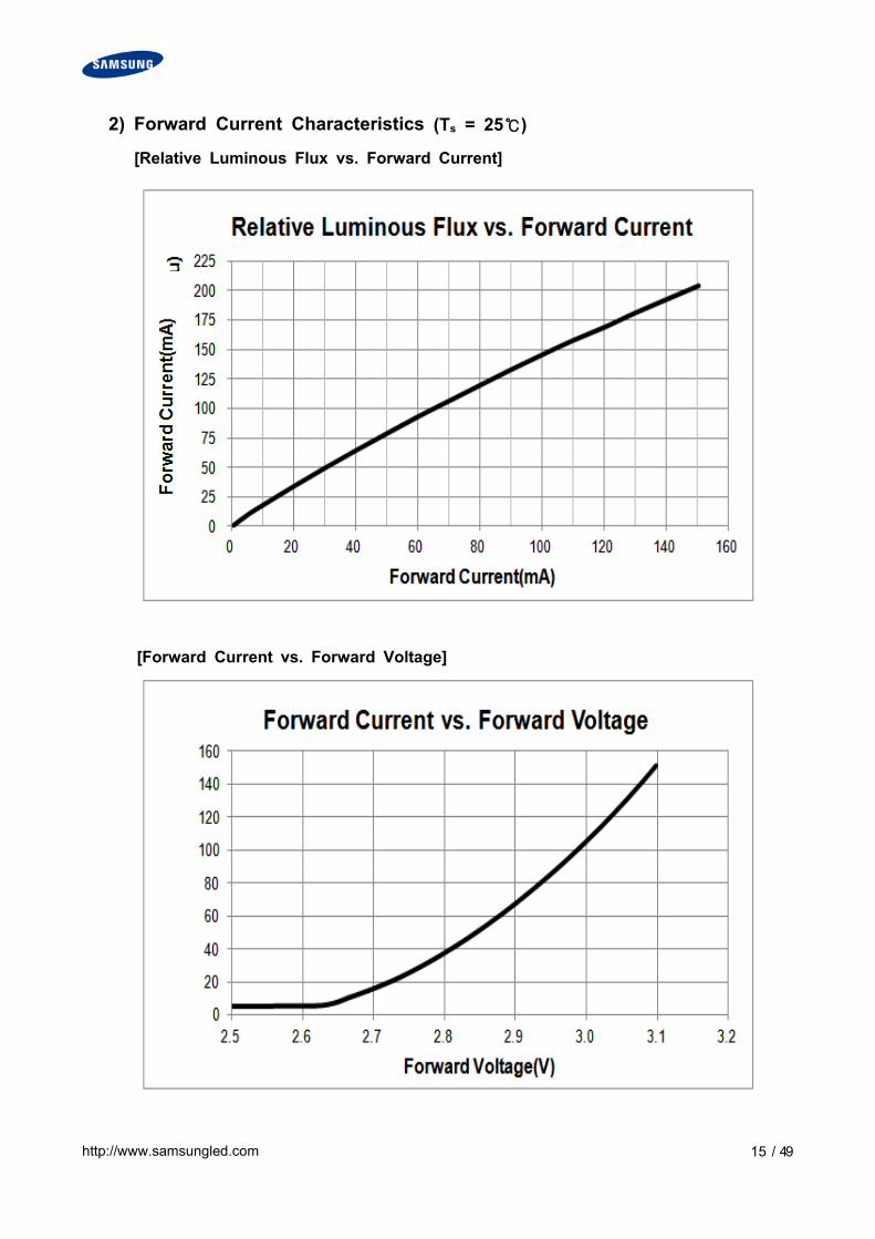
2) Forward Current Characteristics (Ts = 25)
[Relative Luminous Flux vs. Forward Current]
[Forward Current vs. Forward Voltage]
http://www.samsungled.com 16 / 49
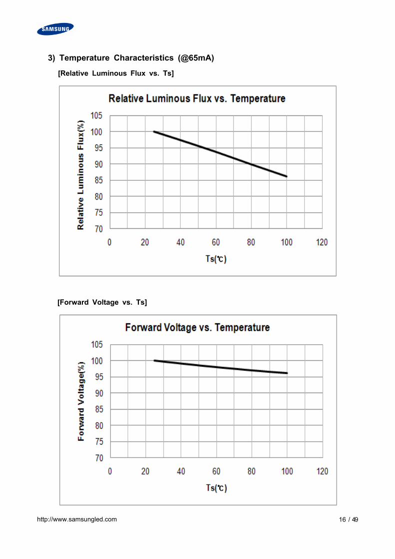
3) Temperature Characteristics (@65mA)
[Relative Luminous Flux vs. Ts]
[Forward Voltage vs. Ts]

http://www.samsungled.com 17 / 49
[Color x, y vs. Ts]
4) Color shift Characteristics (Ts = 25)
[Forward Current vs. Color x, y]

http://www.samsungled.com 18 / 49
5) Derating Curve
6) Beam Angle Characteristics (@65mA, Ts = 25)
http://www.samsungled.com 19 / 49
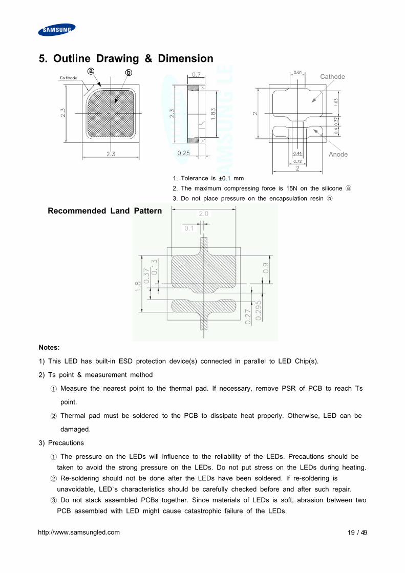
5. Outline Drawing & Dimension
Recommended Land Pattern
Notes:
1) This LED has built-in ESD protection device(s) connected in parallel to LED Chip(s).
2) Ts point & measurement method
① Measure the nearest point to the thermal pad. If necessary, remove PSR of PCB to reach Ts
point.
② Thermal pad must be soldered to the PCB to dissipate heat properly. Otherwise, LED can be
damaged.
3) Precautions
① The pressure on the LEDs will influence to the reliability of the LEDs. Precautions should be
taken to avoid the strong pressure on the LEDs. Do not put stress on the LEDs during heating.
② Re-soldering should not be done after the LEDs have been soldered. If re-soldering is
unavoidable, LED`s characteristics should be carefully checked before and after such repair.
③ Do not stack assembled PCBs together. Since materials of LEDs is soft, abrasion between two
PCB assembled with LED might cause catastrophic failure of the LEDs.
Anode
Cathode
1. Tolerance is ±0.1 mm
2. The maximum compressing force is 15N on the silicone
3. Do not place pressure on the encapsulation resin
2.0
0.1
http://www.samsungled.com 20 / 49
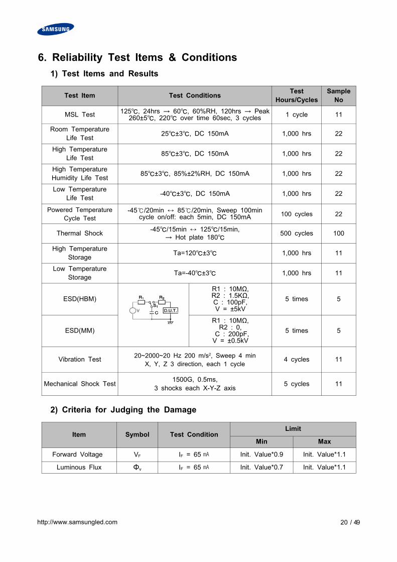
6. Reliability Test Items & Conditions
1) Test Items and Results
Test Item Test ConditionsTest
Hours/Cycles
Sample
No
MSL Test125, 24hrs → 60, 60%RH, 120hrs → Peak260±5, 220 over time 60sec, 3 cycles
1 cycle 11
Room Temperature
Life Test25±3, DC 150mA 1,000 hrs 22
High Temperature
Life Test85±3, DC 150mA 1,000 hrs 22
High Temperature
Humidity Life Test85±3, 85%±2%RH, DC 150mA 1,000 hrs 22
Low Temperature
Life Test-40±3, DC 150mA 1,000 hrs 22
Powered Temperature
Cycle Test
-45/20min ↔ 85/20min, Sweep 100mincycle on/off: each 5min, DC 150mA 100 cycles 22
Thermal Shock-45/15min ↔ 125/15min,
→ Hot plate 180500 cycles 100
High Temperature
StorageTa=120±3 1,000 hrs 11
Low Temperature
StorageTa=-40±3 1,000 hrs 11
ESD(HBM)
R1 : 10MΩ,R2 : 1.5KΩ,C : 100pF,V = ±5kV
5 times 5
ESD(MM)
R1 : 10MΩ,R2 : 0,C : 200pF,V = ±0.5kV
5 times 5
Vibration Test20~2000~20 Hz 200 m/s2, Sweep 4 min
X, Y, Z 3 direction, each 1 cycle4 cycles 11
Mechanical Shock Test1500G, 0.5ms,
3 shocks each X-Y-Z axis5 cycles 11
2) Criteria for Judging the Damage
Item Symbol Test ConditionLimit
Min Max
Forward Voltage VF IF = 65 Init. Value*0.9 Init. Value*1.1
Luminous Flux Φv IF = 65 Init. Value*0.7 Init. Value*1.1
http://www.samsungled.com 21 / 49
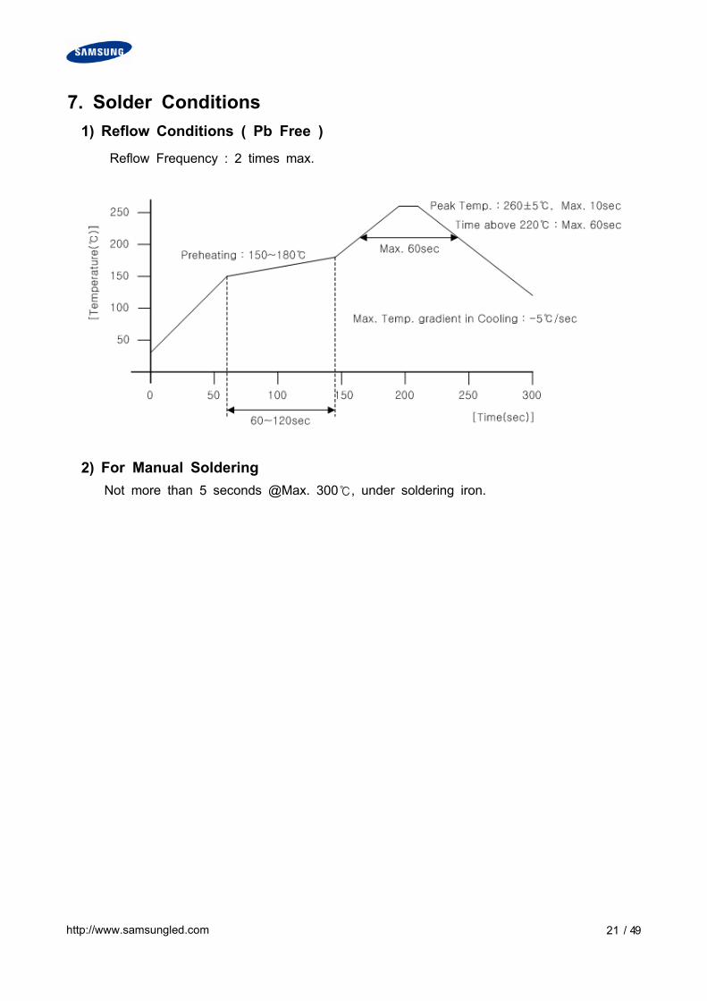
7. Solder Conditions
1) Reflow Conditions ( Pb Free )
Reflow Frequency : 2 times max.
2) For Manual Soldering
Not more than 5 seconds @Max. 300, under soldering iron.

http://www.samsungled.com 22 / 49
8. Tape & Reel
(1) Quantity : The quantity/reel to be 4,000 pcs.
(2) Cumulative Tolerance : Cumulative tolerance/10 pitches to be ±0.2
(3) Adhesion Strength of Cover Tape : Adhesion strength to be 0.1-0.7 N when the
cover tape is turned off from the carrier tape at 10 angle to be the carrier tape.
(4) Packaging : P/N, Manufacturing data code no. and quantity to be indicated on a
damp proof package.
More than 40
Unloaded tape
Mounted with
Flash LED
Leading part more than
(200~400)
More than (100~200)
Unloaded tape
EndStart
http://www.samsungled.com 23 / 49
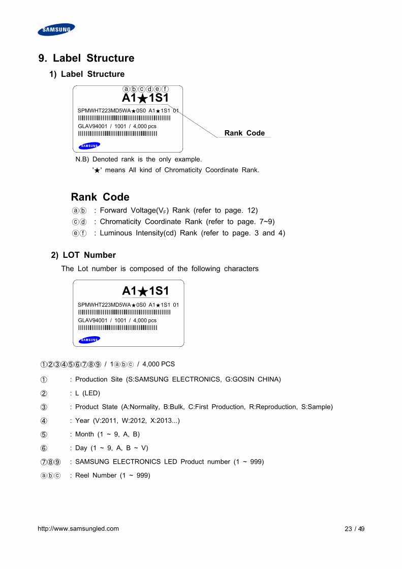
9. Label Structure
1) Label Structure
N.B) Denoted rank is the only example.
'' means All kind of Chromaticity Coordinate Rank.
Rank Code
: Forward Voltage(VF) Rank (refer to page. 12)
: Chromaticity Coordinate Rank (refer to page. 7~9)
: Luminous Intensity(cd) Rank (refer to page. 3 and 4)
2) LOT Number
The Lot number is composed of the following characters
①②③④⑤⑥⑦⑧⑨ / 1 / 4,000 PCS
① : Production Site (S:SAMSUNG ELECTRONICS, G:GOSIN CHINA)
② : L (LED)
③ : Product State (A:Normality, B:Bulk, C:First Production, R:Reproduction, S:Sample)
④ : Year (V:2011, W:2012, X:2013...)
⑤ : Month (1 ~ 9, A, B)
⑥ : Day (1 ~ 9, A, B ~ V)
⑦⑧⑨ : SAMSUNG ELECTRONICS LED Product number (1 ~ 999)
: Reel Number (1 ~ 999)
SPMWHT223MD5WA0S0 A11S1 01
IIIIIIIIIIIIIIIIIIIIIIIIIIIIIIIIIIIIIIIIIIIIIIIIIGLAV94001 / 1001 / 4,000 pcs
IIIIIIIIIIIIIIIIIIIIIIIIIIIIIIIIIIIIIIIIII
Rank Code
A11S1
SPMWHT223MD5WA0S0 A11S1 01
IIIIIIIIIIIIIIIIIIIIIIIIIIIIIIIIIIIIIIIIIIIIIIIIIGLAV94001 / 1001 / 4,000 pcs
IIIIIIIIIIIIIIIIIIIIIIIIIIIIIIIIIIIIIIIIII
A11S1
http://www.samsungled.com 24 / 49
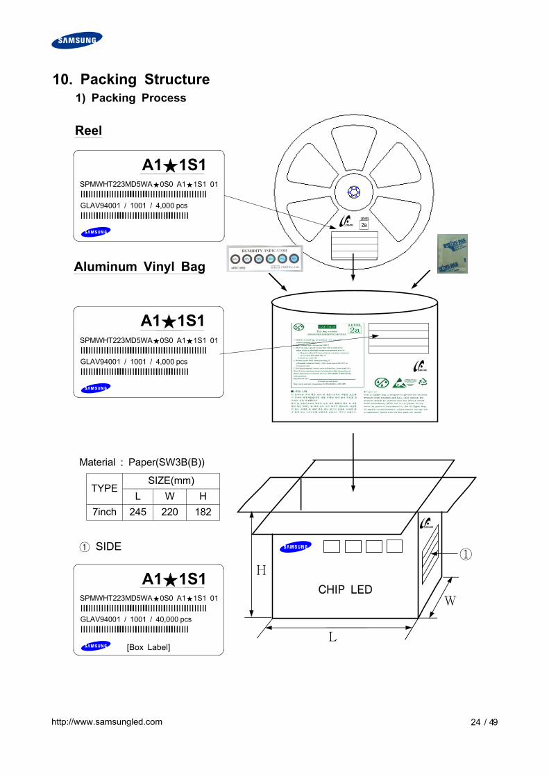
10. Packing Structure
1) Packing Process
Reel
Aluminum Vinyl Bag
LEVEL
2a
LEVEL
2a
[Box Label]
SPMWHT223MD5WA0S0 A11S1 01
IIIIIIIIIIIIIIIIIIIIIIIIIIIIIIIIIIIIIIIIIIIIIIIIIGLAV94001 / 1001 / 4,000 pcs
IIIIIIIIIIIIIIIIIIIIIIIIIIIIIIIIIIIIIIIIII
A11S1
SPMWHT223MD5WA0S0 A11S1 01
IIIIIIIIIIIIIIIIIIIIIIIIIIIIIIIIIIIIIIIIIIIIIIIIIGLAV94001 / 1001 / 4,000 pcs
IIIIIIIIIIIIIIIIIIIIIIIIIIIIIIIIIIIIIIIIII
A11S1
SPMWHT223MD5WA0S0 A11S1 01
IIIIIIIIIIIIIIIIIIIIIIIIIIIIIIIIIIIIIIIIIIIIIIIIIGLAV94001 / 1001 / 40,000 pcs
IIIIIIIIIIIIIIIIIIIIIIIIIIIIIIIIIIIIIIIIII
A11S1
① SIDE
Material : Paper(SW3B(B))
TYPESIZE(mm)
L W H
7inch 245 220 182
CHIP LED
①H
W
L
http://www.samsungled.com 25 / 49
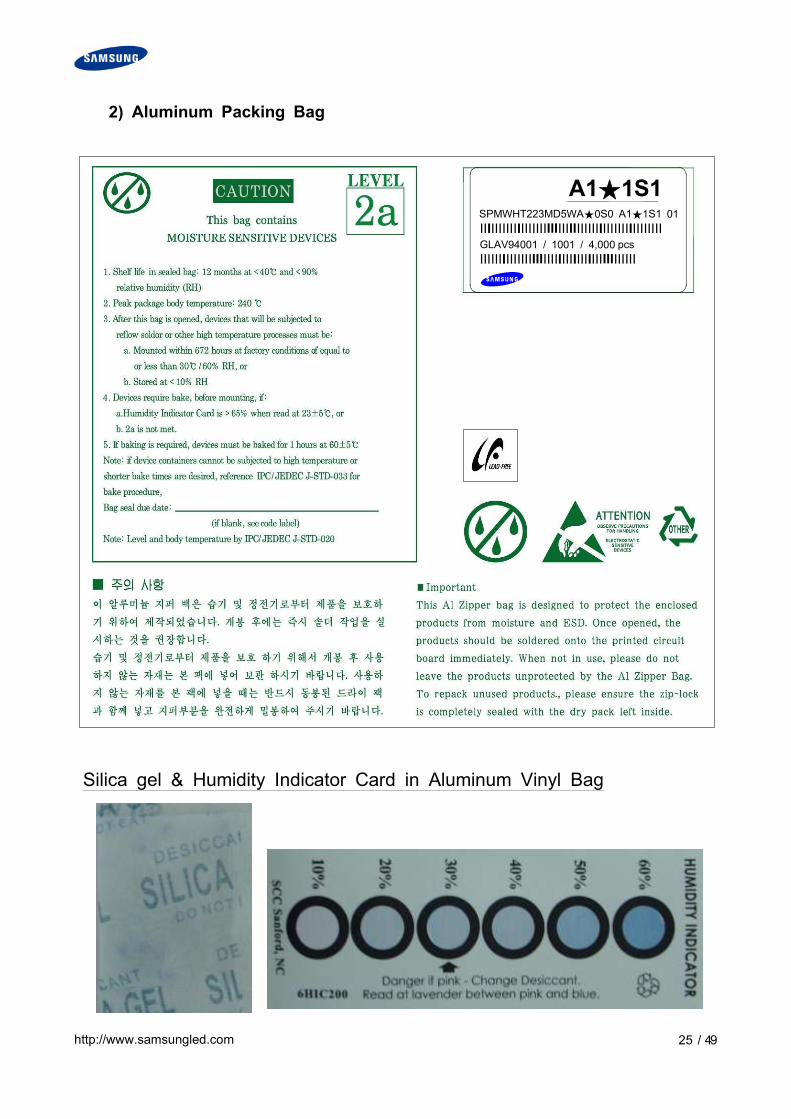
2) Aluminum Packing Bag
Silica gel & Humidity Indicator Card in Aluminum Vinyl Bag
SPMWHT223MD5WA0S0 A11S1 01
IIIIIIIIIIIIIIIIIIIIIIIIIIIIIIIIIIIIIIIIIIIIIIIIIGLAV94001 / 1001 / 4,000 pcs
IIIIIIIIIIIIIIIIIIIIIIIIIIIIIIIIIIIIIIIIII
A11S1
http://www.samsungled.com 26 / 49
11. Precaution for use
1) For over-current-proof function, customers are recommended to apply resistors to
prevent sudden change of the current caused by slight shift of the voltage.
과전류 방지를 위해 전압의 미세한 이동에 의해 야기되는 전류의 순간 변화를 방지하기
위해 저항 등의 설치를 권장함.
2) This device should not be used in any type of fluid such as water, oil, organic
solvent, etc. When washing is required, IPA is recommended to use.
제품은 물, 오일, 유기물과 같은 액체 타입에서의 사용은 제한되며,
세정이 필요할 시에는 IPA 사용을 권장함.
3) When the LEDs illuminate, operating current should be decided after considering the
ambient maximum temperature.
LED의 발광 시, 동작 전류는 주변 최고온도를 고려하여 결정되어야 함.
4) LEDs must be stored in a clean environment.
If the LEDs are to be stored for 3 months or more after being shipped from
Samsung Electronics, they should be packed by a sealed container with nitrogen gas
injected.(Shelf life of sealed bags: 12 months, temp. ~40, ~90%RH)
LED의 보관은 청정한 환경에서 보존되어져야 하며, 만약 삼성전자로부터 공급받는 후
3개월 또는 그 이상 보관이 필요하다면 질소 가스를 동봉한 보존용기에 보관되어야 함.
(보존 bag의 수명 : 12 개월, 보존 온도 ~40, 습도 ~90%RH)
5) After storage bag is open, device subjected to soldering, solder reflow, or other
high temperature processes must be:
보존 Bag이 개봉된 후에, 납땜이나 reflow등의 높은 온도에 노출되는 제품은 다음의
사항에 부합되어야 함.
a. Mounted within 672 hours(28 days) at an assembly line with a condition of no
more than 30/60%RH,
a. 제품은 30/60%RH보다 같거나 낮은 조립조건에서 672시간(28일)이내에 조립해야 함.
b. Stored at <10%RH.
b. 10% 이하의 상대습도에서 보관되어야 함.
6) Repack unused Products with anti-moisture packing, fold to close any opening and
then store in a dry place.
사용하지 않은 제품은 방습팩에 넣어 개봉 부위를 닫아서 다시 포장한 후,
건조한 장소에서 보관할 것을 권장함.
http://www.samsungled.com 27 / 49
7) Devices require baking before mounting, if humidity card reading is >60% at 23±5.
만약 습도표시카드의 수치가 23±5에서 60% 이상이라면, 제품 실장 전 baking해야 함.
8) Devices must be baked for 1 hour at 65±5, if baking is required.
만약 baking이 필요하다면, 제품은 65±5에서 1시간 정도 baking 되어야 함.
9) The LEDs are sensitive to the static electricity and surge. It is recommended to
use a wrist band or anti-electrostatic glove when handling the LEDs.
LED는 정전기 및 서지에 민감한 제품이므로, LED 제품을 다룰 시에는 정전기
방지장갑이나 손목밴드를 사용하기를 권장함.
If voltage exceeding the absolute maximum rating is applied to LEDs, it may cause
damage or even destruction to LED devices.
만약 절대 허용치를 초과하는 전압이 LED에 가해지면, LED 소자는 파괴되거나
손상될 수 있음.
Damaged LEDs may show some unusual characteristics such as increase in leak
current, lowered turn-on voltage, or abnormal lighting of LEDs at low current.
손상된 제품은 누설전류의 증가, Turn on 전압의 저하, 저 전류에서의 점등불량 등의
이상 거동을 보일 수 있음.
10) VOCs (volatile organic compounds) can be generated from adhesives, flux, hardener
or organic additives used in luminaires (fixtures). Transparent LED silicone
encapsulant is permeable to those chemicals and they may lead a discoloration of
encapsulant when they expose to heat or light.
VOCs(휘발성 유기 화합물)는 등기구에 사용되는 접착제, Flux, 경화제,
유기물 첨가제에서 발생하여 LED 실리콘 봉지제를 투과하고,
빛 또는 열에 노출되었을 때 변색이 발생 할 수 있음.
This phenomenon can cause a significant loss of light emitted(output) from the
luminaires(fixtures).
이러한 현상은 등기구로부터 나오는 빛의 중대한 손실을 줄 수 있음.
In order to prevent these problems, we recommend you to know the physical
properties of materials used in luminaires, They must be selected carefully.
이러한 문제 발생 방지를 위해서, 등기구에 사용되는 자재에 대한 물성을 알고
주의하여 선택 되어야함.
http://www.samsungled.com 28 / 49
11) Risk of Sulfurization (or Tarnishing)
The LED from Samsung Electronics uses a silver-plated lead frame and its surface
color may change to black(or dark colored) when it is exposed to sulfur (S), chlorine
(Cl) or other halogen compound
삼성전자의 LED는 Ag(은)을 도금한 리드프레임을 사용함. 이 리드프레임의 표면이
황(S), 염소(Cl), 또는 다른 할로겐 화합물들에 노출시 Ag(은)은 검정(또는 어두운색)으로
바뀔 수 있음.
Sulfurization of the lead frame may cause intensity degradation, change of
chromaticity coordinates and, in extreme cases. open circuit. It requires
caution.
리드 프레임의 황화(Sulfurization)는 광량 저하, 색좌표 변화 및 심한 경우 회로내의
LED 무등(Open) 불량을 일으킬 수도 있으니 주의가 필요함.
Due to possible sulfurization of lead frame, LED should not be used and stored
together with oxidizing substances made of materials in a following list,
: Rubber, Plain paper, lead solder cream and so on.
리드 프레임 황화(Sulfurization)의 근원이 될 수 있으니 LED는 아래의 목록으로
만들어진 산화성 물질들과 함께 저장, 사용이 불가함 : 고무, 일반 종이, 납땜 크림 등
http://www.samsungled.com 29 / 49
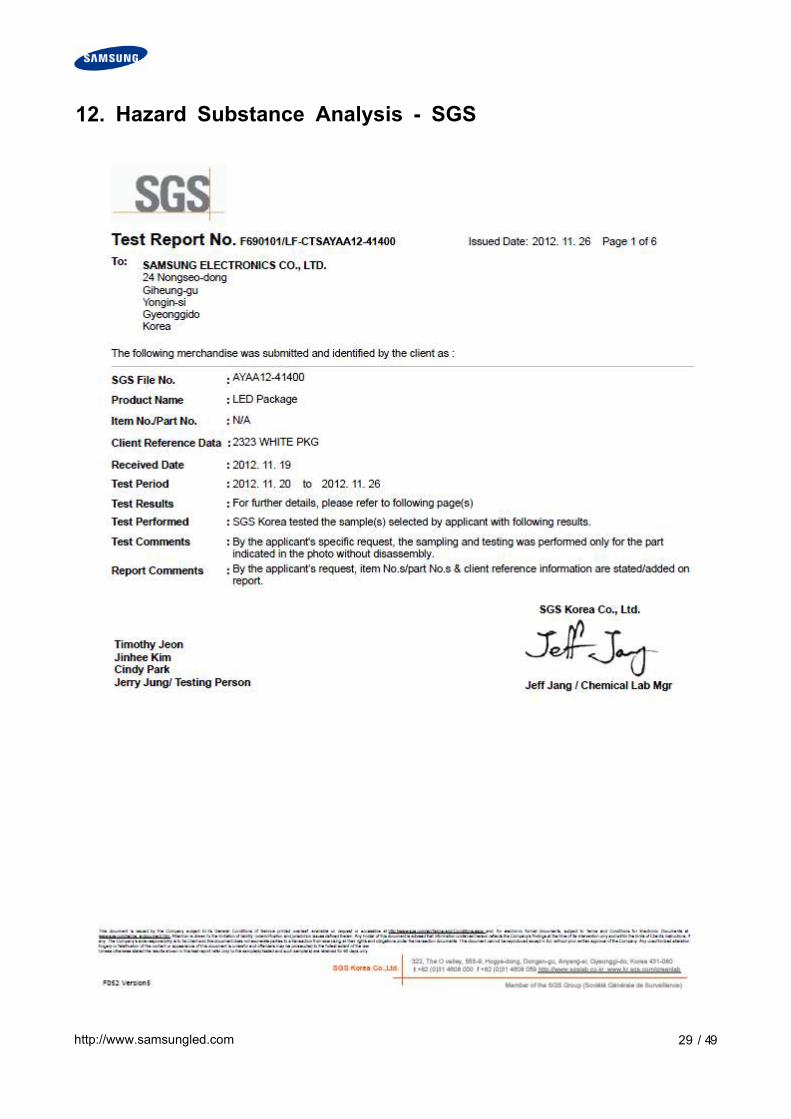
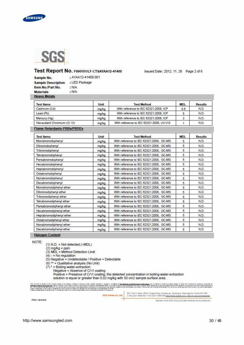
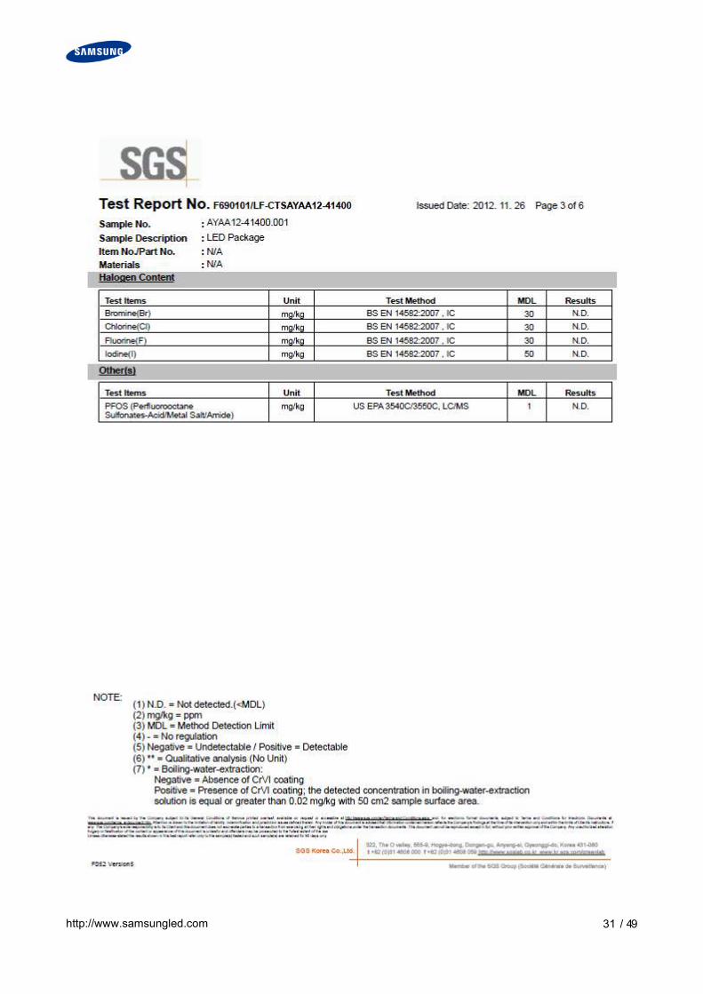
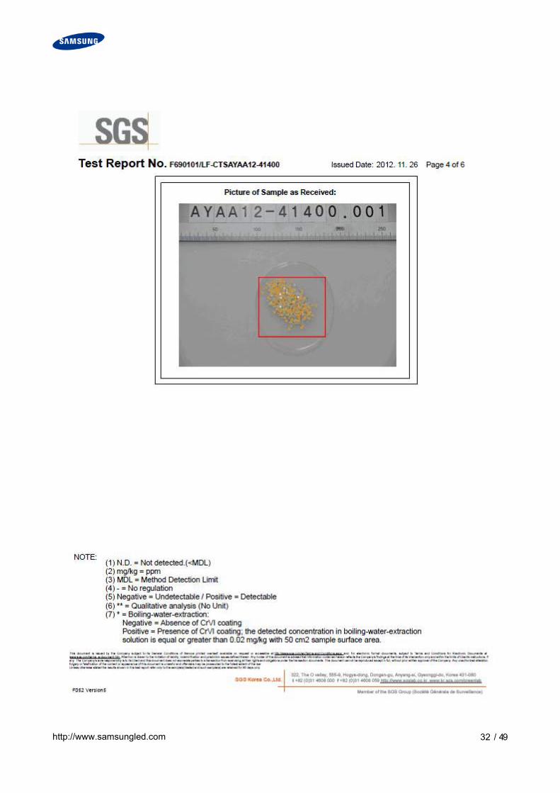
12. Hazard Substance Analysis - SGS
http://www.samsungled.com 30 / 49
http://www.samsungled.com 31 / 49
http://www.samsungled.com 32 / 49

http://www.samsungled.com 33 / 49
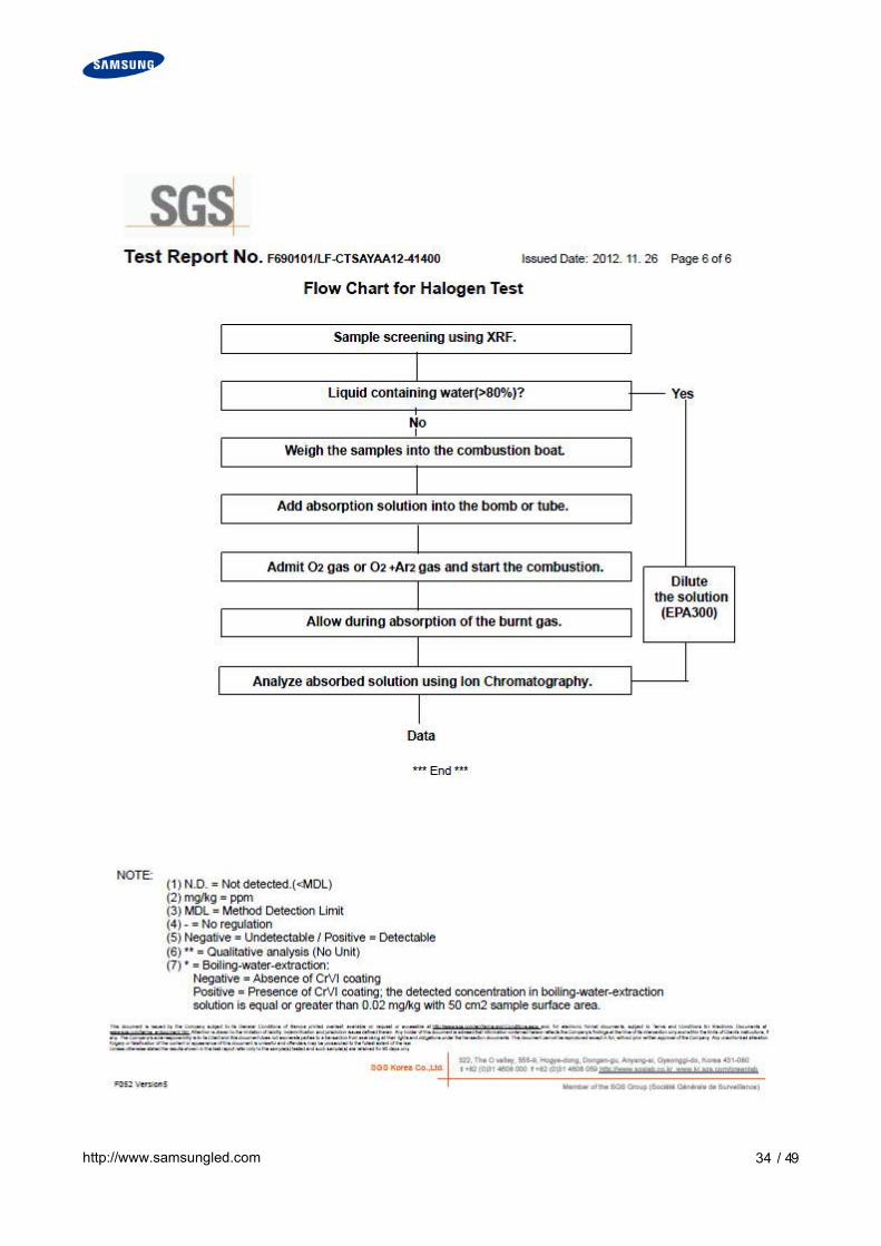
http://www.samsungled.com 34 / 49
http://www.samsungled.com 35 / 49
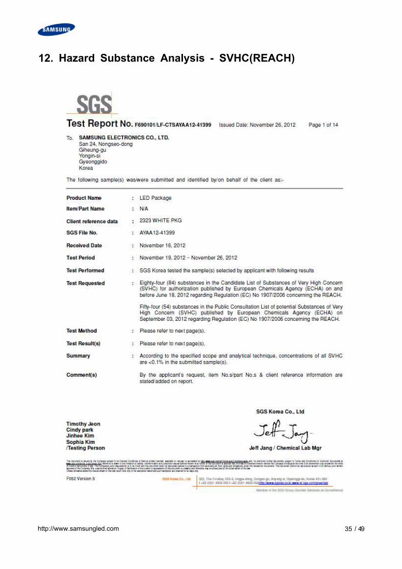
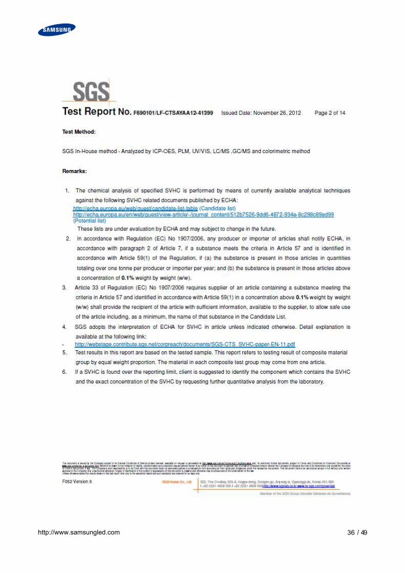
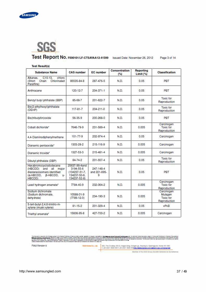
12. Hazard Substance Analysis - SVHC(REACH)
http://www.samsungled.com 36 / 49
http://www.samsungled.com 37 / 49
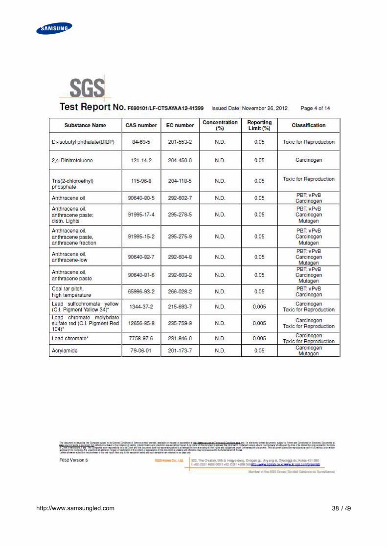
http://www.samsungled.com 38 / 49

http://www.samsungled.com 39 / 49
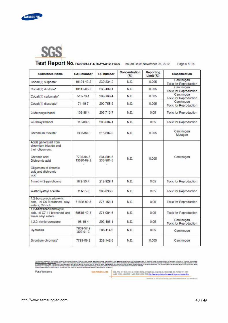
http://www.samsungled.com 40 / 49
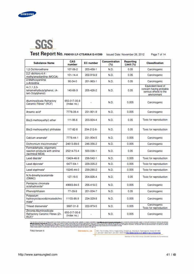
http://www.samsungled.com 41 / 49
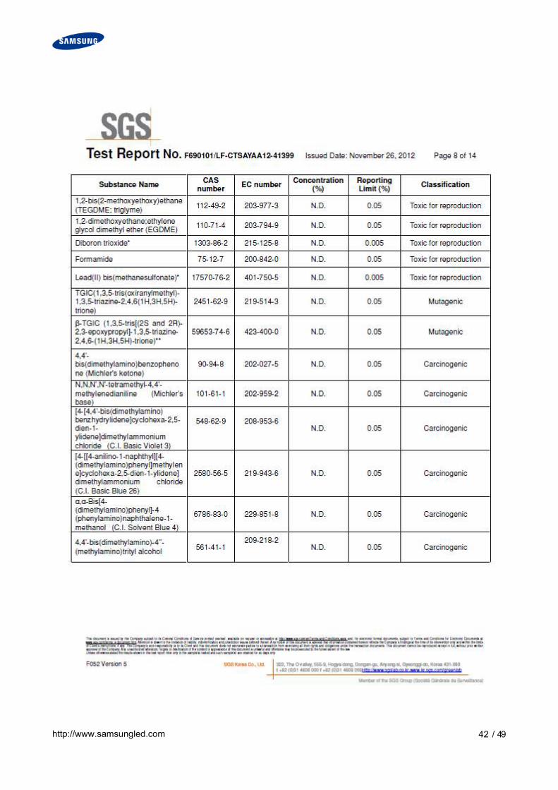
http://www.samsungled.com 42 / 49
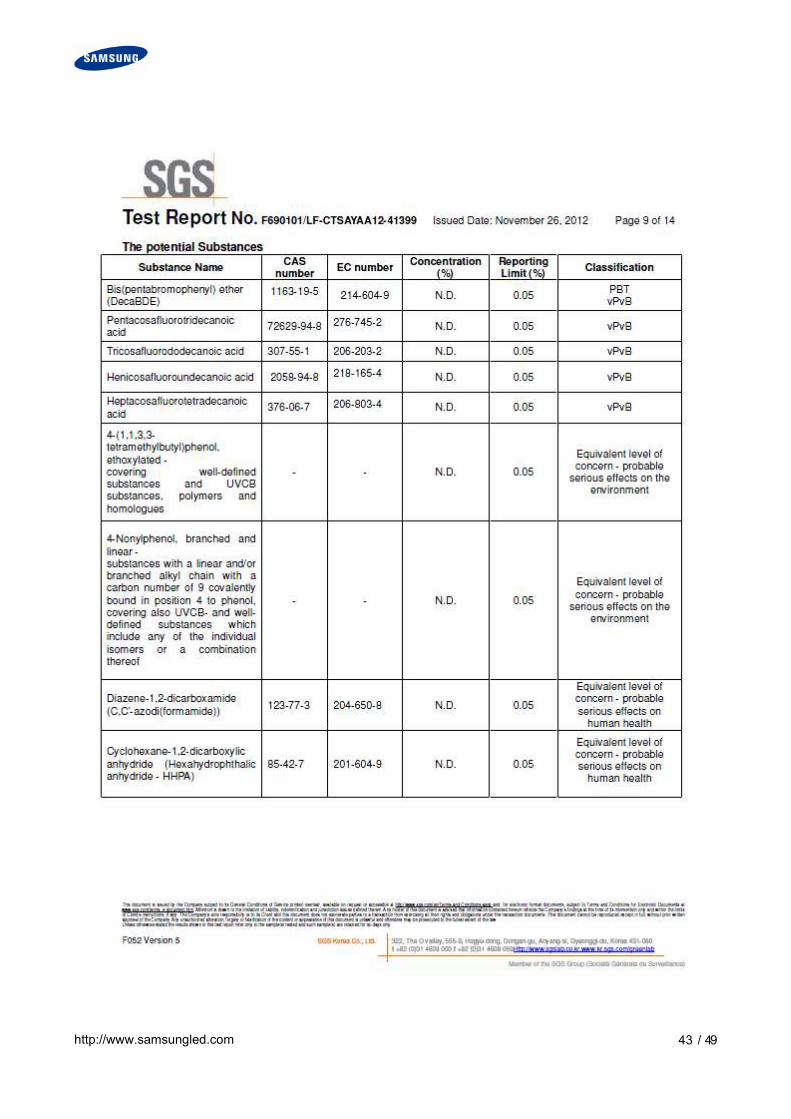
http://www.samsungled.com 43 / 49
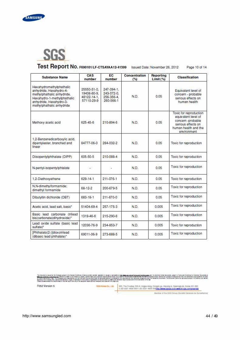
http://www.samsungled.com 44 / 49
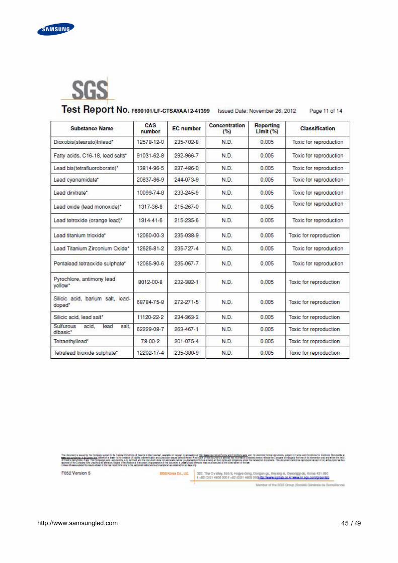
http://www.samsungled.com 45 / 49
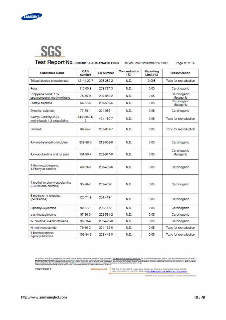
http://www.samsungled.com 46 / 49
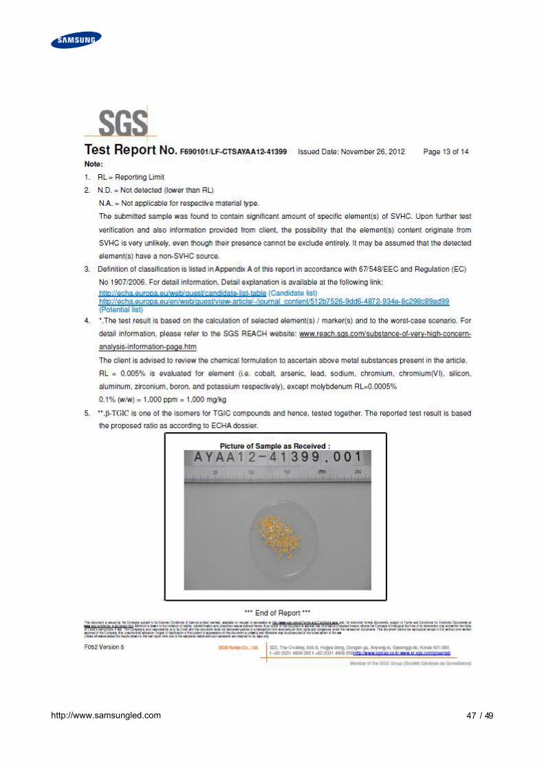
http://www.samsungled.com 47 / 49

http://www.samsungled.com 48 / 49
http://www.samsungled.com 49 / 49
Date N0 Revision HistoryWriter
Drawn Approved
2013.02.14 001 New version T.J KIM Y.T KIM
2013.04.08 002 6500K, 5700K, 5000K CIE 8분할 적용 T.J KIM Y.T KIM
Revision History