ljlwdo ,qwhjudwhg &lufxlwv ,, /hfwxuh...
TRANSCRIPT

EE213 L05 Wires.1 Pingqiang, ShanghaiTech, 2017
EE213Digital Integrated Circuits II
Lecture 05: Wires
ShanghaiTech UniversitySchool of Information Science and Technology
Prof. Pingqiang Zhou
http://sist.shanghaitech.edu.cn/faculty/zhoupq/Teaching/Spr17/Digital-IC-2.html

EE213 L05 Wires.2 Pingqiang, ShanghaiTech, 2017
Materials were partly taken from
EE141: Digital Integrated Circuits, Spring 2010. http://bwrcs.eecs.berkeley.edu/Classes/icdesign/ee141_s10/index.htm
Cha
pter 4
Cha
pter 5

EE213 L05 Wires.3 Pingqiang, ShanghaiTech, 2017
Metal Layer Stack
Intel 45 nm Stack
[Thompson02]
[Moon08]
Intel 90 nm Stack

EE213 L05 Wires.4 Pingqiang, ShanghaiTech, 2017
# of Wiring Layers
# of metal layers is steadily increasing due to:
• Increasing die size and device count: we need more wires and longer wires to connect everything.
• Rising need for a hierarchical wiring network; local wires with high density and global wires with low RC.
substrate
poly
M1
M2
M3
M4
M5
M6
Tins
H
WS
= 2.2 -cm
0.25 m wiring stack
Minimum Widths (Relative)
0.0
0.5
1.0
1.5
2.0
2.5
3.0
3.5
M5
M4
M3
M2
M1
Poly
Minimum Spacing (Relative)
0.0
0.5
1.0
1.5
2.0
2.5
3.0
3.5
4.0
M5
M4
M3
M2
M1
Poly

EE213 L05 Wires.5 Pingqiang, ShanghaiTech, 2017
Characteristics of Interconnects
10 100 1,000 10,000 100,000
Length (u)
No
of
net
s(L
og
Sca
le)
Pentium Pro (R)
Pentium(R) II
Pentium (MMX)
Pentium (R)
Pentium (R) II
Local Interconnect
Global Interconnect
SLocal = STechnology
SGlobal = SDie
So
urc
e:
Inte
l

EE213 L05 Wires.6 Pingqiang, ShanghaiTech, 2017
The Local Wire
transmitters receivers
schematics
physical

EE213 L05 Wires.7 Pingqiang, ShanghaiTech, 2017
Single-Ended Static Driver and Receiver
CL
VDD
VDD VDD
driver receiver
VDDL
VDDLIn
OutOut

EE213 L05 Wires.8 Pingqiang, ShanghaiTech, 2017
System Level Signal Interconnect
Ain Bin Cin Din
Wout Xout Yout Zout
TristateBusdrivers
Busreceivers
Bus
Classes of global interconnects System level signal interconnect
Global set and reset lines
System clock(s)
VDD and GND planes

EE213 L05 Wires.9 Pingqiang, ShanghaiTech, 2017
On-die Data Movement vs Compute
• Interconnect energy (per mm) reduces slower than compute
• On-die data movement energy will start to dominate
0
0.2
0.4
0.6
0.8
1
1.2
90 65 45 32 22 14 10 7Technology (nm)Source: Intel
On die IC energy/mm
Compute energy
6X
60%
[Intel, Borkar, 2015]

EE213 L05 Wires.10 Pingqiang, ShanghaiTech, 2017
Interconnect vs Switch Energy
0
0.25
0.5
0.75
1
100
1000
10000
0 5 10 15 20 25
pJ/BitDelay (ps)
On-die interconnect length (mm)
Switch delay
Switch energy
Switch energyWith scaling
Repeated wire delayWire energy
[Intel, Borkar, 2015]
EE213 L05 Wires.11 Pingqiang, ShanghaiTech, 2017
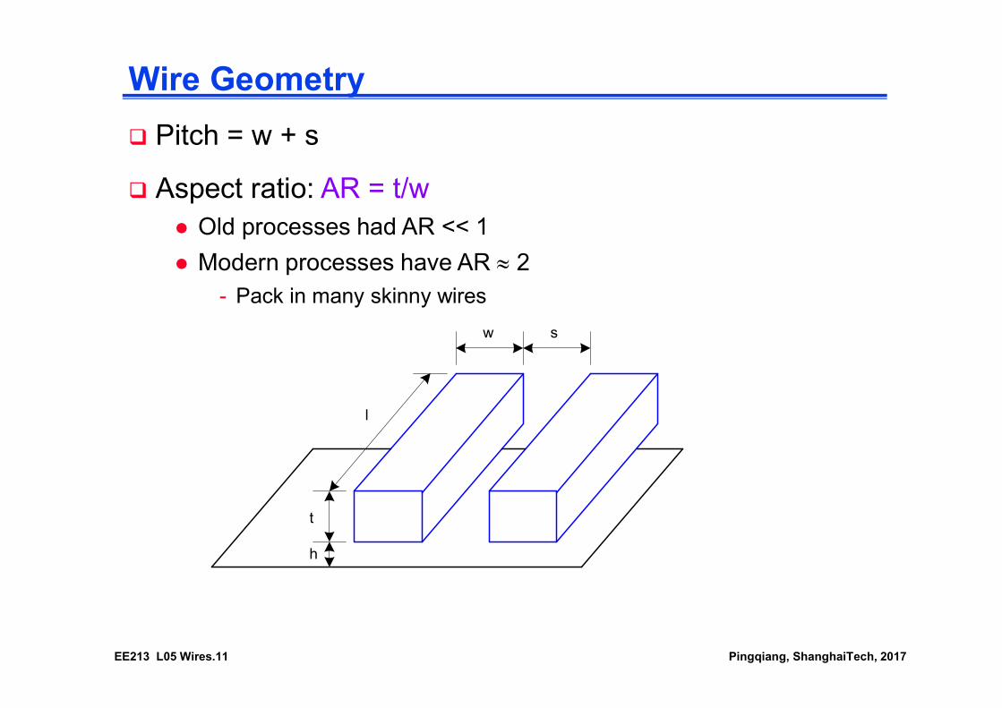
Wire Geometry
Pitch = w + s
Aspect ratio: AR = t/w Old processes had AR << 1
Modern processes have AR 2- Pack in many skinny wires
l
w s
t
h

EE213 L05 Wires.12 Pingqiang, ShanghaiTech, 2017
Example of Wire Geometry

EE213 L05 Wires.13 Pingqiang, ShanghaiTech, 2017
Parasitic Modeling of Interconnect
Two inverters communicating over a long interconnect Interconnect has potential difference with surroundings
- Electric field E, modeled as capacitor
Current flows through the interconnect loop- Magnetic flux density B linked by the loop, modeled as inductor

EE213 L05 Wires.14 Pingqiang, ShanghaiTech, 2017
Interconnect Modeling
Current in a wire is analogous to current in a pipe
Resistance: narrow size impedes flow
Capacitance: trough under the leaky pipe must fill first
Inductance: paddle wheel inertia opposes changes in flow rate
- Negligible for most wires
l
w s
t
h

EE213 L05 Wires.15 Pingqiang, ShanghaiTech, 2017
Wire Models
All-inclusive Model
l
w s
t
h
Intel 45 nm Stack
[Moon08]

EE213 L05 Wires.16 Pingqiang, ShanghaiTech, 2017
INTERCONNECT

EE213 L05 Wires.17 Pingqiang, ShanghaiTech, 2017
Sources of Resistance
MOS structure resistance - Ron
Source and drain resistance
Contact (via) resistance
Wiring resistance
Top view
Drain n+ Source n+
W
L
Poly Gate

EE213 L05 Wires.18 Pingqiang, ShanghaiTech, 2017
Wire Resistance
L
W
H
R = L
H W
Sheet Resistance R
L
A=
Material (-m)
Silver (Ag) 1.6 x 10⁻⁸
Copper (Cu) 1.7 x 10⁻⁸
Gold (Au) 2.2 x 10⁻⁸
Aluminum (Al) 2.7 x 10⁻⁸
Tungsten (W) 5.5 x 10⁻⁸
Material Sheet Res. (/)
n, p well diffusion 1000 to 1500
n+, p+ diffusion 50 to 150
n+, p+ diffusion w/ silicide 3 to 5
polysilicon 150 to 200
polysilicon w/ silicide 4 to 5
Aluminum 0.05 to 0.1
EE213 L05 Wires.19 Pingqiang, ShanghaiTech, 201719
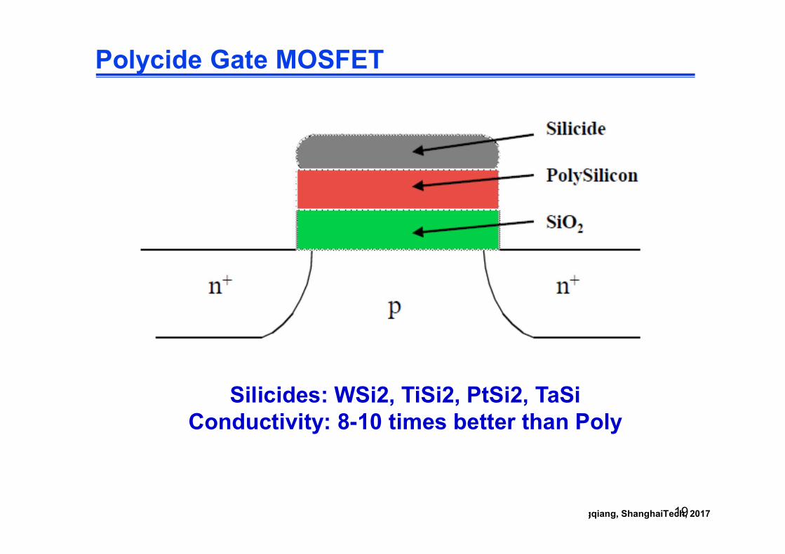
Polycide Gate MOSFET
Silicides: WSi2, TiSi2, PtSi2, TaSiConductivity: 8-10 times better than Poly

EE213 L05 Wires.20 Pingqiang, ShanghaiTech, 2017
Modern Interconnect

EE213 L05 Wires.21 Pingqiang, ShanghaiTech, 2017
Contacts Resistance Typical contact resistances, RC,
5 to 20 for metal or poly to n+, p+ diffusion, and metal to poly
2 to 20 for metal to metal contacts
More pronounced with scaling since contact openings are smaller
Vias add extra resistance to a wire keep signals wires on a single layer if possible
avoid excess contacts
using multiple vias to make the contact

EE213 L05 Wires.22 Pingqiang, ShanghaiTech, 2017
Skin Effect At high frequency, currents tend to flow on the surface of a conductor
with the current density falling off exponentially with depth into the wire
H
W
where f is frequency = 4 x 10⁻⁷ H/m
so the overall cross section is ~ 2(W+H)
= 2.6 mfor Al at 1 GHz
The onset of skin effect is at fs - where the skin depth is equal to half the largest dimension of the wire.
fs = 4 / ( (max(W,H))2)
An issue for high frequency, wide (tall) wires (i.e., clocks!)

EE213 L05 Wires.23 Pingqiang, ShanghaiTech, 2017
Skin Effect for Different W’s
A 30% increase in resistance is observe for 20 m Al wires at 1 GHz (versus only a 1% increase for 1 m wires)
0.1
1
10
100
1000
Frequency (Hz)
% In
cre
ase
in R
esi
stan
ce
W = 1 um
W = 10 um
W = 20 um
1E8 1E9 1E10
for H = .70 um

EE213 L05 Wires.24 Pingqiang, ShanghaiTech, 2017
Impact of Resistance
We have already learned how to drive RC interconnect
Impact of resistance is commonly seen in power supply distribution:
IR drop
Voltage variations
Power supply is distributed to minimize the IR drop and the change in current due to switching of gates
transmitters receivers

EE213 L05 Wires.25 Pingqiang, ShanghaiTech, 2017
Deliver power from board to each gate on chip.
[Te
xas
ele
ctric
ity a
llia
nce]
Power delivery system [Eby Friedman] Electricity grid
Gates on chip
Power supply pin
Metal wire
On-chip power grid (power density >10W/cm2)
Power Supply System

EE213 L05 Wires.26 Pingqiang, ShanghaiTech, 2017

EE213 L05 Wires.27 Pingqiang, ShanghaiTech, 2017
Del
ay
(ns)
2.4 2.6 2.8 3.0 3.2 VDD
0.2
0
.3
0.4
0
.5
Vdd (V)
Cell
Rns
Idd
Iss
Vdd Pin
Vss Pin
Lpd Rpd
Cpd
Lps
Cps
Rps
Rnd
Vdd
Vss
Vdd Net
Vss Net
Cnd
Cns
Vss t
V
Vdd
Power Supply Noise

EE213 L05 Wires.28 Pingqiang, ShanghaiTech, 2017
Average(17 ckts)
w/ noise:1.15
w/o noise:1.00
0
0.2
0.4
0.6
0.8
1
1.2
1.4
C5315 C6288 C7552 s13207 s15850 s38417 s38584 s35932
w/ supply noise w/o supply noise
Normalized circuit delay
Results are based on HSPICE (0.55um, 3.3V technology)
max. supply noise on critical path (V)0.53 0.60 0.59 0.55 0.53 0.62 0.60 0.58
Delay W/ and W/O Power Supply Noise
Source: Cheng, UCSB

EE213 L05 Wires.29 Pingqiang, ShanghaiTech, 2017
Average(17 ckts)
w/ noise:1.33w/o noise:1.00
0
0.2
0.4
0.6
0.8
1
1.2
1.4
1.6
C5315 C6288 C7552 s13207 s15850 s38417 s38584 s35932
w/ supply noise w/o supply noise
Normalized circuit delay
Results are based on HSPICE (0.25um, 2.5V technology)
max. supply noise on critical path (V)0.42 0.42 0.47 0.24 0.31 0.43 0.35 0.34
Delay W/ and W/O Power Supply Noise
Source: Cheng, UCSB

EE213 L05 Wires.30 Pingqiang, ShanghaiTech, 2017
Power and Ground Distribution
GND
VDD
Logic
GND
VDD
Logic
GND
VDD
(a) Finger-shaped network (b) Network with multiple supply pins

EE213 L05 Wires.31 Pingqiang, ShanghaiTech, 2017
Resistance and the Power Distribution Problem
Source: Cadence
• Requires fast and accurate peak current prediction• Heavily influenced by packaging technology
Before After

EE213 L05 Wires.32 Pingqiang, ShanghaiTech, 2017
INTERCONNECT

EE213 L05 Wires.33 Pingqiang, ShanghaiTech, 2017
Capacitance of Wire Interconnect
Fan-Out
Simplified Model

EE213 L05 Wires.34 Pingqiang, ShanghaiTech, 2017
Wire Capacitance: Parallel Plate
WLt
Cdi
dipp

EE213 L05 Wires.35 Pingqiang, ShanghaiTech, 2017
Wire Capacitance: Fringe Capacitance
Cwire Cpp +Cfringe ditdiWL+ 2di
log(tdi / H )L

EE213 L05 Wires.36 Pingqiang, ShanghaiTech, 2017
Fringing vs. Parallel Plate
(from [Bakoglu89])
2dilog(tdi /H )
L
ditdiWL

EE213 L05 Wires.37 Pingqiang, ShanghaiTech, 2017
Interwire Capacitance
interwire
fringe
W W
W
H
H
H
tdi
tdi
tdi
Cwire = Cpp + Cfringe + Cinterwire
= (di/tdi)WL + (2di)L/log(tdi/H) + (di/tdi)HL
pppp

EE213 L05 Wires.38 Pingqiang, ShanghaiTech, 2017
Wiring Capacitances
Field Active Poly Al1 Al2 Al3 Al4
Poly 88
54
Al1 30 41 57
40 47 54
Al2 13 15 17 36
25 27 29 45
Al3 8.9 9.4 10 15 41
18 19 20 27 49
Al4 6.5 6.8 7 8.9 15 35
14 15 15 18 27 45
Al5 5.2 5.4 5.4 6.6 9.1 14 38
12 12 12 14 19 27 52
fringe in aF/m
par. plate in aF/m2
Poly Al1 Al2 Al3 Al4 Al5
Interwire Cap 40 95 85 85 85 115
per unit wire length in aF/m for minimally-spaced wires

EE213 L05 Wires.39 Pingqiang, ShanghaiTech, 2017
Impact of Interwire Capacitance
From: Bakoglu89
Ctotal = Cinterwire + Cground
+ Cparallel-plate
At smaller feature size, the interwire cap.
dominates!

EE213 L05 Wires.40 Pingqiang, ShanghaiTech, 2017
Crosstalk
A capacitor does not like to change its voltage instantaneously.
A wire has high capacitance to its neighbor. When the neighbor switches from 1-> 0 or 0->1, the wire tends
to switch too.
Called capacitive coupling or crosstalk.
Crosstalk effects Noise on non-switching wires
Increased delay on switching wires
A BCadjCgnd Cgnd

EE213 L05 Wires.41 Pingqiang, ShanghaiTech, 2017
Crosstalk Delay
Effective Cadj depends on behavior of neighbors
A BCadjCgnd Cgnd
B DV Ceff(A) MCF
Constant VDD Cgnd + Cadj 1
Switching with A 0 Cgnd 0
Switching opposite A 2VDD Cgnd + 2 Cadj 2
R. Ho, K. W. Mai and M. A. Horowitz, "The future of wires," in Proceedings of the IEEE, vol. 89, no. 4, pp. 490-504, Apr 2001.
Cc
Delay and power increase
Miller effect

EE213 L05 Wires.42 Pingqiang, ShanghaiTech, 2017
Crosstalk Noise
Crosstalk causes noise on nonswitching wires
If victim is floating: model as capacitive voltage divider
A BCadjCgnd Cgnd
Cadj
Cgnd-v
Aggressor
Victim
DVaggressor
DVvictim
adj
gnd-v adaggresvictim o
js r
CV
C CV D
+D

EE213 L05 Wires.43 Pingqiang, ShanghaiTech, 2017
Driven Victims
Usually victim is driven by a gate that fights noise Noise depends on relative resistances
If sizes are same, Raggressor = 2-4 x Rvictim
A BCadjCgnd Cgnd
R. Ho, K. W. Mai and M. A. Horowitz, "The future of wires," in Proceedings of the IEEE, vol. 89, no. 4, pp. 490-504, Apr 2001.
Cadj
Cgnd-v
Aggressor
Victim
DVaggressor
DVvictim
Raggressor
Rvictim
Cgnd-a
DVvictim Cadj
Cgnd-v +Cadj
1
1+ kDVaggressor
aggressor gnd-aggresso a adj
gndvict -im victim j
r
v ad
C C
CR
Rk
C +
+

EE213 L05 Wires.44 Pingqiang, ShanghaiTech, 2017
Coupling Waveforms
Simulated coupling for Cadj = Cgnd
Aggressor (driven by a unit inverter)
Victim (undriven): 50%
Victim (half size driver): 16%
Victim (equal size driver): 8%
Victim (double size driver): 4%
t (ps)
0 200 400 600 800 1000 1200 1400 1800 2000
0
0.3
0.6
0.9
1.2
1.5
1.8
DVvictim
Cadj
Cgnd-v
Aggressor
Victim
DVaggressor
DVvictim
Raggressor
Rvictim
Cgnd-a
DVvictim Cadj
Cgnd-v +Cadj
1
1+ kDVaggressor
aggressor gnd-aggresso a adj
gndvict -im victim j
r
v ad
C C
CR
Rk
C +
+

EE213 L05 Wires.45 Pingqiang, ShanghaiTech, 2017
Noise Implications
So what if we have noise? If the noise is less than the noise margin, nothing happens
Static CMOS logic will eventually settle to correct output even if disturbed by large noise spikes
- But glitches cause extra delay
- Also cause extra power from false transitions
Dynamic logic never recovers from glitches
Memories and other sensitive circuits also can produce the wrong answer
Crosstalk Reduction Techniques?

EE213 L05 Wires.46 Pingqiang, ShanghaiTech, 2017
Wire Spacing
Spacing
Extra space

EE213 L05 Wires.47 Pingqiang, ShanghaiTech, 2017
Wire Spacing

EE213 L05 Wires.48 Pingqiang, ShanghaiTech, 2017
Power Supply Shielding
Add VDD and VSS “shields” between signal wires
Power supply lines isolate the wires and eliminate crosstalk effects caused by adjacent wire transitions
GND
GND
Shieldingwire
Substrate(GND)
Shieldinglayer
VDD

EE213 L05 Wires.49 Pingqiang, ShanghaiTech, 2017
Buffer Insertion
Buffer insertion is a traditional timing technique that can aid in noise tolerance as well Reduces the parallel length of interconnects and redistributes the
capacitive coupling between two newly created wires