linking the operating parameters of chemical vapor
TRANSCRIPT

RESEARCH
ARTIC
LE
Copyright © 2011 American Scientific PublishersAll rights reservedPrinted in the United States of America
Journal ofNanoscience and Nanotechnology
Vol. 11, 8132–8137, 2011
Linking the Operating Parameters of Chemical VaporDeposition Reactors with Film Conformality and Surface
Nano-Morphology
Nikolaos Cheimarios1, Sokratis Garnelis1, George Kokkoris2�∗, and Andreas G. Boudouvis11School of Chemical Engineering, National Technical University of Athens, Athens, GR-15780, Greece
2Institute of Microelectronics, NCSR “Demokritos,” Athens GR-15310, Greece
A multiscale modeling framework is used to couple the co-existing scales, i.e., macro-, micro- andnano-scale, in chemical vapor deposition (CVD) processes. The framework consists of a reactorscale model (RSM) for the description of the transport phenomena in the bulk phase (macro-scale)of a CVD reactor and two models for the micro- and nano-scale: (a) A feature scale model (FSM)describing the deposition of a film inside features on a predefined micro-topography on the waferand (b) a nano-morphology model (NMM) describing the surface morphology evolution during thinfilm deposition on an initially flat surface. The FSM is deterministic and consists of three sub-models:A ballistic model for the species’ transport inside features, a surface chemistry model, and a profileevolution algorithm based on the level set method. The NMM is stochastic and is based on thekinetic Monte Carlo method. The coupling of RSM with FSM is performed through a correction ofthe species consumption on the wafer. The linking of RSM with NMM is performed through “feeding”of the deposition rate calculated by RSM to the NMM. The case study is CVD of Silicon (Si) fromSilane. The effect of the reactor’s operating parameters on the Si film conformality inside trenches isinvestigated by the coupling of RSM with FSM. The formation of dimmers on an initially flat Si (001)surface as well as the periodic change of the surface nano-morphology is predicted.
Keywords: Multiscale Modeling, Silicon Deposition, Computational Fluid Dynamics, FeatureScale Model, Kinetic Monte Carlo, Nano-Morphology.
1. INTRODUCTION
The produced films via chemical vapor deposition (CVD)are utilized to a wide range of applications; from semi-conductor and micro-sensor devices to micro- and nano-electromechanical systems. Nowadays, the size of thesedevices shrinks to lower scales and the specifications of thefilms (thickness, conformality, surface morphology) referto properties in micro- or nano-scale. Thus, the single scaleconventional CVD modeling methods are not adequate.More advanced, multiscale modeling, methods are neededfor studying the phenomena in the co-existing (multiplelength) scales,1 in e.g., the filling of a micro-trench or thenano-morphology developing on a film’s surface duringdeposition.Generally, the co-existing length scales in a CVD pro-
cess are the macro- or reactor scale, micro- or fea-ture scale, and nano- or surface morphology scale. The
∗Author to whom correspondence should be addressed.
description of each scale requires a model: The reactorscale model (RSM) is used for the description of the trans-port phenomena in the bulk phase of the CVD reactor,the feature scale model (FSM) is used to describe the filmdeposition inside the features (e.g., trenches) and the nano-morphology model (NMM) is used to trail the surface mor-phology of the deposited film. The effect of the operationalparameters of a CVD reactor on the film profile evolu-tion inside a trench on the wafer or on the film surfacenano-morphology evolution can be predicted by linkingor coupling of RSM with FSM or NMM. The linking ofmodels refers to their sequential use, while the couplingincorporates a two-way interaction of the models.Several approaches to couple2–3 or link4–5 RSM with
FSM have been reported in the literature. The differ-ences in these approaches refer to the type of FSM used(deterministic or stochastic), to the application or not of atwo-way interaction, and the system studied. Concerningmultiscale modeling where the RSM is linked or coupledwith NMM interesting results on the interaction of the two
8132 J. Nanosci. Nanotechnol. 2011, Vol. 11, No. 9 1533-4880/2011/11/8132/006 doi:10.1166/jnn.2011.5076

RESEARCH
ARTIC
LE
Cheimarios et al. Linking the Operating Parameters of CVD Reactors with Film Conformality and Surface Nano-Morphology
scales can be found in Ref. [6] and in particular for Silicon(Si) in Ref. [7].In the present work, a multiscale modeling framework
including all models (scales) is presented. The aim is tolink the operating parameters of the CVD reactor with(a) film conformality inside trenches on the wafer and (b)surface nano-morphology of film deposited on an initiallyflat surface (see Fig. 1). In particular, the effect of oper-ating pressure, mole fraction of the precursor at the inlet,and mixture’s inlet flow on the film conformality insidelong rectangular trenches is investigated by coupling ofRSM with FSM. Furthermore, the nano-morphology of thedeposited film is reported at various positions on the wafer
(a)
(c)
deposition rate
(b)
εk,j
Fig. 1. The schematic of coupling: (a) CVD reactor. (b) The ‘interface’between RSM and FSM. �, T , and �i for all species are calculated byRSM and fed to the micro-scale. The surface rate correction coefficient,�k, is calculated by FSM and is returned back to macro-scale. A is thesurface of macro-scale through which computational information is trans-ferred to the surface of the features, A. (c) The ‘interface’ between RSMand NMM. The deposition rate calculated by the RSM is fed to theNMM.
by linking the computations of RSM with NMM. The casestudy for both implementations is CVD of Si from Silane(SiH4�.
2. MULTISCALE COMPUTATIONALFRAMEWORK
2.1. Reactor Scale Model (RSM)
The RSM describes the transport phenomena in the macro-scale of the CVD reactor. The governing equations arethe continuity, the momentum, the energy and the speciestransport equations3�8 which are solved numerically atsteady state to predict the velocity, pressure, temperatureand species distributions inside the bulk phase of the CVDreactor (see Fig. 1(a)). The CFD code Ansys 12/Fluent9 isused for the numerical solution of the aforementioned setof equations.
2.2. Feature Scale Model (FSM)
The FSM results from coupling a continuum ballisticmodel for the calculation of the local fluxes inside features,a surface model and a profile evolution algorithm. Theballistic model10�11 is used for the calculation of species’local fluxes inside the features (trenches or holes) at highKnudsen number conditions. It links the fluxes of thespecies at the wafer with the local fluxes inside the fea-tures. The surface model describes the surface processesand quantifies the effect of species’ fluxes on the localdeposition. The profile evolution algorithm of the growingfilm inside the features (moving boundary) uses the levelset method. Details for the implementation of the level setmethod to profile evolution problems in etching/depositioncan be found in Refs. [3, 12].
2.3. Nano-Morphology Model (NMM)
The NMM is based on the kinetic Monte Carlo method.The various portions of the wafer, at which the NMMis applied, are described as simple cubic lattices. Thedeveloped code supports the realization of three events:adsorption, desorption and diffusion of the adatoms on thesurface.13 Periodic boundary conditions are applied in thex–y plane to avoid edge effects.The probability of every event is related to its rate. The
adsorption rate is calculated as a collisional flux. Des-orption and surface diffusion rates are modeled by anArrhenius expression of the general form
r = v0 exp(− E
kBTw
)(1)
v0 is the vibrational frequency of a surface adatom, E theenergy barrier for desorption or diffusion and depends onthe number of the adatom’s neighbors, kB Boltzmann’sconstant and Tw the wafer’s temperature.
J. Nanosci. Nanotechnol. 11, 8132–8137, 2011 8133
RESEARCH
ARTIC
LE
Linking the Operating Parameters of CVD Reactors with Film Conformality and Surface Nano-Morphology Cheimarios et al.
2.4. Coupling RSM with FSM
The coupling of the RSM with FSM is based on the cor-rection of consumption rates of each species on a prede-fined micro-topography of features (e.g., trenches) on thewafer. The aim of the correction is to take into accountthe increased consumption of species inside the features,without the features being included in the computationaldomain of macro-scale.3 A correction factor, �k� is appliedto each surface reaction rate k, reflecting a change ofthe boundary condition of the species equation. The cou-pling methodology starts with the numerical solution ofthe equations of the RSM. Effective (i.e., implicitly takinginto account the micro-topography on the wafer) reactionrates are calculated [rsmacro� k��k�]. The density �, tempera-ture T , and the mass fractions, �i, for all species i are fedto FSM, which in turn computes the local reaction ratesinside the features and consequently the average reactionrates �rSmicro� k��k��.
3 �k is then corrected through the fixedpoint iteration method19
��n+1�k = �
�n�k
r smicro� k���n�k �
rsmacro� k���n�k �
(2)
and returned to RSM. The superscripts (n+1� and (n� cor-respond to two successive steps of the iterative procedure.�k is corrected until rsmacro� k��k� and rsmicro� k��k� are equal.During the computations, the information ‘flows’ from themacro-scale to the micro-scale and vice versa.The procedure is applied locally along the wafer radius,
or in computational terms, on all the boundary cells ofthe RSM on the wafer. After convergence of the iterativescheme, film profile evolution inside the features is per-formed for a time step t. The same procedure is followedfor all time instances. The change of the film profile insidetrenches alters the available for deposition surface area andmodifies the consumption of each species on the wafer.
2.5. Linking RSM with NMM
In this case the term linking, instead of coupling, is usedsince there is no bidirectional exchange of computationalinformation between the scales. The coupling methodol-ogy starts with the numerical solution of the equations inthe macro-scale in steady state. The deposition rate calcu-lated in each boundary cell of the wafer by the RSM isfed to the NMM in terms of monolayers per second. TheNMM then performs the computations for a time period t.
3. CASE STUDY: CVD OF Si FROM SiH4
In this work, CVD of Si from SiH4 is the case study and isdescribed with three reactions;14 a reversible, homogenous,reaction, SiH4�g� ↔ SiH2�g�+H2�g�, which takes place in thebulk phase of the reactor and two heterogeneous reactionson the surface of the wafer, namely SiH4�g� → Sis+2H2�g�
and SiH2�g� → Si�s�+2H2�g�. The studied chemical system(and the pertinent reaction kinetics) is a simplified form ofthe system proposed by Kleijn14 and reproduces with highaccuracy the results concerning the deposition rate alongthe wafer and the Arrhenius plot, as they are shown inRef. [14].
4. RESULTS AND DISCUSSION
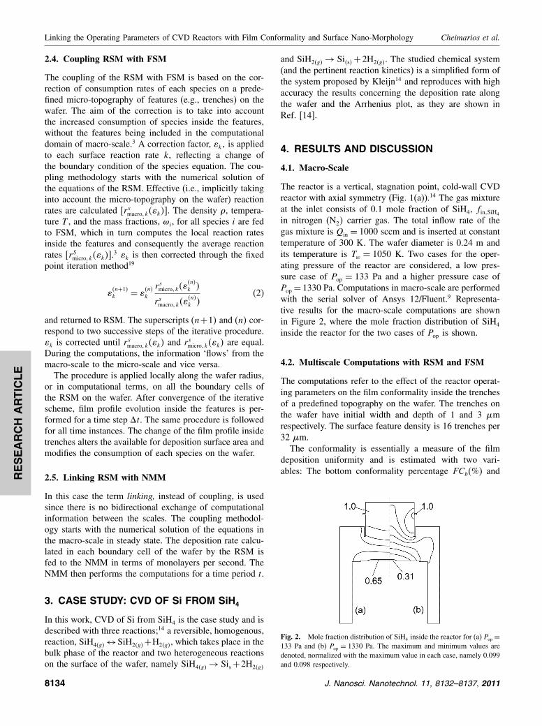
4.1. Macro-Scale
The reactor is a vertical, stagnation point, cold-wall CVDreactor with axial symmetry (Fig. 1(a)).14 The gas mixtureat the inlet consists of 0.1 mole fraction of SiH4, fin�SiH4
in nitrogen (N2� carrier gas. The total inflow rate of thegas mixture is Qin = 1000 sccm and is inserted at constanttemperature of 300 K. The wafer diameter is 0.24 m andits temperature is Tw = 1050 K. Two cases for the oper-ating pressure of the reactor are considered, a low pres-sure case of Pop = 133 Pa and a higher pressure case ofPop = 1330 Pa. Computations in macro-scale are performedwith the serial solver of Ansys 12/Fluent.9 Representa-tive results for the macro-scale computations are shownin Figure 2, where the mole fraction distribution of SiH4
inside the reactor for the two cases of Pop is shown.
4.2. Multiscale Computations with RSM and FSM
The computations refer to the effect of the reactor operat-ing parameters on the film conformality inside the trenchesof a predefined topography on the wafer. The trenches onthe wafer have initial width and depth of 1 and 3 mrespectively. The surface feature density is 16 trenches per32 m.The conformality is essentially a measure of the film
deposition uniformity and is estimated with two vari-ables: The bottom conformality percentage FCb(%) and
Fig. 2. Mole fraction distribution of SiH4 inside the reactor for (a) Pop =133 Pa and (b) Pop = 1330 Pa. The maximum and minimum values aredenoted, normalized with the maximum value in each case, namely 0.099and 0.098 respectively.
8134 J. Nanosci. Nanotechnol. 11, 8132–8137, 2011

RESEARCH
ARTIC
LE
Cheimarios et al. Linking the Operating Parameters of CVD Reactors with Film Conformality and Surface Nano-Morphology
the sidewall conformality percentage FCs(%), according tothe relation:
FCx�%�=(dx
dt
)·100 (3)
where x = b� s. The variables db�ds and dz represent thefilm thickness at three characteristic positions of the trenchand particularly at the middle of the bottom surface, atthe middle of the side surface and at the free surfacerespectively.The film conformality depends on the values of SE�SiH4
and SE�SiH2. SE� i is the effective sticking coefficient of
species i and expresses the probability for sticking, uponcollision with the surface, of species i� It comes from thesurface reaction kinetics.14 Low values of SE� i result inthe redistribution of flux inside the trench through the re-emissions’ mechanism. Lower values of SE� i result intohigher conformality. When SE� i = 0, every elementary sur-face receives the same amount of flux which results in auniform profile evolution of the film.The effect of the increase of Pop and the decrease of Qin
and fin�SiH4on film conformality are successively studied.
FCb and FCs are calculated at the instant the trenches arefilling at the conditions described in Table I.In Figure 3, the profile evolution of the film inside a
trench at the cluster of trenches extending from 0.0600 mto 0.0624 m from the center of the wafer is shown.Figure 3(a) corresponds to case (a) (see Table I) of reac-tor operating parameters. The void that is formed upon
Table I. The film conformality �FCb� FCs� inside the trenches under different operating conditions. rSiH4 and rSiH2 are the average rate of theheterogeneous reaction of SiH4 and SiH2 respectively and SE�SiH4
and SE�SiH2are the average effective sticking coefficients of SiH4 and SiH2, respectively.
The average quantities are reduced at the surface A (see Fig. 1(b)). All quantities are calculated at the trench filling instant.
Pop Ts Qin rSiH4 rSiH2 FCb FCs
Pa fin�SiH4 K sccm kmol ·m−2 s−1 SE�SiH4kmol ·m−2 s−1 SE�SiH4
% %
(a) 133 0.1 1050 1000 4.18 ·10−7 0.00294 3.50 ·10−9 1.0 91.8 91.6(b) 1033 0.1 1050 1000 6.66 ·10−7 0.00060 1.19 ·10−7 1.0 85.9 84.9(c) 133 0.1 1050 100 1.24 ·10−7 0.00560 4.19 ·10−10 1.0 81.3 81.3(d) 133 0.001 1050 1000 8.08 ·10−9 0.01499 9.95 ·10−12 1.0 67.4 67.2
Fig. 3. Profile evolution inside a trench at a cluster extending from 0.0600 m to 0.0624 m from the center of the wafer for the operating parametersshown in Table I. The profiles are presented for the equidistant time spaces of (a) 38.4 s, (b) 37 s, (c) 224 s and (d) 3120 s respectively.
trench filling is small which means that the conformalityis high, i.e., FCb and FCs are high (see Table I). To com-pare with case (a), a series of computations are performedto investigate the influence of the operating parameters ofthe reactor on the profile evolution of the film and theuniformity of deposition. In case (b), although increasingthe pressure leads to lower values of SE�SiH4
� FCb and FCs
decrease. The latter, unexpected result, is due to the highvalue of SE�SiH2
. Since, the average deposition rates of bothspecies are of the same order (see Table I), SE�SiH2
playsan important role and leads to the non-uniform depositionand the decrement of FCb and FCs. For the last two cases,by decreasing the mixture inlet flow [case (c)] and decreas-ing fin�SiH4
[case (d)], SE�SiH4increases. Thus, the void is
expanded [see Figs. 3(c–d)] and FCb and FCs decrease.In particular, in case (d) the maximum void is observedquantified with the minimum values of FCb and FCs.Besides the effects of the operating conditions on the
conformality, the effect of the topography on the deposi-tion rate of the film on the wafer is demonstrated. Theaverage deposition rate of the film versus the depositiontime for case (a) is presented in Figure 4. At the begin-ning of the computations (t = 0 sec), the trenches areempty and the deposition rate is lower than the depositionrate in the case without topography, due to the depletionof SiH4 and SiH2 coming from their increased consump-tion at the micro-topography (loading pahenomenon3). Asthe time elapses, the trenches are filling, the available for
J. Nanosci. Nanotechnol. 11, 8132–8137, 2011 8135

RESEARCH
ARTIC
LE
Linking the Operating Parameters of CVD Reactors with Film Conformality and Surface Nano-Morphology Cheimarios et al.
0 48 96 144 192 240
2.4
2.6
2.8
3.0
3.2
3.4
3.6
3.8
4.0
4.2
Trenches fill
Without topographyde
posi
tion
rate
×10
–3 (
Å/m
in)
time (s)
Fig. 4. The average deposition rate of the film versus time for reac-tor operating parameters Pop = 133 Pa, fin�SiH4 = 0�1, Tw = 1050 K andQin = 1000 sccm [case (a) in Table I].
deposition area decreases and the average deposition rateincreases. After trenches’ repletion the average depositionrate approaches the average rate for the case with flat wafersurface.
4.3. Multiscale Computations with RSM and NMM
The analysis concerns the nano-morphology of the film’ssurface during Si deposition on a Si(001) 2× 1 surface.A characteristic of the Si(001) 2×1 surface is the presenceof dimers; dimers’ formation is considered implicitly in theNMM through the implementation of an anisotropy in thediffusion energy barriers.15 The energy barrier for diffusion(see Eq. (1)) is given as E = Es +nEn +mEp, where Es
is the wafer contribution, and En and Ep are the in-planenearest neighbors contribution normal and parallel to thedimers formation, respectively, and n and m the number ofthe in-plane nearest neighbors normal and parallel to thedimers formation, respectively. The values of Es�En�Ep
and V0 are taken from Ref. [15]. The formation of thesedimers for the Si(001) 2× 1 surface has been reportedpreviously and is well established by experimental16 andtheoretical works.17
Si is deposited through the surface reactions reported inSection 3. The chosen operating conditions of the reactor�Pop = 1330 Pa, Tw = 1050 K) favor the epitaxial deposi-tion of Si.18 Due to the high Tw the hydrogen adsorption onthe surface is omitted.17 Even if the structure of the Si sur-face follows the diamond structure,18 we follow the workof Ref. [15] for the Si deposition where the computationsare performed in a simple cubic lattice.By applying the linking methodology described in
Section 2.5, the nano-morphology of the film’s surfacecan be constructed. Figure 5 shows the surface morphol-ogy of the growing crystal for 1.5 s of deposition time.Figures 5(a) and (b) show the surface morphology at themiddle and edge of the wafer. The center and the edge
Fig. 5. Surface nano-morphology after 1.5 s of deposition at (a) themiddle and (b) the edge of the wafer. The number of monolayersdeposited differs and leads to surfaces with different dimers orientation.
positions correspond to the maximum and minimum valueof the deposition rate computed from the RSM. Due tothe different values of the deposition rates at these twodistinct positions on the wafer, the number of monolay-ers deposited after 1.5 s differs and leads to surfaces withdifferent dimer orientation.In Figure 6 the surface roughness of the deposited film,
defined as the root mean square (RMS) deviation in thesurface height, is shown versus time for the first 0.1 s ofthe deposition. Figure 6 shows that the model can pre-dict the periodic change of the surface morphology15�17
manifested by the oscillations in the RMS value of thesurface height.
Fig. 6. RMS roughness at the middle of the wafer versus time duringthin film deposition.
8136 J. Nanosci. Nanotechnol. 11, 8132–8137, 2011

RESEARCH
ARTIC
LE
Cheimarios et al. Linking the Operating Parameters of CVD Reactors with Film Conformality and Surface Nano-Morphology
5. CONCLUSIONS AND FUTURE WORK
In this work, a multiscale computational framework is pre-sented to study the physical/chemical phenomena in theco-existing scales of CVD processes. The multiple scalesextent from cm in the bulk phase of the CVD reactor tom inside the features and nm in the growing surface ofthe film. Two types of problems are handled in the contextof CVD of Si from SiH4.In the first case, the computations illuminate the effects
of the reactor operating pressure, the inlet flow of the mix-ture and the mole fraction of the precursor on the depo-sition conformality of Si inside the trenches. The lowerconformality is reported when the mole fraction of SiH4
at the inlet is low.In the second case, the evolving nano-morphology of the
film is trailed. The computations reveal that the depositedfilm can have different dimer orientation along the waferdepending on the value of the deposition rate.Concerning the future aspects of our work, a more
detailed approach for NMM taking into account hydro-gen adsorption is under consideration.7�17 Moreover, cou-pling (instead of linking) of RSM with NMM will beused to explore the potential effect of the surface nano-morphology on the macro-scale.6
Acknowledgments: This work was partially supportedby the National Technical University of Athens throughthe Basic Research Program (�EBE-2007) and through afellowship to S. Garnelis and the State Scholarships Foun-dation through a fellowship to N. Cheimarios.
References and Notes
1. R. D. Braatz, R. C. Alkire, E. G. Seebauer, T. O. Drews, E. Rusli,M. Karulkar, F. Xue, Y. Qin, M. Y. L. Jung, and R. Gunawan, Comp.Chem. Eng. 30, 1643 (2006).
2. S. T. Rodgers and K. F. Jensen, J. Appl. Phys. 83, 524 (1998).3. N. Cheimarios, G. Kokkoris, and A. G. Boudouvis, Chem. Eng. Sci.
65, 5018 (2010).4. S. Kinoshita, S. Takagi, T. Kai, J. Shiozawa, and K. Maki, Jpn.
J. Appl. Phys. 44, 7855 (2005).5. L. Jaouen, F. Roqueta, E. Scheid, H. Vergnes, and B. Caussat, Pro-
ceedings – Electrochemical Society PV 2005-09, 111 (2005).6. R. Lam and D. G. Vlachos, Phys. Rev. B 6403, 035401 (2001).7. C. Cavallotti, E. Pantano, A. Veneroni, and M. Masi, Cryst. Res.
Technol. 40, 958 (2005).8. T. C. Xenidou, N. Prud’homme, C. Vahlas, N. C. Markatos, and
A. G. Boudouvis, J. Electrochem. Soc. 157, D633 (2010).9. Ansys v12.1, ANSYS Inc, http://www.ansys.com/.10. T. S. Cale and G. B. Raupp, J. Vac. Sci. Technol. B 8, 1242
(1990).11. G. Kokkoris, A. G. Boudouvis, and E. Gogolides, J. Vac. Sci. Tech-
nol. A 24, 2008 (2006).12. G. Kokkoris, A. Tserepi, A. G. Boudouvis, and E. Gogolides, J. Vac.
Sci. Technol. A 22, 1896 (2004).13. K. A. Fichthorn and W. H. Weinberg, J. Chem. Phys. 95, 1090
(1991).14. C. R. Kleijn, J. Electrochem. Soc. 138, 2190 (1991).15. M. R. Wilby, S. Clarke, T. Kawamura, and D. D. Vvedensky, Phys.
Rev. B 40, 10617 (1989).16. R. J. Hamers, U. K. Kohler, and J. E. Demuth, Ultramicroscopy
31, 10 (1989).17. K. Satake and D. B. Graves, J. Chem. Phys. 118, 6503 (2003).18. J. Plummer, M. Deal, and P. B. Griffin, Silicon VLSI Technology:
Fundamentals, Practice, and Modeling, Prentice Hall, New York(2000).
19. N. Cheimarios, G. Kokkoris, and A. G. Boudouvis, App. Num. Math.(2011), doi:10.1016/j.apnum.2011.07.002.
Received: 9 May 2011. Accepted: 24 June 2011.
J. Nanosci. Nanotechnol. 11, 8132–8137, 2011 8137