linear regulators selection guide · fpj : to252-j5 fp2 : to263-5 to263-3 fp3 : sot223-4 w enable...
TRANSCRIPT

www.rohm.com
LINEAR REGULATORS SELECTION GUIDE
LDO, 3-terminal regulator Rev. 3.0
2017-2018

LINEAR REGULATORS SELECTION GUIDE www.rohm.com
1
Table of Contents
Multi-Output LDO Regulators
Single-Output Linear Regulators
3-Terminal Regulators
LDO 45 V, 50 V rating
Products Table
LDO 7 V, 10 V and 15 V rating
CMOS LDO 5.5 V-6.5 V rating
LDO 18 V, 35 V rating
Package
2
3
5
7
9
11
15
21
29
Selection Guide by Function
Ultra LDO Type Regulators 13
LDO+ (Plus) 22
Termination Regulators for DDR SDRAM 25
Ultra Low Noise LDO for Audio 27
This selection guide features linear regulators.
ROHM’s linear regulators come in a wide lineup of general-purpose 3-terminal models,
low dropout (LDO) models, low power consumption models, large current models and
high voltage models. They are applied to power circuits of cellular phones, automotive
devices, home electric appliances, consumer equipment and industrial.
ROHM Website
For ROHM’s power supply IC lineup, visit the following ROHM website.
http://www.rohm.com
ROHM provides design and technical data and tools such as data sheets, application
notes, reference designs and Spice model.
http://micro.rohm.com/en/techweb http://deviceplus.com
Before using a ROHM IC, be sure to check its setting values, data and functions against the latest data sheet.

LINEAR REGULATORS SELECTION GUIDE www.rohm.com
2
0.1-0.15 0.2 0.3 0.5-0.55 1.0 1.5 2.0 3.0 4.0External
MOSFET
45-50
BD7xxL2
BD3010A
BD4xxM2
BD4269FJ BD4269EFJ
BD7xxL5
BD357xY
BD3020
BD3021
BD4xxM5
BD42754
30-36
BDxxFA1 BD3650 BA78Mxx BA78xx
BAxxCC0
BDxxC0A
BDxxFC0
BAxxDD0BD00D0ABDxxFD0
18
BAxxBC0
BD37210
BD37215(負)
BAxxJC5
15BDxxGA3 BDxxGA5 BDxxGC0
BA1117
10 BDxxHA3 BDxxHA5 BDxxHC0 BDxxHC5
6.0-7.0
BHxxNB1
BHxxPB1
BHxxRB1
BHxxSA3
BUxxJA2
BUxxSA4
BUxxSD2
BUxxTA2
BUxxTD2
BUxxTD3
BHxxM0A BDxxIA5
BDxxKA5
BUxxSA5
BUxxSD5
BD37201
BDxxIC0
6.0-7.0
BD3507
BD3540
BD3550
BD3541
BD3551
BD3506
BD3552
BD3508
BD3512
BD3509 BD3504
BD3521
Single-Output Linear Regulators – Products Table
Output current (A)
Input voltage r
ating (
V)
General
application
High voltage for automotive
and industrial
Low voltage/Low current for
portable equipment
Ultra-low voltage/Large
current for CPU/DSP (Dual
power supply system)

LINEAR REGULATORS SELECTION GUIDE www.rohm.com
3
VIN max : 35V
VIN : 7.5 V to 33 V
Io : 1A
Vo : 5V, 6V, 7V, 8V, 9V, 10V,
12V, 15V, 18V, 20V, 24V
Output tolerance: 4%
Overcurrent protection
Thermal protection
Safe operating range limiting circuit
TO252-3
78xx
Series
78Mxx
Series
VIN max : 35V
VIN : 7.5 V to 33 V
Io : 500mA
Vo : 5V, 6V, 7V, 8V, 9V, 10V,
12V, 15V, 18V, 20V, 24V
Output tolerance: 4%
Overcurrent protection
Thermal protection
Safe operating range limiting circuit
78Lxx
Series
VIN max : 30V
VIN : (Vo+3)V to 25V
Io : 100mA
Vo : 3.3V, 5V, 5.4V, 12V
Output tolerance: 1%
Output ceramic capacitor supported
Soft start
Overcurrent protection
Thermal protection
1117
Series
VIN max : 15V
VIN : 2.65V to 10V
Io : 1A
Vo: Variable from 1.25 V to 8.6 V
Output tolerance: 1%
Output ceramic capacitor supported
Overcurrent protection
Thermal protection
VIN INPUT
COMMON
OUTPUT VOUTINPUT
COMMON
OUTPUT
TO220CP-3
TO252-3
VIN INPUT
COMMON
OUTPUT VOUTINPUT
COMMON
OUTPUT
TO220CP-3
SOT89-3K
VIN INPUT
COMMON
OUTPUT VOUTVcc
GND
Vo
TO252-3
VIN INPUT
COMMON
OUTPUT VOUTVIN
ADJ
VOUT
Pin-compatible
μA78xx, AS78xx, SP78xx, LM78xx,
KA78xx, MC78xx, IFX78xx, NJM78xx,
NCV78xx, L78xx, TA78xx etc.
Pin-compatible
μA78Mxx, MC78Mxx, LM78Mxx,
KA78Mxx, IFX78Mxx, NJM78Mxx,
AN78Mxx, L78Mxx, TA78Mxx etc.
Pin-compatible
μA78Lxx, AS78Lxx, AP78Lxx,
ZR78Lxx, SP78Lxx, MC78Lxx,
LM78Lxx, KA78Lxx, NJM78Lxx,
AN78Lxx, L78Lxx, TA78Lxx etc.
Pin-compatible
LM1117, AP1117, ZLDO1117,
AZ1117, SPX1117, RC1117,
FAN1117, IFX1117, IRU1117, LT1117,
NX1117 etc.
BA78xx Series BA78Mxx Series BDxxFA1 Series BA1117
3-Terminal Regulators
LINEAR REGULATORS SELECTION GUIDE www.rohm.com
4
3-Terminal Regulators
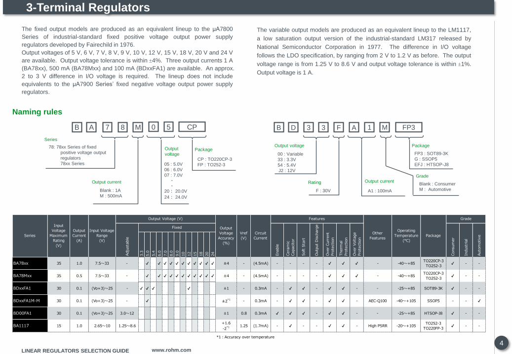
The fixed output models are produced as an equivalent lineup to the μA7800
Series of industrial-standard fixed positive voltage output power supply
regulators developed by Fairechild in 1976.
Output voltages of 5 V, 6 V, 7 V, 8 V, 9 V, 10 V, 12 V, 15 V, 18 V, 20 V and 24 V
are available. Output voltage tolerance is within 4%. Three output currents 1 A
(BA78xx), 500 mA (BA78Mxx) and 100 mA (BDxxFA1) are available. An approx.
2 to 3 V difference in I/O voltage is required. The lineup does not include
equivalents to the μA7900 Series’ fixed negative voltage output power supply
regulators.
Naming rules
The variable output models are produced as an equivalent lineup to the LM1117,
a low saturation output version of the industrial-standard LM317 released by
National Semiconductor Corporation in 1977. The difference in I/O voltage
follows the LDO specification, by ranging from 2 V to 1.2 V as before. The output
voltage range is from 1.25 V to 8.6 V and output voltage tolerance is within 1%.
Output voltage is 1 A.
B A 7 8 M 0
Series
78: 78xx Series of fixed
positive voltage output
regulators
78xx Series
Output
voltage
05 : 5.0V
06 : 6.0V
07 : 7.0V
・・
20: 20.0V
24: 24.0V
Output current
Blank : 1A
M : 500mA
5 CP
Package
CP : TO220CP-3
FP : TO252-3
B D 3 3 F A 1
Output current
A1 : 100mA
Rating
F : 30V
Output voltage
00 : Variable
33 : 3.3V
54 : 5.4V
J2 : 12V
FP3
Package
FP3 : SOT89-3K
G : SSOP5
EFJ : HTSOP-J8
M
Blank : Consumer
M : Automotive
Grade
3.3
5.0
5.4
6.0
7.0
8.0
9.0
10
12
15
18
20
24
BA78xx 35 1.0 7.5~33 - ✔ ✔ ✔ ✔ ✔ ✔ ✔ ✔ ✔ ✔ ✔ ±4 - (4.5mA) - - - - ✔ ✔ ✔ - -40~+85TO220CP-3
TO252-3✔ - -
BA78Mxx 35 0.5 7.5~33 - ✔ ✔ ✔ ✔ ✔ ✔ ✔ ✔ ✔ ✔ ✔ ±4 - (4.5mA) - - - - ✔ ✔ ✔ - -40~+85TO220CP-3
TO252-3✔ - -
BDxxFA1 30 0.1 (Vo+3)~25 - ✔ ✔ ✔ ✔ ±1 - 0.3mA - ✔ ✔ - ✔ ✔ - - -25~+85 SOT89-3K ✔ - -
BDxxFA1M-M 30 0.1 (Vo+3)~25 - ✔ ±2*1 - 0.3mA - ✔ ✔ - ✔ ✔ - AEC-Q100 -40~+105 SSOP5 - - ✔
BD00FA1 30 0.1 (Vo+3)~25 3.0~12 ±1 0.8 0.3mA ✔ ✔ ✔ - ✔ ✔ - - -25~+85 HTSOP-J8 ✔ - -
BA1117 15 1.0 2.65~10 1.25~8.6+1.6
-2*1 1.25 (1.7mA) - ✔ - - ✔ ✔ - High PSRR -20~+105TO252-3
TO220FP-3✔ - -
Series
Input
Voltage
Maximum
Rating
(V)
Output
Current
(A)
Input Voltage
Range
(V)
Output Voltage (V)
Output
Voltage
Accuracy
(%)
Vref
(V)
Circuit
Current
Features
Over
Curr
ent
Pro
tect
ion
Therm
al
Pro
tect
ion
Over
Voltage
Pro
tect
ion
Consu
mer
Indust
rial
Auto
motivePackage
Grade
*1:Accuracy over temperature
Adju
stable
Fixed
Enable
Cera
mic
Capaci
tor
Soft
Sta
rt
Outp
ut
Dis
charg
e
Other
Features
Operating
Temperature
(°C)
LINEAR REGULATORS SELECTION GUIDE www.rohm.com
5
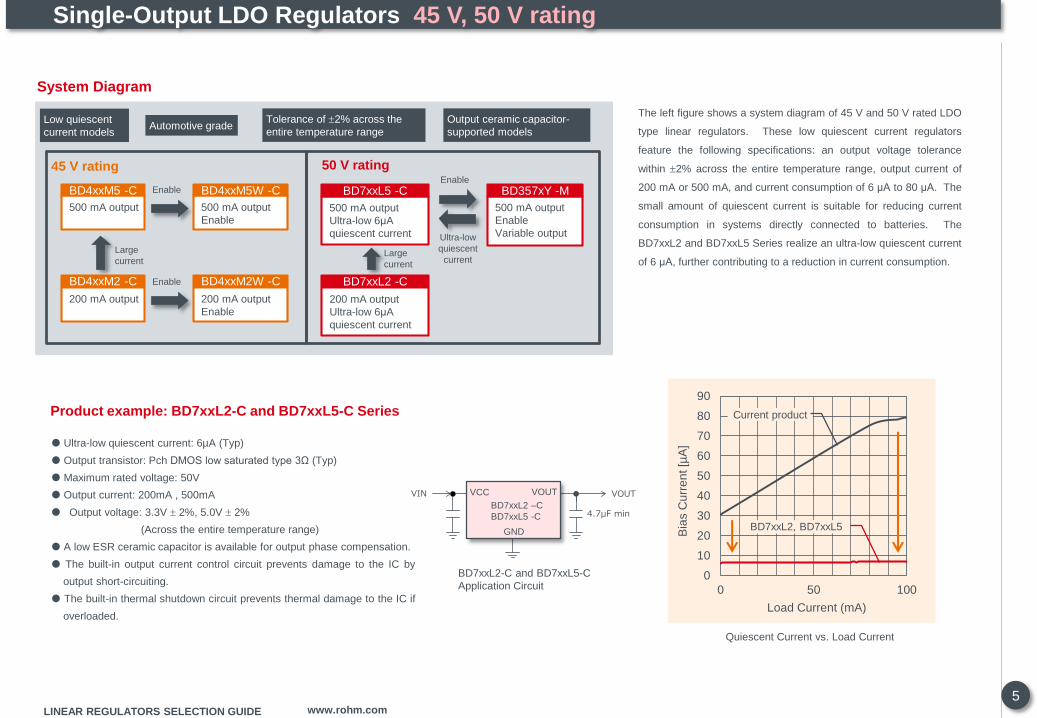
Single-Output LDO Regulators 45 V, 50 V rating
The left figure shows a system diagram of 45 V and 50 V rated LDO
type linear regulators. These low quiescent current regulators
feature the following specifications: an output voltage tolerance
within 2% across the entire temperature range, output current of
200 mA or 500 mA, and current consumption of 6 μA to 80 μA. The
small amount of quiescent current is suitable for reducing current
consumption in systems directly connected to batteries. The
BD7xxL2 and BD7xxL5 Series realize an ultra-low quiescent current
of 6 μA, further contributing to a reduction in current consumption.
Automotive gradeTolerance of 2% across the
entire temperature range
Low quiescent
current models
Output ceramic capacitor-
supported models
45 V rating
200 mA output
500 mA output
Enable
Enable
200 mA output
Enable
500 mA output
Enable
200 mA output
Ultra-low 6μA
quiescent current
500 mA output
Ultra-low 6μA
quiescent current
Large
current
500 mA output
Enable
Variable output
Enable
Ultra-low
quiescent
current
BD4xxM5W -CBD4xxM5 -C
BD4xxM2W -CBD4xxM2 -C BD7xxL2 -C
BD7xxL5 -C BD357xY -M
50 V rating
Large
current
System Diagram
Product example: BD7xxL2-C and BD7xxL5-C Series
Ultra-low quiescent current: 6µA (Typ)
Output transistor: Pch DMOS low saturated type 3Ω (Typ)
Maximum rated voltage: 50V
Output current: 200mA , 500mA
Output voltage: 3.3V 2%, 5.0V 2%
(Across the entire temperature range)
A low ESR ceramic capacitor is available for output phase compensation.
The built-in output current control circuit prevents damage to the IC by
output short-circuiting.
The built-in thermal shutdown circuit prevents thermal damage to the IC if
overloaded.
BD7xxL2-C and BD7xxL5-C
Application Circuit
VIN VCC
GND
VOUT
4.7μF min
VOUTVCC
GND
VOUT
BD7xxL2 –C
BD7xxL5 -C
Quiescent Current vs. Load Current
0
10
20
30
40
50
60
70
80
90
0 50 100
Bia
s C
urr
en
t [µ
A]
Load Current (mA)
Current product
BD7xxL2, BD7xxL5

LINEAR REGULATORS SELECTION GUIDE www.rohm.com
6
Naming rules
B D 3 5 7 0 Y FP
Package
FP : TO252-3
TO252-5
HFP : HRP5
Function
0 : Vo=3.3V, Enable=OFF
1 : Vo=5.0V, Enable=OFF
2 : Vo=Variable, Enable=OFF
3 : Vo=3.3V, Enable=ON
4 : Vo=5.0V, Enable=ON
5 : Vo=Variable, Enable=ON
B D 7 3 3 L 2
Output current
2 : 200mA
5 : 500mA
Rating
4 : 45V
7 : 50V
Output voltage
33 : 3.3V
50 : 5.0V
EFJ
Package
EFJ : HTSOP-J8
FP : TO252-3
FPJ : TO252-J5
FP2 : TO263-5
TO263-3
FP3 : SOT223-4
W
Enable
Blank : OFF
W : ON
Current consumption
M : Low quiescent current
L : Ultra-low quiescent current
Single-Output LDO Regulators 45 V, 50 V rating
1.2
1.5
1.8
2.5
3.0
3.3
5.0
6.0
7.0
8.0
9.0
10
12
BD357xY -M 50 0.5 4.5~36 2.8~12 ✔ ✔ ±2*1 1.26 30μA ✔ ✔ ✔ ✔ - -40~+125
TO252-3
HRP5
TO252-5
- - ✔
BD7xxL5 -C 50 0.5 4.17~45 - ✔ ✔ ±2*1 - 6μA - ✔ ✔ ✔ AEC-Q100 -40~+125 TO252-3 - - ✔
BD7xxL2 -C 50 0.2 4.37~45 - ✔ ✔ ±2*1 - 6μA - ✔ ✔ ✔ AEC-Q100 -40~+125
HTSOP-J8
TO252-3
SOT223-4
- - ✔
BD4xxM5 -C 45 0.5 4.0~42 - ✔ ✔ ±2*1 - 38μA - ✔ ✔ ✔ AEC-Q100
Tj
-40~+150
TO252-3
TO263-3- - ✔
BD4xxM5W -C 45 0.5 4.0~42 - ✔ ✔ ±2*1 - 38μA ✔ ✔ ✔ ✔ AEC-Q100Tj
-40~+150
TO252-J5
TO263-5- - ✔
BD4xxM2 -C 45 0.2 3.9~42 - ✔ ✔ ±2*1 - 40μA - ✔ ✔ ✔ AEC-Q100
Tj
-40~+150
HTSOP-J8
SOT223-4- - ✔
BD4xxM2W -C 45 0.2 3.9~42 - ✔ ✔ ±2*1 - 40μA ✔ ✔ ✔ ✔ AEC-Q100Tj
-40~+150
HTSOP-J8
SOT223-4- - ✔
Series
Input
Voltage
Maximum
Rating
(V)
Output
Current
(A)
Input
Voltage
Range
(V)
Output Voltage (V)
Output
Voltage
Accuracy
(%)
Vref
(V)
Circuit
Current
Features
Adju
stable
Fixed
Enable
Cera
mic
Capaci
tor
Indust
rial
Auto
motive
Other
Features
Operating
Temperature
(°C)
Package
Grade
*1:Accuracy over temperatureO
ver
Curr
ent
Pro
tect
ion
Therm
al
Pro
tect
ion
Consu
mer

LINEAR REGULATORS SELECTION GUIDE www.rohm.com
7
Single-Output LDO Regulators 18 V, 35 V rating
BDxxC0A
±1% tolerance
1 A output
-40°C~+105°C
35 V rating
BDxxC0AW
±1% tolerance
1 A output
Enable
Variable output
-40°C~+105°C
Tolerance of 3% across
the entire temperature
range precision
1 A output
-40°C~+125°C
BAxxCC0
±2% tolerance
1 A output
BAxxCC0W
±2% tolerance
1 A output
Enable
Variable output
Ceramic capacitor supported
High precision
With enable function
BDxxFC0W
±1% tolerance
1 A output
Enable
Variable output
-25°C~+85°C
±1% tolerance
2 A output
±1% tolerance
2 A output
Enable
Variable output
BD00D0AW
±1% tolerance
2 A output
Enable
Variable output
-40°C~+105°C
Tolerance of 2% across
the entire temperature
range precision
300 mA output
-40°C~+125°C
Output ceramic capacitor-
supported models
With enable function
Ceramic
capacitor
supported
Large
current
High
precision
Automo
tive
grade
Automoti
ve grade
BDxxC0AW -C
Tolerance of 3% across
the entire temperature
range precision
1 A output
Enable
-40°C~+125°C
Automo
tive
grade
BAxxBC0
±2% tolerance
1 A output
±2% tolerance
1.5 A output
Large
currentBAxxBC0W
±2% tolerance
1 A output
Enable
Variable output
With enable function
±2% tolerance
1.5 A output
Enable
Variable output
With enable function
18 V rating
BAxxJC5W
BAxxJC5 BAxxDD0
BAxxDD0W
BD3650 -M
BDxxC0A -C
BDxxFC0
±1% tolerance
1 A output
Variable output
-25°C~+85°C
BDxxFD0W
±1% tolerance
2 A output
Enable
Variable output
-25°C~+85°C
Wide operating
temperature
range
Ceramic
capacitor
supported
High
precision
Wide operating
temperature
range
Wide operating
temperature
range
System Diagram
Naming rules B D 3 3 C 0 A
Rating, Output
currentBC0 : 18V, 1A
JC5 : 18V, 1.5A
FC0 : 35V, 1A
CC0 : 35V, 1A
C0A : 35V, 1A
FD0 : 35V, 2A
DD0 : 35V, 2A
D0A : 35V, 2A
Output voltage
00 : 可変15 : 1.5V
・・
90 : 9.0V
J0 : 10.0V
J2 : 12.0V
FP
Package
T : TO220FP-5
TO220FP-3
TO220FP-5(V5)
CP : TO220CP-V5
FP : TO252-3
TO252-5
W
Enable
Blank : OFF
W: ON
BA : Bipolar
BD : BiCDMOS
Process
HFP : HRP5
FP2 : TO263-3
TO263-5
EFJ : HTSOP-J8

LINEAR REGULATORS SELECTION GUIDE www.rohm.com
8
Single-Output LDO Regulators 18 V, 35 V rating
1.0
1.2
1.2
5
1.5
1.8
2.5
2.6
3.0
3.3
5.0
6.0
7.0
8.0
9.0
10
12
15
16
BD3650 -M 36 0.3 5.6~30 - ✔ ±2*1 - 0.5mA - ✔ - - ✔ ✔ - - -40~+125 TO252-3 - - ✔
BDxxFD0W 35 2.0 4.0~32 1.5~16 ✔ ✔ ✔ ✔ ✔ ✔ ✔ ✔ ✔ ✔ ✔ ±1 0.75 0.5mA ✔ ✔ - - ✔ ✔ - - -25~+85 HRP5 ✔ - -
BAxxDD0 35 2.0 3.0~25 - ✔ ✔ ✔ ✔ ✔ ✔ ✔ ✔ ✔ ✔ ±1 - 0.9mA - - - - ✔ ✔ ✔ - -40~+125 TO220FP-3 ✔ - -
BAxxDD0W 35 2.0 3.0~25 1.5~16 ✔ ✔ ✔ ✔ ✔ ✔ ✔ ✔ ✔ ±1 1.27 0.9mA ✔ - - - ✔ ✔ ✔ - -40~+125
TO220CP-V5
TO220FP-5
HRP5
✔ - -
BD00D0AW 35 2.0 4.0~25 3.0~15 ±1 0.75 0.5mA ✔ ✔ - - ✔ ✔ - - -40~+105 HRP5 ✔ - -
BDxxFC0 35 1.0 4.0~26.5 1.0~15 ✔ ✔ ±1 0.75 0.5mA - ✔ - - ✔ ✔ - - -25~+85 TO252-3 ✔ - -
BDxxFC0W 35 1.0 4.0~26.5 1.0~15 ✔ ✔ ✔ ✔ ✔ ✔ ✔ ✔ ✔ ✔ ±1 0.75 0.5mA ✔ ✔ - - ✔ ✔ - - -25~+85HTSOP-J8
TO252-5✔ - -
BAXXCC0 35 1.0 4.0~25 - ✔ ✔ ✔ ✔ ✔ ✔ ✔ ✔ ✔ ✔ ±2 - 2.5mA - - - - ✔ ✔ ✔ - -40~+125TO220FP-3
TO252-3✔ - -
BAxxCC0W 35 1.0 4.0~25 3.0~15 ✔ ✔ ✔ ✔ ✔ ✔ ✔ ✔ ✔ ±2 1.225 2.5mA ✔ - - - ✔ ✔ ✔ - -40~+125
TO220CP-V5
TO220FP-5
TO252-5
✔ - -
BDxxC0A
BDxxC0A -C35 1.0
VO+1.0
~26.5-
✔ ✔
✔
✔
✔
✔
±1
±3*1 - 0.5mA - ✔ - - ✔ ✔ - AEC-Q100-40~+105
-40~+125
TO252S-3
TO252-3
HRP5
TO263-3
✔
-
-
-
-
✔
BDxxC0AW
BDxxC0AW -M
BDxxC0AW -C
35 1.0VO+1.0
~26.5
3.0~15
3.0~15
1.0~15
✔
✔
✔
✔ ✔ ✔
±1
±3*1
±3*1
0.75 0.5mA ✔ ✔ - - ✔ ✔ - AEC-Q100
-40~+105
-40~+105
-40~+125
TO252-5
TO220CP-V5
HRP5
TO263-5
✔
-
-
-
-
-
-
✔
✔
BAxxJC5 18 1.5 3.0~16 - ✔ ✔ ✔ ✔ ✔ ✔ ✔ ✔ ✔ ✔ ±1 - 0.5mA - - - - ✔ ✔ - - -40~+105 TO220FP-3 ✔ - -
BA00JC5W 18 1.5 3.0~16 1.5~12 ±1 1.25 0.5mA ✔ - - - ✔ ✔ - - -40~+105 TO220FP-5 ✔ - -
BAxxBC0 18 1.0 3.0~16 - ✔ ✔ ✔ ✔ ✔ ✔ ✔ ✔ ✔ ✔ ✔ ±2 - 0.5mA - - - - ✔ ✔ - - -40~+105TO252-3
TO220FP-3✔ - -
BAxxBC0W 18 1.0 3.0~16 1.5~12 ✔ ✔ ✔ ✔ ✔ ✔ ✔ ✔ ✔ ✔ ✔ ±2 1.25 0.5mA ✔ - - - ✔ ✔ - - -40~+105
TO252-5
TO220FP-5
TO220CP-V5
✔ - -
Outp
ut
Dis
charg
e
Series
Input
Voltage
Maximum
Rating
(V)
Output
Current
(A)
Input
Voltage
Range
(V)
Output Voltage (V)
Output
Voltage
Accuracy
(%)
Vref
(V)
Circuit
Current
Features
Adju
stable
Fixed
Enable
Cera
mic
Capaci
tor
Soft
Sta
rt
Auto
motive
Other
Features
Operating
Temperature
(°C)
Package
Grade
Over
Curr
ent
Pro
tect
ion
Therm
al
Pro
tect
ion
Over
Voltage
Pro
tect
ion
Consu
mer
Indust
rial
*1:Accuracy over temperature

LINEAR REGULATORS SELECTION GUIDE www.rohm.com
9
BDxxGA3W15 V rating
Large current
BDxxGA5W15 V rating
BDxxGC0W15 V rating
BDxxHA3M -LB10 V rating
BDxxHA3M -M10 V rating
BDxxGA5M -LB15 V rating
BDxxGA5M -M15 V rating
BDxxGC0M -LB15 V rating
BDxxIC0M -M7 V rating
Automotive grade
BDxxHC5M -LB10 V rating
BDxxHC5M -M10 V rating
Industrial gradeBDxxHC5W10 V rating
Large current
Large current
Automotive grade
Output ceramic capacitor-supported models
Industrial grade
Tolerance of 3% across the
entire temperature rangeModels with enable function
1% tolerance
1.5 A output
1 A output
500 mA output
300 mA output
BDxxHC0W10 V rating
BDxxIC0W7 V rating
BDxxHA5W10 V rating
BDxxIA5W7 V rating
BDxxHA3W10 V rating
BDxxHC0M -M10 V rating
BDxxGC0M -M15 V rating
BDxxHC0M -LB10 V rating
BDxxIC0M -LB7 V rating
BDxxGA3M -LB15 V rating
BDxxGA3M -M15 V rating
BDxxHA5M -M10 V rating
BDxxIA5M -M7 V rating
BDxxHA5M -LB10 V rating
BDxxIA5M -LB7 V rating
BDxxKA5W7 V rating
Small size
With enable
function
BDxxKA57 V rating
System Diagram
B D 1 5 C 0
Output current
C5 : 1.5A
C0 : 1A
A5 : 500mA
A3 : 300mA
Output voltage
00 : Variable
15 : 1.5V
18 : 1.8V
・・
90 : 9.0V
J0 : 10.0V
J2 : 12.0V
EFJ
Package
EFJ : HTSOP-J8
NUX : VSON008X2030
FP : TO252-3
FP : TO252-5
F : SOP8
HFV : HVSOF6
W
Enable
Blank : OFF
W: ON
M: ON (Vehicle parts)
H
Rating
G : 15V
H : 10V
I : 7V
Naming rules
The left figure shows a system diagram of 7 V, 10 V
and 15 V rated LDO type linear regulators. These
models feature output currents of 300 mA, 500 mA,
1 A and 1.5 A, and come in automotive and
industrial grades. An output voltage tolerance of
3% is ensured for both grades across the entire
temperature range.
Single-Output LDO Regulators 7 V, 10 V and 15 V rating
Automotive gradeIndustrial grade
Automotive gradeIndustrial grade
Automotive gradeIndustrial grade
KA5 : 7V, 500mA

LINEAR REGULATORS SELECTION GUIDE www.rohm.com
10
Single-Output LDO Regulators 7 V, 10 V and 15 V rating
1.0
1.2
1.2
5
1.5
1.8
2.5
2.6
3.0
3.3
5.0
6.0
7.0
8.0
9.0
10
12
15
16
BDxxGC0W
BDxxGC0M -LB
BDxxGC0M -M
15 1.0 4.5~14 1.5~13 ✔ ✔ ✔ ✔ ✔ ✔ ✔ ✔ ✔ ✔ ✔ ✔
±1
±3*1
±3*1
0.8 0.6mA ✔ ✔ ✔ - ✔ ✔ -
-
-
AEC-Q100
-25~+85
-40~+105
-40~+105
HTSOP-J8
✔
-
-
-
✔
-
-
-
✔
BDxxGA5W
BDxxGA5M -LB
BDxxGA5M -M
15 0.5 4.5~14 1.5~13 ✔ ✔ ✔ ✔ ✔ ✔ ✔ ✔ ✔ ✔ ✔ ✔
±1
±3*1
±3*1
0.8 0.6mA ✔ ✔ ✔ - ✔ ✔ -
-
-
AEC-Q100
-25~+85
-40~+105
-40~+105
HTSOP-J8
✔
-
-
-
✔
-
-
-
✔
BDxxGA3W 15 0.3 4.5~14 1.5~13 ✔ ✔ ✔ ✔ ✔ ✔ ✔ ✔ ✔ ✔ ✔ ✔ ±1 0.8 0.6mA ✔ ✔ ✔ - ✔ ✔ - - -25~+85HTSOP-J8
VSON008X2030✔ - -
BDxxGA3M -LB
BDxxGA3M -M15 0.3 4.5~14 1.5~13 ✔ ✔ ✔ ✔ ✔ ✔ ✔ ✔ ✔ ✔ ✔ ✔ ±3*1 0.8 0.6mA ✔ ✔ ✔ - ✔ ✔ -
-
AEC-Q100-40~+105 HTSOP-J8
-
-
✔
-
-
✔
BDxxHC5W
BDxxHC5M -LB
BDxxHC5M -M
10 1.5 4.5~8.0 1.5~7.0 ✔ ✔ ✔ ✔ ✔ ✔ ✔ ✔
±1
±3*1
±3*1
0.8 0.6mA ✔ ✔ ✔ - ✔ ✔ -
-
-
AEC-Q100
-25~+85
-40~+105
-40~+105
HTSOP-J8
✔
-
-
-
✔
-
-
-
✔
BDxxHC0W
BDxxHC0M -LB
BDxxHC0M -M
10 1.0 4.5~8.0
0.8~7.0
1.5~7.0
1.5~7.0
✔ ✔ ✔ ✔ ✔ ✔ ✔ ✔
±1
±3*1
±3*1
0.8 0.6mA ✔ ✔ ✔ - ✔ ✔ -
-
-
AEC-Q100
-25~+85
-40~+105
-40~+105
HTSOP-J8
✔
-
-
-
✔
-
-
-
✔
BDxxHA5W
BDxxHA5M -LB
BDxxHA5M -M
10 0.5 4.5~8.0 1.5~7.0 ✔ ✔ ✔ ✔ ✔ ✔ ✔ ✔
±1
±3*1
±3*1
0.8 0.6mA ✔ ✔ ✔ - ✔ ✔ -
-
-
AEC-Q100
-25~+85
-40~+105
-40~+105
HTSOP-J8
✔
-
-
-
✔
-
-
-
✔
BDxxHA3W
BDxxHA3M -LB
BDxxHA3M -M
10 0.3 4.5~8.0 1.5~7.0 ✔ ✔ ✔ ✔ ✔ ✔ ✔ ✔
±1
±3*1
±3*1
0.8 0.6mA ✔ ✔ ✔ - ✔ ✔ -
-
-
AEC-Q100
-25~+85
-40~+105
-40~+105
HTSOP-J8
✔
-
-
-
✔
-
-
-
✔
BDxxIC0W 7 1.0 2.4~5.5 0.8~4.5 ✔ ✔ ✔ ✔ ✔ ✔ ✔ ✔ ✔ ±1 0.8 0.25mA ✔ ✔ ✔ - ✔ ✔ - - -25~+85HVSOF6
HTSOP-J8✔ - -
BDxxIC0M -LB
BDxxIC0M -M7 1.0 2.4~5.5 0.8~4.5 ✔ ✔ ✔ ✔ ✔ ✔ ✔ ±3
*1 0.8 0.25mA ✔ ✔ ✔ - ✔ ✔ --
AEC-Q100-40~+105 HTSOP-J8
-
-
✔
-
-
✔
BDxxIA5W
BDxxIA5M -LB
BDxxIA5M -M
7 0.5 2.4~5.5 0.8~4.5 ✔ ✔ ✔ ✔ ✔ ✔ ✔
±1
±3*1
±3*1
0.8 0.25mA ✔ ✔ ✔ - ✔ ✔ -
-
-
AEC-Q100
-25~+85
-40~+105
-40~+105
HTSOP-J8
✔
-
-
-
✔
-
-
-
✔
BDxxKA5 7 0.5 2.3~5.5 - ✔ ✔ ✔ ✔ ✔ ✔ ✔ ±1 - 0.35mA - ✔ - - ✔ ✔ - - -40~+105 TO252-3 ✔ - -
BDxxKA5W 7 0.5 2.3~5.5 1.0~4.0 ✔ ✔ ✔ ✔ ✔ ✔ ✔ ±1 0.75 0.35mA ✔ ✔ - - ✔ ✔ - - -40~+105TO252-5
SOP8✔ - -
*1:Accuracy over temperature
Over
Curr
ent
Pro
tect
ion
Therm
al
Pro
tect
ion
Over
Voltage
Pro
tect
ion
Consu
mer
Outp
ut
Dis
charg
e
Indust
rial
Auto
motiveOther
Features
Operating
Temperature
(°C)
Package
Grade
Series
Input
Voltage
Maximum
Rating
(V)
Output
Current
(A)
Input
Voltage
Range
(V)
Output Voltage (V)
Output
Voltage
Accuracy
(%)
Vref
(V)
Circuit
Current
Features
Adju
stable
Fixed
Enable
Cera
mic
Capaci
tor
Soft
Sta
rt
LINEAR REGULATORS SELECTION GUIDE www.rohm.com
11
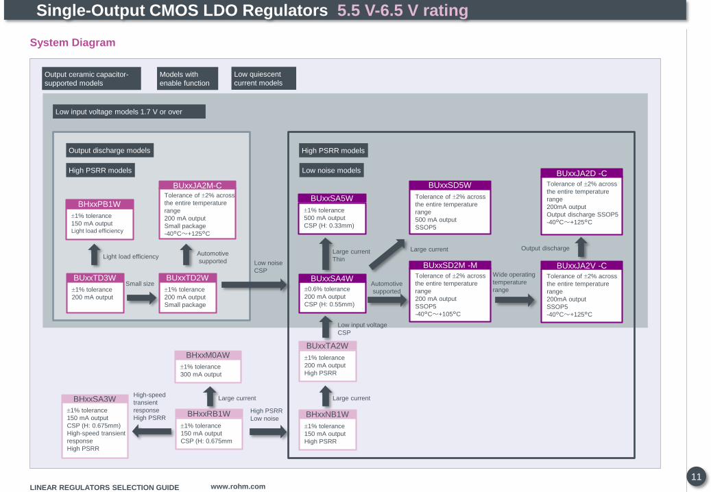
Single-Output CMOS LDO Regulators 5.5 V-6.5 V rating
System Diagram
1% tolerance
150 mA outputLight load efficiency
BUxxTD3W
1% tolerance
200 mA output
Small sizeBUxxTD2W
1% tolerance
200 mA output
Small package
Low noise
CSP
0.6% tolerance
200 mA output
CSP (H: 0.55mm)
Large current
Thin
1% tolerance
500 mA output
CSP (H: 0.33mm)
Automotive
supported
Tolerance of 2% across
the entire temperature
range
200 mA output
SSOP5
-40°C~+105°C
BHxxNB1W
1% tolerance
150 mA output
High PSRR
Large current
BUxxTA2W
1% tolerance
200 mA output
High PSRR
Low input voltage
CSP
BHxxM0AW
1% tolerance
300 mA output
BHxxRB1W
1% tolerance
150 mA output
CSP (H: 0.675mm
BHxxSA3W
1% tolerance
150 mA output
CSP (H: 0.675mm)
High-speed transient
response
High PSRR
High-speed
transient
response
High PSRR
Large current
High PSRR
Low noise
Low noise models
High PSRR modelsOutput discharge models
Low input voltage models 1.7 V or over
Output ceramic capacitor-
supported models
Models with
enable function
Low quiescent
current models
BUxxSD5W
Tolerance of 2% across
the entire temperature
range
500 mA output
SSOP5
Large current
High PSRR models
BUxxSA5W
Light load efficiencyAutomotive
supported
Tolerance of 2% across
the entire temperature
range
200 mA output
Small package
-40°C~+125°C
BHxxPB1W
BUxxJA2M-C
BUxxSA4W
BUxxSD2M -MWide operating
temperature
range
Tolerance of 2% across
the entire temperature
range
200mA output
SSOP5
-40°C~+125°C
BUxxJA2V -C
Tolerance of 2% across
the entire temperature
range
200mA output
Output discharge SSOP5
-40°C~+125°C
BUxxJA2D -C
Output discharge

LINEAR REGULATORS SELECTION GUIDE www.rohm.com
12
Single-Output CMOS LDO Regulators 5.5 V-6.5 V rating
1.0
1.0
5
1.1
1.1
5
1.2
1.2
5
1.3
1.5
1.8
1.8
5
1.9
2.0
2.0
5
2.1
2.3
2.5
2.5
5
2.6
2.7
2.7
5
2.8
2.8
5
2.9
3.0
3.1
3.2
3.3
3.4
BUxxSD5W 6.5 0.5 1.7~6.0 - ✔ ✔ ±2 33μA ✔ ✔ - ✔ ✔ ✔High PSRR
Low Noise-40~+105 SSOP5 ✔ - -
BUxxSA5W 5.5 0.5 1.8~5.0 - ✔ ✔ ±1 33μA ✔ ✔ - - ✔ ✔High PSRR
Low Noise-40~+105
UCSP30L1
(0.8×0.8)✔ - -
BHxxM0AW 6.5 0.3 2.5~5.5 - ✔ ✔ ✔ ✔ ✔ ✔ ✔ ✔ ✔ ✔ ✔ ✔ ✔ ✔ ±1 65μA ✔ ✔ - - ✔ ✔ -40~+85 HVSOF6 ✔ - -
BUxxTD3W 6.5 0.2 1.7~6.0 - ✔ ✔ ✔ ✔ ✔ ✔ ✔ ✔ ✔ ✔ ✔ ✔ ✔ ✔ ✔ ✔ ✔ ✔ ✔ ✔ ✔ ✔ ±1 35μA ✔ ✔ - ✔ ✔ ✔ - -40~+85 SSOP5 ✔ - -
BUxxTD2W 6.5 0.2 1.7~6.0 - ✔ ✔ ✔ ✔ ✔ ✔ ✔ ✔ ✔ ✔ ✔ ✔ ✔ ✔ ✔ ✔ ✔ ✔ ✔ ✔ ✔ ✔ ✔ ✔ ✔ ✔ ✔ ±1 35μA ✔ ✔ - ✔ ✔ ✔ - -40~+85 SSON004X1010 ✔ - -
BUxxTA2W 6.5 0.2 2.5~5.5 - ✔ ✔ ✔ ✔ ✔ ✔ ✔ ✔ ✔ ✔ ✔ ✔ ✔ ±1 40μA ✔ ✔ - ✔ ✔ ✔High PSRR
Low Noise-40~+85
SSON004X1216
HVSOF5✔ - -
BUxxSA4W 6.5 0.2 1.7~5.5 - ✔ ✔ ✔ ✔ ✔ ✔ ±0.6 40μA ✔ ✔ - - ✔ ✔High PSRR
Low Noise-40~+85
UCSP50L1
(0.8×0.8)✔ - -
BUxxSD2M -M 6.5 0.2 1.7~6.0 - ✔ ✔ ✔ ✔ ✔ ✔ ✔ ±2*1 33μA ✔ ✔ - - ✔ ✔
High PSRR
Low Noise
AEC-Q100
-40~+105 SSOP5 - - ✔
BUxxJA2M-C 6.5 0.2 1.7~6.0 - ✔ ✔ ✔ ✔ ✔ ✔ ✔ ✔ ✔ ✔ ✔ ±2*1 35μA ✔ ✔ - ✔ ✔ ✔
High PSRR
AEC-Q100-40~+125 SSON004R1010 - - ✔
BUxxJA2D-C
BUxxJA2V-C6.5 0.2 1.7~6.0 -
✔ ✔ ✔
✔
✔
✔
✔ ✔ ✔ ✔ ✔±2
*1 33μA✔
✔
✔
✔
-
-
✔
-
✔
✔
✔
✔
High PSRR
AEC-Q100-40~+125 SSOP5 - - ✔
BHxxNB1W 6 0.15 2.5~5.5 - ✔ ✔ ✔ ✔ ✔ ✔ ✔ ±1 60μA ✔ ✔ - - ✔ ✔High PSRR
Low Noise-40~+85 HVSOF5 ✔ - -
BHxxPB1W 6.5 0.15 1.7~5.5 - ✔ ✔ ✔ ✔ ✔ ✔ ✔ ✔ ✔ ±1 2μA ✔ ✔ ✔ ✔ ✔ ✔ Light Load -40~+85 HVSOF5 ✔ - -
BHxxSA3W 6.5 0.15 2.2~5.5 - ✔ ✔ ✔ ±1 40μA ✔ ✔ - - ✔ ✔High PSRR
Fast Response-40~+85
VCSP60N1
(0.96×0.96)✔ - -
BHxxRB1W 6.5 0.15 2.5~5.5 - ✔ ✔ ✔ ✔ ✔ ✔ ✔ ✔ ±1 34μA ✔ ✔ - - ✔ ✔ - -40~+85VCSP60N1
(1.04×1.0)✔ - -
Consu
mer
Indust
rial
Auto
motive
*1:Accuracy over temperature
Operating
Temperature
(°C)
Package
(mm)
Grade
Outp
ut
Dis
charg
e
Over
Curr
ent
Pro
tect
ion
Series
Input
Voltage
Maximum
Rating
(V)
Output
Current
(A)
Input
Voltage
Range
(V)
Output Voltage (V)
Output
Voltage
Accuracy
(%)
Circuit
Current
Features
Other
Features
Adju
stable
Fixed
Enable
Cera
mic
Capaci
tor
Soft
Sta
rt
Therm
al
Pro
tect
ion

13LINEAR REGULATORS SELECTION GUIDE www.rohm.com
Product example: BD3512MUV
Low Voltage Power Supply Solutions
Input voltage range: 0.7V to (VCC-1)V
Output voltage range: 0.65V to 2.7V
Output current: 3A
High precision standard voltage circuit: 0.65V 1%
N-ch Power MOSFET ON resistance: 65mΩ
Minimum I/O voltage difference: 100mV max (Io=1A, VIN=1.2V)
The soft start prevents rush current at power ON.
Power good output with settable delay
Enable function
Undervoltage lockout circuit (UVLO)
Thermal shutdown circuit (TSD)
Overcurrent protection function (OCP)
This Series of ultra-LDO type linear regulators uses L3RegTM technology, which provides solutions for power supply systems requiring multiple low voltage patterns such as a digital signal
processing LSIs. The ultra-LDO type offers excellent low input voltage operation and low I/O voltage characteristics that ensure great efficiency comparable with a switching regulator. This
also allows a reduction in external parts such as inductors.
5V
1.5V
1.2V
Switching
Regulator
Switching
Regulator12V
5V
Switching
Regulator
5V
Ultra-LDO Type Linear Regulator using L3RegTM Technology
BD35xxx
5V
1.5V
1.2V
Switching
Regulator
Switching
Regulator12V
5V
5V
1.5V Replaced from SMPS.
η=80%
VOUTVIN
VCC=5V
VGATE
+
-
Low Wattage
Low ON resistance N-ch Power MOSFET
Realizes low I/O voltage.
Low Input
N-ch Power MOSFET driving circuit
Realizes low input voltage operation.
Low Output
High precision low voltage standard circuit
Realizes low output voltage operation.Gate driving power supply
BD3512MUV Transient Response
Characteristics
VOUT
50mV/div
IO1A/div
4μs/div
VIN = 1.7V
VOUT = 1.2V
IO = 0A→3A
Single-Output Ultra LDO Type Regulators

14LINEAR REGULATORS SELECTION GUIDE www.rohm.com
Single-Output Ultra LDO Type Regulators
Vcc Vin
BD3550HFN 0.5 4.3 to 5.5 0.95 to (VCC−1) HSON8
BD3507HFV 0.55 4.5 to 5.5 1.2 to (VCC−1) HVSOF6
BD3551HFN 1.0 0.95 to (VCC−1) HSON8
BD3506F 2.5 1.2 to (VCC−1) 0.65 to 2.5 SOP8
BD3552HFN 2.0 0.95 to (VCC−1) HSON8
BD3508MUV 3.0 0.75 to (VCC−1) VQFN020V4040
BD3540NUV 0.5 VSON010V3030
BD3541NUV VSON010V3030
BD00JC0MNUX-M ✔ -40~+105 VSON010X3030
BD3512MUV 3.0 Latch VQFN020V4040
BD3509MUV 4.0 Recovery VQFN020V4040
BD3504FVM 0.65 to 2.5 MSOP8
BD3521FVM 1.5 MSOP8
UVLO: Under Voltage Lock Out
OCP: Over Current Protection
TSD: Thermal Shut Down
Latch
Operating
Temperature
(°C)
Recovery Recovery
Recovery
SCP Latch
OCP
-10 to +100
-10 to +100
-10~+100
Recovery-10~+100
Power
Good
Adjustable
Soft startTSD PackageUVLOTrackingPart No.
Input Voltage (V) Output
Voltage
(V)
Voltage
Accuracy
(%)
Output
Current
(A)
External FET
0.65 to 2.7
±1
4.3 to 5.5
0.65 to 2.7
0.65~2.7 ±1
4.3~5.5 0.7~(VCC−1)
4.5 to 5.5Vo+(Io×Ro)
to (VCC−1)±1
1.03.0~5.5 0.95~(VCC−1)
- ✔ ✔
-
-
- ✔ ✔
✔ ✔ ✔
-
-
LINEAR REGULATORS SELECTION GUIDE www.rohm.com
15
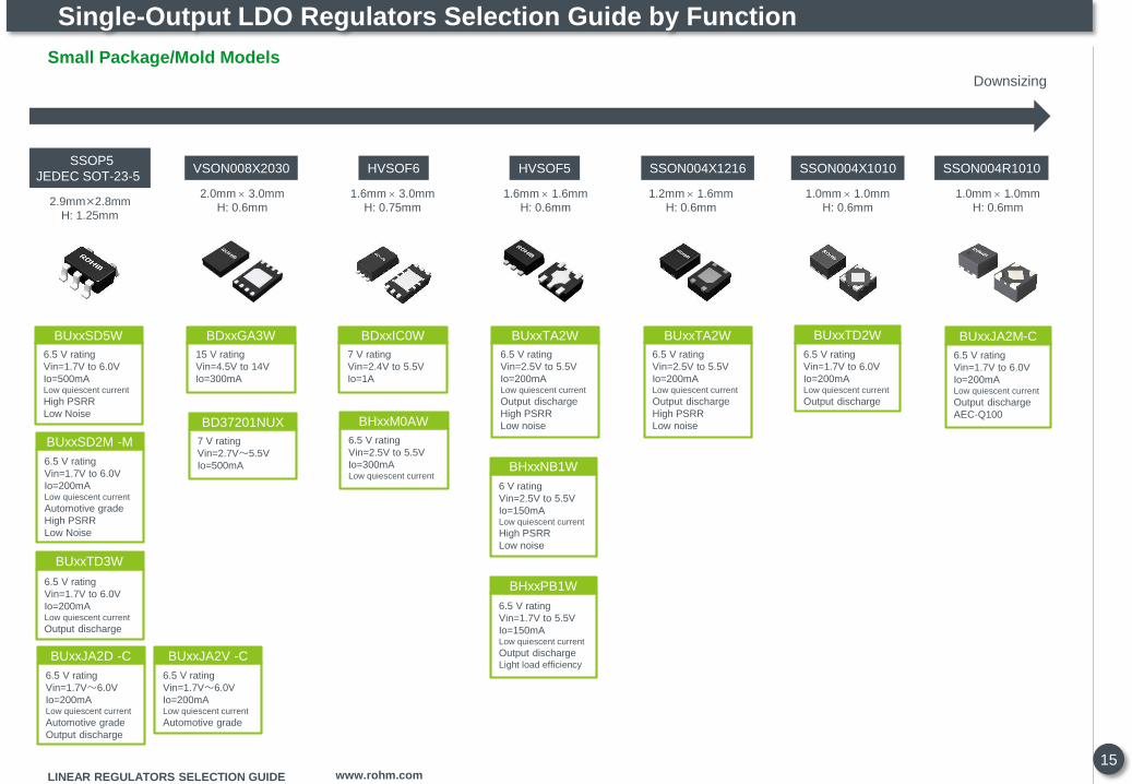
Single-Output LDO Regulators Selection Guide by Function
6.5 V rating
Vin=1.7V to 6.0V
Io=200mALow quiescent current
Automotive grade
High PSRR
Low Noise
6.5 V rating
Vin=1.7V to 6.0V
Io=200mALow quiescent current
Output discharge
15 V rating
Vin=4.5V to 14V
Io=300mA
7 V rating
Vin=2.4V to 5.5V
Io=1A
6.5 V rating
Vin=2.5V to 5.5V
Io=200mALow quiescent current
Output discharge
High PSRR
Low noise
6.5 V rating
Vin=2.5V to 5.5V
Io=200mALow quiescent current
Output discharge
High PSRR
Low noise
VSON008X2030 HVSOF6
6.5 V rating
Vin=2.5V to 5.5V
Io=300mALow quiescent current
HVSOF5
6 V rating
Vin=2.5V to 5.5V
Io=150mALow quiescent current
High PSRR
Low noise
6.5 V rating
Vin=1.7V to 5.5V
Io=150mALow quiescent current
Output dischargeLight load efficiency
SSON004X1216 SSON004X1010
6.5 V rating
Vin=1.7V to 6.0V
Io=200mALow quiescent current
Output discharge
2.0mm 3.0mm
H: 0.6mm
1.6mm 3.0mm
H: 0.75mm
1.6mm 1.6mm
H: 0.6mm
1.2mm 1.6mm
H: 0.6mm
1.0mm 1.0mm
H: 0.6mm
Downsizing
6.5 V rating
Vin=1.7V to 6.0V
Io=500mALow quiescent current
High PSRR
Low Noise
6.5 V rating
Vin=1.7V to 6.0V
Io=200mALow quiescent current
Output discharge
AEC-Q100
SSON004R1010
1.0mm 1.0mm
H: 0.6mm
Small Package/Mold Models
BUxxSD2M -M
BUxxTD3W
BDxxGA3W BDxxIC0W BUxxTA2W BUxxTA2W
BHxxM0AW
BHxxNB1W
BHxxPB1W
BUxxTD2WBUxxSD5W BUxxJA2M-C
2.9mm×2.8mm
H: 1.25mm
SSOP5
JEDEC SOT-23-5
7 V rating
Vin=2.7V~5.5V
Io=500mA
BD37201NUX
6.5 V rating
Vin=1.7V~6.0V
Io=200mALow quiescent current
Automotive grade
Output discharge
BUxxJA2D -C
6.5 V rating
Vin=1.7V~6.0V
Io=200mALow quiescent current
Automotive grade
BUxxJA2V -C

LINEAR REGULATORS SELECTION GUIDE www.rohm.com
16
Single-Output LDO Regulators Selection Guide by Function
6.5 V rating
Vin=2.5V to 5.5V
Io=150mALow quiescent current
VCSP60N1 VCSP60N1
6.5 V rating
Vin=2.2V to 5.5V
Io=150mALow quiescent current
High PSRRHigh-speed response
UCSP50L1
6.5 V rating
Vin=1.7V to 5.5V
Io=200mALow quiescent current
High PSRR
Low noise
UCSP30L1
5.5 V rating
Vin=1.8V to 5.0V
Io=500mALow quiescent current
High PSRR
Low noise
1.0mm 1.04mm
H: 0.6mm, Pitch 0.5mm
0.96mm 0.96mm
H: 0.6mm, Pitch 0.5mm
0.8mm 0.8mm
H: 0.5mm, Pitch 0.4mm
0.8mm 0.8mm
H: 0.33mm, Pitch 0.4mm
Downsizing
Small Package/CSP Models
BHxxRB1W BHxxSA3W BUxxSA4W BUxxSA5W

LINEAR REGULATORS SELECTION GUIDE www.rohm.com
17
Single-Output LDO Regulators Selection Guide by Function
Low Dropout Voltage
Typ MaxIO
Condition
BD3509MUV 112 200 4A 6 4.0 0.7~(VCC−1)
BD3552HFN 200 300 2A 6 2.0 0.95~(VCC−1)
BD3508MUV 65 100 1A 6 3.0 0.75~(VCC−1)
BD3512MUV 65 100 1A 6 3.0 0.7~(VCC−1)
BD3506F 120 200 1A 7 2.5 1.2~(VCC−1)
BD00JC0MNUX -M 200 300 1A 6 1.0 0.95~(VCC−1)
BD3551HFN 200 300 1A 6 1.0 0.95~(VCC−1)
BD3541NUV 200 300 1A 6 1.0 0.95~(VCC−1)
BD3507HFV 165 303 550mA 6 0.55 1.2~(VCC−1)
BD3550HFN 200 300 500mA 6 0.5 0.95~(VCC−1)
BD3540NUV 200 300 500mA 6 0.5 0.95~(VCC−1)
Ultra LDO Type (Two Power Source System)
Part No.
Input
Rating
(V)
Output
Current
(A)
Input Voltage
Range
(V)
Dropout Voltage (mV)
Typ MaxIO
Condition
BD4xxM5 -C 200 500 300mA 45 0.5 4.0~42
BD42754 -C 250 500 300mA 45 0.5 5.5~45
BD357xY -M 250 480 200mA 50 0.5 4.5~36
BD7xxL5 -C 250 500 200mA 50 0.5 4.17~45
BD3020HFP 300 600 200mA 50 0.5 5.6~36
BD3021HFP 300 600 200mA 50 0.5 5.6~36
BD7xxL2 -C 400 700 200mA 50 0.2 4.37~45
BD3010AFV 250 500 150mA 50 0.2 5.6~36
BD4xxM2 -C 160 350 100mA 45 0.2 3.9~42
BD4269 250 500 100mA 45 0.3 6.0~45
45V-50V Rating
Part No.
Input
Rating
(V)
Output
Current
(A)
Input Voltage
Range
(V)
Dropout Voltage (mV)
Typ MaxIO
Condition
BAxxDD0 300 500 1A 35 2.0 3.0~25
BDxxFD0 400 550 1A 35 2.0 4.0~32
BD00D0AW 400 550 1A 35 2.0 4.0~25
BDxxHC5W 360 560 900mA 10 1.5 4.5~8.0
BDxxIC0W 200 300 500mA 7 1.0 2.4~5.5
BDxxFC0 300 500 500mA 35 1.0 4.0~26.5
BAXXCC0 300 500 500mA 35 1.0 4.0~25
BDxxC0A 300 500 500mA 35 1.0VO+1.0
~26.5
BAxxJC5 300 500 500mA 18 1.5 3.0~16
BAxxBC0 300 500 500mA 18 1.0 3.0~16
BDxxGC0W 300 460 500mA 15 1.0 4.5~14
BDxxHC0W 300 460 500mA 10 1.0 4.5~8.0
BD37201NUX 200 500 500mA 7 0.5 2.7~5.5
BDxxGA5W 360 540 300mA 15 0.5 4.5~14
BDxxHA5W 360 540 300mA 10 0.5 4.5~8.0
BDxxIA5W 200 300 250mA 7 0.5 2.4~5.5
BDxxKA5 120 200 200mA 7 0.5 2.3~5.5
BD3650 -M 200 400 200mA 36 0.3 5.6~30
BDxxGA3W 300 600 200mA 15 0.3 4.5~14
BDxxHA3W 400 600 200mA 10 0.3 4.5~8.0
7V-36V Rating
Part No.
Input
Rating
(V)
Output
Current
(A)
Input Voltage
Range
(V)
Dropout Voltage (mV)
Typ MaxIO
Condition
BHxxM0AW 60 90 100mA 6.5 0.3 2.5~5.5
BUxxSA5W 80 150 100mA 5.5 0.5 1.8~5.0
BUxxSA4W 80 150 100mA 6.5 0.2 1.7~5.5
BUxxSD5W 85 150 100mA 6.5 0.5 1.7~6.0
BUxxSD2M -M 85 150 100mA 6.5 0.2 1.7~6.0
BUxxJA2D -C
BUxxJA2V -C85 155 100mA 6.5 0.2 1.7~6.0
BHxxRB1W 100 150 100mA 6.5 0.15 2.5~5.5
BHxxSA3W 100 150 100mA 6.5 0.15 2.2~5.5
BUxxTD2W 110 210 100mA 6.5 0.2 1.7~6.0
BUxxTD3W 110 210 100mA 6.5 0.2 1.7~6.0
BUxxJA2M-C 110 245 100mA 6.5 0.2 1.7~6.0
BUxxTA2W 150 300 100mA 6.5 0.2 2.5~5.5
BHxxPB1W 210 400 100mA 6.5 0.15 1.7~5.5
BHxxNB1W 250 450 100mA 6 0.15 2.5~5.5
6V-6.5V Rating
Part No.
Input
Rating
(V)
Output
Current
(A)
Input Voltage
Range
(V)
Dropout Voltage (mV)
LINEAR REGULATORS SELECTION GUIDE www.rohm.com
18
Single-Output LDO Regulators Selection Guide by Function
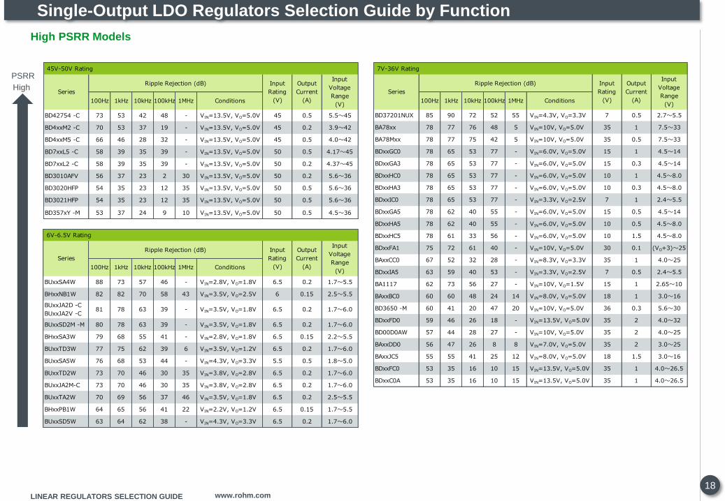
PSRR
High
High PSRR Models
100Hz 1kHz 10kHz 100kHz 1MHz Conditions
BUxxSA4W 88 73 57 46 - VIN=2.8V, VO=1.8V 6.5 0.2 1.7~5.5
BHxxNB1W 82 82 70 58 43 VIN=3.5V, VO=2.5V 6 0.15 2.5~5.5
BUxxJA2D -C
BUxxJA2V -C81 78 63 39 - VIN=3.5V, VO=1.8V 6.5 0.2 1.7~6.0
BUxxSD2M -M 80 78 63 39 - VIN=3.5V, VO=1.8V 6.5 0.2 1.7~6.0
BHxxSA3W 79 68 55 41 - VIN=2.8V, VO=1.8V 6.5 0.15 2.2~5.5
BUxxTD3W 77 75 62 39 6 VIN=3.5V, VO=1.2V 6.5 0.2 1.7~6.0
BUxxSA5W 76 68 53 44 - VIN=4.3V, VO=3.3V 5.5 0.5 1.8~5.0
BUxxTD2W 73 70 46 30 35 VIN=3.8V, VO=2.8V 6.5 0.2 1.7~6.0
BUxxJA2M-C 73 70 46 30 35 VIN=3.8V, VO=2.8V 6.5 0.2 1.7~6.0
BUxxTA2W 70 69 56 37 46 VIN=3.5V, VO=1.8V 6.5 0.2 2.5~5.5
BHxxPB1W 64 65 56 41 22 VIN=2.2V, VO=1.2V 6.5 0.15 1.7~5.5
BUxxSD5W 63 64 62 38 - VIN=4.3V, VO=3.3V 6.5 0.2 1.7~6.0
6V-6.5V Rating
Series
Ripple Rejection (dB) Input
Rating
(V)
Output
Current
(A)
Input
Voltage
Range
(V)
100Hz 1kHz 10kHz 100kHz 1MHz Conditions
BD37201NUX 85 90 72 52 55 VIN=4.3V, VO=3.3V 7 0.5 2.7~5.5
BA78xx 78 77 76 48 5 VIN=10V, VO=5.0V 35 1 7.5~33
BA78Mxx 78 77 75 42 5 VIN=10V, VO=5.0V 35 0.5 7.5~33
BDxxGC0 78 65 53 77 - VIN=6.0V, VO=5.0V 15 1 4.5~14
BDxxGA3 78 65 53 77 - VIN=6.0V, VO=5.0V 15 0.3 4.5~14
BDxxHC0 78 65 53 77 - VIN=6.0V, VO=5.0V 10 1 4.5~8.0
BDxxHA3 78 65 53 77 - VIN=6.0V, VO=5.0V 10 0.3 4.5~8.0
BDxxIC0 78 65 53 77 - VIN=3.3V, VO=2.5V 7 1 2.4~5.5
BDxxGA5 78 62 40 55 - VIN=6.0V, VO=5.0V 15 0.5 4.5~14
BDxxHA5 78 62 40 55 - VIN=6.0V, VO=5.0V 10 0.5 4.5~8.0
BDxxHC5 78 61 33 56 - VIN=6.0V, VO=5.0V 10 1.5 4.5~8.0
BDxxFA1 75 72 61 40 - VIN=10V, VO=5.0V 30 0.1 (VO+3)~25
BAxxCC0 67 52 32 28 - VIN=8.3V, VO=3.3V 35 1 4.0~25
BDxxIA5 63 59 40 53 - VIN=3.3V, VO=2.5V 7 0.5 2.4~5.5
BA1117 62 73 56 27 - VIN=10V, VO=1.5V 15 1 2.65~10
BAxxBC0 60 60 48 24 14 VIN=8.0V, VO=5.0V 18 1 3.0~16
BD3650 -M 60 41 20 47 20 VIN=10V, VO=5.0V 36 0.3 5.6~30
BDxxFD0 59 46 26 18 - VIN=13.5V, VO=5.0V 35 2 4.0~32
BD00D0AW 57 44 28 27 - VIN=10V, VO=5.0V 35 2 4.0~25
BAxxDD0 56 47 26 8 8 VIN=7.0V, VO=5.0V 35 2 3.0~25
BAxxJC5 55 55 41 25 12 VIN=8.0V, VO=5.0V 18 1.5 3.0~16
BDxxFC0 53 35 16 10 15 VIN=13.5V, VO=5.0V 35 1 4.0~26.5
BDxxC0A 53 35 16 10 15 VIN=13.5V, VO=5.0V 35 1 4.0~26.5
7V-36V Rating
Series
Ripple Rejection (dB) Input
Rating
(V)
Output
Current
(A)
Input
Voltage
Range
(V)100Hz 1kHz 10kHz 100kHz 1MHz Conditions
BD42754 -C 73 53 42 48 - VIN=13.5V, VO=5.0V 45 0.5 5.5~45
BD4xxM2 -C 70 53 37 19 - VIN=13.5V, VO=5.0V 45 0.2 3.9~42
BD4xxM5 -C 66 46 28 32 - VIN=13.5V, VO=5.0V 45 0.5 4.0~42
BD7xxL5 -C 58 39 35 39 - VIN=13.5V, VO=5.0V 50 0.5 4.17~45
BD7xxL2 -C 58 39 35 39 - VIN=13.5V, VO=5.0V 50 0.2 4.37~45
BD3010AFV 56 37 23 2 30 VIN=13.5V, VO=5.0V 50 0.2 5.6~36
BD3020HFP 54 35 23 12 35 VIN=13.5V, VO=5.0V 50 0.5 5.6~36
BD3021HFP 54 35 23 12 35 VIN=13.5V, VO=5.0V 50 0.5 5.6~36
BD357xY -M 53 37 24 9 10 VIN=13.5V, VO=5.0V 50 0.5 4.5~36
45V-50V Rating
Series
Ripple Rejection (dB) Input
Rating
(V)
Output
Current
(A)
Input
Voltage
Range
(V)

LINEAR REGULATORS SELECTION GUIDE www.rohm.com
19
Single-Output LDO Regulators Selection Guide by Function
Noise
Low
Low Noise Models
Noise Voltage (μVrms)
10Hz 100Hz 1kHz 10kHz 100kHz BW=10Hz~100kHz
0.62 0.055 0.022 0.014 0.013 4.7 VO = 1.0V
1.8 0.12 0.028 0.014 0.014 6.8 VO = 3.3V
3.2 0.84 0.28 0.15 0.050 30 VO = 1.8V
5.4 1.3 0.62 0.12 0.046 - VO = 3.3V
BUxxSA5W 5.3 1.3 0.52 0.22 0.044 - VO = 3.3V 5.5 0.5 1.8~5.0
- 0.65 0.36 0.22 0.10 - VO = 1.8V
- 1.68 0.62 0.34 0.08 - VO = 3.3V
2.6 0.9 0.32 0.19 0.059 30 VO = 1.8V
5.3 2.4 0.6 0.21 0.045 40 VO = 3.3V
BHxxNB1W - - 1.1 0.34 0.051 75 VO = 2.8V 6 0.15 2.5~5.5
BUxxSD2M -M 6.5 0.2 1.7~6.0
BUxxSD5W 5.3 2.4 0.6 0.21 0.045 40 VO = 3.3V 6.5 0.2 1.7~6.0
BUxxSA4W 6.5 0.2 1.7~5.5
BUxxTA2W 6.5 0.2 2.5~5.5
BD37201NUX 7 0.5 2.7~5.5
Series
Noise Input
Rating
(V)
Output
Current
(A)
Input Voltage
Range
(V)
Output Noise Density (μV/√Hz)Conditions

LINEAR REGULATORS SELECTION GUIDE www.rohm.com
20
Single-Output LDO Regulators Selection Guide by Function
Quiescent
Current
Low
Low Quiescent Current Models
BD7xxL5 -C 6 500 BD4xxM5 -C 38 500 BHxxPB1W 2 150
BD7xxL2 -C 6 200 BD4xxM5W -C 38 500 BUxxSA5W 33 500
BD357xY -M 30 500 BD4xxM2 -C 40 200BUxxJA2D -C
BUxxJA2V -C33 200
BD3020HFP 80 500 BD4xxM2W -C 40 200 BUxxSD5W 33 200
BD3021HFP 80 500BD4269EFJ -M
BD4269FJ -M70
300
200BUxxSD2M -M 33 200
BD3010AFV 80 200 BD4271HFP -C 75 550 BHxxRB1W 34 150
BD42754 -C 75 500 BUxxJA2M-C 35 200
BUxxTD2W 35 200
BUxxTD3W 35 200
BUxxTA2W 40 200
BUxxSA4W 40 200
BHxxSA3W 40 150
BHxxNB1W 60 150
BHxxM0AW 65 300
Circuit
Current
(μA)
Output
Current
(mA)
50V Rating 45V Rating 6V, 6.5V Rating
Series
Circuit
Current
(μA)
Output
Current
(mA)
Series
Circuit
Current
(μA)
Output
Current
(mA)
Series

21LINEAR REGULATORS SELECTION GUIDE www.rohm.com
Multi-Output LDO Regulators
1.2
1.5
1.8
2.6
2.7
2.8
2.9
2.9
5
3.0
3.0
5
3.1
3.2
3.3
CH1 0.6 4.1~16 - ✔ ±2 -
CH2 0.6 2.8~Vcc1 0.8~3.3 ±2 0.8
CH1 1.0 - ✔ ±2 -
CH2 1.0 0.8~3.3 ±2 0.8
CH1 0.5 - ✔ ±2 -
CH2 0.5 - ✔ ±2 -
CH1 0.5 - ✔ ±2 -
CH2 0.5 - ✔ ±2 -
CH1 0.3 - ✔ ✔ ✔ ✔ ✔ ±1.8 -
CH2 0.3 - ✔ ✔ ✔ ✔ ±1.8 -
CH1 0.3 - ✔ ✔ ✔ ✔ ✔ ±1.8 -
CH2 0.3 - ✔ ✔ ✔ ✔ ±1.8 -
CH1 0.1 - ✔ ±2 -
CH2 0.15 2.8~3.3 ✔ ✔ ✔ ✔ ✔ ✔ ✔ ✔ ±2 -
CH1 0.2 - ✔ ±1 -
CH2 0.2 - ✔ ±1 -
CH2 0.2 - ✔ ±25mV -
CH1 0.2 - ✔ ±1 -
CH2 0.2 - ✔ ±25mV -
CH2 0.2 - ✔ ±25mV -
CH1 0.2 - ✔ ±1 -
CH2 0.2 - ✔ ±1 -
CH2 0.2 - ✔ ±25mV -
CH1 0.2 - ✔ ±1 -
CH2 0.2 - ✔ ±25mV -
CH2 0.2 - ✔ ±25mV -
CH1 0.2 - ✔ ±1 -
CH2 0.2 - ✔ ±25mV -
CH2 0.2 - ✔ ±25mV -
CH1 0.2 - ✔ ±1 -
CH2 0.2 - ✔ ±1 -
CH2 0.2 - ✔ ±25mV -
✔ - -✔ ✔ ✔ - ✔ ✔BU6655NUX 3 6 2.5~5.5 120μA
- -40~+85 VSON008X2030BU6654NUX 3 6 2.5~5.5 120μA
- -40~+85 VSON008X2030
✔ - -✔ ✔ ✔ - ✔ ✔
✔ - -✔ ✔ ✔ - ✔ ✔BU6653NUX 3 6 2.5~5.5 120μA
- -40~+85 VSON008X2030BU6652NUX 3 6 2.5~5.5 120μA
- -40~+85 VSON008X2030
✔ - -✔ ✔ ✔ - ✔ ✔
✔ - -✔ ✔ ✔ - ✔ ✔BU6651NUX 3 6 2.5~5.5 120μA
- -40~+85 VSON008X2030BU6650NUX 3 6 2.5~5.5 120μA
- -40~+85 VSON008X2030
✔ - -✔ ✔ ✔ - ✔ ✔
✔ - -✔ ✔ ✔ ✔ - ✔BD7602GUL 2 72.7~5.5
1.7V~3.5V10μA
Programmable
Output-40~+85 VSON008X2020BD7004NUX 2 7 2.5~5.5 55μA
I2C Control
GPO-35~+85
VCSP50L1C
(1.6×1.6×0.57)
✔ - -✔ ✔ ✔ ✔ ✔ ✔
✔ - -✔ ✔ ✔ ✔ ✔ ✔BD7003NUX 2 7 2.5~5.5 55μA
- -25~+105 HRP5BA33D18HFP 2 18 4.1~16 0.7mA
Programmable
Output-40~+85 VSON008X2020
✔ - -- ✔ - - ✔ ✔
HRP5 ✔ - -- ✔ - - ✔ ✔
- 0~+85- - ✔
BA33D15HFP 2 18 4.1~16 0.7mA - -25~+105
Grade
Over
Curr
ent
Pro
tect
ion
Therm
al
Pro
tect
ion
- -
BA3259HFP 2 15 4.75~14 3mA - ✔
✔ ✔ - -25~+105 HRP7 ✔
HRP5 ✔ - -✔
BA30E00WHFP 2 18 0.7mA ✔ - - -
Consu
mer
Indust
rial
Part No. Outputs
Input
Voltage
Maximum
Rating
(V)
CH
Output
Current
(A)
Input
Voltage
Range
(V)
Output Voltage (V)
Output
Voltage
Accuracy
(%)
Vref
(V)
Auto
motive
Adju
stable
Fixed
Enable
Cera
mic
Capaci
tor
Outp
ut
Dis
charg
e
UVLO
Circuit
Current
Features
Other
Features
Operating
Temperature
(°C)
Package
(mm)

22LINEAR REGULATORS SELECTION GUIDE www.rohm.com
LDO+ (Plus)
The lineup includes the BD4269FJ, BD4269EFJ and BD4275
that integrate a voltage detector function. These models are
useful for monitoring for abnormal voltages. The lineup includes
the BD4271, BD3010AFV, BD3020HFP and BD3021HFP that
integrate a watchdog timer/voltage detector circuit. These
models are useful for monitoring for malfunctions and abnormal
voltages of microcontrollers.
200 mA output
I/O voltage detector
Large current
300 mA output
I/O voltage detector
Large current
500 mA output
Output voltage detector
45 V rating
200 mA output
Watchdog timer
Voltage detector
Detection voltage
variable
Large current
500 mA output
Watchdog timer
WDT OFF control
Voltage detector
Detection voltage
variable
WDT OFF
control500 mA output
Watchdog timer
Voltage detector
Detection voltage
variable
WDT: Watchdog timer
BD4269FJ -C
BD4269EFJ -C
BD42754 -CBD3020HFP
BD3010AFV
BD3021HFP
50 V rating
550 mA output
Watchdog timerOutput voltage detector
Enable
BD4271 -C
Large current
WDT
Enable
System Diagram
Automotive grade Tolerance of 2% across the
entire temperature range
Low quiescent
current models
Output ceramic capacitor-
supported models
1.2
1.5
1.8
2.5
3.0
3.3
5.0
6.0
7.0
8.0
9.0
10
12
BD3020HFP 50 0.5 5.6~36 - ✔ ±2*1 - 80μA - ✔ ✔
Adjust
able✔ ✔ -40~+125 HRP7 - - ✔
BD3021HFP 50 0.5 5.6~36 - ✔ ±2*1 - 80μA - ✔ ✔ Fixed ✔ ✔ WDT OFF control -40~+125 HRP7 - - ✔
BD3010AFV 50 0.2 5.6~36 - ✔ ±2*1 - 80μA - ✔ ✔
Adjust
able✔ ✔ -40~+125 SSOP-B20 - - ✔
BD4271HFP -C
BD4271FP2 -C45 0.55 6.0~45 - ✔ ±2
*1 - 75μA ✔ ✔ ✔ Fixed ✔ ✔ AEC-Q100Tj
-40~+150
HRP7
TO263-7- - ✔
BD42754 -C 45 0.5 5.5~45 - ✔ ±2*1 - 75μA - ✔ - Fixed ✔ ✔ AEC-Q100Tj
-40~+150
TO252-J5
TO263-5- - ✔
BD4269EFJ -C
BD4269FJ -C45
0.3
0.26.0~45 - ✔ ±2
*1 - 70μA - ✔ - Adjustable ✔ ✔ AEC-Q100Tj
-40~+150
HTSOP-J8
SOP-J8- - ✔
Consu
mer
Indust
rial
Auto
motive
Voltage D
ete
ctor
*1:Accuracy over temperature WDT: Watchdog Timer
Other
Features
Operating
Temperature
(°C)
Package
Over
Curr
ent
Pro
tect
ion
Therm
al
Pro
tect
ion
Series
Input
Voltage
Maximum
Rating
(V)
Output
Current
(A)
Input
Voltage
Range
(V)
Output Voltage (V)
Output
Voltage
Accuracy
(%)
Vref
(V)
Circuit
Current
Features Grade
Adju
stable
Fixed
Enable
Cera
mic
Capaci
tor
Watc
hdog T
imer

23LINEAR REGULATORS SELECTION GUIDE www.rohm.com
Microcontroller Monitoring Power Supply Solutions
Product example: BD3010AFV, BD3020HFP, BD3021HFP
Ultra-low quiescent current: 80µA (Typ)
Output transistor: Pch DMOS low saturated type
Maximum rated voltage: 50V
Output current: 200mA , 500mA
Output voltage: 5.0V 2%
(Across the entire temperature range)
A low ESR ceramic capacitor is available for output phase compensation.
The built-in watchdog timer monitors for microcontroller hang-ups and
resets the microcontroller in the event thereof, which enables the system
to restart automatically.
The watchdog timer is automatically turned ON/OFF depending on the
load current so as to avoid unnecessary monitoring by the timer when the
microcontroller is in the sleep mode (BD3010).
Forced ON/OFF control enables the watchdog timer to stay OFF until the
system is stable, e.g., when the microcontroller (BD3010, BD3021) starts
up, etc.
The built-in undervoltage output reset (power-on reset) circuit enables
setting of the actuation delay time.
The reset detection voltage is adjustable (BD3010, BD3020).
The built-in output current control circuit prevents damage to the IC by
output short-circuiting.
The built-in thermal shutdown circuit prevents thermal damage to the IC if
overloaded.
The BD3010AFV, BD3020HFP and BD3021HFP are regulators with a rated voltage of 50 V and output current of 200 mA/500 mA. They are power supply ICs that integrate a watchdog
timer (WDT) that monitors for microcontroller malfunctions and a reset circuit that monitors power supply voltage on a single chip.
Function BD3010 BD3020 BD3021
WDT
WDT auto ON/OFF - -
WDT forced ON/OFF -
Reset detection voltage Variable Variable Fixed
Battery VCC
RADJ
OUT
WADJ
CLK
INH
ROCT GND
WDT Enable
Reset
VDD
CLKOUT
PIO
RESET
5V, 200mA12V
OUT
VC
C
OUT
RADJ
WADJ
CLK
INH
RO
BD3010AFV
GNDCT
Microcontroller
VDD
CLKOUT
PIO
RESE
T
Battery VCC
VS
VOUT
CLK
RESETCT GNDReset
VDD
CLKOUT
RESET
5V, 500mA12V
VOUTBattery VC
C
VOUT
VS
CLK
RESE
T
BD3020HFP
GNDCT
Microcontroller
VDD
CLKOUT
RESE
T
Battery VCC VOUT
CLK
INH
RESETCT GND
WDT Enable
Reset
VDD
CLKOUT
PIO
RESET
5V, 500mA12VBattery VC
C
VOUT
CLK
INH
RESE
T
BD3021HFP
GNDCT
Microcontroller
VDD
CLKOUT
PIO
RESE
T
Battery
LDO+ (Plus)

24LINEAR REGULATORS SELECTION GUIDE www.rohm.com
Power Supply Monitoring Solutions
Product example: BD4269FJ-C, BD4269EFJ-C,
BD42754FP2-C, BD42754FPJ-C
Ultra-low quiescent current: 70µA (BD4269) , 65μA (BD4275)
Output transistor: Pch DMOS low saturated type
Maximum rated voltage: 45V
Output current: 200mA (BD4269FJ) , 300mA (BD4269EFJ), 500mA (BD42754)
Output voltage: 5.0V 2% (Across the entire temperature range)
A low ESR ceramic capacitor is available for output capacitor.
The built-in undervoltage output reset (power-on reset) circuit enables setting of the
actuation delay time.
The power voltage detection reset circuit is built in, which enables monitoring of input power
voltage or other power voltages (BD4269).
The detection voltage for the output low voltage reset circuit and power voltage detection
reset circuit (BD4269) can be adjusted with an external resistor.
The built-in output current control circuit prevents damage to the IC by output short-circuiting.
The built-in thermal shutdown circuit prevents thermal damage to the IC if overloaded.
BD4269FJ-C, BD4269EFJ-C, BD42754FP2-C and BD42754FPJ-C regulators have a rated voltage of 45 V and output current of 200 mA to 500 mA. They are power supply ICs that integrate
a reset circuit for monitoring power supply voltage on a single chip.
Timing Chart
BD4269FJ-C
Io=200mA
BD4269EFJ-C
Io=300mA
BD42754FP2-C
Io=500mA
BD42754FPJ-C
Io=500mA
SOP-J8 HTSOP-J8 TO263-5 TO252-J5
Battery VCC
SI
VO
SO
CT GND
ResetVDD
RESET
5V, 200mA/300mA12V
RO
RADJ
Battery VC
C
VO
SI
SO
RO
RADJ
BD4269FJ-C
BD4269EFJ-C
GNDCT
Microcontroller
VDD
RESE
T
Microcontroller
Battery VCC VO
CT GNDReset
VDD
RESET
5V, 500mA12V
RO
VC
C
VO
RO
BD42754FP2-C
BD42754FPJ-C
GNDCT
Battery VDD
RESE
T
LDO+ (Plus)

25LINEAR REGULATORS SELECTION GUIDE www.rohm.com
Support of JEDEC DDR1/2/3/3L
Product example: BD35395FJ-M
The BD35395FJ-M is a terminal regulator that
supports DDR1/2/3/3L SDRAMs in conformity with
JEDEC. It integrates a VTT power supply, one of the
three power supplies required for the DDR memory.
VTT output is a linear power supply that integrates
an N-MOSFET and is capable of supplying a
maximum 1 A both to the sink and source. The
internal OP-AMP designed for high-speed operation
helps realize excellent transient response
characteristics. To drive the internal N-MOSFET, a
bias power supply of 3.3 V or 5.0 V is required. This
linear regulator possesses an independent standard
input pin (VDDQ) and an independent feedback pin
(VTTS) in order to keep the JEDEC-specified voltage
precision, and contribute to excellent output voltage
precision and load regulation.BD35395FJ-M Application Circuit
DDR SDRAM Power Supply Solutions
3.3V to 5.0VBD9B300MUV
BD9B600MUV
Controller
1.5V
DDR3L SDRAM
BD35395FJ-M
VDDQ
VTT
VTT_INVCC
VREF…
VDDQ VDDQ
VDDQ
VTT
RT
A DDR memory needs three power supplies. For
VDDQ, a power supply to drive the memory cell, high-
speed load response and voltage precision are
required in order to assure reliability in memory
operations. Input to the memory cell is judged based
on VREF, which is one-half of VDDQ voltage.
Although the required current value is small, voltage
precision is required in response to changes in VDDQ
voltage. VTT is the termination voltage of the memory
output, which terminates the memory output via a
terminal resistor RT. Its voltage is one-half of VDDQ
and is required to follow changes in VDDQ voltage like
VREF. As the memory output switches to High or Low,
the output current must be capable of following the
source or sink operation at a high speed.
Input voltage range: 2.7V to 5.5V
Output current: 1A
DDR1/2/3/3L SDRA supported
A push/pull power supply for termination is built in (VTT).
Ceramic capacitor supported for output
Enable function
Power good output with settable delay
Built-in thermal shutdown circuit (TSD)
Built-in undervoltage lockout circuit (UVLO)
Termination Regulators for DDR SDRAM

26LINEAR REGULATORS SELECTION GUIDE www.rohm.com
Termination Regulators for DDR SDRAM
DD
R1 (
2.5
V/2
.6V)
DD
R2 (
1.8
V)
DD
R2L (
1.5
V)
LPD
DR2 (
1.2
V)
DD
R3 (
1.5
V)
DD
R3L (
1.3
5V)
DD
R3U
(1.2
5V)
LPD
DR3 (
1.2
V)
DD
R4 (
1.2
V)
BD3533F
BD3533FVM
BD3533HFN
2.7 to 5.5 1.0 to 5.5 1.0 to 2.75 0.75 to 1.25 ±30 ±1.0 ±20 ✔ ✔ - ✔ - Recovery ✔ ✔ - - - - - - - -20 to +100
SOP8
MSOP8
HSON8
BD3539FVM
BD3539NUX2.7 to 5.5 1.0 to 5.5 1.0 to 2.75 0.75 to 1.25 ±15 ±1.0 ±25 ✔ ✔ - ✔ ✔ Recovery ✔ ✔ ✔ - ✔ - - - - -30 to +100
MSOP8
VSON008X2030
BD35390FJ 2.7 to 5.5 1.0 to 5.5 1.0 to 2.75 0.75 to 1.25 ±15 ±1.0 - ✔ ✔ ✔ ✔ ✔ Recovery ✔ ✔ ✔ - ✔ - - - - -30 to +100 SOP-J8
BD35395FJ-M 2.7 to 5.5 1.0 to 5.5 1.0 to 2.75 0.5 to 1.375 ±13.5 ±1.0 - ✔ ✔ ✔ ✔ ✔ Recovery ✔ ✔ ✔ - ✔ ✔ - - - -40 to +105 SOP-J8
Enable
Soft
Sta
rt
Pow
er
Good
UVLO
Outp
ut
Cera
mic
Capaci
tors
Therm
al
Pro
tect
ion
DDR (VDDQ)
VTT
Output
Current
(A)
VREF
Output
Current
(mA)
Features
Operating
Temperature
(℃)
Package
VTT
Voltage
Precision
(mV)
Part No.
VCC
Input
Voltage
(V)
VTT_IN
Termination
Input
Voltage
(V)
VDDQ
Reference
Input
Voltage
(V)
VTT
Output
Voltage
(V)
27LINEAR REGULATORS SELECTION GUIDE www.rohm.com
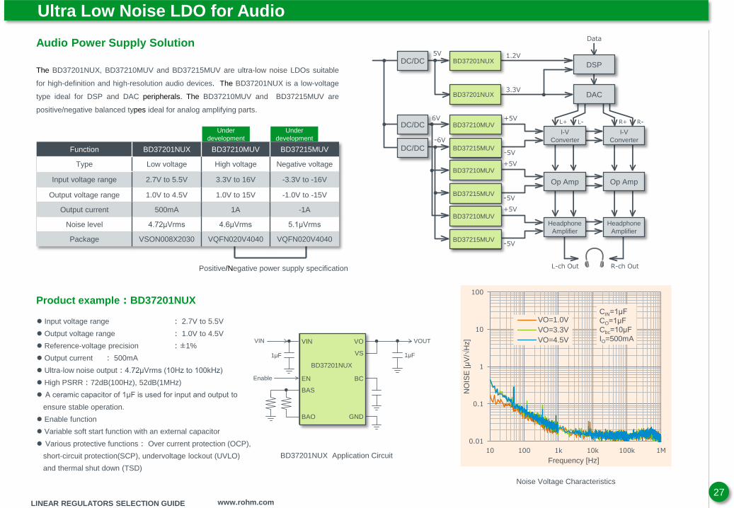
Product example:BD37201NUX
Audio Power Supply Solution
The BD37201NUX, BD37210MUV and BD37215MUV are ultra-low noise LDOs suitable
for high-definition and high-resolution audio devices. The BD37201NUX is a low-voltage
type ideal for DSP and DAC peripherals. The BD37210MUV and BD37215MUV are
positive/negative balanced types ideal for analog amplifying parts.
0.01
0.1
1
10
100
10 100 1k 10k 100k 1M
NO
ISE
[μ
V/√
Hz]
Frequency [Hz]
VO=1.0V
VO=3.3V
VO=4.5V
CIN=1μF
CO=1μF
Cbc=10μF
IO=500mAVIN
Enable
VIN
EN
VO
1μF 1μF
VOUT
BAS
BAO
VS
BC
GND
VIN
BAS
VO
BD37201NUX
EN
BAO
VS
BC
GND
Noise Voltage Characteristics
BD37201NUX Application Circuit
DSP
L+BD37210MUV
HeadphoneAmplifier
DAC
I-VConverter
I-VConverter
Op Amp
HeadphoneAmplifier
Op Amp
L- R+ R-
BD37201NUX
BD37201NUX
BD37215MUV
BD37210MUV
BD37215MUV
1.2V
3.3V
+5V
-5V
Data
L-ch Out R-ch Out
DC/DC
DC/DC
DC/DC
5V
6V
-6V
+5V
-5V
BD37210MUV
BD37215MUV
+5V
-5V
BD37201NUXDC/DC
BD37201NUX
BD37210MUV
BD37215MUV
DC/DC
DC/DC
DSP
DAC
I-V
Converter
I-V
Converter
Op Amp Op Amp
Headphone
Amplifier
Headphone
Amplifier
BD37210MUV
BD37215MUV
BD37210MUV
BD37215MUV
Positive/Negative power supply specification
Input voltage range : 2.7V to 5.5V
Output voltage range : 1.0V to 4.5V
Reference-voltage precision :±1%
Output current : 500mA
Ultra-low noise output:4.72μVrms (10Hz to 100kHz)
High PSRR:72dB(100Hz), 52dB(1MHz)
A ceramic capacitor of 1μF is used for input and output to
ensure stable operation.
Enable function
Variable soft start function with an external capacitor
Various protective functions: Over current protection (OCP),
short-circuit protection(SCP), undervoltage lockout (UVLO)
and thermal shut down (TSD)
Under
development
Under
development
Function BD37201NUX BD37210MUV BD37215MUV
Type Low voltage High voltage Negative voltage
Input voltage range 2.7V to 5.5V 3.3V to 16V -3.3V to -16V
Output voltage range 1.0V to 4.5V 1.0V to 15V -1.0V to -15V
Output current 500mA 1A -1A
Noise level 4.72μVrms 4.6μVrms 5.1μVrms
Package VSON008X2030 VQFN020V4040 VQFN020V4040
Ultra Low Noise LDO for Audio

28LINEAR REGULATORS SELECTION GUIDE www.rohm.com
Ultra Low Noise LDO for Audio
Output
Voltage (V)
☆ BD37210MUV 17.5 1.0 3.0~16 1.0~15 ±1 1.0 T.B.D. ✔ ✔ ✔ - ✔ ✔ -
Ultralow Noise
High PSRR
UVLO
-40~+85 VQFN020V4040 ✔ - -
☆ BD37215MUV -17.5 -1.0 -3.0~-16 -1.0~-15 ±1 -1.0 T.B.D. ✔ ✔ ✔ - ✔ ✔ -
Ultralow Noise
High PSRR
UVLO
-40~+85 VQFN020V4040 ✔ - -
BD37201NUX 7 0.5 2.7~5.5 1.0~4.5 ±1 1.0 1.33mA ✔ ✔ ✔ - ✔ ✔ -
Ultralow Noise
High PSRR
UVLO
-40~+85 VSON008X2030 ✔ - -
☆Under Development
Series
Input
Voltage
Maximum
Rating
(V)
Output
Current
(A)
Input
Voltage
Range
(V)
Output
Voltage
Accuracy
(%)
Vref
(V)
Circuit
Current
Features
Adju
stable
Enable
Cera
mic
Capaci
tor
Soft
Sta
rt
Outp
ut
Dis
charg
e
Indust
rial
Auto
motive
Other
Features
Operating
Temperature
(°C)
Package
Grade
Over
Curr
ent
Pro
tect
ion
Therm
al
Pro
tect
ion
Over
Voltage
Pro
tect
ion
Consu
mer

LINEAR REGULATORS SELECTION GUIDE www.rohm.com
29
Package
Surface-Mounting Packages Surface-Mounting Packages
Type AppearancePackage
Symbol
Size (mm)
W (Typ) × D (Typ) × H (Max)
HTSOP-J8 EFJ 4.90mm × 6.00mm × 1.00mm
SOP-J8 FJ 4.90mm × 6.00mm × 1.65mm
SOP8 F 5.00mm × 6.20mm × 1.71mm
SSOP-B20 FV 6.50mm × 6.40mm × 1.45mm
SSON004X1010 NVX 1.00mm × 1.00mm × 0.60mm
SSON004R1010 NVX 1.00mm × 1.00mm × 0.60mm
SSON004X1216 NVX 1.20mm × 1.60mm × 0.60mm
HVSOF5 HFV 1.60mm × 1.60mm × 0.60mm
HVSOF6 HFV 1.60mm × 3.00mm × 0.75mm
Type AppearancePackage
Symbol
Size (mm)
W (Typ) × D (Typ) × H (Max)
VSON008X2030 NUX 2.00mm × 3.00mm × 0.60mm
VSON010V3030 NUV 3.00mm × 3.00mm × 1.00mm
VSON010X3030 NUX 3.00mm × 3.00mm × 0.60mm
VQFN020V4040 MUV 4.00mm × 4.00mm × 1.00mm
SSOP5
(SOT-23-5)G 2.90mm × 2.80mm × 1.25mm
SOT89-3K FP3 4.50mm × 4.095mm × 1.60mm
SOT223-4F FP3 6.53mm × 7.00mm × 1.80mm
TO252-3 FP 6.50mm × 9.50mm × 2.50mm
TO252S-3 FPS 6.50mm × 9.50mm × 1.30mm
TO252-5 FP 6.50mm x 9.50mm x 2.50mm

LINEAR REGULATORS SELECTION GUIDE www.rohm.com
30
Package
Surface-Mounting Packages Through-hole Packages
Wafer-level Chip-size Packages
Type AppearancePackage
Symbol
Size (mm)
W (Typ) × D (Typ) × H (Max)
TO220CP-3 CP 10.00mm x 20.81mm x 4.60mm
TO220FP-3 T 10.00mm x 30.50mm x 4.60mm
TO220CP-V5 CP 10.00mm x 20.12mm x 4.60mm
TO220FP-5 T 10.00mm x 30.50mm x 4.60mm
Type AppearancePackage
Symbol
Size (mm)
W (Typ) × D (Typ) × H (Max)
VCSP60N1 GUT
UCSP30L1 GWZ
UCSP50L1 GWL
Refer to the data
sheets of the
respective models.
Refer to the data sheets of the
respective models.
Type AppearancePackage
Symbol
Size (mm)
W (Typ) × D (Typ) × H (Max)
TO252-J5(F) FPJ 6.60mm x 10.10mm x 2.38mm
TO263-3(F) FP2 10.16mm x 15.10mm x 4.70mm
TO263-5(F) FP2 10.16mm x 15.10mm x 4.70mm
TO263-7 FP2 10.16mm x 15.10mm x 4.70mm
HRP5 HFP 9.395mm x 10.54mm x 2.005mm
HRP7 HFP 9.395mm x 10.54mm x 2.005mm
AEK60-A1-074 ©2017 ROHM Co., Ltd. Application Engineer Div.
Notes
1. The information contained herein is subject to change without notice.
2. Before you use our Products, please contact our sales representative and verify the latest specifications.
3. Although ROHM is continuously working to improve product reliability and quality, semicon- ductors can
break down and malfunction due to various factors. Therefore, in order to prevent personal injury or fire
arising from failure, please take safety measures such as complying with the derating characteristics,
implementing redundant and fire prevention designs, and utilizing backups and failsafe procedures. ROHM
shall have no responsibility for any damages arising out of the use of our Poducts beyond the rating
specified by ROHM.
4. Examples of application circuits, circuit constants and any other information contained herein are provided
only to illustrate the standard usage and operations of the Products. The peripheral conditions must be
taken into account when designing circuits for mass production.
5. The technical information specified herein is intended only to show the typical functions of and examples
of application circuits for the Products. ROHM does not grant you, explicitly or implicitly, any license to use
or exercise intellectual property or other rights held by ROHM or any other parties. ROHM shall have no
responsibility whatsoever for any dispute arising out of the use of such technical information.
6. The Products are intended for use in general electronic equipment (i.e. AV/OA devices, communication,
consumer systems, gaming/entertainment sets) as well as the applications indicated in this document.
7. The Products specified in this document are not designed to be radiation tolerant.
8. For use of our Products in applications requiring a high degree of reliability (as exemplified below), please
contact and consult with a ROHM representative : transportation equipment (i.e. cars, ships, trains),
primary communication equipment, traffic lights, fire/crime prevention, safety equipment, medical systems,
servers, solar cells, and power transmission systems.
9. Do not use our Products in applications requiring extremely high reliability, such as aerospace equipment,
nuclear power control systems, and submarine repeaters.
10. ROHM shall have no responsibility for any damages or injury arising from non-compliance with the
recommended usage conditions and specifications contained herein.
11. ROHM has used reasonable care to ensure the accuracy of the information contained in this document.
However, ROHM does not warrants that such information is error-free, and ROHM shall have no
responsibility for any damages arising from any inaccuracy or misprint of such information.
12. Please use the Products in accordance with any applicable environmental laws and regulations, such as
the RoHS Directive. For more details, including RoHS compatibility, please contact a ROHM sales office.
ROHM shall have no responsibility for any damages or losses resulting non-compliance with any
applicable laws or regulations.
13. When providing our Products and technologies contained in this document to other countries, you must
abide by the procedures and provisions stipulated in all applicable export laws and regulations, including
without limitation the US Export Administration Regulations and the Foreign Exchange and Foreign Trade
Act.
14. This document, in part or in whole, may not be reprinted or reproduced without prior consent of ROHM.