lifetime improvement of nand flash-based storage … · usenix association 12th usenix conference...
TRANSCRIPT

This paper is included in the Proceedings of the 12th USENIX Conference on File and Storage Technologies (FAST ’14).
February 17–20, 2014 • Santa Clara, CA USA
ISBN 978-1-931971-08-9
Open access to the Proceedings of the 12th USENIX Conference on File and Storage
Technologies (FAST ’14) is sponsored by
Lifetime Improvement of NAND Flash-based Storage Systems Using Dynamic Program
and Erase ScalingJaeyong Jeong and Sangwook Shane Hahn, Seoul National University;
Sungjin Lee, MIT/CSAIL; Jihong Kim, Seoul National University
https://www.usenix.org/conference/fast14/technical-sessions/presentation/jeong

USENIX Association 12th USENIX Conference on File and Storage Technologies 61
Lifetime Improvement of NAND Flash-based Storage SystemsUsing Dynamic Program and Erase Scaling
Jaeyong Jeong∗, Sangwook Shane Hahn∗, Sungjin Lee†, and Jihong Kim∗
∗Dept. of CSE, Seoul National University, {jyjeong, shanehahn, jihong}@davinci.snu.ac.kr†CSAIL, Massachusetts Institute of Technology, [email protected]
AbstractThe cost-per-bit of NAND flash memory has been con-tinuously improved by semiconductor process scalingand multi-leveling technologies (e.g., a 10 nm-node TLCdevice). However, the decreasing lifetime of NANDflash memory as a side effect of recent advanced tech-nologies is regarded as a main barrier for a wide adop-tion of NAND flash-based storage systems. In this paper,we propose a new system-level approach, called dynamicprogram and erase scaling (DPES), for improving thelifetime (particularly, endurance) of NAND flash mem-ory. The DPES approach is based on our key observationthat changing the erase voltage as well as the erase timesignificantly affects the NAND endurance. By slowlyerasing a NAND block with a lower erase voltage, we canimprove the NAND endurance very effectively. By mod-ifying NAND chips to support multiple write and erasemodes with different operation voltages and times, DPESenables a flash software to exploit the new tradeoff rela-tionships between the NAND endurance and erase volt-age/speed under dynamic program and erase scaling. Wehave implemented the first DPES-aware FTL, called aut-oFTL, which improves the NAND endurance with a neg-ligible degradation in the overall write throughput. Ourexperimental results using various I/O traces show thatautoFTL can improve the maximum number of P/E cy-cles by 61.2% over an existing DPES-unaware FTL withless than 2.2% decrease in the overall write throughput.
1 Introduction
NAND flash-based storage devices are increasingly pop-ular from mobile embedded systems (e.g., smartphonesand smartpads) to large-scale high-performance enter-prise servers. Continuing semiconductor process scal-ing (e.g., 10 nm-node process technology) combinedwith various recent advances in flash technology (suchas a TLC device [1] and a 3D NAND device [2]) is ex-pected to further accelerate an improvement of the cost-
per-bit of NAND devices, enabling a wider adoption ofNAND flash-based storage systems. However, the poorendurance of NAND flash memory, which deterioratesfurther as a side effect of recent advanced technologies,is still regarded as a main barrier for sustainable growthin the NAND flash-based storage market. (We representthe NAND endurance by the maximum number of pro-gram/erase (P/E) cycles that a flash memory cell can tol-erate while preserving data integrity.) Even though theNAND density doubles every two years, the storage life-time does not increase as much as expected in a recentdevice technology [3]. For example, the NAND stor-age lifetime was increased by only 20% from 2009 to2011 because the maximum number of P/E cycles wasdecreased by 40% during that period. In particular, inorder for NAND flash memory to be widely adopted inhigh-performance enterprise storage systems, the deteri-orating NAND endurance problem should be adequatelyresolved.
Since the lifetime LC of a NAND flash-based stor-age device with the total capacity C is proportional tothe maximum number MAXP/E of P/E cycles, and is in-versely proportional to the total written data Wday perday, LC (in days) can be expressed as follows (assuminga perfect wear leveling):
LC =MAXP/E ×CWday ×WAF
, (1)
where WAF is a write amplification factor which rep-resents the efficiency of an FTL algorithm. Many ex-isting lifetime-enhancing techniques have mainly fo-cused on reducing WAF by increasing the efficiencyof an FTL algorithm. For example, by avoiding un-necessary data copies during garbage collection, WAFcan be reduced [4]. In order to reduce Wday, vari-ous architectural/system-level techniques were proposed.For example, data de-duplication [5], data compres-sion [6] and write traffic throttling [7] are such exam-ples. On the other hand, few system/software-level tech-niques were proposed for actively increasing the max-

62 12th USENIX Conference on File and Storage Technologies USENIX Association
imum number MAXP/E of P/E cycles. For example, arecent study [8] suggests MAXP/E can be indirectly im-proved by a self-recovery property of a NAND cell butno specific technique was proposed yet.
In this paper, we propose a new approach, called dy-namic program and erase scaling (DPES), which can sig-nificantly improve MAXP/E . The key intuition of our ap-proach, which is motivated by a NAND device physicsmodel on the endurance degradation, is that changingthe erase voltage as well as the erase time significantlyaffects the NAND endurance. For example, slowly eras-ing a NAND block with a lower erase voltage can im-prove the NAND endurance significantly. By modify-ing a NAND device to support multiple write and erasemodes (which have different voltage/speed and differ-ent impacts on the NAND endurance) and allowing afirmware/software module to choose the most appropri-ate write and erase mode (e.g., depending on a givenworkload), DPES can significantly increase MAXP/E .
The physical mechanism of the endurance degradationis closely related to stress-induced damage in the tunneloxide of a NAND memory cell [9]. Since the probabil-ity of stress-induced damage has an exponential depen-dence on the stress voltage [10], reducing the stress volt-age (particularly, the erase voltage) is an effective wayof improving the NAND endurance. Our measurementresults with recent 20 nm-node NAND chips show thatwhen the erase voltage is reduced by 14% during P/E cy-cles, MAXP/E can increase on average by 117%. How-ever, in order to write data to a NAND block erased withthe lower erase voltage (which we call a shallowly erasedblock in the paper), it is necessary to form narrow thresh-old voltage distributions after program operations. Sinceshortening the width of a threshold voltage distributionrequires a fine-grained control during a program opera-tion, the program time is increased if a lower erase volt-age was used for erasing a NAND block.
Furthermore, for a given erase operation, since a nom-inal erase voltage (e.g., 14 V) tends to damage the cellsmore than necessary in the beginning period of an eraseoperation [11], starting with a lower (than the nominal)erase voltage and gradually increasing to the nominalerase voltage can improve the NAND endurance. How-ever, gradually increasing the erase voltage increases theerase time. For example, our measurement results withrecent 20 nm-node NAND chips show that when the ini-tial erase voltage of 10 V is used instead of 14 V duringP/E cycles, MAXP/E can increase on average by 17%. Onthe other hand, the erase time is increased by 300%.
Our DPES approach exploits the above two tradeoffrelationships between the NAND endurance and erasevoltage/speed at the firmware-level (or the software levelin general) so that the NAND endurance is improvedwhile the overall write throughput is not affected. For ex-ample, since the maximum performance of NAND flash
memory is not always needed in real workloads, a DPES-based technique can exploit idle times between consec-utive write requests for shortening the width of thresh-old voltage distributions so that shallowly erased NANDblocks, which were erased by lower erase voltages, canbe used for most write requests. Idle times can be alsoused for slowing down the erase speed. If such idle timescan be automatically estimated by a firmware/systemsoftware, the DPES-based technique can choose the mostappropriate write speed for each write request or selectthe most suitable erase voltage/speed for each erase op-eration. By aggressively selecting endurance-enhancingerase modes (i.e., a slow erase with a lower erase volt-age) when a large idle time is available, the NAND en-durance can be significantly improved because less dam-aging erase operations are more frequently used.
In this paper, we present a novel NAND endurancemodel which accurately captures the tradeoff relation-ship between the NAND endurance and erase volt-age/speed under dynamic program and erase scaling.Based on our NAND endurance model, we have im-plemented the first DPES-aware FTL, called autoFTL,which dynamically adjusts write and erase modes inan automatic fashion, thus improving the NAND en-durance with a negligible degradation in the overallwrite throughput. In autoFTL, we also revised keyFTL software modules (such as garbage collector andwear-leveler) to make them DPES-aware for maximiz-ing the effect of DPES on the NAND endurance. Sinceno NAND chip currently allows an FTL firmware tochange its program and erase voltages/times dynami-cally, we evaluated the effectiveness of autoFTL with theFlashBench emulation environment [12] using a DPES-enabled NAND simulation model (which supports mul-tiple write and erase modes). Our experimental resultsusing various I/O traces show that autoFTL can improveMAXP/E by 61.2% over an existing DPES-unaware FTLwith less than 2.2% decrease in the overall write through-put.
The rest of the paper is organized as follows. Section 2briefly explains the basics of NAND operations relatedto our proposed approach. In Section 3, we present theproposed DPES approach in detail. Section 4 describesour DPES-aware autoFTL. Experimental results followin Section 5, and related work is summarized in Sec-tion 6. Finally, Section 7 concludes with a summary andfuture work.
2 Background
In order to improve the NAND endurance, our proposedDPES approach exploits key reliability and performanceparameters of NAND flash memory during run time. Inthis section, we review the basics of various reliabil-ity parameters and their impact on performance and en-
2

USENIX Association 12th USENIX Conference on File and Storage Technologies 63
MP1 WP1 MP2 WP2 MP3 WP3
11 10 00 01
WVth
VRead
VthMRead
VRef0 VRef1 VRef2
Figure 1: An example of threshold voltage distributionsfor multi-level NAND flash memory and primary relia-bility parameters.
durance of NAND cells.
2.1 Threshold Voltage Distributions ofNAND Flash Memory
Multi-level NAND flash memory stores 2 bits in a cellusing four distinct threshold voltage levels (or states) asshown in Figure 1. Four states are distinguished by dif-ferent reference voltages, VRe f 0, VRe f 1 and VRe f 2. Thethreshold voltage gap MPi between two adjacent statesand the width WPi of a threshold voltage distribution aremainly affected by data retention and program time re-quirements [13, 14], respectively. As a result, the totalwidth WVth of threshold voltage distributions should becarefully designed to meet all the NAND requirements.In order for flash manufacturers to guarantee the reliabil-ity and performance requirements of NAND flash mem-ory throughout its storage lifespan, all the reliability pa-rameters, which are highly inter-related each other, areusually fixed during device design times under the worst-case operating conditions of a storage product.
However, if one performance/reliability requirementcan be relaxed under specific conditions, it is possibleto drastically improve the reliability or performance be-havior of the storage product by exploiting tradeoff rela-tionships among various reliability parameters. For ex-ample, Liu et al. [13] suggested a system-level approachthat improves the NAND write performance when mostof written data are short-lived (i.e., frequently updateddata) by sacrificing MPi’s which affect the data reten-tion capability1. Our proposed DPES technique exploitsWPi’s (which also affect the NAND write performance)so that the NAND endurance can be improved.
2.2 NAND Program OperationsIn order to form a threshold voltage distribution withina desired region, NAND flash memory generally usesthe incremental step pulse programming (ISPP) scheme.As shown in Figure 2(a), the ISPP scheme gradually in-creases the program voltage by the VISPP step until all thememory cells in a page are located in a desired threshold
1Since short-lived data do not need a long data retention time, MPi’sare maintained loosely so that the NAND write performance can beimproved.
time
volta
ge
ProgramVerify
V
Loop
VISPP
TPROG
startPGM
V endPGM
(a) A conceptual timing diagram of the ISPP scheme.
0.0
1.0
2.0
3.0
-0.50 -0.25 0.00 0.25 0.50 0.75 1.00
VISPP scaling ratio
Nor
mal
ized
TPR
OG Increasing
WPi
DecreasingWPi
(b) Normalized TPROG variations over differentVISPP scaling ratios.
Figure 2: An overview of the incremental step pulse pro-gramming (ISPP) scheme for NAND flash memory.
voltage region. While repeating ISPP loops, once NANDcells are verified to have been sufficiently programmed,those cells are excluded from subsequent ISPP loops.
Since the program time is proportional to the numberof ISPP loops (which are inversely proportional to VISPP),the program time TPROG can be expressed as follows:
TPROG ∝V end
PGM −V startPGM
VISPP. (2)
Figure 2(b) shows normalized TPROG variations over dif-ferent VISPP scaling ratios. (When a VISPP scaling ratio isset to x%, VISPP is reduced by x% of the nominal VISPP.)When a narrow threshold voltage distribution is needed,VISPP should be reduced for a fine-grained control, thusincreasing the program time. Since the width of a thresh-old voltage distribution is proportional to VISPP [14], forexample, if the nominal VISPP is 0.5 V and the width of athreshold voltage distribution is reduced by 0.25 V, VISPPalso needs to be reduced by 0.25 V (i.e., a VISPP scalingratio is 0.5), thus increasing TPROG by 100%.
3 Dynamic Program and Erase Scaling
The DPES approach is based on our key observation thatslowly erasing (i.e., erase time scaling) a NAND blockwith a lower erase voltage (i.e., erase voltage scaling)significantly improves the NAND endurance. In this sec-tion, we explain the effect of erase voltage scaling on im-proving the NAND endurance and describe the dynamicprogram scaling method for writing data to a shallowlyerased NAND block (i.e., a NAND block erased with
3

64 12th USENIX Conference on File and Storage Technologies USENIX Association
a lower erase voltage). We also present the concept oferase time scaling and its effect on improving the NANDendurance. Finally, we present a novel NAND endurancemodel which describes the effect of DPES on the NANDendurance based on an empirical measurement study us-ing 20 nm-node NAND chips.
3.1 Erase Voltage Scaling and its Effecton NAND Endurance
The time-to-breakdown TBD of the oxide layer decreasesexponentially as the stress voltage increases becausethe higher stress voltage accelerates the probability ofstress-induced damage which degrades the oxide relia-bility [10]. This phenomenon implies that the NANDendurance can be improved by lowering the stress volt-age (e.g., program and erase voltages) during P/E cyclesbecause the reliability of NAND flash memory primar-ily depends on the oxide reliability [9]. Although themaximum program voltage to complete a program oper-ation is usually larger than the erase voltage, the NANDendurance is mainly degraded during erase operationsbecause the stress time interval of an erase operation isabout 100 times longer than that of a program operation.Therefore, if the erase voltage can be lowered, its impacton the NAND endurance improvement can be significant.
In order to verify our observation, we performedNAND cycling tests by changing the erase voltage. Ina NAND cycling test, program and erase operations arerepeated 3,000 times (which are roughly equivalent toMAXP/E of a recent 20 nm-node NAND device [3]). Ourcycling tests for each case are performed with more than80 blocks which are randomly selected from 5 NANDchips. In our tests, we used the NAND retention BER(i.e., a BER after 10 hours’ baking at 125 ◦C) as a mea-sure for quantifying the wearing degree of a NAND chip[9]. (This is a standard NAND retention evaluation pro-cedure specified by JEDEC [15].) Figure 3(a) shows howthe retention BER changes, on average, as the number ofP/E cycles increases while varying erase voltages. Werepresent different erase voltages using an voltage scal-ing ratio r (0 ≤ r ≤ 1). When r is set to x, the erase volt-age is reduced by (x× 100)% of the nominal erase volt-age. The retention BERs were normalized over the re-tention BER after 3K P/E cycles when the nominal erasevoltage was used. As shown in Figure 3(a), the more theerase voltage is reduced (i.e., the higher r’s), the less theretention BERs. For example, when the erase voltage isreduced by 14% of the nominal erase voltage, the nor-malized retention BER is reduced by 54% after 3K P/Ecycles over the nominal erase voltage case.
Since the normalized retention BER reflects the degreeof the NAND wearing, higher r’s lead to less endurancedegradations. Since different erase voltages degrade theNAND endurance by different amounts, we introduce a
0.0
0.5
1.0
1.5
0 1 2 3 4 5 6P/E cycles [K]
r=0.00r=0.07r=0.14
Avg.
nor
mal
ized
BER
(a) Average BER variationsover different P/E cycles undervarying erase voltage scaling ra-tios (r’s)
0.0
0.5
1.0
1.5
0.800.850.900.951.00
Effe
ctiv
e w
earin
g
Normalized erase voltage (1-r)
MedianMin.
Max.75%25%
(b) Effective wearing over differ-ent erase voltage scaling ratios(r’s)
Figure 3: The effect of lowering the erase voltage on theNAND endurance.
new endurance metric, called effective wearing per PE(in short, effective wearing), which represents the effec-tive degree of NAND wearing after a P/E cycle. Werepresent the effective wearing by a normalized reten-tion BER after 3K P/E cycles2. Since the normalizedretention BER is reduced by 54% when the erase volt-age is reduced by 14%, the effective wearing becomes0.46. When the nominal erase voltage is used, the effec-tive wearing is 1.
As shown in Figure 3(b), the effective wearing de-creases near-linearly as r increases. Based on a linearregression model, we can construct a linear equation forthe effective wearing over different r’s. Using this equa-tion, we can estimate the effective wearing for a differentr. After 3K P/E cycles, for example, the total sum of theeffective wearing with the nominal erase voltage is 3K.On the other hand, if the erase voltage was set to 14%less than the nominal voltage, the total sum of the effec-tive wearing is only 1.38K because the effective wearingwith r of 0.14 is 0.46. As a result, MAXP/E can be in-creased more than twice as much when the erase voltageis reduced by 14% over the nominal case. In this paper,we will use a NAND endurance model with five differenterase voltage modes (as described in Section 3.5).
Since we did not have access to NAND chips fromdifferent manufacturers, we could not prove that our testresults can be generalized. However, since our tests arebased on widely-known device physics which have beeninvestigated by many device engineers and researchers,we are convinced that the consistency of our resultswould be maintained as long as NAND flash memoriesuse the same physical mechanism (i.e., FN-tunneling) forprogram and erase operations. We believe that our resultswill also be effective for future NAND devices as long as
2In this paper, we use a linear approximation model which simpli-fies the wear-out behavior over P/E cycles. Our current linear modelcan overestimate the effective wearing under low erase voltage scalingratios while it can underestimate the effective wearing under high erasevoltage scaling ratios. We verified that, by the combinations of over-/under-estimations of the effective wearing in our model, the currentlinear model achieves a reasonable accuracy with an up to 10% overes-timation [16] while supporting a simple software implementation.
4

USENIX Association 12th USENIX Conference on File and Storage Technologies 65
Threshold voltage window
VRead
Vth
Threshold voltage window Vth
VRead
Savedthreshold voltage
margin
MPi WPi
MPi WPi
( WVth )
Erasing with a nominal erase voltage,
Erasing with a small erase voltage,
>
V nominalERASE
V smallERASE
V nominalERASE V small
ERASE
Figure 4: An example of program voltage scaling forwriting data to a shallowly erased NAND block.
their operations are based on the FN-tunneling mecha-nism. It is expected that current 2D NAND devices willgradually be replaced by 3D NAND devices, but the ba-sis of 3D NAND is still the FN-tunneling mechanism.
3.2 Dynamic Program ScalingIn order to write data to a shallowly erased NAND block,it is necessary to change program bias conditions dy-namically so that narrow threshold voltage distributionscan be formed after program operations. If a NANDblock was erased with a lower erase voltage, a thresh-old voltage window for a program operation is reducedby the decrease in the erase voltage because the value ofthe erase voltage decides how deeply a NAND block iserased. For example, as shown in Figure 4, if a NANDblock is shallowly erased with a lower erase voltageV small
ERASE (which is lower than the nominal erase voltageV nominal
ERASE ), the width of a threshold voltage window is re-duced by a saved threshold voltage margin ∆WVth (whichis proportional to the voltage difference between V nominal
ERASEand V small
ERASE). Since threshold voltage distributions can beformed only within the given threshold voltage windowwhen a lower erase voltage is used, a fine-grained pro-gram control is necessary, thus increasing the programtime of a shallowly erased block.
In our proposed DPES technique, we use five differenterase voltage modes, EVmode0, · · · , EVmode4. EVmode0uses the highest erase voltage V0 while EVmode4 uses thelowest erase voltage V4. After a NAND block is erased,when the erased block is programmed again, there is astrict requirement on the minimum interval length of theprogram time which depends on the erase voltage modeused for the erased block. (As explained above, this min-imum program time requirement is necessary to formthreshold voltage distributions within the reduced thresh-old voltage window.) Figure 5(a) shows these minimumprogram times for five erase voltage modes. For exam-ple, if a NAND block were erased by EVmode4, where theerase voltage is 89% of the nominal erase voltage, the
1.0
1.5
2.0
0.850.900.951.00
Normalized erase voltage (1-r)
Nor
mal
ized
min
imum
pr
ogra
m ti
me
EVmode0
EVmode1
EVmode2
EVmode3
EVmode4
Deeperase
Slowwrite
Shallowerase
Fastwrite
(a) An example relationship between erase voltages and thenormalized minimum program times when the total sum ofeffective wearing is in the range of 0.0 ∼ 0.5K.
0.0
0.2
0.4
0.6
1.0 1.5 2.0
V ISPP
scal
ing
ratio
Wmode0
Wmode1
Normalizedprogram time
Wmode2
Wmode3
Wmode4
(b) VISPP scaling ratios
0.0
0.5
1.0
0 1 2 3
MPi
scal
ing
ratio from measurements
A simplified model
Total sum of theeffective wearing [K]
(c) MPi scaling ratios
Figure 5: The relationship between the erase voltage andthe minimum program time, and VISPP scaling and MPiscaling for dynamic program scaling.
erased block would need at least twice longer programtime than the nominal program time. On the other hand,if a NAND block were erased by EVmode0, where theerase voltage is same as the nominal erase voltage, theerased block can be programmed with the same nominalprogram time.
In order to satisfy the minimum program time require-ments of different EVmodei’s, we define five differentwrite modes, Wmode0, · · · , Wmode4 where Wmodei satisfiesthe minimum program time requirement of the blockserased by EVmodei. Since the program time of Wmode jis longer than that of Wmodei (where j > i), Wmodek,Wmode(k+1), · · · , Wmode4 can be used when writing to theblocks erased by EVmodek. Figure 5(b) shows how VISPPshould be scaled for each write mode so that the min-imum program time requirement can be satisfied. Theprogram time is normalized over the nominal TPROG.
In order to form threshold voltage distributions withina given threshold voltage window, a fine-grained pro-gram control is necessary by reducing MPi’s and WPi’s.As described in Section 2.2, we can reduce WPi’s by scal-ing VISPP based on the program time requirement. Fig-ure 5(b) shows the tradeoff relationship between the pro-gram time and VISPP scaling ratio based on our NANDcharacterization study. The program time is normalizedover the nominal TPROG. For example, in the case ofWmode4, when the program time is two times longer thanthe nominal TPROG, VISPP can be maximally reduced. Dy-namic program scaling can be easily integrated into an
5

66 12th USENIX Conference on File and Storage Technologies USENIX Association
existing NAND controller with a negligible time over-head (e.g., less than 1% of TPROG) and a very small spaceoverhead (e.g., 4 bits per block). On the other hand, inconventional NAND chips, MPi is kept large enough topreserve the data retention requirement under the worst-case operating condition (e.g., 1-year data retention after3,000 P/E cycles). However, since the data retention re-quirement is proportional to the total sum of the effectivewearing [9], MPi can be relaxed by removing an unnec-essary data retention capability. Figure 5(c) shows ourMPi scaling model over different total sums of the effec-tive wearing based on our measurement results. In orderto reduce the management overhead, we change the MPiscaling ratio every 0.5-K P/E cycle interval (as shown bythe dotted line in Figure 5(c)).
3.3 Erase Time Scaling and its Effecton NAND Endurance
When a NAND block is erased, a high nominal erasevoltage (e.g., 14 V) is applied to NAND memory cells. Inthe beginning period of an erase operation, since NANDmemory cells are not yet sufficiently erased, an exces-sive high voltage (i.e., the nominal erase voltage plus thethreshold voltage in a programmed cell) is inevitably ap-plied across the tunnel oxide. For example, if 14 V isrequired to erase NAND memory cells, when an erasevoltage (i.e., 14 V) is applied to two programmed cellswhose threshold voltages are 0 V and 4 V, the total erasevoltages applied to two memory cells are 14 V and 18 V,respectively [16]. As described in Section 3.1, since theprobability of damage is proportional to the erase volt-age, the memory cell with a high threshold voltage isdamaged more than that with a low threshold voltage, re-sulting in unnecessarily degrading the memory cell witha high threshold voltage.
In order to minimize unnecessary damage in the begin-ning period of an erase operation, it is an effective wayto start the erase voltage with a sufficiently low voltage(e.g., 10 V) and gradually increase to the nominal erasevoltage [11]. For example, if we start with the erase volt-age of 10 V, the memory cell whose threshold voltageis 4 V may be partially erased because the erase voltageis 14 V (i.e., 10 V plus 4 V) without excessive damageto the memory cell. As we increase the erase voltagein subsequent ISPE (incremental step pulse erasing [17])loops, the threshold voltage in the cell is reduced by eachISPE step, thus avoiding unnecessary damage during anerase operation. In general, the lower the starting erasevoltage, the less damage to the cells.
However, as an erase operation starts with a lowervoltage than the nominal voltage, the erase time increasesbecause more erase loops are necessary for completingthe erase operation. Figure 6(a) shows how the effec-tive wearing decreases, on average, as the erase time in-
0.0
0.2
0.4
0.6
0.8
1.0
1.0 2.0 3.0 4.0
Effe
ctiv
e w
earin
g
Normalized erase time
ESmodefast
ESmodeslow
(a) Effective wearing variationsover different erase times
0.0
0.2
0.4
0.6
0.8
1.0
0.800.850.900.951.00
Effe
ctiv
e w
earin
g
Normalized erase voltage (1-r)
ESmodefast
ESmodeslow-19%
(b) Effective wearing variationsover varying erase voltage scal-ing ratios (r’s) under two differenterase time settings
Figure 6: The effect of erase time scaling on the NANDendurance.
creases. The longer the erase time (i.e., the lower thestarting erase voltage), the less the effective wearing (i.e.,the higher NAND endurance.). We represent the fasterase mode by ESmode f ast and the slow erase mode byESmodeslow. Our measurement results with 20 nm-nodeNAND chips show that if we increase the erase time by300% by starting with a lower erase voltage, the effectivewearing is reduced, on average, by 19%. As shown inFigure 6(b), the effect of the slow erase mode on improv-ing the NAND endurance can be exploited regardless ofthe erase voltage scaling ratio r. Since the erase voltagemodes are continuously changed depending on the pro-gram time requirements, the endurance-enhancing erasemode (i.e., the lowest erase voltage mode) cannot be usedunder an intensive workload condition. On the otherhand, the erase time scaling can be effective even underan intensive workload condition, if slightly longer erasetimes do not affect the overall write throughput.
3.4 Lazy Erase SchemeAs explained in Section 3.2, when a NAND blockwas erased with EVmodei, a page in the shallowlyerased block can be programmed using specific Wmode j’s(where j ≥ i) only because the requirement of the savedthreshold voltage margin cannot be satisfied with a fasterwrite mode Wmodek (k < i). In order to write data with afaster write mode to the shallowly erased NAND block,the shallowly erased block should be erased further be-fore it is written. We propose a lazy erase scheme whichadditionally erases the shallowly erased NAND block,when necessary, with a small extra erase time (i.e., 20%of the nominal erase time). Since the effective wear-ing mainly depends on the maximum erase voltage used,erasing a NAND block by a high erase voltage in a lazyfashion does not incur any extra damage than erasing itwith the initially high erase voltage3. Since a lazy erase
3Although it takes a longer erase time, the total sum of the effectivewearing by lazily erasing a shallowly erased block is less than that byerasing with the initially high erase voltage. This can be explained in a
6
USENIX Association 12th USENIX Conference on File and Storage Technologies 67
0.4
0.5
0.6
0.7
0.8
0.9
1.0
0 0.5 1 1.5 2 2.5 3
Effe
ctiv
e w
earin
g
Total sum ofeffective wearing [K]
Mode index iof a EVmode
i
01234
(a) The endurance model forESmode f ast .
0.4
0.5
0.6
0.7
0.8
0.9
1.0
0 0.5 1 1.5 2 2.5 3
Effe
ctiv
e w
earin
g
Total sum ofeffective wearing [K]
01234
Mode index iof a EVmode
i
(b) The endurance model forESmodeslow.
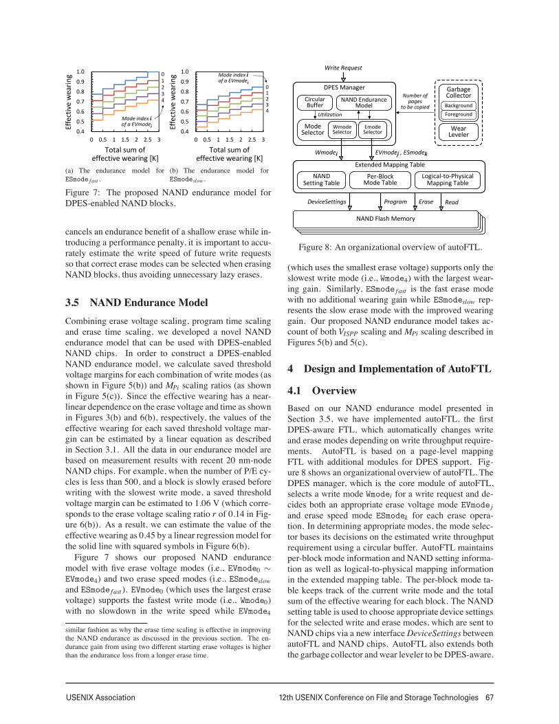
Figure 7: The proposed NAND endurance model forDPES-enabled NAND blocks.
cancels an endurance benefit of a shallow erase while in-troducing a performance penalty, it is important to accu-rately estimate the write speed of future write requestsso that correct erase modes can be selected when erasingNAND blocks, thus avoiding unnecessary lazy erases.
3.5 NAND Endurance ModelCombining erase voltage scaling, program time scalingand erase time scaling, we developed a novel NANDendurance model that can be used with DPES-enabledNAND chips. In order to construct a DPES-enabledNAND endurance model, we calculate saved thresholdvoltage margins for each combination of write modes (asshown in Figure 5(b)) and MPi scaling ratios (as shownin Figure 5(c)). Since the effective wearing has a near-linear dependence on the erase voltage and time as shownin Figures 3(b) and 6(b), respectively, the values of theeffective wearing for each saved threshold voltage mar-gin can be estimated by a linear equation as describedin Section 3.1. All the data in our endurance model arebased on measurement results with recent 20 nm-nodeNAND chips. For example, when the number of P/E cy-cles is less than 500, and a block is slowly erased beforewriting with the slowest write mode, a saved thresholdvoltage margin can be estimated to 1.06 V (which corre-sponds to the erase voltage scaling ratio r of 0.14 in Fig-ure 6(b)). As a result, we can estimate the value of theeffective wearing as 0.45 by a linear regression model forthe solid line with squared symbols in Figure 6(b).
Figure 7 shows our proposed NAND endurancemodel with five erase voltage modes (i.e., EVmode0 ∼EVmode4) and two erase speed modes (i.e., ESmodeslowand ESmode f ast ). EVmode0 (which uses the largest erasevoltage) supports the fastest write mode (i.e., Wmode0)with no slowdown in the write speed while EVmode4
similar fashion as why the erase time scaling is effective in improvingthe NAND endurance as discussed in the previous section. The en-durance gain from using two different starting erase voltages is higherthan the endurance loss from a longer erase time.
Utilization
Write Request
Logical-to-PhysicalMapping Table
NAND Flash Memory
WearLeveler
DPES Manager GarbageCollectorBackgroundForeground
Number of pages
to be copied
Per-BlockMode Table
NANDSetting Table
EVmodej , ESmodek
Extended Mapping Table
DeviceSettings
ModeSelector
NAND Endurance Model
Circular Buffer
Program Erase
Wmode Selector
Emode Selector
Wmodei
Read
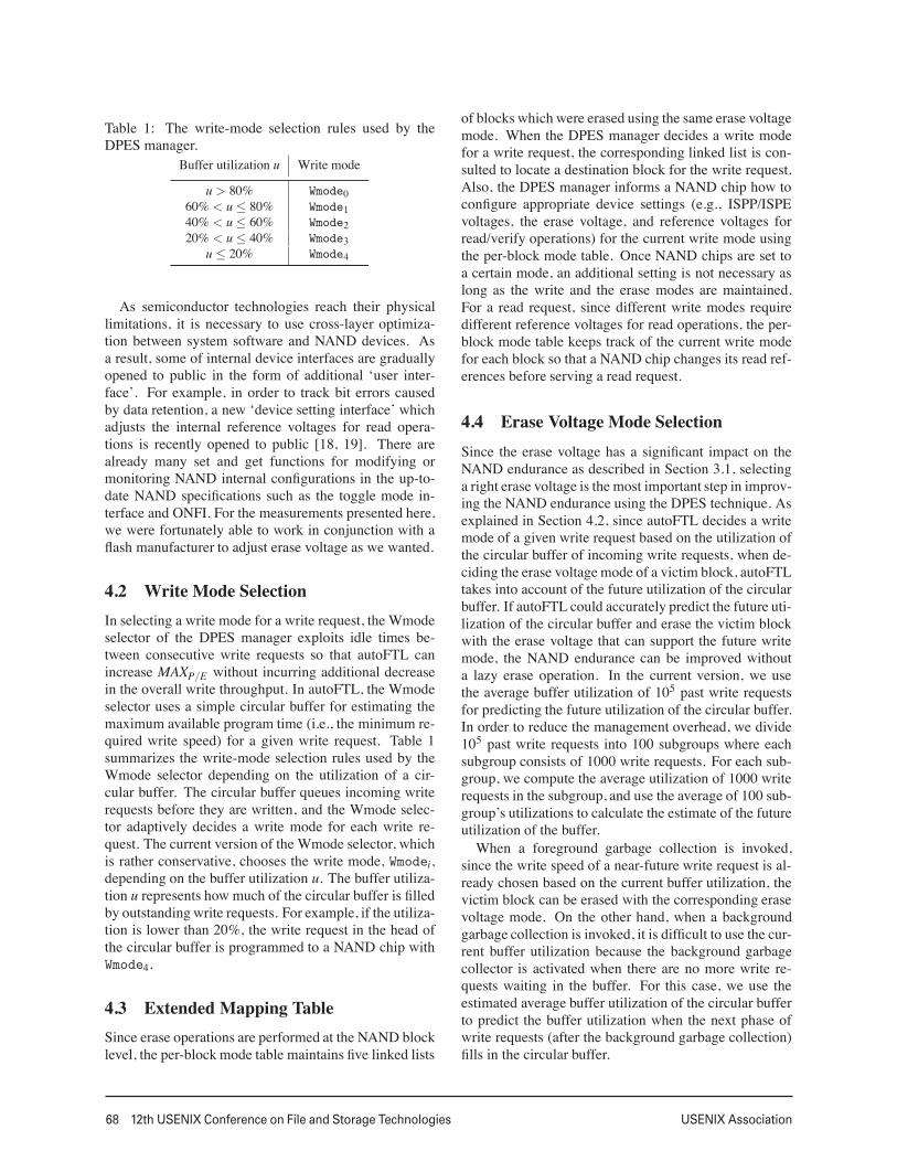
Figure 8: An organizational overview of autoFTL.
(which uses the smallest erase voltage) supports only theslowest write mode (i.e., Wmode4) with the largest wear-ing gain. Similarly, ESmode f ast is the fast erase modewith no additional wearing gain while ESmodeslow rep-resents the slow erase mode with the improved wearinggain. Our proposed NAND endurance model takes ac-count of both VISPP scaling and MPi scaling described inFigures 5(b) and 5(c).
4 Design and Implementation of AutoFTL
4.1 OverviewBased on our NAND endurance model presented inSection 3.5, we have implemented autoFTL, the firstDPES-aware FTL, which automatically changes writeand erase modes depending on write throughput require-ments. AutoFTL is based on a page-level mappingFTL with additional modules for DPES support. Fig-ure 8 shows an organizational overview of autoFTL. TheDPES manager, which is the core module of autoFTL,selects a write mode Wmodei for a write request and de-cides both an appropriate erase voltage mode EVmode jand erase speed mode ESmodek for each erase opera-tion. In determining appropriate modes, the mode selec-tor bases its decisions on the estimated write throughputrequirement using a circular buffer. AutoFTL maintainsper-block mode information and NAND setting informa-tion as well as logical-to-physical mapping informationin the extended mapping table. The per-block mode ta-ble keeps track of the current write mode and the totalsum of the effective wearing for each block. The NANDsetting table is used to choose appropriate device settingsfor the selected write and erase modes, which are sent toNAND chips via a new interface DeviceSettings betweenautoFTL and NAND chips. AutoFTL also extends boththe garbage collector and wear leveler to be DPES-aware.
7
68 12th USENIX Conference on File and Storage Technologies USENIX Association
Table 1: The write-mode selection rules used by theDPES manager.
Buffer utilization u Write mode
u > 80% Wmode060% < u ≤ 80% Wmode140% < u ≤ 60% Wmode220% < u ≤ 40% Wmode3
u ≤ 20% Wmode4
As semiconductor technologies reach their physicallimitations, it is necessary to use cross-layer optimiza-tion between system software and NAND devices. Asa result, some of internal device interfaces are graduallyopened to public in the form of additional ‘user inter-face’. For example, in order to track bit errors causedby data retention, a new ‘device setting interface’ whichadjusts the internal reference voltages for read opera-tions is recently opened to public [18, 19]. There arealready many set and get functions for modifying ormonitoring NAND internal configurations in the up-to-date NAND specifications such as the toggle mode in-terface and ONFI. For the measurements presented here,we were fortunately able to work in conjunction with aflash manufacturer to adjust erase voltage as we wanted.
4.2 Write Mode SelectionIn selecting a write mode for a write request, the Wmodeselector of the DPES manager exploits idle times be-tween consecutive write requests so that autoFTL canincrease MAXP/E without incurring additional decreasein the overall write throughput. In autoFTL, the Wmodeselector uses a simple circular buffer for estimating themaximum available program time (i.e., the minimum re-quired write speed) for a given write request. Table 1summarizes the write-mode selection rules used by theWmode selector depending on the utilization of a cir-cular buffer. The circular buffer queues incoming writerequests before they are written, and the Wmode selec-tor adaptively decides a write mode for each write re-quest. The current version of the Wmode selector, whichis rather conservative, chooses the write mode, Wmodei,depending on the buffer utilization u. The buffer utiliza-tion u represents how much of the circular buffer is filledby outstanding write requests. For example, if the utiliza-tion is lower than 20%, the write request in the head ofthe circular buffer is programmed to a NAND chip withWmode4.
4.3 Extended Mapping TableSince erase operations are performed at the NAND blocklevel, the per-block mode table maintains five linked lists
of blocks which were erased using the same erase voltagemode. When the DPES manager decides a write modefor a write request, the corresponding linked list is con-sulted to locate a destination block for the write request.Also, the DPES manager informs a NAND chip how toconfigure appropriate device settings (e.g., ISPP/ISPEvoltages, the erase voltage, and reference voltages forread/verify operations) for the current write mode usingthe per-block mode table. Once NAND chips are set toa certain mode, an additional setting is not necessary aslong as the write and the erase modes are maintained.For a read request, since different write modes requiredifferent reference voltages for read operations, the per-block mode table keeps track of the current write modefor each block so that a NAND chip changes its read ref-erences before serving a read request.
4.4 Erase Voltage Mode SelectionSince the erase voltage has a significant impact on theNAND endurance as described in Section 3.1, selectinga right erase voltage is the most important step in improv-ing the NAND endurance using the DPES technique. Asexplained in Section 4.2, since autoFTL decides a writemode of a given write request based on the utilization ofthe circular buffer of incoming write requests, when de-ciding the erase voltage mode of a victim block, autoFTLtakes into account of the future utilization of the circularbuffer. If autoFTL could accurately predict the future uti-lization of the circular buffer and erase the victim blockwith the erase voltage that can support the future writemode, the NAND endurance can be improved withouta lazy erase operation. In the current version, we usethe average buffer utilization of 105 past write requestsfor predicting the future utilization of the circular buffer.In order to reduce the management overhead, we divide105 past write requests into 100 subgroups where eachsubgroup consists of 1000 write requests. For each sub-group, we compute the average utilization of 1000 writerequests in the subgroup, and use the average of 100 sub-group’s utilizations to calculate the estimate of the futureutilization of the buffer.
When a foreground garbage collection is invoked,since the write speed of a near-future write request is al-ready chosen based on the current buffer utilization, thevictim block can be erased with the corresponding erasevoltage mode. On the other hand, when a backgroundgarbage collection is invoked, it is difficult to use the cur-rent buffer utilization because the background garbagecollector is activated when there are no more write re-quests waiting in the buffer. For this case, we use theestimated average buffer utilization of the circular bufferto predict the buffer utilization when the next phase ofwrite requests (after the background garbage collection)fills in the circular buffer.
8

USENIX Association 12th USENIX Conference on File and Storage Technologies 69
4.5 Erase Speed Mode SelectionIn selecting an erase speed mode for a block erase oper-ation, the DPES manager selects an erase speed modewhich does not affect the write throughput. An erasespeed mode for erasing a NAND block is determined byestimating the effect of a block erase time on the bufferutilization. Since write requests in the circular buffercannot be programmed while erasing a NAND block,the buffer utilization is effectively increased by the blockerase time. The effective buffer utilization u′ consider-ing the effect of the block erase time can be expressed asfollows:
u′ = u+∆uerase, (3)
where u is the current buffer utilization and ∆uerase isthe increment in the buffer utilization by the block erasetime. In order to estimate the effect of a block erase op-eration on the buffer utilization, we convert the blockerase time to a multiple M of the program time of thecurrent write mode. ∆uerase corresponds to the incrementin the buffer utilization for these M pages. For select-ing an erase speed mode of a NAND block, the modeselector checks if ESmodeslow can be used. If erasingwith ESmodeslow does not increase u′ larger than 100%(i.e., no buffer overflow), ESmodeslow is selected. Other-wise, the fast erase mode ESmode f ast is selected. On theother hand, when the background garbage collection isinvoked, ESmodeslow is always selected in erasing a vic-tim block. Since the background garbage collection isinvoked when an idle time between consecutive write re-quests is sufficiently long, the overall write throughput isnot affected even with ESmodeslow.
4.6 DPES-Aware Garbage CollectionWhen the garbage collector is invoked, the most appro-priate write mode for copying valid data to a free block isdetermined by using the same write-mode selection rulessummarized in Table 1 with a slight modification to com-puting the buffer utilization u. Since the write requests inthe circular buffer cannot be programmed while copyingvalid pages to a free block by the garbage collector, thebuffer utilization is effectively increased by the numberof valid pages in a victim block. By using the informa-tion from the garbage collector, the mode selector recal-culates the effective buffer utilization u∗ as follows:
u∗ = u+∆ucopy, (4)
where u is the current buffer utilization and ∆ucopy is theincrement in the buffer utilization taking the number ofvalid pages to be copied into account. The mode selectordecides the most appropriate write mode based on thewrite-mode selection rules with u∗ instead of u. Aftercopying all the valid pages to a free block, a victim blockis erased by the erase voltage mode (selected by the rules
Table 2: Examples of selecting write and erase modesin the garbage collector assuming that the circular bufferhas 200 pages and the current buffer utilization u is 70%.
(Case 1) The number of valid pages in a victim block is 30.
ucopy u∗ ∆uerase u′ Selectedmodes
15% 85%Slow 8% 93% EVmode0 & ESmodeslow
Fast 2% 87% Wmode0
(Case 2) The number of valid pages in a victim block is 50.
ucopy u∗ ∆uerase u′ Selectedmodes
25% 95%Slow 8% 103% EVmode0 & ESmode f ast
Fast 2% 97% Wmode0
described in Section 4.4) with the erase speed (chosenby the rules described in Section 4.5). For example, asshown in the case 1 of Table 2, if garbage collection isinvoked when u is 70%, and the number of valid pages tobe copied is 30 (i.e., ∆ucopy
= 30/200 = 15%), Wmode0is selected because u∗ is 85% (= 70% + 15%), andESmodeslow is selected because erasing with ESmodeslowdoes not overflow the circular buffer. (We assume that∆uerase for ESmodeslow and ∆uerase for ESmode f ast are 8%and 2%, respectively.) On the other hand, as shown in thecase 2 of Table 2, when the number of valid pages to becopied is 50 (i.e., ∆ucopy
= 50/200 = 25%), ESmodeslowcannot be selected because u′ becomes larger than 100%.As shown in the case 1, ESmodeslow can still be used evenwhen the buffer utilization is higher than 80%. Whenthe buffer utilization is higher than 80% (i.e., an inten-sive write workload condition), the erase voltage scalingis not effective because the highest erase voltage is se-lected. On the other hand, even when the buffer utiliza-tion is above 90%, the erase speed scaling can be stilluseful.
4.7 DPES-Aware Wear Leveling
Since different erase voltage/time affects the NAND en-durance differently as described in Section 3.1, the relia-bility metric (based on the number of P/E cycles) of theexisting wear leveling algorithm [20] is no longer validin a DPES-enabled NAND flash chip. In autoFTL, theDPES-aware wear leveler uses the total sum of the ef-fective wearing instead of the number of P/E cycles as areliability metric, and tries to evenly distribute the totalsum of the effective wearing among NAND blocks.
9

70 12th USENIX Conference on File and Storage Technologies USENIX Association
5 Experimental Results
5.1 Experimental Settings
In order to evaluate the effectiveness of the proposed aut-oFTL, we used an extended version of a unified develop-ment environment, called FlashBench [12], for NANDflash-based storage devices. Since the efficiency of ourDPES is tightly related to the temporal characteristicsof write requests, we extended the existing FlashBenchto be timing-accurate. Our extended FlashBench em-ulates the key operations of NAND flash memory in atiming-accurate fashion using high-resolution timers (orhrtimers) (which are available in a recent Linux kernel[21]). Our validation results on an 8-core Linux serversystem show that the extended FlashBench is very accu-rate. For example, variations on the program time anderase time of our DRAM-based NAND emulation mod-els are less than 0.8% of TPROG and 0.3% of TERASE , re-spectively.
For our evaluation, we modified a NAND flash modelin FlashBench to support DPES-enabled NAND flashchips with five write modes, five erase voltage modes,and two erase speed modes as shown in Figure 7. EachNAND flash chip employed 128 blocks which were com-posed of 128 8-KB pages. The maximum number ofP/E cycles was set to 3,000. The nominal page programtime (i.e., TPROG) and the nominal block erase time (i.e.,TERASE) were set to 1.3 ms and 5.0 ms, respectively.
We evaluated the proposed autoFTL in two differ-ent environments, mobile and enterprise environments.Since the organizations of mobile storage systems andenterprise storage systems are quite different, we usedtwo FlashBench configurations for different environ-ments as summarized in Table 3. For a mobile envi-ronment, FlashBench was configured to have two chan-nels, and each channel has a single NAND chip. Sincemobile systems are generally resource-limited, the sizeof a circular buffer for a mobile environment was setto 80 KB only (i.e., equivalently 10 8-KB pages). Foran enterprise environment, FlashBench was configuredto have eight channels, each of which was composed offour NAND chips. Since enterprise systems can utilizemore resources, the size of a circular buffer was set to 32MB (which is a typical size of data buffer in HDD) forenterprise environments.
We carried out our evaluations with two different tech-niques: baseline and autoFTL. Baseline is an existingDPES-unaware FTL that always uses the highest erasevoltage mode and the fast erase mode for erasing NANDblocks, and the fastest write mode for writing data toNAND blocks. AutoFTL is the proposed DPES-awareFTL which decides the erase voltage and the erase timedepending on the characteristic of a workload and fullyutilizes DPES-aware techniques, described in Sections 3
Table 3: Summary of two FlashBench configurations.Environments Channels Chips Buffer
Mobile 2 2 80 KB
Enterprise 8 32 32 MB
and 4, so it can maximally exploit the benefits of dy-namic program and erase scaling.
Our evaluations were conducted with various I/Otraces from mobile and enterprise environments. (Formore details, please see Section 5.2). In order to re-play I/O traces on top of the extended FlashBench, wedeveloped a trace replayer. The trace replayer fetchesI/O commands from I/O traces and then issues them tothe extended FlashBench according to their inter-arrivaltimes to a storage device. After running traces, we mea-sured the maximum number of P/E cycles, MAXP/E ,which was actually conducted until flash memory be-came unreliable. We then compared it with that of base-line. The overall write throughput is an important metricthat shows the side-effect of autoFTL on storage perfor-mance. For this reason, we also measured the overallwrite throughput while running each I/O trace.
5.2 BenchmarksWe used 8 different I/O traces collected from Android-based smartphones and real-world enterprise servers.The m down trace was recorded while downloading asystem installation file (whose size is about 700 MB)using a mobile web-browser through 3G network. Them p2p1 trace included I/O activities when downloadingmultimedia files using a mobile P2P application from alot of rich seeders. Six enterprise traces, hm 0, proj 0,prxy 0, src1 2, stg 0, and web 0, were from the MS-Cambridge benchmarks [22]. However, since enterprisetraces were collected from old HDD-based server sys-tems, their write throughputs were too low to evaluatethe performance of modern NAND flash-based storagesystems. In order to partially compensate for low writethroughput of old HDD-based storage traces, we accel-erated all the enterprise traces by 100 times so that thepeak throughput of the most intensive trace (i.e., src1 2)can fully consume the maximum write throughput of ourNAND configuration. (In our evaluations, therefore, allthe enterprise traces are 100x-accelerated versions of theoriginal traces.)
Since recent enterprise SSDs utilize lots of inter-chip parallelism (multiple channels) and intra-chip paral-lelism (multiple planes), peak throughput is significantlyhigher than that of conventional HDDs. We tried to findappropriate enterprise traces which satisfied our require-ments to (1) have public confidence; (2) can fully con-sume the maximum throughput of our NAND configura-
10

USENIX Association 12th USENIX Conference on File and Storage Technologies 71
Table 4: Normalized inter-arrival times of write requestsfor 8 traces used for evaluations.
TraceDistributions of normalized
inter-arrival times t over T e f f ectivePROG [%]
t ≤ 1 1 <t≤ 2 t > 2
proj 0 40.6% 47.0% 12.4%src1 2 41.0% 55.6% 3.4%hm 0 14.2% 72.1% 13.7%prxy 0 8.9% 34.6% 56.5%stg 0 7.1% 81.5% 11.4%web 0 5.4% 36.7% 56.9%m down 45.9% 0.0% 54.1%m p2p1 49.5% 0.0% 50.5%
tion; (3) reflect real user behaviors in enterprise environ-ments; (4) are extracted from under SSD-based storagesystems. To the best of our knowledge, we could not findany workload which met all of the requirements at thesame time. In particular, there are few enterprise SSDworkloads which are opened to public.
Table 4 summarizes the distributions of inter-arrivaltimes of our I/O traces. Inter-arrival times were normal-ized over T e f f ective
PROG which reflects parallel NAND opera-tions supported by multiple channels and multiple chipsper channel in the extended FlashBench. For example,for an enterprise environment, since up to 32 chips canserve write requests simultaneously, T e f f ective
PROG is about40 us (i.e., 1300 us of TPROG is divided by 32 chips.).On the other hand, for a mobile environment, since thereare only 2 chips can serve write requests at the sametime, T e f f ective
PROG is 650 us. Although the mobile tracescollected from Android smartphones (i.e., m down [23]and m p2p1) exhibit very long inter-arrival times, nor-malized inter-arrival times over T e f f ective
PROG are not muchdifferent from the enterprise traces, except that the mo-bile traces show distinct bimodal distributions which nowrite requests in 1 <t≤ 2.
5.3 Endurance Gain Analysis
In order to understand how much MAXP/E is improvedby DPES, each trace was repeated until the total sumof the effective wearing reached 3K. Measured MAXP/Evalues were normalized over that of baseline. Figure 9shows normalized MAXP/E ratios for eight traces withtwo different techniques. Overall, the improvement onMAXP/E is proportional to inter-arrival times as summa-rized in Table 4; the longer inter-arrival times are, themore likely slow write modes are selected.
AutoFTL improves MAXP/E by 69%, on average, overbaseline for the enterprise traces. For proj 0 and src1 2
traces, improvements on MAXP/E are less than 50% be-cause inter-arrival times of more than 40% of write re-quests are shorter than T e f f ective
PROG so that it is difficult to
0.0
0.5
1.0
1.5
2.0
2.5
3.0Baseline AutoFTL
Nor
mal
ized MAX
P/E
ratio
+46%
Avg. +69%
+50%+76% +82% +78% +80%
+39% +37%
Avg. +38%
Figure 9: Comparisons of normalized MAXP/E ratios foreight traces.
0.0
0.5
1.0
1.5Baseline AutoFTL
Nor
mal
ized
over
all
writ
e th
roug
hput -2.17%
Avg. -0.91%
-0.66% -0.64% -1.49% -0.14% -0.36% -0.09% -0.03%Avg. -0.06%
Figure 10: Comparisons of normalized overall writethroughputs for eight traces.
use the lowest erase voltage mode. For the other enter-prise traces, MAXP/E is improved by 79%, on average,over baseline.
On the other hand, for the mobile traces, AutoFTL im-proves MAXP/E by only 38%, on average, over baseline.Although more than 50% of write requests have inter-arrival times twice longer than T e f f ective
PROG , autoFTL couldnot improve MAXP/E as much as expected. This is be-cause the size of the circular buffer is too small for buffer-ing the increase in the buffer utilization caused by thegarbage collection. For example, when a NAND block iserased by the fast speed erase mode, the buffer utilizationis increased by 40% for the mobile environment whilethe effect of the fast erase mode on the buffer utilizationis less than 0.1% for the enterprise environment. More-over, by the same reason, the slow erase speed mode can-not be used in the mobile environment.
5.4 Overall Write Throughput AnalysisAlthough autoFTL uses slow write modes frequently, thedecrease in the overall write throughput over baseline isless than 2.2% as shown in Figure 10. For proj 0 trace,the overall write throughput is decreased by 2.2%. Thisis because, in proj 0 trace, the circular buffer may be-come full by highly clustered write requests. When thecircular buffer becomes full, if the foreground garbagecollection should be invoked, the write response time ofNAND chips can be directly affected. Although inter-arrival times in prxy 0 trace are relatively long overother enterprise traces, the overall write throughput is
11

72 12th USENIX Conference on File and Storage Technologies USENIX Association
0.0
0.2
0.4
0.6
0.8
1.0EVmode0 EVmode1 EVmode2 EVmode3 EVmode4
Dist
ribut
ions
of E
Vmod
e's
Figure 11: Distributions of EVmode’s used.
degraded more than the other enterprise traces. This isbecause almost all the write requests exhibit inter-arrivaltimes shorter than 10 ms so that the background garbagecollection is not invoked at all4. As a result, the fore-ground garbage collection is more frequently invoked,thus increasing the write response time.
We also evaluated if there is an extra delay from ahost in sending a write request to the circular buffer be-cause of DPES. Although autoFTL introduced a few ex-tra queueing delay for the host, the increase in the aver-age queueing delay per request was negligible comparedto T e f f ective
PROG . For example, for src1 2 trace, 0.4% of thetotal programmed pages were delayed, and the averagequeueing delay per request was 2.6 us. For stg 0 trace,less than 0.1% of the total programmed pages were de-layed, and the average queueing delay per request was0.1 us.
5.5 Detailed AnalysisWe performed a detailed analysis on the relationship be-tween the erase voltage/speed modes and the improve-ment of MAXP/E . Figure 11 presents distributions ofEVmode’s used for eight I/O traces. Distributions ofEVmode’s exactly correspond to the improvements ofMAXP/E as shown in Figure 9; the more frequently a lowerase voltage mode is used, the higher the endurance gainis. In our evaluations for eight I/O traces, lazy erases arerarely used for all the traces.
Figure 12(a) shows distributions of ESmode’s for eightI/O traces. Since the slow erase mode is selected by us-ing the effective buffer utilization, there are little chancesfor selecting the slow erase mode for the mobile tracesbecause the size of the circular buffer is only 80 KB.On the other hand, for the enterprise environment, thereare more opportunities for selecting the slow erase mode.Even for the traces with short inter-arrival times such asproj 0 and src1 2, only 5%∼10% of block erases usedthe fast erase mode.
We also evaluated the effect of the slow erase modeon the improvement of MAXP/E . For this for evaluation,
4In our autoFTL setting, the background garbage collection is in-voked when a idle time between two consecutive requests is longer than300 ms.
0.0
0.2
0.4
0.6
0.8
1.0ESmode ESmode
Dist
ribut
ions
of E
Smod
e's fast slow
(a) Distributions of ESmode’s used.
0.0
0.5
1.0
1.5
2.0
2.5
3.0
proj_0 src1_2 hm_0 prxy_0 stg_0 web_0
AutoFTL AutoFTL
Nor
mal
ized MAX
P/E
ratio
+14% +13%+17% +17% +18% +17%
_
(b) The effect of ESmodeslow on improving MAXP/E .
Figure 12: Distributions of ESmode’s used and the effectof ESmode’s on MAXP/E .
we modified our autoFTL so that ESmode f ast is alwaysused when NAND blocks are erased. (We represent thistechnique by autoFTL
−.) As shown in Figure 12(b), theslow erase mode can improve the NAND endurance gainup to 18%. Although the slow erase mode can increasethe buffer utilization, its effect on the write throughputwas almost negligible.
6 Related Work
As the endurance of recent high-density NAND flashmemory is continuously reduced, several system-leveltechniques which exploit the physical characteristics ofNAND flash memory have been proposed for improv-ing the endurance and lifetime of flash-based storage sys-tems [8, 7, 24, 25].
Mohan et al. investigated the effect of the damagerecovery on the SSD lifetime for enterprise servers [8].They showed that the overall endurance of NAND flashmemory can be improved with its recovery nature. OurDPES technique does not consider the self-recovery ef-fect, but it can be easily extended to exploit the physicalcharacteristic of the self-recovery of flash memory cells.
Lee et al. proposed a novel lifetime management tech-nique that guarantees the lifetime of storage devices byintentionally throttling write performance [7]. They alsoexploited the self-recovery effect of NAND devices, soas to lessen the performance penalty caused by writethrottling. Unlike Lee’s work (which sacrifices writeperformance for guaranteeing the storage lifetime), ourDPES technique improves the lifetime of NAND deviceswithout degrading the performance of NAND-based stor-
12

USENIX Association 12th USENIX Conference on File and Storage Technologies 73
age systems.
Wu et al. presented a novel endurance enhancementtechnique that boosts recovery speed by heating a flashchip under high temperature [24]. By leveraging thetemperature-accelerated recovery, it improved the en-durance of SSDs up to five times. The major drawback ofthis approach is that it requires extra energy consumptionto heat flash chips and lowers the reliability of a storagedevice. Our DPES technique improves the endurance ofNAND devices by lowering the erase voltage and slow-ing down the erase speed without any serious side effect.
Jeong et al. proposed an earlier version of theDPES idea and demonstrated that DPES can improve theNAND endurance significantly without sacrificing theoverall write throughput [25]. Unlike their work, how-ever, our work treats the DPES approach in a more com-plete fashion, extensively extending the DPES approachin several dimensions such as the erase speed scaling,shallow erasing and lazy erase scheme. Furthermore,more realistic and detailed evaluations using the timing-accurate emulator are presented in this paper.
7 Conclusions
We have presented a new system-level approach for im-proving the lifetime of flash-based storage systems usingdynamic program and erase scaling (DPES). Our DPESapproach actively exploits the tradeoff relationship be-tween the NAND endurance and the erase voltage/speedso that directly improves the NAND endurance with aminimal decrease in the write performance. Based onour novel NAND endurance model and the newly definedinterface for changing the NAND behavior, we have im-plemented autoFTL, which changes the erase voltage andspeed in an automatic fashion. Moreover, by makingthe key FTL modules (such as garbage collection andwear leveling) DPES-aware, autoFTL can significantlyimprove the NAND endurance. Our experimental resultsshow that autoFTL can improve the maximum number ofP/E cycles by 69% for enterprise traces and 38% for mo-bile traces, on average, over an existing DPES-unawareFTL.
The current version of autoFTL can be further im-proved in several ways. For example, we believe that thecurrent mode selection rules are rather too conservativewithout adequately reflecting the varying characteristicsof I/O workload. As an immediate future task, we planto develop more adaptive mode selection rules that mayadaptively adjust the buffer utilization boundaries for se-lecting write modes.
Acknowledgements
We would like to thank Erik Riedel, our shepherd, andanonymous referees for valuable comments that greatlyimproved our paper. This work was supported by theNational Research Foundation of Korea (NRF) grantfunded by the Ministry of Science, ICT and Future Plan-ning (MSIP) (NRF-2013R1A2A2A01068260). This re-search was also supported by Next-Generation Infor-mation Computing Development Program through NRFfunded by MSIP (No. 2010-0020724). The ICT at SeoulNational University and IDEC provided research facili-ties for this study.
References
[1] S.-H. Shin et al., “A New 3-bit Programming Al-gorithm Using SLC-to-TLC Migration for 8 MB/sHigh Performance TLC NAND Flash Memory,” inProc. IEEE Symp. VLSI Circuits, 2012.
[2] J. Choi et al., “3D Approaches for Non-volatileMemory,” in Proc. IEEE Symp. VLSI Technology,2011.
[3] A. A. Chien et al., “Moore’s Law: The First End-ing and A New Beginning,” Tech. Report, Dept. ofComputer Science, the Univ. of Chicago, TR-2012-06.
[4] J.-W. Hsieh et al., “Efficient Identification of HotData for Flash Memory Storage Systems,” ACMTrans. Storage, vol. 2, no. 1, pp. 22-40, 2006.
[5] F. Chen et al., “CAFTL: A Content-Aware FlashTranslation Layer Enhancing the Lifespan of FlashMemory Based Solid State Drives,” in Proc.USENIX Conf. File and Storage Tech., 2011.
[6] S. Lee et al., “Improving Performance and Lifetimeof Solid-State Drives Using Hardware-AcceleratedCompression,” IEEE Trans. Consum. Electron.,vol. 57, no. 4, pp. 1732-1739, 2011.
[7] S. Lee et al., “Lifetime Management of Flash-Based SSDs Using Recovery-Aware DynamicThrottling,” in Proc. USENIX Conf. File and Stor-age Tech., 2012.
[8] V. Mohan et al., “How I Learned to Stop Worry-ing and Love Flash Endurance,” in Proc. USENIXWorkshop Hot Topics in Storage and File Systems,2010.
[9] N. Mielke et al., “Bit Error Rate in NAND FlashMemories,” in Proc. IEEE Int. Reliability PhysicsSymp., 2008.
13

74 12th USENIX Conference on File and Storage Technologies USENIX Association
[10] K. F. Schuegraf et al., “Effects of Temperature andDefects on Breakdown Lifetime of Thin SiO2 atVery Low Voltages,” IEEE Trans. Electron Devices,vol. 41, no. 7, pp. 1227-1232, 1994.
[11] S. Cho, “Improving NAND Flash Memory Relia-bility with SSD Controllers,” in Proc. Flash Mem-ory Summit, 2013.
[12] S. Lee et al., “FlashBench: A Workbench for aRapid Development of Flash-Based Storage De-vices,” in Proc. IEEE Int. Symp. Rapid System Pro-totyping, 2012.
[13] R.-S. Liu et al., “Optimizing NAND Flash-BasedSSDs via Retention Relaxation,” in Proc. USENIXConf. File and Storage Tech., 2012.
[14] K.-D. Suh et al., “A 3.3 V 32 Mb NAND FlashMemory with Incremental Step Pulse ProgrammingScheme,” IEEE J. Solid-State Circuits, vol. 30, no.11, pp. 1149-1156, 1995.
[15] JEDEC Standard, ”Stress-Test-Driven Qualifica-tion of Integrated Circuits,” JESD47H.01, 2011.
[16] J. Jeong and J. Kim, “Dynamic Program andErase Scaling in NAND Flash-based StorageSystems,” Tech. Report, Seoul National Univ.,http://cares.snu.ac.kr/download/TR-CARES-01-14, 2014.
[17] D.-W. Lee et al., “The Operation Algorithm for Im-proving the Reliability of TLC (Triple Level Cell)NAND Flash Characteristics,” in Proc. IEEE Int.Memory Workshop, 2011.
[18] J. Yang, “High-Efficiency SSD for Reliable DataStorage Systems,” in Proc. Flash Memory Summit,2011.
[19] R. Frickey, “Data Integrity on 20 nm NAND SSDs,”in Proc. Flash Memory Summit, 2012.
[20] L.-P. Chang, “On Efficient Wear Leveling forLarge-Scale Flash-Memory Storage Systems,” inProc. ACM Symp. Applied Computing, 2007.
[21] IBM “Kernel APIs, Part 3: Timers and Lists in the2.6 Kernel,” http://www.ibm.com/developerworks/library/l-timers-list/.
[22] D. Narayanan et al., “Write Off-Loading: Practi-cal Power Management for Enterprise Storage,” inProc. USENIX Conf. File and Storage Tech., 2008.
[23] http://www.ubuntu.com/download
[24] Q. Wu et al., “Exploiting Heat-Accelerated FlashMemory Wear-Out Recovery to Enable Self-Healing SSDs,” in Proc. USENIX Workshop HotTopics in Storage and File Systems, 2011.
[25] J. Jeong et al., “Improving NAND Endurance byDynamic Program and Erase scaling,” in Proc.USENIX Workshop Hot Topics in Storage and FileSystems, 2013.
14