lf2 jj3 a novel transition between rectangular waveguide
TRANSCRIPT

NASA Technical Memorandum 106661 /57:2
,p
Lf2 JJ3 A Novel Transition Between Rectangular Waveguide and Layered Ridge Dielectric Waveguide
George E. Ponchak Lewis Research Center Cleveland, Ohio
and
Nihad 1. Dib and Linda P.B. Katehi University of Michigan Ann Arbor, Michigan
Prepared for the European Microwave Conference cosponsored by the Institute of Electrical Engineers and Institute of Electrical and Electronics Engineers Cannes, France, September 5-8, 1994
e,""'" .. ., ... .. , '" ~ - ' ~ '
" National Aeronautics and Space Administration
( NASA -TM-I066 61) A NOVEL TRANSITION BETWEEN RECTANGULAR WAVEGUIDE A 0 LAYERED RIDGE O IELECT~IC WAVEGUIDE (NASA. Lewis Research Center) 7 p
N94-36955
Unclas
G3/32 0015728

r !
A NOVEL TRANSmON BETWEEN RECTANGULAR WAVEGUIDE AND LAYERED RIDGE DIELECTRIC WAVEGUIDE
George E. Ponchak National Aeronautics and Space Administration
Lewis Research Center Cleveland, Ohio 44135
ABSTRACT
Nihad 1. Dib and Linda P. B. Katehi Radiation Laboratory
Department of Electrical Engineering and Computer Science University of Michigan
Ann Arbor, Michigan 48109-2122
A novel transition between rectangular waveguide and Layered Ridge Dielectric Waveguide (LRDW) is reported. The transition is also suitable for use with Image Guide, Insulated Image Guide, Dielectric Ridge Waveguide and other open dielectric waveguides. Both experimental and theoretical data are presented which compare the new transition to three transitions reported in the literature.
INTRODIICTION An efficient transition between dielectric waveguide and rectangular waveguide is critical for interconnecting dielectric waveguides such as image guide [1], insulated image guide [2], trapped image guide [3], ridge guide [4], and layered ridge dielectric waveguide (LRDW)[5,6] to test equipment and millimeter-wave sources such as Gunn diodes which typically have a rectangular waveguide output port. For open dielectric waveguides, the transition must not only match the impedances of the two different transmission lines but must also transform the fields from the well confined rectangular waveguide to the weakly confined open dielectric waveguides . In addition, the radiation loss from the open waveguide must be minimized to obtain a low insertion loss. Transition designs are especially difficult when high permittivity materials or layered ridges are used to fabricate electrically small dielectric waveguides. An example is the LRDW designed for Ka-Band shown in Figure 1. This dielectric waveguide is A.o/lO high and "A.o/5 wide at 30 GHz. All results presented in this paper are developed for transitions to the LRDW shown in Figure 1.
Three types of transitions from rectangular waveguide to open dielectric waveguides have been reported in the literature. These may all be considered as variations of the transition shown in Figure 2a. In the first transition, referred to as A in the rest of the paper, the full height rectangular waveguide is butted directly to the dielectric waveguide. The second transition, referred to as B in the rest of the paper, incorporates a taper to reduced height waveguide. The dielectric waveguide is then butted directly to the reduced height rectangular waveguide. Since the height of the rectangular waveguide is now closer to the height of the dielectric waveguide, the field interaction is stronger and lower insertion loss is expected. Finally, a hom is added to impedance match the shielded dielectric waveguide to the open dielectric waveguide. This transition will be referred to as C throughout the rest of the paper. In each of the transition designs, a dielectric wedge or tapered section of the dielectric waveguide may be used to reduce the reflection from the transition [1].
This paper presents a new transition, shown in Figure 2b, from rectangular waveguide to open dielectric waveguide. A tapered ridge waveguide section is used to confine the power in the rectangular waveguide to an area equal to the width of the dielectric waveguide. The ridge is then continued into the horn section of the transition for impedance matching to the open dielectric waveguide. Since the ridge waveguide section localizes the fields better than the reduced height waveguide, the ridge waveguide transition has lower insertion loss and reduced radiation. This transition will be referred to as transition D in the rest of the paper.
ExPERIMENTAl , CHARACTERIZATION Experimental characterization of the transitions was performed on an HP 8510B Vector Network Analyzer with a WR-28 Reflection/Transmission test set. The measurement system was calibrated to the end of the WR-28 rectangular waveguide using the open, short, load calibration technique. To verify that any reflected power was due to the transition and not flaws in the dielectric waveguide, the time domain feature of the ANA was used to determine where all reflections originated from. The transitions were connected back to back through a 19 cm
--~.---
! J

/
section ofLRDW. The LRDW and the dielectric wedges were fabricated from RT/Duroid 5880, 6006, and 6010 microwave substrates and Rogers 3001 bonding film. Through experimental characterization, the dielectric waveguide has a loss of 0.02 dB/mm.
THEORETICAl. CHAR ACTERlZATION To theoretically characterize the transitions, the Finite Difference Time Domain (FDTD) method was used. Maxwell's curl equations are expressed in discretized space and time domains which are then used to simulate the propagation of an initial excitation in a "leapfrog" manner [7]. The excitation pulse is chosen such that its spectrum has a peak value at 30.5 GHz while the value is reduced to 5% of the peak value at 21 and 40 GHz (the TEID band of the WR-28 rectangular waveguide) [8,9]. The first-order Mur absorbing boundary condition (ABC) is used at the side and top walls surrounding the dielectric waveguide while the super-absorber first-order Mur ABC is implemented at the front and back walls.
RESIILTS The accuracy of the theoretical modeling is demonstrated in Figure 3 which shows the measured and theoretical return loss for transition B with no dielectric wedge. The measured reflected power is lower across the frequency band than theoretically predicted due to the absence of conductor and dielectric loss mechanisms in the theoretical simulations. The maximum difference between the two curves is 2.5 dB . To eliminate the reflected power from the second transition during the experimental measurements, absorbing material was placed over the dielectric waveguide. The time domain feature of the HP8510 was used to verify that no signal was reflected from either the absorbing material or the second transition.
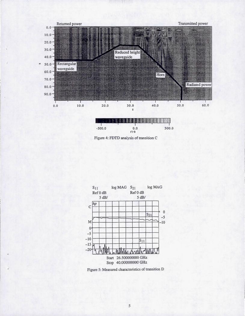
Using the FDTD method, the power reflected from the transition, transmitted through the LRDW, and radiated into free space can be plotted. Figure 4 shows a cross-section of transition C without a dielectric wedge. The power transitioned to the LRDW is clearly shown across the top of the figure. Notice that the power is concentrated in the center layer, the low permittivity layer, of the LRDW. For this transition, the reflected power shown in the rectangular waveguide propagating back towards the source is relatively large. The radiated power, although small, is clearly shown propagating away from the transition faster than the power is propagating in the LRDW.
The best measured performance for each type of transition is shown in Table 1. The Insertion Loss values at 26.5 GHz and 40 GHz are per transition with the loss of the LRDW line subtracted out. The Return Loss value is the maximum value measured across the 26.5-40 GHz band for the back to back connected transitions. The length, height, and relative permittivity of the dielectric wedge are for the optimum characteristics which are given in Table 1. Transition D has the best overall characteristics with a total return loss better than 17.5 dB and an average insertion loss of 1.2 dB across the full waveguide band. The measured RF characteristics of transition D measured in the back to back configuration is shown in Figure 5. Note that the total return loss of transition Dis 5 dB lower than the return loss for transitions A, B, and C. Also, for all four transition types, an optimum dielectric wedge exists which improves the transition characteristics.
CONCI JISIONS Transitions from rectangular waveguide to LRDW have been studied . A new type of transition which uses a ridge waveguide taper in both the rectangular waveguide and the horn section has been shown to have superior performance compared to previously used types of transitions. A maximum insertion loss of 1.5 dB with a 17.5 dB return loss across the 26.5-40 GHz band has been demonstrated.
ACKNOWT EDGEMENTS This work was supported by funds from the ARO (Army Research Office) and the NASA Lewis Research Center Director's Discretionary Fund.
REFERENCES [1] M. Dydyk, "Image guide: a promising medium for EHF circuits," Microwaves, April 1981, pp . 71-80. [2] W. V. McLevige, T. Itoh, and R. Mittra, "New waveguide structures for millimeter-wave circuits,"
IEEE Trans. Microwave Theory Tech., Oct. 1975, pp . 788-794. [3] T. Itoh and B. Adelseck, "Trapped image guide for millimeter-wave circuits," IEEE Trans. Microwave
Theory Tech., Dec. 1980, pp. 1433-1436.
2

I
[4] T. Wang and S. E. Schwarz, "Design of dielectric ridge waveguides for millimeter-wave integrated circuits," IEEE Trans. Microwave Theory Tech., Feb. 1983, pp. 128-134.
[5] A. G. Engel, Jr. and L. P. B. Katehi, "Low-loss monolithic transmission lines for submillimeter and terahertz frequency applications," IEEE Trans. Microwave Theory Tech., Nov. 1991, pp. 1847-1854.
[6] G. E. Ponchak and L. P. B. Katehi, "Development of leaky wave antennas for layered ridge dielectric waveguide," IEEE AP-S Int. Symp Dig .. , Ann Arbor, Michigan, June 28- July 2, 1993, pp. 580-583.
[7] K. Kunz and R. Luebbers, The Finite Difference Time Domain Method for Electromagnetics, Florida: CRC Press, 1993.
[8] N. Dib and L. Katehi, "Analysis of the transition from rectangular waveguide to shielded dielectric image guide using the finite~fference time-domain method," IEEE Microwave and Guided Wave Lett. ," Sept. 1993, pp. 327-329.
[9] N. Dib and L. Katehi, "Characterization of the sub-mm wave dielectric waveguide directional coupler using the FDTD method," 1994 IEEE MTT-S Int. Microwave Symp. Dig., May 1994, pp. 297-300.
Transition ~dge Return Loss (dB) Insertion loss at 26.5 GHz ~nsertion loss at 40 GHz Type X Wh) (cm) (dB) (dB)
A /without 10.0 0.25 5.25
A 1.91XO.15 Er=2.2 13.0 0.25 4.0
B !without 9.0 2.25 3.75
B 1.91XO.13 Er=6.0 10.0 1.0 1.5
C lwithout 7.5 2.25 3.75
C 1.91XO.13 Er=6.0 12.5 0.5 1.5
D lwithout 10.0 1.5 2.75
D !1.27XO.13 Er=6.0 ! 17.5 ! 0.75 ! 1.5
TABLE 1.
0.0635
0.0203
0 . 0254
Figure 1 : Layered Ridge Dielectric Waveguide for 26.5-40 GHz (dimensions in cm)
3
I

rectangular waveguide
rectangular
reduced height waveguide
dielectric wedge
Figure 2a
WaVegUi~d~e~==~~~~~II~!I~~~iiiii
dielectric
horn
dielectric
ground planes
dielectric wedge
Figure 2b
Figure 2: Transitions between rectangular waveguide and dielectric waveguide
c
M
o -5
-10 -15
Sll log MAG Ref 0 dB
5 dB/
hp
Theoretical I-
Measured
Start 26.500000000 GHz Stop 40.000000000 GHz
Figure 3: Measured and theoretical return loss for transition B
4
0.0
10. 0
20.0
30.0
40.0
>< 50.0
60.0
70.0
80 .0
90.0
0.0 10 .0
C
M
o -5
-10 -15 -20
20.0
-500.0
30 .0 z
0.0 f19
40 .0
Figure 4: FDTD analysis of transition C
500.0
Sl1 log MAG S21 log MAG
Ref 0 dB 5 dBI
hp
~ ~ .~ A
~ lrv~1 W~ .1
MM, NWIJ
Ref 0 dB 5 dBl
S21
Sl1
AA J. itlAN I~f ~IMI Start 26.500000000 GHz Stop 40.000000000 GHz
"'
J\.f
o -5 10
Figure 5: Measured characteristics of transition D
5
50.0 60 .0

REPORT DOCUMENTATION PAGE I Form Approved
OMB No. 0704-0188 Public reporting burden for this collection of information is estimated to average 1 hour per response. including the time for reviewing instruct ions. searching existing data sources, gathering and maintaining the data needed, and completing and reviewing the collection of information. Send comments regarding this burden estimate or any other aspect of this collection of information, including suggestions for reducing this burden, to Washington Headquarters Services, Directorate for Information Operations and Reports, 1215 Jefferson Davis Highway, Suite 1204, Arlington, VA 22202-4302, and to the Office of Management and Budget, Paperwork Reduction Project (0704·0188), WaShington, DC 20503.
1. AGENCY USE ONLY (Leave blank) 12. REPORT DATE 13. REPORT TYPE AND DATES COVERED
June 1994 Technical Memorandum 4. TITLE AND SUBTITLE 5. FUNDING NUMBERS
A Novel Transition Between Rectangular Waveguide and Layered Ridge Dielectric Waveguide
6 . AUTHOR(S) WU-307-51-OO
George E. Ponchak, Nihad I. Dib and Linda P.B. Katehi
7 . PERFORMING ORGANIZATION NAME(S) AND ADDRESS(ES) B. PERFORMING ORGANIZATION REPORT NUMBER
National Aeronautics and Space Administration Lewis Research Center E-8977 Cleveland, Ohio 44135-3191
9. SPONSORINGIMONITORING AGENCY NAME(S) AND ADDRESS(ES) 10. SPONSORINGIMONITORING AGENCY REPORT NUMBER
National Aeronautics and Space Administration Washington, D.C. 20546-0001 NASA TM-106661
11. SUPPLEMENTARY NOTES Prepared for the European Microwave Conference cosponsored by the Institute of Electrical Engineers and Institute of Electrical and Electronics Engineers, Cannes, France, September 5-8, 1994. George E. Ponchak, NASA Lewis Research Center; Nihad 1. Dib and Linda PB. Katehi, Department of Electrical Engineering and Computer Science, University of Michigan, Ann Arbor, Michigan 48109. Responsible person, George E. Ponchak, organization code 5630, (216) 433-3504.
12a. DISTRIBUTION/AVAILABILITY STATEMENT 12b. DISTRIBUTION CODE
Unclassified - Unlimited Subject Categories 17 and 32
13. ABSTRACT (Maximum 200 words)
A novel transition between rectangular waveguide and Layered Ridge Dielectric Waveguide (LRDW) is reported. The transition is also suitable for use with Image Guide, Insulated Image Guide, Dielectric Ridge Waveguide and other open dielectric waveguides. Both experimental and theoretical data are presented which compare the new transition to three transitions reported in the literature.
14. SUBJECT TERMS 15. NUMBER OF PAGES
07 Millimeter-wave; Microwave; Transmission lines; Waveguides; Transitions 16. PRICE CODE
A02
17. SECURITY CLASSIFICATION 18. SECURITY CLASSIFICATION 19. SECURITY CLASSIACATION 20. LIMITATION OF ABSTRACT OF REPORT OFTHIS PAGE OF ABSTRACT
Unclassified Unclassified Unclassified
NSN 7540-01-280-5500 Standard Form 298 (Rev. 2-89) Prescribed by ANSI Std. Z39-1B 298-102