letters to naturecml.harvard.edu/assets/nature430_61.pdfnisi nanowires typically exceed 100 ma at...
TRANSCRIPT

6. Linnartz, H., Havenith, M., Zwart, E., Meerts, W. L. & ter Meulen, J. J. Determination of the electric-
dipole moment of KrHþ. J. Mol. Spectrosc. 153, 710–717 (1992).
7. Rainville, S., Thompson, J. K. & Pritchard, D. E. An ion balance for ultra-high-precision atomic mass
measurements. Science 303, 334–338 (2004).
8. VanDyck, R. S., Zafonte, S. L. & Schwinberg, P. B. Ultra-precise mass measurements using the UW-
PTMS. Hyperfine Interact. 132, 163–175 (2001).
9. Greene, G. L., Dewey, M. S., Kessler, E. G. & Fischbach, E. Test of special relativity by a determination
of the Lorentz limiting velocity — does E ¼ mc2? Phys. Rev. D 44, R2216–R2219 (1991).
10. Gabrielse, G. et al. Precision mass spectroscopy of the antiproton and proton using simultaneously
trapped particles. Phys. Rev. Lett. 82, 3198–3201 (1999).
11. Wei, H. Q., Han, R. S. & Wei, X. Q. Quantum phase of induced dipoles moving in a magnetic field.
Phys. Rev. Lett. 75, 2071–2073 (1995).
12. Bergstrom, I. et al. SMILETRAP — A Penning trap facility for precision mass measurements using
highly charged ions. Nucl. Instrum. Methods Phys. Res. A 487, 618–651 (2002).
13. Jagod, M. F. et al. Infrared spectroscopy of carbo-ions. VI. C-H stretching vibration of the acetylene
ion C2H2þ and isotopic species. J. Chem. Phys. 97, 7111–7123 (1992).
14. Dixon, T. A. & Woods, R. C. Microwave absorption spectrum of the COþ ion. Phys. Rev. Lett. 34,
61–63 (1975).
15. Townes, C. H. & Schawlow, A. L. Microwave Spectroscopy (Dover Pub. Inc., New York, 1975).
16. Martin, P. A. & Feher, M. CASSCF calculations of the multipole moments and dipole polarizability
functions of the X2Sþ and A2P states of COþ. Chem. Phys. Lett. 232, 491–496 (1995).
17. Beier, T. et al. New determination of the electron’s mass. Phys. Rev. Lett. 88, 011603 (2002).
18. Huber, K.P. & Herzberg G. (data prepared by Gallager, J.W. & Johnson, R. D.) “Constants of Diatomic
Molecules”, NIST Chemistry WebBook, NIST Standard Reference Database Number 69 (eds Lindstrom,
P.J. & Mallard, W. G.) (National Institute of Standards and Technology, Gaithersburg, MD, 2003);
khttp://webbook.nist.govl (2003).
19. Audi, G., Wapstra, A. H. & Thibault, C. The AME2003 atomic mass evaluation (II). Tables, graphs and
references. Nucl. Phys. A 729, 337–676 (2003).
20. DiFilippo, F., Natarajan, V., Boyce, K. R. & Pritchard, D. E. Accurate atomic masses for fundamental
metrology. Phys. Rev. Lett. 73, 1481–1484 (1994).
21. Bhatia, A. K. & Drachman, R. J. Polarizability of helium and the negative hydrogen ion. J. Phys. B 27,
1299–1305 (1994).
22. Kozlov, M. G. & DeMille, D. Enhancement of the electric dipole moment of the electron in PbO. Phys.
Rev. Lett. 89, 133001 (2002).
Acknowledgements We thank E.G. Myers, G.J. Sussman, J. Wisdom and W. Ketterle for useful
discussions. This work was supported by the National Science Foundation and a National
Institutes of Standards and Technology Precision Measurement Grant. S.R. acknowledges
support from the Fonds pour la Formation de Chercheurs et l’Aide a la Recherche.
Competing interests statement The authors declare that they have no competing financial
interests.
Correspondence and requests for materials should be addressed to J.K.T.
..............................................................
Single-crystal metallic nanowiresand metal/semiconductor nanowireheterostructuresYue Wu1*, Jie Xiang1*, Chen Yang1, Wei Lu1 & Charles M. Lieber1,2
1Department of Chemistry and Chemical Biology; and2Division of Engineering and Applied Sciences, Harvard University, Cambridge,Massachusetts 02138, USA
* These authors contributed equally to this work
.............................................................................................................................................................................
Substantial effort has been placed on developing semiconductingcarbon nanotubes1–3 and nanowires4 as building blocks forelectronic devices—such as field-effect transistors—that couldreplace conventional silicon transistors in hybrid electronics orlead to stand-alone nanosystems4,5. Attaching electric contacts toindividual devices is a first step towards integration, and this stephas been addressed using lithographically defined metal electro-des1–4,6–8. Yet, these metal contacts define a size scale that is muchlarger than the nanometre-scale building blocks, thus limitingmany potential advantages. Here we report an integrated contactand interconnection solution that overcomes this size constraintthrough selective transformation of silicon nanowires into met-allic nickel silicide (NiSi) nanowires. Electrical measurements
show that the single crystal nickel silicide nanowires have idealresistivities of about 10 mQ cm and remarkably high failure-current densities, >108 A cm22. In addition, we demonstrate thefabrication of nickel silicide/silicon (NiSi/Si) nanowire hetero-structures with atomically sharp metal–semiconductor inter-faces. We produce field-effect transistors based on thoseheterostructures in which the source–drain contacts are definedby the metallic NiSi nanowire regions. Our approach is fullycompatible with conventional planar silicon electronics andextendable to the 10-nm scale using a crossed-nanowirearchitecture.
Our focus on NiSi nanowires is motivated by previous investi-gations of metal silicides, which can exhibit low resistivity, compat-ibility with conventional silicon manufacturing, and the ability toform ohmic contacts to both p- and n-type silicon9. We preparedNiSi nanowires using an approach (Fig. 1a) involving deposition ofnickel metal onto single-crystal Si nanowires10,11, solid-state reac-tion at 550 8C to form NiSi, followed by removal of remaining metalby wet etching (see Methods). Low-resolution transmission electronmicroscopy (TEM) studies (Fig. 1b) of materials prepared in this
Figure 1 Preparation and structural characterization of single-crystal NiSi nanowires.
a, Preparation of single-crystal NiSi nanowires. (1) Si nanowires (blue) of uniform diameter
are (2) coated with Ni metal (green) to a total thickness comparable to the Si nanowire
diameter, (3) reacted at 550 8C to form NiSi nanowires (brown), and then (4) etched to
remove any excess Ni metal. b, TEM image of three NiSi nanowires prepared using Si
nanowires with an average diameter of about 20 nm. The NiSi nanowires are highlighted
by white arrows; scale bar is 1mm. c and d, High-resolution TEM images of single-crystal
NiSi nanowires. c, TEM image of a 20-nm NiSi nanowire prepared using Si nanowires of
average diameter 20 nm. The white arrow indicates the growth front of the nanowire.
Inset, two-dimensional Fourier transform of the image showing the [101] zone axis of NiSi.
d, Image of a 32-nm NiSi nanowire prepared using Si nanowires of average diameter
30 nm. The white arrow indicates the growth front of the nanowire. Inset, two-dimensional
Fourier transform of the image depicting the [210] zone axis of NiSi. The scale bars in c
and d are 5 nm.
letters to nature
NATURE | VOL 430 | 1 JULY 2004 | www.nature.com/nature 61© 2004 Nature Publishing Group

way show nanowires that have uniform diameters and contrast,which are properties indicative of single-crystal structures, andlengths of tens of micrometres. Analysis of samples prepared fromSi nanowires with diameters of 20.3 ^ 2.3 nm yielded materialswith diameters of 22.8 ^ 3.4 nm. The increase in average diameteragrees with the value of 22.4 nm, expected for conversion of Si toNiSi on the basis of different unit-cell volumes12. In addition, energydispersive X-ray spectroscopy (EDS) measurements show that theNi:Si atom ratio in the nanowires is 1.03:1, as expected for NiSi.
High-resolution TEM studies (Figs 1c and d) demonstrate clearlythat the nanowires are single-crystal NiSi. The reciprocal latticepeaks, which were obtained from two-dimensional Fourier trans-forms (2DFT) of the lattice-resolved images (insets to Figs 1c and d)can be indexed to the orthorhombic structure of NiSi12 with thezone axes along the [101] and [210] directions, respectively. Thisanalysis enables assignment of the growth front of NiSi to be the(111) and (001) planes for the 20- and 30-nm-diameter nanowiresin Figs 1c and d, respectively. The different NiSi nanowire growthdirections may be explained by different growth directions of thestarting silicon nanowires11, although future work will be requiredto quantify this relationship. These high-resolution data also showthat the NiSi nanowires have smooth surfaces with very little(,1 nm) amorphous coating. Taken together, these results demon-strate that our approach yields uniform conversion of single-crystalSi nanowires to single-crystal NiSi nanowires. Lastly, similar studieswith germanium (Ge) nanowires show that metallic single-crystalNiGe nanowires can also be prepared by our approach (Y.W., J.X. &C.M.L., unpublished results).
Representative electrical transport data recorded on a 29-nm-diameter NiSi nanowire (Fig. 2a) show linear current (I) versusvoltage (V) behaviour with two- and four-terminal resistances of886 and 184Q, respectively. The current levels observed from 30-nmNiSi nanowires typically exceed 100 mA at 100 mV bias, are quiteremarkable in comparison to the starting Si nanowires, and areclearly indicative of the expected metallic nature of NiSi. Indeed,calculation of the resistivity on the basis of the four-terminal datayields a value of 9.5 mQ cm, close to the value of 10 mQ cm for NiSisingle crystals13. These low-resistivity values have been observed forNiSi nanowires with diameters from about 15 to 45 nm, and thusdemonstrate that these single-crystal wires can be scaled toultrasmall dimensions without degradation of properties. Tempera-ture-dependent measurements (inset to Fig. 2a) further show thatthe nanowire resistance decreases monotonically down to about30 K and then saturates as expected for a metal. The similarity ofNiSi nanowire resistivities to the bulk value, the temperaturedependence of the resistance, and the scaling of resistance withlength (to 6 mm) are indicative of diffusive transport. Using apreviously reported carrier density value for NiSi13 we estimatethe scattering mean free path to be of the order of 5 nm. Hence, itshould be possible to retain the attractive metallic transport in NiSinanowires down to the sub-10-nm-diameter scale, and also to studythe effects of fundamental properties, such as dephasing, in a puremetal regime that should be accessible from recently reportedmolecular-scale silicon nanowires11 using our synthetic approach.
We have also characterized the maximum transport current forthe metallic NiSi nanowires. For example, the 29-nm-diameternanowire discussed above could carry a current of 1.84 mA beforefailure (Fig. 2b). Notably, this yields a maximum current density,Jmax, of 3 £ 108 A cm22. This large value of J max is reproducible, andis approximately independent of nanowire diameter. For example, ananowire of diameter 40–45 nm exhibited a failure current of5.5 mA, and Jmax . 3 £ 108 A cm22. In general, failure occurs inthe middle of the nanowires, which is where the peak temperature isexpected to occur, owing to dissipative self-heating; this suggests thebreakdown mechanism is due to melting. The high J max values canbe attributed to the single-crystal structures, which preclude energydissipation and void diffusion14 at the grain boundary and defect
sites that are common in lithographically defined wires.The J max for the NiSi nanowires is comparable to the best values—
109 A cm 2— reported for single-walled carbon nanotubes15. Webelieve this finding is important because the high J max values areachieved in essentially every NiSi nanowire, without the need to findand connect the metallic versus semiconducting carbon nanotubes.In addition, the maximum current can be scaled through the growthof specific-diameter NiSi nanowires. The J max for the NiSi nano-wires is also about two orders of magnitude larger than thatobserved in lithographically defined noble metal lines16. Thissuggests an immediate advantage of NiSi nanowires over lithogra-phically defined nanoscale metal lines: for example, they could beused as local- and intermediate-level interconnects to nanowirefield-effect transistors that might be key components in hybridnanoelectronics.
Importantly, the approach outlined above can also be used totransform selectively single-crystal silicon nanowires to produceNiSi/Si heterostructures and superlattices. To demonstrate this
Figure 2 Transport measurements on individual single-crystal NiSi nanowires. a, Current
versus voltage curves recorded on a 29-nm NiSi nanowire, with line (1) and line (2)
corresponding to four- and two-terminal measurements, respectively, taken from the
device shown in the SEM image (inset, upper left). The scale bar in the image is 1 mm.
Lower inset, temperature-dependent normalized resistance obtained from a four-terminal
device; the resistance, R, is normalized by the value at 200 K, R o. b, I–V data recorded at
large applied voltages. The rapid drop at about 1.8 V corresponds to the failure point of
this nanowire. Inset, SEM image of the nanowire after breakdown. The image highlights
the break close to the middle of the nanowires. Scale bar, 500 nm.
letters to nature
NATURE | VOL 430 | 1 JULY 2004 | www.nature.com/nature62 © 2004 Nature Publishing Group
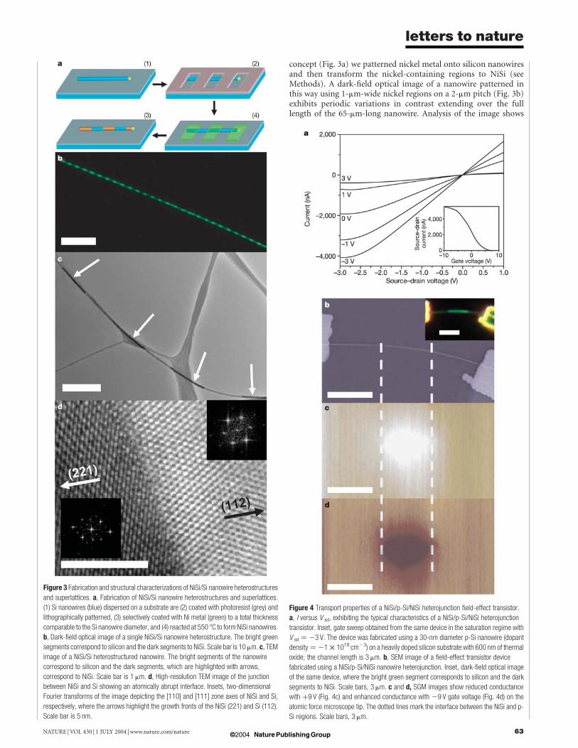
concept (Fig. 3a) we patterned nickel metal onto silicon nanowiresand then transform the nickel-containing regions to NiSi (seeMethods). A dark-field optical image of a nanowire patterned inthis way using 1-mm-wide nickel regions on a 2-mm pitch (Fig. 3b)exhibits periodic variations in contrast extending over the fulllength of the 65-mm-long nanowire. Analysis of the image shows
Figure 4 Transport properties of a NiSi/p-Si/NiSi heterojunction field-effect transistor.
a, I versus V sd, exhibiting the typical characteristics of a NiSi/p-Si/NiSi heterojunction
transistor. Inset, gate sweep obtained from the same device in the saturation regime with
V sd ¼ 23 V. The device was fabricated using a 30-nm diameter p-Si nanowire (dopant
density ¼ ,1 £ 1018 cm23) on a heavily doped silicon substrate with 600 nm of thermal
oxide; the channel length is 3mm. b, SEM image of a field-effect transistor device
fabricated using a NiSi/p-Si/NiSi nanowire heterojunction. Inset, dark-field optical image
of the same device, where the bright green segment corresponds to silicon and the dark
segments to NiSi. Scale bars, 3mm. c and d, SGM images show reduced conductance
with þ9 V (Fig. 4c) and enhanced conductance with 29 V gate voltage (Fig. 4d) on the
atomic force microscope tip. The dotted lines mark the interface between the NiSi and p-
Si regions. Scale bars, 3mm.
Figure 3 Fabrication and structural characterizations of NiSi/Si nanowire heterostructures
and superlattices. a, Fabrication of NiSi/Si nanowire heterostructures and superlattices.
(1) Si nanowires (blue) dispersed on a substrate are (2) coated with photoresist (grey) and
lithographically patterned, (3) selectively coated with Ni metal (green) to a total thickness
comparable to the Si nanowire diameter, and (4) reacted at 550 8C to form NiSi nanowires.
b, Dark-field optical image of a single NiSi/Si nanowire heterostructure. The bright green
segments correspond to silicon and the dark segments to NiSi. Scale bar is 10mm. c, TEM
image of a NiSi/Si heterostructured nanowire. The bright segments of the nanowire
correspond to silicon and the dark segments, which are highlighted with arrows,
correspond to NiSi. Scale bar is 1 mm. d, High-resolution TEM image of the junction
between NiSi and Si showing an atomically abrupt interface. Insets, two-dimensional
Fourier transforms of the image depicting the [110] and [111] zone axes of NiSi and Si,
respectively, where the arrows highlight the growth fronts of the NiSi (221) and Si (112).
Scale bar is 5 nm.
letters to nature
NATURE | VOL 430 | 1 JULY 2004 | www.nature.com/nature 63© 2004 Nature Publishing Group

that the average lengths of the Si and NiSi regions are both 1 mm, andin good agreement with the width and pitch of nickel metaldeposited on the nanowire during fabrication.
TEM images of similar NiSi/Si nanowire heterostructures(Fig. 3c) show a similar periodic variation in contrast that isconsistent with NiSi (dark) and Si (light) materials within theheterostructure. This assignment was confirmed by EDS analysis:the dark and light regions corresponded to an Ni:Si ratio of1.02:1.00 and pure Si, respectively. Analysis of the images alsoshows that the average lengths of the Si and NiSi regions are0.93 ^ 0.10 and 1.03 ^ 0.11 mm, respectively. The good agreementwith the expected pattern demonstrates clearly that our approachenables spatially controlled transformation of silicon to metallicNiSi nanowire heterostructures. Notably, detailed examination ofNiSi/Si heterostructure by high-resolution TEM (Fig. 3d) showsthat the transformation yields an atomically abrupt interface (irre-spective of any axial diffusion). The reciprocal lattice peaks, whichwere obtained from two-dimensional Fourier transforms of thelattice-resolved image (insets to Fig. 3d) correspond to the [110]and [111] zone axes of NiSi and Si, with (221) and (112) nanowiregrowth fronts, respectively.
The atomically sharp metal–semiconductor interfaces producedin these nanowire heterostructures have the potential to yield arange of precisely defined electronic devices and device arrays onindividual nanowires. To explore this opportunity we have preparedfield-effect transistor (FET) devices in which the critical source–drain regions are defined by metallic NiSi nanowire sections onp-type Si nanowire. Current versus source–drain voltage (V sd) data(Fig. 4a) are linear to jV sdj # 1 V, which suggests that the NiSi/Sicontacts behave for practical purposes as ohmic contacts at roomtemperature, although preliminary temperature-dependentmeasurements show a barrier at low temperature. The room-temperature behaviour can be explained by the reported segregationof dopant to the NiSi/Si interface during NiSi formation9, althoughother factors may also contribute to the ohmic response at roomtemperature. Notably, I–V sd data recorded at different back gate
voltages (V g) exhibit the behaviour expected17 of a depletion modep-FET with a high hole mobility of 325 cm2 V s (see Methods).
To demonstrate that the active channel of this device was definedby the separation between NiSi nanowire regions, and not the muchlarger lithographically defined metal contacts, we carried out scan-ning gate microscopy (SGM) measurements. SGM images recordedwith the scanning gate voltages of 29 V (Fig. 4c) and þ9 V (Fig. 4d)respectively show enhanced (accumulation) and reduced(depletion) conductance only in the silicon region over the overalldevice (Fig. 4b). These data thus confirm that our approach yieldsspatially and electronically well-defined metal–semiconductordevices.
Lastly, we have investigated scaling of our approach by assem-bling18 crossed-nanowire arrays in which the crossed nanowiresfunction as masks defining active channels in NiSi/Si/NiSi hetero-structures (see Methods) and could also function as local gates(Fig. 5a). TEM images recorded on a device following removal of thecrossed-nanowire mask (Fig. 5b) show a well-defined silicon chan-nel of 20 nm in this 10-nm-diameter NiSi/Si/NiSi heterostructure.This channel length is comparable to the best that can be achieved instate-of-the-art planar devices19. The TEM results indicate lateraldiffusion of several nanometres during the formation of NiSi, andsuggest that it should be possible to prepare shorter channel devicesin a well-defined manner simply by varying the diameter of thenanowire mask. More generally, the capability of transforming Si toNiSi in a spatially well-defined manner to form NiSi/Si nanowireheterostructures and superlattices with atomically sharp metal–semiconductor interfaces opens up the possibility of integratingboth active devices and high-performance interconnects from asingle nanoscale building block. By extending our approach tocrossed nanowires as shown above it should become possible toassemble large and dense arrays, perhaps using Langmuir–Blodgettassembly techniques20, of transistors and other devices that couldenable hybrid integrated circuits and could represent a key steptowards stand-alone integrated nanosystems. A
MethodsPreparation of single-crystal metallic NiSi nanowiresSi nanowires were synthesized via chemical vapour deposition using monodisperse goldnanoclusters (Ted Pella) as catalysts, silane (SiH4) as the vapour-phase reactant, diboraneas the dopant and hydrogen as the carrier gas10,11. The silicon nanowires produced in thismanner have clean surfaces with no visible amorphous oxide11. Immediately followingsynthesis, the growth substrate with uniform diameter, free-standing Si nanowires wasloaded into a metal deposition system, and then Ni metal was deposited to a thicknesscomparable to the average Si nanowire diameter. NiSi nanowires were produced byannealing the Ni-metal-coated Si nanowires at 550 8C. Excess Ni was completely removedby etching (TFG, Transene) for one hour at 50 8C, followed by post-annealing at 600 8C.Each of the annealing steps was carried out in forming gas (N2:H2 ratio, 90:10) for 5 min ina rapid thermal annealer (Heatpulse 610, Metron Technology).
Preparation of NiSi/Si nanowire heterostructuresSi nanowires dispersed in ethanol were deposited on a Si wafer with 600 nm of thermaloxide, and then the substrate was coated with photoresist (Shipley 1813, Rohm and HaasElectronics Materials). The photoresist was exposed for about 2 s on an ABM photoalignerusing a simple striped pattern with a 2-mm pitch: 1mm linewidth and 1 mm spacing. Afterdeveloping for 1 min, the wafer was transferred to a thermal evaporator and Ni wasevaporated with a thickness equal to the average nanowire diameter. After lift-off, thesamples were annealed and etched as described above. Ultrasmall NiSi/Si/NiSi nanowireheterostructures were fabricated using crossed Si/SiO2 core-shell nanowires21 as masks todefine the lengths of the unreacted Si regions. The crossed-nanowire structures wereassembled on Si3N4 membrane window grids (Structure Probe) by fluidic assembly18, andthen Ni was evaporated and annealed as described above. The Si/SiO2 core–shellnanowires were removed with hydrogen fluoride solution (Transene) to enable directTEM imaging of the NiSi/Si/NiSi heterostructure on the Si3N4 membranes.
Calculation of device characteristicsThe hole mobility, m, is computed using a standard model17. In the small bias lineartransport region, the mobility is expressed in terms of the transconductance, g m, asg m ¼ mCV sd/L2, where V sd is the source–drain voltage, L is the device channel length, andC is the gate capacitance, which was estimated using C ¼ 2pee 0L/ln(2t ox/r) (where e is theeffective dielectric constant, tox is the SiO2 dielectric thickness, and r is the nanowireradius). For the device in Fig. 3a, gm was evaluated for Vg from 23 to þ 3 Vat V sd ¼ –1 V,and has a value of 275 nS.
Figure 5 Self-aligned nanoscale NiSi/Si/NiSi devices. a, Schematic illustrating Si
nanowire (blue) crossed with three Si/SiO2 core (blue)–shell (grey) nanowires21.
Deposition, annealing and removal of excess Ni yields NiSi (brown) regions separated by Si
in the nanowire. b, TEM image of the NiSi/Si/NiSi nanowire heterostructure. The dark
regions correspond to NiSi and the light region to Si with NiSi/Si interfaces highlighted by
black arrows. Scale bar is 10 nm. Inset, TEM image of the same nanowire before
silicidation. The crossed Si/SiO2 core–shell nanowire (approximately vertical in image)
was used as a mask to define the Si region and removed after silicidation. Scale bar is
20 nm. The sample was prepared and imaged on a 50-nm-thick Si3N4 membrane.
letters to nature
NATURE | VOL 430 | 1 JULY 2004 | www.nature.com/nature64 © 2004 Nature Publishing Group

Received 1 March; accepted 24 May 2004; doi:10.1038/nature02674.
1. Yao, Z., Dekker, C. & Avouris, Ph. Electrical transport through single-wall carbon nanotubes. Top.
Appl. Phys. 80, 147–171 (2001).
2. McEuen, P. L., Fuhrer, M. S. & Park, H. Single-walled carbon nanotube electronics. IEEE Trans.
Nanotechnol. 1, 78–85 (2002).
3. Dai, H. Carbon nanotubes: synthesis, integration, and properties. Acc. Chem. Res. 35, 1035–1044
(2002).
4. Lieber, C. M. Nanoscale science and technology: Building a big future from small things. MRS Bull. 28,
486–491 (2003).
5. Lieber, C. M. The incredible shrinking circuit. Sci. Am. 285, 58–64 (2001).
6. Cui, Y., Zhong, Z., Wang, D., Wang, W. U. & Lieber, C. M. High performance silicon nanowire field
effect transistors. Nano Lett. 3, 149–152 (2003).
7. Javey, A., Guo, J., Wang, Q., Lundstrom, M. & Dai, H. Ballistic carbon nanotube field-effect
transistors. Nature 424, 654–657 (2003).
8. Heinze, S. et al. Carbon nanotubes as Schottky barrier transistors. Phys. Rev. Lett. 89, 106801 (2002).
9. Morimoto, T. et al. Self-aligned nickel-mono-silicide technology for high-speed deep submicrometer
logic CMOS ULSI. IEEE Trans. Electron Devices 42, 915–922 (1995).
10. Cui, Y., Lauhon, L. J., Gudiksen, M. S., Wang, J. & Lieber, C. M. Diameter-controlled synthesis of
single-crystal silicon nanowires. Appl. Phys. Lett. 78, 2214–2216 (2001).
11. Wu, Y. et al. Controlled growth and structures of molecular-scale silicon nanowires. Nano Lett. 4,
433–436 (2004).
12. Toman, K. The structure of NiSi. Acta Crystallogr. 4, 462–464 (1951).
13. Meyer, B. et al. Intrinsic properties of NiSi. J. Alloys Compounds 262/263, 235–237 (1997).
14. Pierce, D. G. & Brusius, P. G. Electromigration: a review. Microelectron. Reliab. 37, 1053–1072 (1997).
15. Yao, Z., Kane, C. L. & Dekker, C. High-field electrical transport in single-wall carbon nanotubes. Phys.
Rev. Lett. 84, 2941–2944 (2000).
16. International Technology Roadmap for Semiconductors 2003 edn khttp://public.itrs.net/Files/
2003ITRS/Interconnect2003.pdfl (2003).
17. Sze, S. M. Physics of Semicondutor Devices 438–445 (John Wiley & Sons, New York, 1981).
18. Huang, Y., Duan, X., Wei, Q. & Lieber, C. M. Directed assembly of one-dimensional nanostructures
into functional networks. Science 291, 630–633 (2001).
19. Chau, R. et al. Silicon nano-transistors for logic applications. Physica E 19, 1–5 (2003).
20. Whang, D., Jin, S., Wu, Y. & Lieber, C. M. Large-scale hierarchical organization of nanowire arrays for
integrated nanosystems. Nano Lett. 3, 1255–1259 (2003).
21. Lauhon, L. J., Gudiksen, M. S., Wang, D. & Lieber, C. M. Epitaxial core–shell and core–multishell
nanowire heterostructures. Nature 420, 57–61 (2002).
Acknowledgements We thank M. C. McAlpine, C. J. Barrelet and D. C. Bell for discussions.
C.M.L. thanks the Defense Advanced Research Projects Agency and Intel for support of this work.
Competing interests statement The authors declare that they have no competing financial
interests.
Correspondence and requests for materials should be addressed to C.M.L.
..............................................................
Evidence for deep-water productionin the North Pacific Ocean duringthe early Cenozoic warm intervalDeborah J. Thomas
Department of Oceanography, Texas A&M University, College Station,Texas 77843-3146, USA.............................................................................................................................................................................
The deep-ocean circulation is responsible for a significant com-ponent of global heat transport. In the present mode of circula-tion, deep waters form in the North Atlantic and Southern oceanswhere surface water becomes sufficiently cold and dense to sink.Polar temperatures during the warmest climatic interval of theCenozoic era (,65 to 40 million years (Myr) ago) were signifi-cantly warmer than today, and this may have been a consequenceof enhanced oceanic heat transport1. However, understanding therelationship between deep-ocean circulation and ancient climateis complicated by differences in oceanic gateways2, which affectwhere deep waters form and how they circulate. Here I reportrecords of neodymium isotopes from two cores in the PacificOcean that indicate a shift in deep-water production from theSouthern Ocean to the North Pacific,65 Myr ago. The source ofdeep waters reverted back to the SouthernOcean 40Myr ago. The
relative timing of changes in the neodymium and oxygen isotoperecords indicates that changes in Cenozoic deep-water circula-tion patterns were the consequence, not the cause, of extremeCenozoic warmth.
Slow deep-water renewal in the modern North Pacific is aconsequence of climatic and tectonic factors. Relatively high pre-cipitation in the North Pacific3 results in sea-surface salinities toolow to enable downwelling (,33 parts per thousand (p.p.t.) ascompared to ,35 p.p.t. in the North Atlantic3). Further, the BeringStrait sill does not permit dense, cold Arctic bottom waters to enterthe North Pacific4. In addition, most of the bottom waters formed inthe Ross Sea (the Pacific sector of the Southern Ocean) areprevented from flowing northward into the Pacific basin by theeastward flow of the Antarctic circumpolar current and the mid-ocean ridge4.
However, a different set of climatic and tectonic boundaryconditions prevailed during the early Cenozoic interval of extremewarmth, about 65–40 Myr ago. Global deep-water temperatureswere about 8–12 8C (ref. 5), too warm for permanent polar ice toexist. The configuration of continents and ocean basins was alsodifferent from the present (Fig. 1). The Tasman Sea and DrakePassage had not yet opened, and Tethyan and Caribbean seawaysstill existed2. In addition, the Norwegian and Greenland seas beganforming ,55 Myr ago6, so North Atlantic deep waters would nothave existed during this time interval.
Such different thermal and palaeogeographic regimes shouldhave affected deep-sea circulation patterns, and conversely, adifferent mode of thermohaline circulation may have influencedthe evolution of global climate. To investigate the relationshipbetween early Cenozoic climate and thermohaline circulationpatterns, I generated records of the neodymium isotopic compo-sition of fossil fish debris from Ocean Drilling Program (ODP) Sites1209 and 1211 (Shatsky rise, in the present-day northwesternPacific).
Neodymium isotopic ratios (143Nd/144Nd, expressed as e Nd;ref. 7) track deep-water mass circulation because Nd has a shortoceanic residence time (,1,000 yr; ref. 8) relative to oceanic mixing(,1,500 yr; ref. 9). The e Nd composition of individual deep-watermasses is derived from the composition of Nd discharging intothe source regions of the water masses10–12. South Pacific surface
Figure 1 Palaeogeographic reconstructions during two intervals of the early Cenozoic.
The location of Ocean Drilling Program (ODP) Sites 1209 and 1211 are shown for 65 Myr
ago (top panels) and 40 Myr ago (bottom panels). Note that the location of Sites 1209 and
1211 did not change significantly over the time interval investigated. Reconstructions
created by the Ocean Drilling Stratigraphic Network (www.odsn.de).
letters to nature
NATURE | VOL 430 | 1 JULY 2004 | www.nature.com/nature 65© 2004 Nature Publishing Group